KR20120090779A - Method for manufacturing semiconductor device - Google Patents
Method for manufacturing semiconductor device Download PDFInfo
- Publication number
- KR20120090779A KR20120090779A KR1020120003336A KR20120003336A KR20120090779A KR 20120090779 A KR20120090779 A KR 20120090779A KR 1020120003336 A KR1020120003336 A KR 1020120003336A KR 20120003336 A KR20120003336 A KR 20120003336A KR 20120090779 A KR20120090779 A KR 20120090779A
- Authority
- KR
- South Korea
- Prior art keywords
- transistor
- electrode
- film
- oxide semiconductor
- semiconductor film
- Prior art date
Links
- 239000004065 semiconductor Substances 0.000 title claims abstract description 317
- 238000000034 method Methods 0.000 title claims abstract description 57
- 238000004519 manufacturing process Methods 0.000 title claims abstract description 14
- 239000000758 substrate Substances 0.000 claims abstract description 126
- 239000013078 crystal Substances 0.000 claims description 37
- 238000010438 heat treatment Methods 0.000 claims description 32
- 238000009413 insulation Methods 0.000 abstract 4
- 239000010408 film Substances 0.000 description 295
- 239000004973 liquid crystal related substance Substances 0.000 description 75
- QVGXLLKOCUKJST-UHFFFAOYSA-N atomic oxygen Chemical compound [O] QVGXLLKOCUKJST-UHFFFAOYSA-N 0.000 description 57
- 229910052760 oxygen Inorganic materials 0.000 description 57
- 239000001301 oxygen Substances 0.000 description 57
- 239000010410 layer Substances 0.000 description 44
- 239000000463 material Substances 0.000 description 41
- 239000003990 capacitor Substances 0.000 description 37
- 230000015572 biosynthetic process Effects 0.000 description 28
- 125000004429 atom Chemical group 0.000 description 24
- IJGRMHOSHXDMSA-UHFFFAOYSA-N Atomic nitrogen Chemical compound N#N IJGRMHOSHXDMSA-UHFFFAOYSA-N 0.000 description 21
- VUFNLQXQSDUXKB-DOFZRALJSA-N 2-[4-[4-[bis(2-chloroethyl)amino]phenyl]butanoyloxy]ethyl (5z,8z,11z,14z)-icosa-5,8,11,14-tetraenoate Chemical compound CCCCC\C=C/C\C=C/C\C=C/C\C=C/CCCC(=O)OCCOC(=O)CCCC1=CC=C(N(CCCl)CCCl)C=C1 VUFNLQXQSDUXKB-DOFZRALJSA-N 0.000 description 19
- 239000002585 base Substances 0.000 description 19
- 238000010586 diagram Methods 0.000 description 19
- XLOMVQKBTHCTTD-UHFFFAOYSA-N Zinc monoxide Chemical compound [Zn]=O XLOMVQKBTHCTTD-UHFFFAOYSA-N 0.000 description 16
- 229910007541 Zn O Inorganic materials 0.000 description 16
- 125000004430 oxygen atom Chemical group O* 0.000 description 14
- XUIMIQQOPSSXEZ-UHFFFAOYSA-N Silicon Chemical compound [Si] XUIMIQQOPSSXEZ-UHFFFAOYSA-N 0.000 description 13
- 238000005401 electroluminescence Methods 0.000 description 13
- 230000006870 function Effects 0.000 description 13
- 239000007789 gas Substances 0.000 description 13
- 239000011701 zinc Substances 0.000 description 13
- 206010021143 Hypoxia Diseases 0.000 description 12
- 238000010521 absorption reaction Methods 0.000 description 12
- 150000002500 ions Chemical class 0.000 description 12
- 229910052751 metal Inorganic materials 0.000 description 12
- 229910052710 silicon Inorganic materials 0.000 description 12
- 238000004364 calculation method Methods 0.000 description 11
- 230000005684 electric field Effects 0.000 description 11
- 239000002184 metal Substances 0.000 description 11
- 229910052757 nitrogen Inorganic materials 0.000 description 11
- 239000010703 silicon Substances 0.000 description 11
- 238000003860 storage Methods 0.000 description 10
- 229910052733 gallium Inorganic materials 0.000 description 9
- 230000001590 oxidative effect Effects 0.000 description 9
- 238000004458 analytical method Methods 0.000 description 8
- 239000001257 hydrogen Substances 0.000 description 8
- 229910052739 hydrogen Inorganic materials 0.000 description 8
- 239000012535 impurity Substances 0.000 description 8
- 239000011229 interlayer Substances 0.000 description 8
- 239000011787 zinc oxide Substances 0.000 description 8
- 241001270131 Agaricus moelleri Species 0.000 description 7
- 239000011521 glass Substances 0.000 description 7
- 229910052738 indium Inorganic materials 0.000 description 7
- 229910052725 zinc Inorganic materials 0.000 description 7
- 229910052782 aluminium Inorganic materials 0.000 description 6
- 230000008859 change Effects 0.000 description 6
- 239000000203 mixture Substances 0.000 description 6
- 230000008569 process Effects 0.000 description 6
- UFHFLCQGNIYNRP-UHFFFAOYSA-N Hydrogen Chemical compound [H][H] UFHFLCQGNIYNRP-UHFFFAOYSA-N 0.000 description 5
- 230000005669 field effect Effects 0.000 description 5
- 239000011159 matrix material Substances 0.000 description 5
- 230000003071 parasitic effect Effects 0.000 description 5
- VYPSYNLAJGMNEJ-UHFFFAOYSA-N silicon dioxide Inorganic materials O=[Si]=O VYPSYNLAJGMNEJ-UHFFFAOYSA-N 0.000 description 5
- GQPLMRYTRLFLPF-UHFFFAOYSA-N Nitrous Oxide Chemical compound [O-][N+]#N GQPLMRYTRLFLPF-UHFFFAOYSA-N 0.000 description 4
- HCHKCACWOHOZIP-UHFFFAOYSA-N Zinc Chemical compound [Zn] HCHKCACWOHOZIP-UHFFFAOYSA-N 0.000 description 4
- 239000000969 carrier Substances 0.000 description 4
- 229920001940 conductive polymer Polymers 0.000 description 4
- 230000012010 growth Effects 0.000 description 4
- APFVFJFRJDLVQX-UHFFFAOYSA-N indium atom Chemical compound [In] APFVFJFRJDLVQX-UHFFFAOYSA-N 0.000 description 4
- 230000002093 peripheral effect Effects 0.000 description 4
- 229910052814 silicon oxide Inorganic materials 0.000 description 4
- 125000006850 spacer group Chemical group 0.000 description 4
- 101001047514 Bos taurus Lethal(2) giant larvae protein homolog 1 Proteins 0.000 description 3
- MYMOFIZGZYHOMD-UHFFFAOYSA-N Dioxygen Chemical compound O=O MYMOFIZGZYHOMD-UHFFFAOYSA-N 0.000 description 3
- 244000126211 Hericium coralloides Species 0.000 description 3
- 229910019092 Mg-O Inorganic materials 0.000 description 3
- 229910019395 Mg—O Inorganic materials 0.000 description 3
- 229910052581 Si3N4 Inorganic materials 0.000 description 3
- 229910052783 alkali metal Inorganic materials 0.000 description 3
- 150000001340 alkali metals Chemical class 0.000 description 3
- 238000004380 ashing Methods 0.000 description 3
- 230000015556 catabolic process Effects 0.000 description 3
- 229910052801 chlorine Inorganic materials 0.000 description 3
- 230000000694 effects Effects 0.000 description 3
- 238000005530 etching Methods 0.000 description 3
- 239000005262 ferroelectric liquid crystals (FLCs) Substances 0.000 description 3
- 229910052731 fluorine Inorganic materials 0.000 description 3
- 150000002431 hydrogen Chemical class 0.000 description 3
- 230000014759 maintenance of location Effects 0.000 description 3
- 230000007246 mechanism Effects 0.000 description 3
- 229910044991 metal oxide Inorganic materials 0.000 description 3
- 150000004706 metal oxides Chemical group 0.000 description 3
- 229910021421 monocrystalline silicon Inorganic materials 0.000 description 3
- 230000003287 optical effect Effects 0.000 description 3
- 238000005457 optimization Methods 0.000 description 3
- 150000002894 organic compounds Chemical class 0.000 description 3
- 229920002620 polyvinyl fluoride Polymers 0.000 description 3
- 239000003566 sealing material Substances 0.000 description 3
- HQVNEWCFYHHQES-UHFFFAOYSA-N silicon nitride Chemical compound N12[Si]34N5[Si]62N3[Si]51N64 HQVNEWCFYHHQES-UHFFFAOYSA-N 0.000 description 3
- 230000003068 static effect Effects 0.000 description 3
- 239000010409 thin film Substances 0.000 description 3
- 229910052719 titanium Inorganic materials 0.000 description 3
- 239000010936 titanium Substances 0.000 description 3
- PAYRUJLWNCNPSJ-UHFFFAOYSA-N Aniline Chemical compound NC1=CC=CC=C1 PAYRUJLWNCNPSJ-UHFFFAOYSA-N 0.000 description 2
- XKRFYHLGVUSROY-UHFFFAOYSA-N Argon Chemical compound [Ar] XKRFYHLGVUSROY-UHFFFAOYSA-N 0.000 description 2
- 102100040844 Dual specificity protein kinase CLK2 Human genes 0.000 description 2
- GYHNNYVSQQEPJS-UHFFFAOYSA-N Gallium Chemical compound [Ga] GYHNNYVSQQEPJS-UHFFFAOYSA-N 0.000 description 2
- 101000749291 Homo sapiens Dual specificity protein kinase CLK2 Proteins 0.000 description 2
- CBENFWSGALASAD-UHFFFAOYSA-N Ozone Chemical compound [O-][O+]=O CBENFWSGALASAD-UHFFFAOYSA-N 0.000 description 2
- OAICVXFJPJFONN-UHFFFAOYSA-N Phosphorus Chemical compound [P] OAICVXFJPJFONN-UHFFFAOYSA-N 0.000 description 2
- KAESVJOAVNADME-UHFFFAOYSA-N Pyrrole Chemical compound C=1C=CNC=1 KAESVJOAVNADME-UHFFFAOYSA-N 0.000 description 2
- YTPLMLYBLZKORZ-UHFFFAOYSA-N Thiophene Chemical compound C=1C=CSC=1 YTPLMLYBLZKORZ-UHFFFAOYSA-N 0.000 description 2
- GWEVSGVZZGPLCZ-UHFFFAOYSA-N Titan oxide Chemical compound O=[Ti]=O GWEVSGVZZGPLCZ-UHFFFAOYSA-N 0.000 description 2
- 229910052784 alkaline earth metal Inorganic materials 0.000 description 2
- 150000001342 alkaline earth metals Chemical class 0.000 description 2
- XAGFODPZIPBFFR-UHFFFAOYSA-N aluminium Chemical compound [Al] XAGFODPZIPBFFR-UHFFFAOYSA-N 0.000 description 2
- 229910021417 amorphous silicon Inorganic materials 0.000 description 2
- 229910052785 arsenic Inorganic materials 0.000 description 2
- RQNWIZPPADIBDY-UHFFFAOYSA-N arsenic atom Chemical compound [As] RQNWIZPPADIBDY-UHFFFAOYSA-N 0.000 description 2
- 239000000460 chlorine Substances 0.000 description 2
- 239000003086 colorant Substances 0.000 description 2
- 150000001875 compounds Chemical class 0.000 description 2
- 239000004020 conductor Substances 0.000 description 2
- 229910052802 copper Inorganic materials 0.000 description 2
- 239000010949 copper Substances 0.000 description 2
- 238000002425 crystallisation Methods 0.000 description 2
- 230000008025 crystallization Effects 0.000 description 2
- 238000003795 desorption Methods 0.000 description 2
- 230000006866 deterioration Effects 0.000 description 2
- 238000001312 dry etching Methods 0.000 description 2
- 230000005611 electricity Effects 0.000 description 2
- 239000000284 extract Substances 0.000 description 2
- 239000011152 fibreglass Substances 0.000 description 2
- 239000011737 fluorine Substances 0.000 description 2
- 229910052732 germanium Inorganic materials 0.000 description 2
- 125000005842 heteroatom Chemical group 0.000 description 2
- 229910003437 indium oxide Inorganic materials 0.000 description 2
- PJXISJQVUVHSOJ-UHFFFAOYSA-N indium(iii) oxide Chemical compound [O-2].[O-2].[O-2].[In+3].[In+3] PJXISJQVUVHSOJ-UHFFFAOYSA-N 0.000 description 2
- AMGQUBHHOARCQH-UHFFFAOYSA-N indium;oxotin Chemical compound [In].[Sn]=O AMGQUBHHOARCQH-UHFFFAOYSA-N 0.000 description 2
- 239000011261 inert gas Substances 0.000 description 2
- 238000002347 injection Methods 0.000 description 2
- 239000007924 injection Substances 0.000 description 2
- 239000012212 insulator Substances 0.000 description 2
- 238000005468 ion implantation Methods 0.000 description 2
- 238000003475 lamination Methods 0.000 description 2
- 229910052748 manganese Inorganic materials 0.000 description 2
- 238000002156 mixing Methods 0.000 description 2
- 229910052759 nickel Inorganic materials 0.000 description 2
- 239000001272 nitrous oxide Substances 0.000 description 2
- QGLKJKCYBOYXKC-UHFFFAOYSA-N nonaoxidotritungsten Chemical compound O=[W]1(=O)O[W](=O)(=O)O[W](=O)(=O)O1 QGLKJKCYBOYXKC-UHFFFAOYSA-N 0.000 description 2
- 239000011574 phosphorus Substances 0.000 description 2
- 229910052698 phosphorus Inorganic materials 0.000 description 2
- 239000004033 plastic Substances 0.000 description 2
- 229920003023 plastic Polymers 0.000 description 2
- 229920006267 polyester film Polymers 0.000 description 2
- 230000009467 reduction Effects 0.000 description 2
- HBMJWWWQQXIZIP-UHFFFAOYSA-N silicon carbide Chemical compound [Si+]#[C-] HBMJWWWQQXIZIP-UHFFFAOYSA-N 0.000 description 2
- 229910010271 silicon carbide Inorganic materials 0.000 description 2
- LIVNPJMFVYWSIS-UHFFFAOYSA-N silicon monoxide Chemical compound [Si-]#[O+] LIVNPJMFVYWSIS-UHFFFAOYSA-N 0.000 description 2
- 238000004544 sputter deposition Methods 0.000 description 2
- 239000000126 substance Substances 0.000 description 2
- 229910052718 tin Inorganic materials 0.000 description 2
- 239000011135 tin Substances 0.000 description 2
- OGIDPMRJRNCKJF-UHFFFAOYSA-N titanium oxide Inorganic materials [Ti]=O OGIDPMRJRNCKJF-UHFFFAOYSA-N 0.000 description 2
- 229910052721 tungsten Inorganic materials 0.000 description 2
- 229910001930 tungsten oxide Inorganic materials 0.000 description 2
- YVTHLONGBIQYBO-UHFFFAOYSA-N zinc indium(3+) oxygen(2-) Chemical compound [O--].[Zn++].[In+3] YVTHLONGBIQYBO-UHFFFAOYSA-N 0.000 description 2
- 239000004925 Acrylic resin Substances 0.000 description 1
- 229920000178 Acrylic resin Polymers 0.000 description 1
- JBRZTFJDHDCESZ-UHFFFAOYSA-N AsGa Chemical compound [As]#[Ga] JBRZTFJDHDCESZ-UHFFFAOYSA-N 0.000 description 1
- 102100040862 Dual specificity protein kinase CLK1 Human genes 0.000 description 1
- 229910002601 GaN Inorganic materials 0.000 description 1
- 229910001218 Gallium arsenide Inorganic materials 0.000 description 1
- JMASRVWKEDWRBT-UHFFFAOYSA-N Gallium nitride Chemical compound [Ga]#N JMASRVWKEDWRBT-UHFFFAOYSA-N 0.000 description 1
- 239000005264 High molar mass liquid crystal Substances 0.000 description 1
- 101000749294 Homo sapiens Dual specificity protein kinase CLK1 Proteins 0.000 description 1
- 241001591005 Siga Species 0.000 description 1
- 229910000577 Silicon-germanium Inorganic materials 0.000 description 1
- 239000004990 Smectic liquid crystal Substances 0.000 description 1
- 229910020923 Sn-O Inorganic materials 0.000 description 1
- 239000004974 Thermotropic liquid crystal Substances 0.000 description 1
- ATJFFYVFTNAWJD-UHFFFAOYSA-N Tin Chemical compound [Sn] ATJFFYVFTNAWJD-UHFFFAOYSA-N 0.000 description 1
- RTAQQCXQSZGOHL-UHFFFAOYSA-N Titanium Chemical compound [Ti] RTAQQCXQSZGOHL-UHFFFAOYSA-N 0.000 description 1
- LEVVHYCKPQWKOP-UHFFFAOYSA-N [Si].[Ge] Chemical compound [Si].[Ge] LEVVHYCKPQWKOP-UHFFFAOYSA-N 0.000 description 1
- 230000009471 action Effects 0.000 description 1
- 230000002411 adverse Effects 0.000 description 1
- 229910045601 alloy Inorganic materials 0.000 description 1
- 239000000956 alloy Substances 0.000 description 1
- 229910052786 argon Inorganic materials 0.000 description 1
- 238000000231 atomic layer deposition Methods 0.000 description 1
- 239000011230 binding agent Substances 0.000 description 1
- 239000000919 ceramic Substances 0.000 description 1
- 238000005229 chemical vapour deposition Methods 0.000 description 1
- 125000001309 chloro group Chemical group Cl* 0.000 description 1
- 230000003098 cholesteric effect Effects 0.000 description 1
- 229910052804 chromium Inorganic materials 0.000 description 1
- 229920001577 copolymer Polymers 0.000 description 1
- 230000006378 damage Effects 0.000 description 1
- 230000007547 defect Effects 0.000 description 1
- 230000007812 deficiency Effects 0.000 description 1
- 238000006731 degradation reaction Methods 0.000 description 1
- 238000009792 diffusion process Methods 0.000 description 1
- 239000006185 dispersion Substances 0.000 description 1
- 239000004815 dispersion polymer Substances 0.000 description 1
- 125000001153 fluoro group Chemical group F* 0.000 description 1
- 239000011888 foil Substances 0.000 description 1
- GNPVGFCGXDBREM-UHFFFAOYSA-N germanium atom Chemical compound [Ge] GNPVGFCGXDBREM-UHFFFAOYSA-N 0.000 description 1
- 229910000449 hafnium oxide Inorganic materials 0.000 description 1
- WIHZLLGSGQNAGK-UHFFFAOYSA-N hafnium(4+);oxygen(2-) Chemical compound [O-2].[O-2].[Hf+4] WIHZLLGSGQNAGK-UHFFFAOYSA-N 0.000 description 1
- 239000001307 helium Substances 0.000 description 1
- 229910052734 helium Inorganic materials 0.000 description 1
- SWQJXJOGLNCZEY-UHFFFAOYSA-N helium atom Chemical compound [He] SWQJXJOGLNCZEY-UHFFFAOYSA-N 0.000 description 1
- 125000004435 hydrogen atom Chemical group [H]* 0.000 description 1
- 238000005286 illumination Methods 0.000 description 1
- 150000002484 inorganic compounds Chemical class 0.000 description 1
- 229910010272 inorganic material Inorganic materials 0.000 description 1
- 229910052743 krypton Inorganic materials 0.000 description 1
- DNNSSWSSYDEUBZ-UHFFFAOYSA-N krypton atom Chemical compound [Kr] DNNSSWSSYDEUBZ-UHFFFAOYSA-N 0.000 description 1
- 238000010030 laminating Methods 0.000 description 1
- 230000007257 malfunction Effects 0.000 description 1
- 229910021645 metal ion Inorganic materials 0.000 description 1
- 238000001451 molecular beam epitaxy Methods 0.000 description 1
- 229910052750 molybdenum Inorganic materials 0.000 description 1
- 229910052754 neon Inorganic materials 0.000 description 1
- GKAOGPIIYCISHV-UHFFFAOYSA-N neon atom Chemical compound [Ne] GKAOGPIIYCISHV-UHFFFAOYSA-N 0.000 description 1
- PXHVJJICTQNCMI-UHFFFAOYSA-N nickel Substances [Ni] PXHVJJICTQNCMI-UHFFFAOYSA-N 0.000 description 1
- 150000004767 nitrides Chemical class 0.000 description 1
- QJGQUHMNIGDVPM-UHFFFAOYSA-N nitrogen group Chemical group [N] QJGQUHMNIGDVPM-UHFFFAOYSA-N 0.000 description 1
- 230000003647 oxidation Effects 0.000 description 1
- 238000007254 oxidation reaction Methods 0.000 description 1
- TWNQGVIAIRXVLR-UHFFFAOYSA-N oxo(oxoalumanyloxy)alumane Chemical compound O=[Al]O[Al]=O TWNQGVIAIRXVLR-UHFFFAOYSA-N 0.000 description 1
- SIWVEOZUMHYXCS-UHFFFAOYSA-N oxo(oxoyttriooxy)yttrium Chemical compound O=[Y]O[Y]=O SIWVEOZUMHYXCS-UHFFFAOYSA-N 0.000 description 1
- DOVLZBWRSUUIJA-UHFFFAOYSA-N oxotin;silicon Chemical compound [Si].[Sn]=O DOVLZBWRSUUIJA-UHFFFAOYSA-N 0.000 description 1
- RVTZCBVAJQQJTK-UHFFFAOYSA-N oxygen(2-);zirconium(4+) Chemical compound [O-2].[O-2].[Zr+4] RVTZCBVAJQQJTK-UHFFFAOYSA-N 0.000 description 1
- 239000002245 particle Substances 0.000 description 1
- 230000000737 periodic effect Effects 0.000 description 1
- 238000009832 plasma treatment Methods 0.000 description 1
- 230000010287 polarization Effects 0.000 description 1
- 229920000767 polyaniline Polymers 0.000 description 1
- 229910021420 polycrystalline silicon Inorganic materials 0.000 description 1
- 229920000128 polypyrrole Polymers 0.000 description 1
- 229920000123 polythiophene Polymers 0.000 description 1
- 230000000750 progressive effect Effects 0.000 description 1
- 238000004698 pseudo-potential method Methods 0.000 description 1
- 238000004549 pulsed laser deposition Methods 0.000 description 1
- 239000010453 quartz Substances 0.000 description 1
- 230000006798 recombination Effects 0.000 description 1
- 238000005215 recombination Methods 0.000 description 1
- 230000000717 retained effect Effects 0.000 description 1
- 238000005001 rutherford backscattering spectroscopy Methods 0.000 description 1
- 229910052594 sapphire Inorganic materials 0.000 description 1
- 239000010980 sapphire Substances 0.000 description 1
- 238000007789 sealing Methods 0.000 description 1
- 238000001004 secondary ion mass spectrometry Methods 0.000 description 1
- 229910052709 silver Inorganic materials 0.000 description 1
- 239000002356 single layer Substances 0.000 description 1
- 239000000243 solution Substances 0.000 description 1
- 238000004611 spectroscopical analysis Methods 0.000 description 1
- 229910052715 tantalum Inorganic materials 0.000 description 1
- JBQYATWDVHIOAR-UHFFFAOYSA-N tellanylidenegermanium Chemical compound [Te]=[Ge] JBQYATWDVHIOAR-UHFFFAOYSA-N 0.000 description 1
- 229930192474 thiophene Natural products 0.000 description 1
- 230000007704 transition Effects 0.000 description 1
- XLYOFNOQVPJJNP-UHFFFAOYSA-N water Substances O XLYOFNOQVPJJNP-UHFFFAOYSA-N 0.000 description 1
- 229910052724 xenon Inorganic materials 0.000 description 1
- FHNFHKCVQCLJFQ-UHFFFAOYSA-N xenon atom Chemical compound [Xe] FHNFHKCVQCLJFQ-UHFFFAOYSA-N 0.000 description 1
- 229910052727 yttrium Inorganic materials 0.000 description 1
- 229910001656 zinc mineral Inorganic materials 0.000 description 1
- 229910052726 zirconium Inorganic materials 0.000 description 1
- 229910001928 zirconium oxide Inorganic materials 0.000 description 1
Images


Classifications
-
- H—ELECTRICITY
- H01—ELECTRIC ELEMENTS
- H01L—SEMICONDUCTOR DEVICES NOT COVERED BY CLASS H10
- H01L29/00—Semiconductor devices adapted for rectifying, amplifying, oscillating or switching, or capacitors or resistors with at least one potential-jump barrier or surface barrier, e.g. PN junction depletion layer or carrier concentration layer; Details of semiconductor bodies or of electrodes thereof ; Multistep manufacturing processes therefor
- H01L29/66—Types of semiconductor device ; Multistep manufacturing processes therefor
- H01L29/68—Types of semiconductor device ; Multistep manufacturing processes therefor controllable by only the electric current supplied, or only the electric potential applied, to an electrode which does not carry the current to be rectified, amplified or switched
- H01L29/76—Unipolar devices, e.g. field effect transistors
- H01L29/772—Field effect transistors
- H01L29/78—Field effect transistors with field effect produced by an insulated gate
- H01L29/786—Thin film transistors, i.e. transistors with a channel being at least partly a thin film
- H01L29/7869—Thin film transistors, i.e. transistors with a channel being at least partly a thin film having a semiconductor body comprising an oxide semiconductor material, e.g. zinc oxide, copper aluminium oxide, cadmium stannate
-
- H—ELECTRICITY
- H01—ELECTRIC ELEMENTS
- H01L—SEMICONDUCTOR DEVICES NOT COVERED BY CLASS H10
- H01L29/00—Semiconductor devices adapted for rectifying, amplifying, oscillating or switching, or capacitors or resistors with at least one potential-jump barrier or surface barrier, e.g. PN junction depletion layer or carrier concentration layer; Details of semiconductor bodies or of electrodes thereof ; Multistep manufacturing processes therefor
- H01L29/40—Electrodes ; Multistep manufacturing processes therefor
- H01L29/41—Electrodes ; Multistep manufacturing processes therefor characterised by their shape, relative sizes or dispositions
- H01L29/417—Electrodes ; Multistep manufacturing processes therefor characterised by their shape, relative sizes or dispositions carrying the current to be rectified, amplified or switched
- H01L29/41725—Source or drain electrodes for field effect devices
- H01L29/41733—Source or drain electrodes for field effect devices for thin film transistors with insulated gate
Landscapes
- Microelectronics & Electronic Packaging (AREA)
- Engineering & Computer Science (AREA)
- Power Engineering (AREA)
- Condensed Matter Physics & Semiconductors (AREA)
- General Physics & Mathematics (AREA)
- Physics & Mathematics (AREA)
- Ceramic Engineering (AREA)
- Computer Hardware Design (AREA)
- Thin Film Transistor (AREA)
- Liquid Crystal (AREA)
- Semiconductor Memories (AREA)
- Devices For Indicating Variable Information By Combining Individual Elements (AREA)
- Electroluminescent Light Sources (AREA)
- Non-Volatile Memory (AREA)
- Recrystallisation Techniques (AREA)
Abstract
Description
트랜지스터 등의 반도체 소자를 포함하는 회로를 갖는 반도체 장치의 제작 방법에 관한 것이다. 예를 들어, 전원 회로에 탑재되는 파워 디바이스, 메모리, 사이리스터, 컨버터, 이미지 센서 등을 포함하는 반도체 집적 회로, 액정 표시 패널로 대표되는 전기 광학 장치, 발광 소자를 갖는 발광 표시 장치 등을 부품으로서 탑재한 전자 기기에 관한 것이다.The manufacturing method of the semiconductor device which has a circuit containing semiconductor elements, such as a transistor, is related. For example, a semiconductor integrated circuit including a power device, a memory, a thyristor, a converter, an image sensor, etc. mounted in a power supply circuit, an electro-optical device represented by a liquid crystal display panel, a light emitting display device having a light emitting element, and the like are mounted as components. It relates to an electronic device.
또한, 본 명세서 중에 있어서 반도체 장치는 반도체 특성을 이용함으로써 기능할 수 있는 장치 전반을 가리키며, 전기 광학 장치, 발광 표시 장치, 반도체 회로 및 전자 기기는 모두 반도체 장치이다.In addition, in this specification, the semiconductor device refers to the general apparatus which can function by utilizing semiconductor characteristics, and an electro-optical device, a light emitting display device, a semiconductor circuit, and an electronic device are all semiconductor devices.
액정 표시 장치로 대표되는 바와 같이, 유리 기판 등에 형성되는 트랜지스터의 대부분은 비정질 실리콘, 다결정 실리콘 등에 의해 구성되어 있다. 비정질 실리콘을 사용한 트랜지스터는 전계 효과 이동도가 낮지만, 유리 기판의 대면적화에 대응할 수 있다. 또한, 다결정 실리콘을 사용한 트랜지스터의 전계 효과 이동도는 높지만 유리 기판의 대면적화에는 대응할 수 없다고 하는 결점을 갖고 있다.As represented by the liquid crystal display device, most of the transistors formed on the glass substrate or the like are composed of amorphous silicon, polycrystalline silicon, or the like. The transistor using amorphous silicon has a low field effect mobility, but can cope with a large area of the glass substrate. Moreover, although the field effect mobility of the transistor using polycrystal silicon is high, it has a drawback that it cannot cope with the large area of a glass substrate.
실리콘을 사용한 트랜지스터 외에, 최근에는 산화물 반도체를 사용하여 트랜지스터를 제작하여 전자 디바이스나 광 디바이스에 응용하는 기술이 주목받고 있다. 예를 들어, 산화물 반도체로서 산화아연, In-Ga-Zn-O계 산화물을 사용하여 트랜지스터를 제작하여 표시 장치의 화소의 스위칭 소자 등에 사용하는 기술이 특허문헌 1 및 특허문헌 2에 개시되어 있다.In addition to transistors using silicon, in recent years, a technique of producing a transistor using an oxide semiconductor and applying it to an electronic device or an optical device has attracted attention. For example,
산화물 반도체막을 사용한 오프 전류가 극히 작은 트랜지스터를 제공하는 것을 과제 중 하나로 한다. 또한, 상기 트랜지스터를 적용함으로써, 소비 전력이 극히 작은 반도체 장치를 제공하는 것을 과제 중 하나로 한다.An object of the present invention is to provide a transistor having an extremely small off current using an oxide semiconductor film. Moreover, it is one of the subjects to provide a semiconductor device with extremely small power consumption by applying the said transistor.
기판 위에 하지 절연막을 형성하고, 상기 하지 절연막 위에 제1 산화물 반도체막을 형성한 후에 가열 처리를 행한다. 이어서, 제1 산화물 반도체막 위에 도전막을 형성하고, 상기 도전막을 가공하여 소스 전극 및 드레인 전극을 형성한다. 이어서, 제1 산화물 반도체막을 가공하여 제2 산화물 반도체막을 형성한 후, 다른 공정을 끼우지 않고 소스 전극, 드레인 전극 및 제2 산화물 반도체막을 덮는 게이트 절연막을 형성하고, 게이트 절연막 위에 게이트 전극을 형성한다.A base insulating film is formed on a substrate, and a heat treatment is performed after forming a first oxide semiconductor film on the base insulating film. Subsequently, a conductive film is formed on the first oxide semiconductor film, and the conductive film is processed to form a source electrode and a drain electrode. Subsequently, after the first oxide semiconductor film is processed to form the second oxide semiconductor film, a gate insulating film is formed to cover the source electrode, the drain electrode, and the second oxide semiconductor film without any other steps, and the gate electrode is formed over the gate insulating film.
또는, 기판 위에 가열 처리에 의해 산소를 방출하는 하지 절연막을 형성하고, 상기 하지 절연막 위에 제1 산화물 반도체막을 형성하고, 제1 산화물 반도체막 위에 도전막을 형성하고, 그 후에 가열 처리를 행한다. 이어서, 도전막을 가공하여 소스 전극 및 드레인 전극을 형성한다. 이어서, 제1 산화물 반도체막을 가공하여 제2 산화물 반도체막을 형성한 후, 다른 공정을 끼우지 않고 소스 전극, 드레인 전극 및 제2 산화물 반도체막을 덮는 게이트 절연막을 형성하고, 게이트 절연막 위에 게이트 전극을 형성한다.Or a base insulating film which releases oxygen by heat processing is formed on a board | substrate, a 1st oxide semiconductor film is formed on this base insulating film, a conductive film is formed on a 1st oxide semiconductor film, and heat processing is performed after that. Next, the conductive film is processed to form a source electrode and a drain electrode. Subsequently, after the first oxide semiconductor film is processed to form the second oxide semiconductor film, a gate insulating film is formed to cover the source electrode, the drain electrode, and the second oxide semiconductor film without any other steps, and the gate electrode is formed over the gate insulating film.
제2 산화물 반도체막을 형성한 후, 다른 공정을 끼우지 않고 게이트 절연막으로 측면을 덮는 것을 본 발명의 기술적 사상 중 하나로 한다.After forming the second oxide semiconductor film, it is one of the technical ideas of the present invention to cover the side surface with the gate insulating film without inserting another process.
여기서, 트랜지스터의 오프 전류의 저감과 관련하여 산화물 반도체막의 측면을 통하여 흐르는 전류에 대하여 설명한다.Here, the current flowing through the side surface of the oxide semiconductor film in relation to the reduction of the off current of the transistor will be described.
산화물 반도체막을 에칭 처리 등에 의해 가공하면, 산화물 반도체막의 측면은 활성으로 된다.When the oxide semiconductor film is processed by an etching process or the like, the side surface of the oxide semiconductor film becomes active.
산화물 반도체막의 측면이 활성이면, 감압 분위기 또는 환원 분위기에 있어서 산소가 뽑아내어져 산화물 반도체막의 측면에 산소 결손을 발생시킨다. 특히, 고온이면 산소 결손이 발생하기 쉽다.When the side surface of the oxide semiconductor film is active, oxygen is extracted in the reduced pressure atmosphere or the reducing atmosphere to generate oxygen vacancies on the side surface of the oxide semiconductor film. In particular, oxygen deficiency is likely to occur at high temperatures.
또한, 산화물 반도체막을 에칭 처리할 때, 예를 들어 건식 에칭에 있어서 산화물 반도체막의 측면이 염소 라디칼, 불소 라디칼 등을 포함하는 플라즈마에 노출되면, 산화물 반도체막의 측면에 노출되는 금속 원자와, 염소 라디칼, 불소 라디칼 등이 결합한다. 이때, 금속 원자와 염소 원자, 불소 원자가 결합하여 탈리하기 때문에, 산화물 반도체막 중에 당해 금속 원자와 결합하고 있던 산소 원자가 활성으로 된다고 생각된다. 활성으로 된 산소 원자는 용이하게 반응하여 탈리하기 쉽다. 그로 인해, 건식 에칭 등의 플라즈마 처리에 의해 산화물 반도체막의 측면에는 산소 결손이 발생하기 쉽다.When etching the oxide semiconductor film, for example, in dry etching, when the side surface of the oxide semiconductor film is exposed to a plasma containing chlorine radicals, fluorine radicals, or the like, the metal atoms exposed to the side surfaces of the oxide semiconductor film, chlorine radicals, Fluorine radicals, and the like. At this time, since a metal atom, a chlorine atom, and a fluorine atom couple | bond and detach, it is thought that the oxygen atom couple | bonded with the said metal atom in an oxide semiconductor film becomes active. Activated oxygen atoms easily react and are easily detached. Therefore, oxygen deficiency tends to occur in the side surface of an oxide semiconductor film by plasma processing, such as dry etching.
산화물 반도체막에 있어서, 산소 결손은 도너로 되어 캐리어를 발생시킨다.In the oxide semiconductor film, oxygen vacancies become donors to generate carriers.
즉, 산소 결손이 발생함으로써 산화물 반도체막의 측면이 n형화하여 트랜지스터의 누설원으로 된다.That is, when oxygen vacancies occur, the side surface of the oxide semiconductor film is n-shaped, which becomes a leakage source of the transistor.
또한, 산화물 반도체막의 측면을 흐르는 전류는 오프 전류를 증가시킬 뿐만 아니라, 경우에 따라서는 산화물 반도체막의 측면을 채널 형성 영역으로 하는 임계값 전압이 다른 트랜지스터(기생 트랜지스터)가 형성되게 된다.Further, the current flowing through the side surface of the oxide semiconductor film not only increases the off current, but in some cases, transistors (parasitic transistors) having different threshold voltages having the side surface of the oxide semiconductor film as the channel formation region are formed.
따라서, 제2 산화물 반도체막을 형성한 후, 다른 공정을 끼우지 않고 게이트 절연막으로 덮음으로써 산화물 반도체막의 측면을 흐르는 전류를 저감하고, 또한 기생 트랜지스터의 형성을 억제할 수 있다.Therefore, after forming the second oxide semiconductor film, the current flowing through the side surface of the oxide semiconductor film can be reduced by covering the gate insulating film without any other steps, and the formation of the parasitic transistor can be suppressed.
또한, 산화물 반도체막의 측면은 전류가 흐르기 쉽기 때문에, 소스 전극 및 드레인 전극의 주 표면(상면 또는 하면)과 산화물 반도체막의 측면을 접촉하지 않는 구조로 하는 것이 바람직하다. 예를 들어, 소스 전극 및 드레인 전극을 산화물 반도체막 위의 산화물 반도체막보다도 내측에 설치함으로써, 소스 전극 및 드레인 전극의 주 표면과 산화물 반도체막의 측면을 직접 접촉시키지 않도록 할 수 있다.In addition, since the side surface of the oxide semiconductor film easily flows, it is preferable to have a structure in which the main surfaces (upper or lower surface) of the source electrode and the drain electrode do not contact the side surfaces of the oxide semiconductor film. For example, by providing the source electrode and the drain electrode inside the oxide semiconductor film on the oxide semiconductor film, it is possible to prevent the main surface of the source electrode and the drain electrode from directly contacting the side surfaces of the oxide semiconductor film.
또한, 산화물 반도체막의 하지인 절연막을 가열 처리에 의해 산소를 방출하는 절연막으로 하고, 산화물 반도체막을 가공하기 전에 상기 절연막으로부터 산소를 방출시켜 산화물 반도체막에 산소를 공급한다. 산화물 반도체막을 가공한 경우, 절연막으로부터 방출된 산소가 산화물 반도체막으로 덮어져 있지 않은 영역으로부터 외측으로 확산하게 된다. 이 현상을 억제하여 효율적으로 산소를 산화물 반도체막에 공급하기 위하여, 산화물 반도체막을 가공하기 전에 절연막으로부터 산소를 방출시키면 된다. 효율적으로 산화물 반도체막의 산소 결손을 저감함으로써, 산소 결손에 기인한 오프 전류의 증가를 억제할 수 있다.The insulating film which is the base of the oxide semiconductor film is an insulating film which releases oxygen by heat treatment, and oxygen is supplied from the insulating film to supply oxygen to the oxide semiconductor film before the oxide semiconductor film is processed. When the oxide semiconductor film is processed, oxygen released from the insulating film diffuses outward from the region not covered with the oxide semiconductor film. In order to suppress this phenomenon and to efficiently supply oxygen to the oxide semiconductor film, oxygen may be released from the insulating film before processing the oxide semiconductor film. By reducing the oxygen deficiency of an oxide semiconductor film efficiently, the increase of the off current resulting from oxygen deficiency can be suppressed.
또한, c축 배향하고, 또한 ab면, 표면 또는 계면의 방향으로부터 보아 삼각 형상 또는 육각 형상의 원자 배열을 갖고, ab면에 있어서 a축 또는 b축의 방향이 다른 결정을 포함하는 산화물 반도체막을 트랜지스터의 채널 형성 영역에 사용한다.In addition, an oxide semiconductor film containing a crystal having a c-axis orientation and having a triangular or hexagonal atomic arrangement viewed from the ab plane, surface or interface direction, and having a different ax or b axis direction on the ab plane is used. Used in the channel formation region.
전술한 산화물 반도체막은 아연을 포함하여도 된다. 아연을 포함함으로써 c축 배향하고, 또한 ab면, 표면 또는 계면의 방향으로부터 보아 삼각 형상 또는 육각 형상의 원자 배열을 갖고, ab면에 있어서 a축 또는 b축의 방향이 다른 결정을 포함하는 산화물 반도체막을 형성하기 쉬워진다.The oxide semiconductor film described above may contain zinc. An oxide semiconductor film containing c-axis-oriented and having a triangular or hexagonal atomic arrangement viewed from the ab plane, surface or interface direction by containing zinc, and containing crystals different in the a-axis or b-axis direction on the ab plane. It becomes easy to form.
전술한 산화물 반도체막은, 조성이 다른 2종의 막을 적층하는 것 또는 적층 후에 열 처리하는 것에 의해 결정화시켜 형성할 수 있다.The oxide semiconductor film described above can be formed by crystallization by laminating two kinds of films having different compositions or by heat treatment after lamination.
전술한 산화물 반도체막은 인듐, 갈륨, 아연, 주석, 티타늄 및 알루미늄으로부터 선택된 2종 이상의 원소를 포함하는 재료로 이루어진다.The oxide semiconductor film described above is made of a material containing two or more elements selected from indium, gallium, zinc, tin, titanium, and aluminum.
전술한 산화물 반도체막은 밴드 갭이 2.5eV 이상, 바람직하게는 3.0eV 이상이다.The oxide semiconductor film described above has a band gap of 2.5 eV or more, preferably 3.0 eV or more.
전술한 산화물 반도체막은 수소, 알칼리 금속 및 알칼리 토금속 등이 저감되어 극히 불순물 농도가 낮은 산화물 반도체막이다. 그로 인해, 전술한 산화물 반도체막은 불순물에 기인하는 캐리어의 생성이 일어나기 어렵다.The oxide semiconductor film described above is an oxide semiconductor film having a very low impurity concentration because hydrogen, an alkali metal, an alkaline earth metal, and the like are reduced. Therefore, in the oxide semiconductor film described above, generation of carriers due to impurities is unlikely to occur.
산화물 반도체막 중의 수소 농도는 5×10¹⁸/cm3 미만, 바람직하게는 1×10¹⁸/cm3 이하, 보다 바람직하게는 5×10¹⁷/cm3 이하, 더욱 바람직하게는 1×10¹⁶/cm3 이하로 한다.The hydrogen concentration in the oxide semiconductor film is less than 5 × 10 18 / cm 3 , preferably 1 × 10 18 / cm 3 or less, more preferably 5 × 10 17 / cm 3 or less, still more preferably 1 × 10 16 / It should be cm 3 or less.
알칼리 금속은 산화물 반도체를 구성하는 원소는 아니기 때문에 불순물이다. 알칼리 토금속도 산화물 반도체를 구성하는 원소가 아닌 경우에 있어서 불순물로 된다. 특히, 알칼리 금속 중 Na는 산화물 반도체막에 접하는 절연막 중에 Na+로서 확산하여, 산화물 반도체막 내에 있어서 산화물 반도체를 구성하는 금속과 산소의 결합을 분단하거나 또는 그 결합 중에 끼어든다. 그 결과, 예를 들어 임계값 전압이 마이너스 방향으로 시프트하는 것에 의한 노멀리 온화, 전계 효과 이동도의 저하 등의 트랜지스터 특성의 열화가 일어나고, 더불어 특성의 불균일도 발생한다. 이 불순물에 의해 초래되는 트랜지스터 특성의 열화와 특성의 불균일은, 산화물 반도체막 중의 수소 농도가 충분히 낮은 경우에 있어서 현저하게 나타난다. 따라서, 산화물 반도체막 중의 수소 농도가 1×10¹⁸/cm3 이하, 특히 1×10¹⁷/cm3 이하인 경우에는 상기 불순물의 농도를 저감하는 것이 바람직하다. 구체적으로, 2차 이온 질량 분석법에 의한 Na 농도의 측정값은 5×10¹⁶/cm3 이하, 바람직하게는 1×10¹⁶/cm3 이하, 더욱 바람직하게는 1×10¹⁵/cm3 이하로 하면 된다. 마찬가지로 Li 농도의 측정값은 5×10¹⁵/cm3 이하, 바람직하게는 1×10¹⁵/cm3 이하로 하면 된다. 마찬가지로 K 농도의 측정값은 5×10¹⁵/cm3 이하, 바람직하게는 1×10¹⁵/cm3 이하로 하면 된다.Alkali metal is an impurity because it is not an element constituting the oxide semiconductor. The alkaline earth metal also becomes an impurity when it is not an element constituting the oxide semiconductor. In particular, Na in the alkali metal diffuses as Na + in the insulating film in contact with the oxide semiconductor film, thereby splitting or interrupting the bond between the metal constituting the oxide semiconductor and oxygen in the oxide semiconductor film. As a result, for example, deterioration of transistor characteristics such as normal mildness due to shifting of the threshold voltage in the negative direction, lowering of the field effect mobility occurs, and nonuniformity of characteristics also occurs. Degradation of transistor characteristics and nonuniformity of characteristics caused by this impurity are remarkable when the hydrogen concentration in the oxide semiconductor film is sufficiently low. Therefore, when the hydrogen concentration in the oxide semiconductor film is 1 × 10 18 / cm 3 or less, particularly 1 × 10 17 / cm 3 or less, it is preferable to reduce the concentration of the impurity. Specifically, the measured value of Na concentration by secondary ion mass spectrometry is 5 × 10 16 / cm 3 or less, preferably 1 × 10 16 / cm 3 or less, more preferably 1 × 10 15 / cm 3 or less Just do it. Similarly, the measured value of Li concentration may be 5 × 10 15 / cm 3 or less, preferably 1 × 10 15 / cm 3 or less. Similarly, the measured value of the K concentration may be 5 × 10 15 / cm 3 or less, preferably 1 × 10 15 / cm 3 or less.
이상에 나타낸 산화물 반도체막을 트랜지스터의 채널 형성 영역에 사용함으로써 트랜지스터는 오프 전류를 작게 할 수 있다.By using the oxide semiconductor film described above in the channel formation region of the transistor, the transistor can reduce the off current.
게이트 전극은 소스 전극 및 드레인 전극과 중첩하지 않고 형성하는 것이 바람직하다. 게이트 전극과, 소스 전극 및 드레인 전극이 중첩하지 않음으로써 기생 용량을 저감할 수 있어 트랜지스터의 고속 동작이 가능하게 된다.The gate electrode is preferably formed without overlapping the source electrode and the drain electrode. Since the gate electrode, the source electrode, and the drain electrode do not overlap, the parasitic capacitance can be reduced, thereby enabling high speed operation of the transistor.
소스 전극, 드레인 전극 및 게이트 전극을 마스크로 산화물 반도체막에 이온 첨가를 행함으로써 소스 전극, 드레인 전극 및 게이트 전극이 중첩하지 않는 영역에 LDD(Lightly Doped Drain) 영역으로서 기능하는 영역을 형성하면 바람직하다. LDD 영역이 있음으로써 핫 캐리어 열화 등을 억제할 수 있다. 또한, LDD 영역과 게이트 전극, 소스 전극 및 드레인 전극이 중첩하지 않음으로써 기생 용량을 저감할 수 있어 트랜지스터의 고속 동작이 가능하게 된다.It is preferable to form a region functioning as a lightly doped drain (LDD) region in the region where the source electrode, the drain electrode, and the gate electrode do not overlap by performing ion addition to the oxide semiconductor film using the source electrode, the drain electrode, and the gate electrode as a mask. . The presence of the LDD region can suppress hot carrier deterioration and the like. In addition, the parasitic capacitance can be reduced by not overlapping the LDD region with the gate electrode, the source electrode, and the drain electrode, thereby enabling high-speed operation of the transistor.
이온 첨가는 이온 임플랜테이션 장치 또는 이온 도핑 장치 등을 사용하여 행할 수 있다. 수소 등 불순물의 혼입이 적기 때문에, 바람직하게는 이온 임플랜테이션 장치를 사용한다.Ion addition can be performed using an ion implantation apparatus, an ion doping apparatus, etc. Since there is little mixing of impurities such as hydrogen, an ion implantation device is preferably used.
첨가하는 이온은 질소, 인, 비소 또는 희가스 중 적어도 어느 1종 이상의 원소로 이루어지는 이온을 사용한다.As the ion to be added, an ion composed of at least one element of nitrogen, phosphorus, arsenic or a rare gas is used.
오프 전류가 극히 작은 산화물 반도체막을 사용한 트랜지스터를 제공할 수 있다. 또한, 상기 트랜지스터를 적용함으로써 소비 전력이 극히 작은 반도체 장치를 제공할 수 있다.A transistor using an oxide semiconductor film having extremely low off current can be provided. In addition, by applying the transistor, a semiconductor device with extremely low power consumption can be provided.
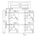
도 1의 (a) 내지 도 1의 (h)는 본 발명의 일 형태인 반도체 장치의 제작 방법의 일례를 도시하는 단면도.
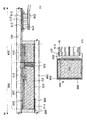
도 2의 (a) 내지 도 2의 (c)는 본 발명의 일 형태인 반도체 장치의 일례를 도시하는 상면도 및 단면도.
도 3의 (a) 내지 도 3의 (b)는 본 발명의 일 형태를 도시하는 회로도의 일례.
도 4는 본 발명의 일 형태를 도시하는 회로도의 일례.
도 5a 내지 도 5b는 본 발명의 일 형태를 도시하는 회로도의 일례.
도 6의 (a) 내지 도 6의 (b)는 본 발명의 일 형태를 도시하는 회로도의 일례.
도 7의 (a) 내지 도 7의 (c)는 CPU의 구체예를 도시하는 블록도 및 그 일부의 회로도.
도 8의 (a) 내지 도 8의 (b)는 본 발명의 일 형태를 나타내는 표시 장치의 일례를 도시하는 상면도 및 단면도.
도 9의 (a) 내지 도 9의 (b)는 본 발명의 일 형태를 나타내는 보호 회로의 일례를 도시하는 회로도 및 상면도.
도 10의 (a1), (a2), (b1), (b2), (c1), (c2)는 본 발명의 일 형태를 나타내는 액정의 동작 모드의 일례를 도시하는 단면도.
도 11의 (a1), (a2), (b1), (b2)는 본 발명의 일 형태를 나타내는 액정의 동작 모드의 일례를 도시하는 단면도.
도 12의 (a1), (a2), (b1), (b2)는 본 발명의 일 형태를 나타내는 액정의 동작 모드의 일례를 도시하는 단면도.
도 13의 (a) 내지 도 13의 (b)는 본 발명의 일 형태를 나타내는 액정의 동작 모드의 일례를 도시하는 상면도 및 단면도.
도 14의 (a) 내지 도 14의 (c)는 본 발명의 일 형태를 나타내는 액정의 동작 모드의 일례를 도시하는 상면도.
도 15의 (a) 내지 도 15의 (c)는 본 발명의 일 형태를 나타내는 액정의 동작 모드의 일례를 도시하는 상면도.
도 16의 (a) 내지 도 16의 (c)는 본 발명의 일 형태인 반도체 장치를 사용한 전자 기기의 예를 도시하는 사시도.
도 17은 본 발명의 일 형태를 설명하기 위한 결정의 모델.
도 18의 (a) 내지 도 18의 (c)는 본 발명의 일 형태를 설명하기 위한 결정의 모델.1A to 1H are cross-sectional views illustrating an example of a method of manufacturing a semiconductor device of one embodiment of the present invention.
2A to 2C are top views and cross-sectional views illustrating an example of a semiconductor device of one embodiment of the present invention.
3A to 3B are examples of a circuit diagram showing one embodiment of the present invention.
4 is an example of a circuit diagram showing one embodiment of the present invention.
5A to 5B are examples of circuit diagrams showing one embodiment of the present invention.
6A to 6B are examples of circuit diagrams showing one embodiment of the present invention.
7A to 7C are block diagrams showing specific examples of the CPU, and circuit diagrams of a part thereof.
8A to 8B are top views and cross-sectional views showing an example of the display device of one embodiment of the present invention.
9A to 9B are a circuit diagram and a top view showing an example of a protection circuit of one embodiment of the present invention.
(A1), (a2), (b1), (b2), (c1), (c2) is sectional drawing which shows an example of the operation mode of the liquid crystal which shows one form of this invention.
(A1), (a2), (b1), (b2) is sectional drawing which shows an example of the operation mode of the liquid crystal which shows one form of this invention.
(A1), (a2), (b1), (b2) is sectional drawing which shows an example of the operation mode of the liquid crystal which shows one form of this invention.
13A to 13B are top views and cross-sectional views showing examples of operation modes of the liquid crystal of one embodiment of the present invention.
14A to 14C are top views illustrating examples of operation modes of the liquid crystal of one embodiment of the present invention.
15A to 15C are top views illustrating examples of operation modes of the liquid crystal of one embodiment of the present invention.
16A to 16C are perspective views illustrating examples of electronic devices using the semiconductor device of one embodiment of the present invention.
Fig. 17 is a model of a crystal for explaining one embodiment of the present invention.
18A to 18C are models of crystals for explaining one embodiment of the present invention.
이하에서는 본 발명의 실시 형태에 대하여 도면을 사용하여 상세하게 설명한다. 단, 본 발명은 이하의 설명에 한정되지 않고, 그 형태 및 상세를 다양하게 변경할 수 있는 것은 당업자라면 용이하게 이해된다. 또한, 본 발명은 이하에 나타내는 실시 형태의 기재 내용에 한정하여 해석되는 것이 아니다. 또한, 도면을 사용하여 발명의 구성을 설명하는 데 있어서, 동일한 것을 가리키는 부호는 다른 도면간에서도 공통되게 사용한다. 또한, 동일한 것을 가리킬 때에는 해치 패턴을 동일하게 하고, 특별히 부호를 붙이지 않는 경우가 있다.EMBODIMENT OF THE INVENTION Hereinafter, embodiment of this invention is described in detail using drawing. However, this invention is not limited to the following description, It is easily understood by those skilled in the art that various forms and details can be changed. In addition, this invention is not interpreted limited to description content of embodiment shown below. In addition, in describing the structure of the invention using the drawings, the same reference numerals are used in common among different drawings. In addition, when referring to the same thing, a hatch pattern may be made the same and a code | symbol may not be specifically attached.
이하, 본 발명의 설명을 행하는데, 본 명세서에서 사용하는 용어에 대하여 간단하게 설명한다. 우선, 트랜지스터의 소스와 드레인에 대해서는, 본 명세서에 있어서는 한쪽을 드레인이라고 칭할 때 다른쪽을 소스로 한다. 즉, 전위의 고저에 의해 그것들을 구별하지 않는다. 따라서, 본 명세서에 있어서 소스로 되어 있는 부분을 드레인으로 바꾸어 읽을 수도 있다.EMBODIMENT OF THE INVENTION Hereafter, although this invention is demonstrated, the term used by this specification is demonstrated easily. First, the source and the drain of a transistor are referred to as a drain in this specification when the other is a source. That is, they are not distinguished by the level of potential. Therefore, in this specification, the part used as a source can also be read as a drain.
또한, 전압은 어떤 전위와 기준의 전위(예를 들어 접지 전위)의 전위차를 나타내는 경우가 많다. 따라서, 전압을 전위로 바꾸어 말하는 것이 가능하다.In addition, the voltage often shows a potential difference between a potential and a reference potential (for example, a ground potential). Thus, it is possible to change the voltage into a potential.
본 명세서에 있어서는 「접속한다」라고 표현되는 경우라도 현실의 회로에 있어서는 물리적인 접속 부분이 없고, 배선이 연장되어 있을 뿐인 경우도 있다.In this specification, even when it is expressed as "connecting", in a real circuit, there is no physical connection part and the wiring may only be extended.
또한, 제1, 제2로서 부여되는 서수사는 편의상 사용하는 것이며, 공정순 또는 적층순을 나타내는 것이 아니다. 또한, 본 명세서에 있어서 발명을 특정하기 위한 사항으로서 고유의 명칭을 나타내는 것이 아니다.In addition, the ordinal numbers given as 1st and 2nd are used for convenience, and do not represent a process order or lamination order. In addition, in this specification, as a matter for specifying invention, the original name is not shown.
(실시 형태 1)(Embodiment 1)
본 실시 형태에서는 본 발명의 일 형태의 반도체 장치 및 그 제작 방법에 대하여 상면도 및 단면도를 사용하여 설명한다.In this embodiment, a semiconductor device of one embodiment of the present invention and a manufacturing method thereof will be described using a top view and a cross-sectional view.
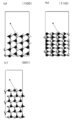
도 2의 (a) 내지 도 2의 (c)는 본 발명의 일 형태인 반도체 장치이다. 도 2의 (a)는 반도체 장치의 상면도이고, 도 2의 (b) 및 도 2의 (c)는 각각 도 2의 (a)의 일점쇄선 A-B 및 일점쇄선 C-D에서의 단면도이다.2A to 2C are semiconductor devices of one embodiment of the present invention. FIG. 2A is a top view of the semiconductor device, and FIGS. 2B and 2C are cross-sectional views taken along the dashed-dotted line A-B and the dashed-dotted line C-D of FIG. 2A, respectively.
도 2의 (a)는 간단화를 위하여 일부의 막을 생략하여 도시한다.2 (a) shows a part of the film is omitted for simplicity.
도 2의 (a)에 있어서, 소스 전극 및 드레인 전극(118)과 산화물 반도체막(126)은 일부의 상면 형상이 개략적으로 일치되어 있다. 바꾸어 말하면, 소스 전극 및 드레인 전극(118)은 그 모든 영역에 있어서 산화물 반도체막(126)과 중첩한다.In FIG. 2A, the top and bottom surfaces of the source electrode and
「상면 형상이 개략적으로 일치」란, 적층한 막과 막의 사이에서 적어도 일부의 윤곽이 겹쳐 직선 또는 곡선을 형성하는 것을 말한다. 단, 윤곽이 서로 겹치지 않고 상층의 막이 하층의 막의 내측에 형성되는 것이나 상층의 막이 하층의 막의 외측에 형성되는 경우도 있으며, 이 경우에도 「상면 형상이 개략적으로 일치」라고 한다."Upper surface shape is substantially coincident" means that at least one outline overlaps between the laminated film and the film to form a straight line or curve. However, the contours do not overlap each other, and the upper layer film is formed inside the lower layer film, and the upper layer film may be formed outside the lower layer film.
도 2의 (b)에 대하여 설명한다. 도 2의 (b)는 기판(100)과, 기판(100) 위의 하지 절연막(102)과, 하지 절연막(102) 위의 제1 영역(136) 및 제2 영역(146)을 포함하는 산화물 반도체막(126)과, 산화물 반도체막(126) 위의 소스 전극 및 드레인 전극(118)과, 소스 전극 및 드레인 전극(118) 및 산화물 반도체막(126) 위의 게이트 절연막(112)과, 게이트 절연막(112) 위의 게이트 전극(104)과, 게이트 절연막(112) 및 게이트 전극(104) 위의 층간 절연막(122)을 갖는 구조를 도시한다.2 (b) will be described. 2B illustrates an oxide including a
이어서, 도 2의 (c)에 대하여 설명한다. 도 2의 (c)는 기판(100)과, 기판(100) 위의 하지 절연막(102)과, 하지 절연막(102) 위의 산화물 반도체막(126)의 제1 영역(136)과, 하지 절연막(102) 및 산화물 반도체막(126)을 덮는 게이트 절연막(112)과, 게이트 절연막(112) 위의 게이트 전극(104)과, 게이트 전극(104) 위의 층간 절연막(122)을 갖는 구조를 도시한다.Next, FIG. 2C is described. 2C shows a
이어서, 도 2의 (a) 내지 도 2의 (c)에 도시하는 반도체 장치의 제작 방법에 대하여 도 1의 (a) 내지 도 1의 (h)를 사용하여 설명한다.Next, the manufacturing method of the semiconductor device shown to FIG.2 (a)-FIG.2 (c) is demonstrated using FIG.1 (a)-FIG.1 (h).
우선, 기판(100) 위에 하지 절연막(102) 및 제1 산화물 반도체막(106)을 이 순서대로 형성한다(도 1의 (a) 참조).First, the
기판(100)에 큰 제한은 없지만, 적어도 후속 열처리에 견딜 수 있을 정도의 내열성을 갖고 있을 필요가 있다. 예를 들어, 유리 기판, 세라믹 기판, 석영 기판, 사파이어 기판 등을 기판(100)으로서 사용하여도 된다. 또한, 실리콘이나 탄화실리콘 등의 단결정 반도체 기판, 다결정 반도체 기판, 실리콘 게르마늄 등의 화합물 반도체 기판, SOI(Silicon On Insulator) 기판 등을 적용할 수 있고, 이들 기판 위에 반도체 소자가 설치된 것을 기판(100)으로서 사용하여도 된다.Although there is no big limitation in the board |
또한, 기판(100)으로서 가요성 기판을 사용하여도 된다. 그 경우에는 가요성 기판 위에 직접적으로 트랜지스터를 제작하게 된다. 또한, 가요성 기판 위에 트랜지스터를 설치하기 위해서는 기판(100)으로서 비가요성의 것을 사용하여 이 위에 트랜지스터를 제작한 후, 트랜지스터를 박리하여 가요성 기판에 전치하는 방법도 있다. 그 경우에는 기판(100)과 트랜지스터의 사이에 박리층을 형성하면 된다.In addition, a flexible substrate may be used as the
하지 절연막(102)은, 예를 들어 산화실리콘, 산화질화실리콘, 질화산화실리콘, 질화실리콘, 산화알루미늄, 산화하프늄, 산화이트륨 또는 산화지르코늄 등을 사용하면 되며, 적층 또는 단층으로 설치한다. 예를 들어, 열산화법, CVD법, 스퍼터링법 등으로 형성하면 된다. 하지 절연막(102)은 가열 처리에 의해 산소를 방출하는 막을 사용하여도 된다. 가열 처리에 의해 산소를 방출하는 막을 사용함으로써 제1 산화물 반도체막(106)에 발생하는 결함을 수복할 수 있고, 트랜지스터의 전기 특성을 향상시킬 수 있다.The base
여기서, 산화질화실리콘은 실리콘, 산소 및 질소를 포함하고, 또한 질소보다도 산소의 함유량이 많은 것을 가리킨다. 또한, 질화산화실리콘은 실리콘, 산소 및 질소를 포함하고, 또한 산소보다도 질소의 함유량이 많은 것을 가리킨다.Here, silicon oxynitride contains silicon, oxygen, and nitrogen, and points out that oxygen content is larger than nitrogen. In addition, silicon nitride oxide contains silicon, oxygen, and nitrogen, and points out that nitrogen content is larger than oxygen.
하지 절연막(102)은 트랜지스터 특성에 악영향을 주는 원소가 기판(100)으로부터 제1 산화물 반도체막(106)으로 확산되는 것을 방지하기 위하여 설치된다. 따라서, 하지 절연막(102)은 전술한 원소의 확산 계수가 작은 절연막을 사용하면 된다. 이것은 이하에 나타내는 게이트 절연막(112) 및 층간 절연막(122)도 마찬가지이다.The underlying
「가열 처리에 의해 산소를 방출하는」이란, TDS(Thermal Desorption Spectroscopy: 온도 상승 탈리 가스 분광법) 분석에 의해 방출되는 산소가 산소 원자로 환산하여 1.0×10¹⁸atoms/cm3 이상, 또는 3.0×10²⁰atoms/cm3 이상인 것을 말한다.The term “releasing oxygen by heating” means that oxygen released by TDS (Thermal Desorption Spectroscopy) analysis is converted into oxygen atoms and converted to oxygen atoms in a range of 1.0 × 10 18 atoms / cm 3 or more, or 3.0 × 10 20. It means that it is more than atoms / cm < 3 >.
여기서, TDS 분석을 사용한 산소의 방출량의 측정 방법에 대하여 이하에 설명한다.Here, the measuring method of the amount of oxygen released | released using TDS analysis is demonstrated below.
TDS 분석을 하였을 때의 기체의 전체 방출량은 방출 가스의 이온 강도의 적분값에 비례한다. 그리고, 이 적분값과 표준 시료의 비교에 의해 기체의 전체 방출량을 계산할 수 있다.The total amount of gas released in the TDS analysis is proportional to the integral value of the ionic strength of the released gas. And the total discharge amount of gas can be calculated by comparison of this integral value and a standard sample.
예를 들어, 표준 시료인 소정의 밀도의 수소를 포함하는 실리콘 웨이퍼의 TDS 분석 결과 및 절연막의 TDS 분석 결과로부터, 절연막의 산소 분자의 방출량(NO2)은 수학식 1에 의해 구할 수 있다. 여기서, TDS 분석에 의해 얻어지는 질량수 32에서 검출되는 가스 모두가 산소 분자 유래라고 가정한다. 질량수 32의 것으로서 그 밖에 CH3OH가 있지만, 존재할 가능성이 낮은 것으로서 여기에서는 고려하지 않는다. 또한, 산소 원자의 동위체인 질량수 17의 산소 원자 및 질량수 18의 산소 원자를 포함하는 산소 분자에 대해서도 자연계에서의 존재 비율이 극미량이기 때문에 고려하지 않는다.For example, from the TDS analysis result of the silicon wafer containing hydrogen of a predetermined density which is a standard sample, and the TDS analysis result of the insulating film, the amount of oxygen molecules released from the insulating film (NO 2 ) can be calculated by Equation (1). Here, it is assumed that all the gases detected at the mass number 32 obtained by TDS analysis are derived from oxygen molecules. There is CH 3 OH in addition to the mass number 32, but it is not considered here as it is unlikely to exist. In addition, oxygen molecules containing an oxygen atom with a mass number of 17 and an oxygen atom with a mass number of 18, which are isotopes of oxygen atoms, are not considered because of their extremely small proportion in nature.
![]()
![]()
식 중, NH2는 표준 시료로부터 탈리한 수소 분자를 밀도에 의해 환산한 값이다. SH2는 표준 시료를 TDS 분석하였을 때의 이온 강도의 적분값이다. 여기서, 표준 시료의 기준값을 NH2/SH2로 한다. SO2는 절연막을 TDS 분석하였을 때의 이온 강도의 적분값이다. α는 TDS 분석에서의 이온 강도에 영향을 미치는 계수이다. 수학식 1의 상세에 관해서는 일본 특허 공개 평6-275697호 공보를 참조한다. 또한, 상기 절연막의 산소의 방출량은 덴시 가가꾸 가부시끼가이샤제의 온도 상승 탈리 분석 장치 EMD-WA1000S/W를 사용하고, 표준 시료로서 1×10¹⁶atoms/cm3의 수소 원자를 포함하는 실리콘 웨이퍼를 사용하여 측정하였다.In the formula, N H2 is a value obtained by converting the hydrogen molecules released from the standard sample by density. S H2 is the integral value of the ionic strength when the standard sample is analyzed by TDS. Here, the reference value of the standard sample is N H2 / S H2 . S O2 is an integral value of the ionic strength when the insulating film is analyzed by TDS. α is a coefficient that affects the ionic strength in the TDS analysis. For the details of
또한, TDS 분석에 있어서, 산소의 일부는 산소 원자로서 검출된다. 산소 분자와 산소 원자의 비율은 산소 분자의 이온화율로부터 산출할 수 있다. 또한, 상술한 α는 산소 분자의 이온화율을 포함하기 때문에, 산소 분자의 방출량을 평가함으로써 산소 원자의 방출량에 대해서도 어림잡을 수 있다.In addition, in TDS analysis, part of oxygen is detected as an oxygen atom. The ratio of oxygen molecules and oxygen atoms can be calculated from the ionization rate of the oxygen molecules. In addition, since alpha mentioned above contains the ionization rate of an oxygen molecule, the emission amount of an oxygen atom can be estimated also by evaluating the emission amount of an oxygen molecule.
또한, NO2는 산소 분자의 방출량이다. 산소 원자로 환산하였을 때의 방출량은 산소 분자의 방출량의 2배로 된다.In addition, N O2 is the amount of oxygen molecules released. The emission amount in terms of oxygen atoms is twice that of oxygen molecules.
상기 구성에 있어서, 가열 처리에 의해 산소를 방출하는 막은 산소가 과잉인 산화실리콘(SiOX(X>2))이어도 된다. 산소가 과잉인 산화실리콘(SiOX(X>2))은 실리콘 원자수의 2배보다 많은 산소 원자를 단위 체적당 포함하는 것이다. 단위 체적당 실리콘 원자수 및 산소 원자수는 러더퍼드 후방 산란법에 의해 측정한 값이다.In the above configuration, the film that releases oxygen by heat treatment may be silicon oxide (SiO X (X> 2)) in which oxygen is excessive. Silicon oxide with an excess of oxygen (SiO X (X> 2)) contains more than twice as many oxygen atoms per unit volume of silicon atoms. The number of silicon atoms and oxygen atoms per unit volume is the value measured by Rutherford backscattering method.
하지 절연막(102)으로부터 제1 산화물 반도체막(106)에 산소가 공급됨으로써, 제1 산화물 반도체막(106)과 하지 절연막(102)의 계면 준위를 저감할 수 있다. 이 결과, 트랜지스터의 동작 등에 기인하여 제1 산화물 반도체막(106)과 하지 절연막(102)의 계면에 캐리어가 포획되는 것을 억제할 수 있어, 트랜지스터의 전기 특성을 향상시킬 수 있다.By supplying oxygen from the underlying insulating
또한, 산화물 반도체막의 산소 결손에 기인하여 전하가 발생하는 경우가 있다. 일반적으로 산화물 반도체막의 산소 결손은, 그 일부가 도너로 되어 캐리어인 전자를 방출한다. 이 결과, 트랜지스터의 임계값 전압이 마이너스 방향으로 시프트하게 된다. 하지 절연막(102)으로부터 제1 산화물 반도체막(106)에 산소가 충분히 공급됨으로써, 임계값 전압이 마이너스 방향으로 시프트하는 요인인, 산화물 반도체막의 산소 결손을 저감할 수 있다.In addition, charges may occur due to oxygen vacancies in the oxide semiconductor film. In general, oxygen vacancies in the oxide semiconductor film are partially donors and emit electrons as carriers. As a result, the threshold voltage of the transistor is shifted in the negative direction. By sufficiently supplying oxygen to the first
즉, 하지 절연막(102)에 가열 처리에 의해 산소를 방출하는 막을 설치함으로써, 제1 산화물 반도체막(106)과 하지 절연막(102)의 계면에서의 계면 준위 및 제1 산화물 반도체막(106)의 산소 결손을 저감하여, 제1 산화물 반도체막(106)과 하지 절연막(102)의 계면에서의 캐리어 포획의 영향을 작게 할 수 있다.That is, by providing a film that releases oxygen by heat treatment in the underlying insulating
이상으로 하지 절연막(102)으로부터 발휘되는 효과를 나타내었지만, 적절하게 하지 절연막(102)을 게이트 절연막(112) 및 층간 절연막(122)으로 치환하여도 된다. 그 경우, 효과를 발휘하는 공정에 의거하여, 제1 산화물 반도체막(106)을 제2 산화물 반도체막(116) 또는 산화물 반도체막(126)으로 치환하면 된다.Although the effect exerted from the
제1 산화물 반도체막(106)으로서 CAAC 산화물 반도체(C Axis Aligned Crystalline Oxide Semiconductor라고도 함)를 사용하면 바람직하다. 단, 제1 산화물 반도체막(106)은 CAAC 산화물 반도체에 한정되는 것이 아니며, 비정질 산화물 반도체막을 사용하여도 된다.It is preferable to use CAAC oxide semiconductor (also called C Axis Aligned Crystalline Oxide Semiconductor) as the first
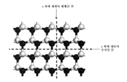
CAAC 산화물 반도체는 c축 배향하고, 또한 ab면, 표면 또는 계면의 방향으로부터 보아 삼각 형상 또는 육각 형상의 원자 배열을 갖고, c축에 있어서는 금속 원자가 층상 또는 금속 원자와 산소 원자가 층 위로 배열되어 있고, ab면(또는 표면 또는 계면)에 있어서는 a축 또는 b축의 방향이 다른(c축을 중심으로 회전한) 결정을 포함하는 산화물 반도체를 말한다.The CAAC oxide semiconductor has a c-axis orientation and has a triangular or hexagonal atomic arrangement as viewed from the ab plane, surface or interface direction, and in the c axis, the metal atoms are layered or the metal atoms and oxygen atoms are arranged on the layer. An ab semiconductor (or surface or interface) refers to an oxide semiconductor containing crystals (rotated about a c axis) different in the a-axis or b-axis direction.
광의로 CAAC 산화물 반도체는 비단결정이며, 그 ab면에 수직인 방향으로부터 보아 삼각형 혹은 육각형, 또는 정삼각형 혹은 정육각형의 원자 배열을 갖고, 또한 c축에 수직인 방향으로부터 보아 금속 원자가 층상 또는 금속 원자와 산소 원자가 층 위로 배열된 상을 포함하는 재료를 말한다.Broadly speaking, CAAC oxide semiconductors are non-single crystals, and have a triangular or hexagonal or equilateral triangle or hexagonal atomic arrangement viewed from the direction perpendicular to the ab plane, and the metal atoms are layered or metal atoms and oxygen viewed from the direction perpendicular to the c-axis. Refers to a material comprising a phase in which atoms are arranged over the layer.
CAAC 산화물 반도체는 단결정은 아니지만, 비정질만으로 형성되어 있는 것도 아니다. 또한, CAAC 산화물 반도체는 결정화한 부분(결정 부분)을 포함하지만, 1개의 결정 부분과 다른 결정 부분의 경계를 명확하게 판별하지 못하는 경우도 있다.Although the CAAC oxide semiconductor is not single crystal, it is not formed only amorphous. In addition, although the CAAC oxide semiconductor includes a crystallized portion (crystal portion), in some cases, the boundary between one crystal portion and another crystal portion cannot be clearly determined.
CAAC 산화물 반도체를 구성하는 산소의 일부는 질소에 의해 치환되어도 된다. 또한, CAAC 산화물 반도체를 구성하는 개개의 결정 부분의 c축은 일정한 방향(예를 들어, CAAC 산화물 반도체를 지지하는 기판면이나 CAAC 산화물 반도체의 표면에 수직인 방향)으로 정렬되어도 된다. 또는 CAAC 산화물 반도체를 구성하는 개개의 결정 부분의 ab면의 법선은 일정한 방향(예를 들어, CAAC 산화물 반도체를 지지하는 기판면이나 CAAC 산화물 반도체의 표면에 수직인 방향)을 향하고 있어도 된다.A part of oxygen which comprises a CAAC oxide semiconductor may be substituted by nitrogen. In addition, the c-axis of the individual crystal parts constituting the CAAC oxide semiconductor may be aligned in a constant direction (for example, in a direction perpendicular to the surface of the substrate supporting the CAAC oxide semiconductor or the surface of the CAAC oxide semiconductor). Alternatively, the normal line of the ab planes of the individual crystal parts constituting the CAAC oxide semiconductor may be directed in a predetermined direction (for example, a substrate surface supporting the CAAC oxide semiconductor or a direction perpendicular to the surface of the CAAC oxide semiconductor).
CAAC 산화물 반도체는 그 조성 등에 따라 도체 또는 절연체로 될 수 있다. 또한, 그 조성 등에 따라 가시광에 대하여 투명하거나 불투명하거나 한다.The CAAC oxide semiconductor may be a conductor or an insulator depending on its composition and the like. Further, the composition may be transparent or opaque to visible light depending on the composition and the like.
이어서, CAAC 산화물 반도체의 형성 방법에 대하여 설명한다.Next, the formation method of a CAAC oxide semiconductor is demonstrated.
우선, 산화물 반도체막을 스퍼터링법, 분자선 에피택시법, 원자층 퇴적법 또는 펄스 레이저 증착법에 의해 형성한다. 또한, 형성 시에 기판을 가열 처리함으로써 결정 영역의 비율이 많은 산화물 반도체막으로 할 수 있다. 예를 들어, 기판 온도가 150℃ 이상 450℃ 이하로 하면 되고, 바람직하게는 기판 온도가 200℃ 이상 350℃ 이하로 한다.First, an oxide semiconductor film is formed by sputtering, molecular beam epitaxy, atomic layer deposition, or pulsed laser deposition. In addition, by heat-processing a board | substrate at the time of formation, it can be set as the oxide semiconductor film with many ratios of a crystal region. For example, the substrate temperature may be 150 ° C or more and 450 ° C or less, and preferably, the substrate temperature is 200 ° C or more and 350 ° C or less.
이어서, 제1 가열 처리를 행하여도 된다. 제1 가열 처리를 행함으로써 보다 결정 영역의 비율이 높은 산화물 반도체막을 형성할 수 있다. 제1 가열 처리는, 예를 들어 200℃ 이상 기판의 왜곡점 미만에서 행하면 된다. 바람직하게는 250℃ 이상 450℃ 이하로 한다. 분위기는 한정되지 않지만, 산화성 분위기, 불활성 분위기 또는 감압 분위기에서 행한다. 처리 시간은 3분 내지 24시간으로 한다. 처리 시간을 길게 할 수록 결정 영역의 비율이 높은 산화물 반도체막을 형성할 수 있지만, 24시간을 초과하는 열처리는 생산성의 저하를 초래하기 때문에 바람직하지 않다.Subsequently, you may perform a 1st heat processing. By performing the first heat treatment, an oxide semiconductor film having a higher ratio of crystal regions can be formed. What is necessary is just to perform a 1st heat processing below 200 degreeC of distortion points of a board | substrate, for example. Preferably, you may be 250 degreeC or more and 450 degrees C or less. The atmosphere is not limited, but is performed in an oxidizing atmosphere, an inert atmosphere or a reduced pressure atmosphere. The treatment time is 3 minutes to 24 hours. An oxide semiconductor film having a higher ratio of crystal regions can be formed with a longer processing time, but heat treatment over 24 hours is not preferable because it causes a decrease in productivity.
산화성 분위기는 산화성 가스를 포함하는 분위기이다. 산화성 가스는 산소, 오존 또는 아산화질소 등이며, 물, 수소 등이 포함되지 않는 것이 바람직하다. 예를 들어, 열처리 장치에 도입하는 산소, 오존, 아산화질소의 순도를 8N(99.999999%) 이상, 바람직하게는 9N(99.9999999%) 이상(불순물 농도가 10ppb 이하, 바람직하게는 0.1ppb 미만)으로 한다. 산화성 분위기는 산화성 가스를 불활성 가스와 혼합하여 사용하여도 된다. 그 경우, 산화성 가스가 적어도 10ppm 이상 포함되는 분위기로 한다.The oxidative atmosphere is an atmosphere containing an oxidizing gas. The oxidizing gas is oxygen, ozone, nitrous oxide, or the like, and preferably does not contain water, hydrogen, or the like. For example, the purity of oxygen, ozone and nitrous oxide introduced into the heat treatment apparatus is 8N (99.999999%) or more, preferably 9N (99.9999999%) or more (impurity concentration is 10ppb or less, preferably 0.1ppb or less). . The oxidizing atmosphere may be used by mixing an oxidizing gas with an inert gas. In that case, it is set as the atmosphere containing at least 10 ppm or more of oxidizing gas.
여기서, 불활성 분위기는 질소, 희가스(헬륨, 네온, 아르곤, 크립톤, 크세논) 등의 불활성 가스를 주성분으로 하는 분위기이다. 구체적으로는 산화성 가스 등의 반응성 가스가 10ppm 미만인 분위기로 한다.Here, an inert atmosphere is an atmosphere which has an inert gas, such as nitrogen and a rare gas (helium, neon, argon, krypton, xenon) as a main component. Specifically, an atmosphere having a reactive gas such as an oxidizing gas is less than 10 ppm.
제1 가열 처리는 RTA(Rapid Thermal Anneal) 장치를 사용할 수 있다. RTA를 사용함으로써 단시간에 한하여 기판의 왜곡점 이상의 온도에서 열처리를 행할 수 있다. 그로 인해, 비정질 영역에 대하여 결정 영역의 비율이 많은 산화물 반도체막을 형성하기 위한 시간을 단축할 수 있다.The first heat treatment may use a Rapid Thermal Anneal (RTA) device. By using RTA, heat treatment can be performed at a temperature higher than the strain point of the substrate for a short time. Therefore, the time for forming the oxide semiconductor film with a large ratio of crystal region with respect to an amorphous region can be shortened.
산화물 반도체막으로서는 4원계 금속 산화물인 In-Sn-Ga-Zn-O계의 재료나, 3원계 금속 산화물인 In-Ga-Zn-O계의 재료, In-Sn-Zn-O계의 재료, In-Al-Zn-O계의 재료, Sn-Ga-Zn-O계의 재료, Al-Ga-Zn-O계의 재료, Sn-Al-Zn-O계의 재료나, 2원계 금속 산화물인 In-Zn-O계의 재료, Sn-Zn-O계의 재료, Al-Zn-O계의 재료, Zn-Mg-O계의 재료, Sn-Mg-O계의 재료, In-Mg-O계의 재료, In-Ga-O계의 재료나, In-O계의 재료, Sn-O계의 재료, Zn-O계의 재료 등을 사용하여도 된다. 또한, 상기의 재료에 산화실리콘을 포함시켜도 된다. 여기서, 예를 들어 In-Ga-Zn-O계의 재료는 인듐(In), 갈륨(Ga), 아연(Zn)을 갖는 산화물이라고 하는 의미이며, 그 조성비는 특별히 상관없다. 또한, In과 Ga와 Zn 이외의 원소를 포함하여도 된다. 이때, 산화물 반도체막의 화학양론비에 대하여 O를 과잉으로 하면 바람직하다. O를 과잉으로 함으로써 산화물 반도체막의 산소 결손에 기인하는 캐리어의 생성을 억제할 수 있다.As the oxide semiconductor film, an In-Sn-Ga-Zn-O-based material which is a quaternary metal oxide, an In-Ga-Zn-O-based material which is a ternary metal oxide, an In-Sn-Zn-O-based material, In-Al-Zn-O-based material, Sn-Ga-Zn-O-based material, Al-Ga-Zn-O-based material, Sn-Al-Zn-O-based material or binary metal oxide In-Zn-O-based material, Sn-Zn-O-based material, Al-Zn-O-based material, Zn-Mg-O-based material, Sn-Mg-O-based material, In-Mg-O You may use a system material, an In-Ga-O type material, an In-O type material, a Sn-O type material, a Zn-O type material, etc. Moreover, you may contain a silicon oxide in said material. Here, for example, an In—Ga—Zn—O-based material is referred to as an oxide having indium (In), gallium (Ga), and zinc (Zn), and the composition ratio thereof does not matter in particular. In addition, elements other than In, Ga, and Zn may be included. At this time, it is preferable to make O excess with respect to the stoichiometric ratio of an oxide semiconductor film. By making O excess, the production | generation of the carrier resulting from the oxygen deficiency of an oxide semiconductor film can be suppressed.
또한, 일례로서 산화물 반도체막으로서 In-Zn-O계의 재료를 사용하는 경우, 원자수비로 In/Zn=0.5 내지 50, 바람직하게는 In/Zn=1 내지 20, 더욱 바람직하게는 In/Zn=3 내지 15로 한다. Zn의 원자수비를 전술한 범위로 함으로써 트랜지스터의 전계 효과 이동도를 향상시킬 수 있다. 여기서, 화합물의 원자수비가 In:Zn:O=X:Y:Z일 때, Z>1.5X+Y로 한다.In the case of using an In—Zn—O-based material as an oxide semiconductor film as an example, In / Zn = 0.5 to 50, preferably In / Zn = 1 to 20, and more preferably In / Zn in atomic ratio = 3 to 15. By setting the atomic ratio of Zn to the above-described range, the field effect mobility of the transistor can be improved. Here, when the atomic number ratio of the compound is In: Zn: O = X: Y: Z, let Z> 1.5X + Y.
산화물 반도체막으로서 화학식 InMO3(ZnO)m(m>0)으로 표기되는 재료를 사용하여도 된다. 여기서, M은 Ga, Al, Mn 및 Co로부터 선택된 1개 또는 복수의 금속 원소를 나타낸다. 예를 들어, M으로서 Ga, Ga 및 Al, Ga 및 Mn 또는 Ga 및 Co 등을 사용하여도 된다.As the oxide semiconductor film, a material represented by the chemical formula InMO 3 (ZnO) m (m> 0) may be used. Here, M represents one or a plurality of metal elements selected from Ga, Al, Mn and Co. For example, Ga, Ga and Al, Ga and Mn, or Ga and Co may be used as M.
또한, 질소를 1×10¹⁷atoms/cm3 이상 5×10¹⁹atoms/cm3 이하(바람직하게는 5×10¹⁸atoms/cm3 이하) 포함하는 In-Ga-Zn-O계의 재료는 c축 배향된 육방정의 결정 구조를 포함하는 산화물로 되고, In-O의 결정면(인듐과 산소를 포함하는 결정면)과 In-O의 결정면(인듐과 산소를 포함하는 결정면)의 사이에 1층의 Ga 및 Zn을 갖는 층을 구비한다. 또는, 상술한 범위에서 질소를 포함하는 In-Ga-Zn-O계의 산화물 반도체막에 있어서, 인접하는 In-O의 결정면과 In-O의 결정면의 사이에 복수층의 Ga 및 Zn을 갖는 층을 구비하여도 상관없다.The In-Ga-Zn-O-based material containing nitrogen in an amount of 1 × 10 17 atoms / cm 3 or more and 5 × 10 19 atoms / cm 3 or less (preferably 5 × 10 18 atoms / cm 3 or less) is c. 1 layer of Ga between an axially oriented hexagonal crystal structure and an In-O crystal surface (crystal surface containing indium and oxygen) and In-O crystal surface (crystal surface containing indium and oxygen) And a layer having Zn. Alternatively, in the In-Ga-Zn-O-based oxide semiconductor film containing nitrogen in the above-described range, a layer having a plurality of layers of Ga and Zn between adjacent In-O crystal surfaces and In-O crystal surfaces. It may be provided.
이어서, 산화물 반도체막 위에 2층째의 산화물 반도체막을 형성하여, 산화물 반도체막의 적층체를 형성하여도 된다. 1층째의 산화물 반도체막과 2층째의 산화물 반도체막은 마찬가지의 방법으로 형성할 수 있다.Subsequently, the second oxide semiconductor film may be formed on the oxide semiconductor film to form a laminate of the oxide semiconductor film. The oxide semiconductor film of the first layer and the oxide semiconductor film of the second layer can be formed by the same method.
2층째의 산화물 반도체막을 형성할 때, 기판을 가열 처리하면서 형성함으로써, 1층째의 산화물 반도체막을 종결정으로 2층째의 산화물 반도체막을 결정화시킬 수 있다. 이때, 1층째의 산화물 반도체막과 2층째의 산화물 반도체막이 동일한 원소로 구성되는 것을 호모 성장이라고 한다. 또는 1층째의 산화물 반도체막과 2층째의 산화물 반도체막이 적어도 1종 이상 다른 원소로 구성되는 것을 헤테로 성장이라고 한다.When forming the oxide semiconductor film of the second layer, the oxide semiconductor film of the first layer can be crystallized by the seed crystal of the oxide semiconductor film of the first layer by forming the substrate while heating the substrate. At this time, it is called homo growth that an oxide semiconductor film of a 1st layer and an oxide semiconductor film of a 2nd layer consist of the same element. Or it is called hetero growth that an oxide semiconductor film of a 1st layer and an oxide semiconductor film of a 2nd layer consist of at least 1 type or more of other elements.
또한, 2층째의 산화물 반도체막을 형성한 후, 제2 가열 처리를 행하여도 된다. 제2 가열 처리는 제1 가열 처리와 마찬가지의 방법으로 행하면 된다. 제2 가열 처리를 행함으로써, 비정질 영역에 대하여 결정 영역의 비율이 많은 적층 구조로 할 수 있다. 또는, 제2 가열 처리를 행함으로써, 1층째의 산화물 반도체막을 종결정으로 2층째의 산화물 반도체막을 결정화시킬 수 있다. 이때, 1층째의 산화물 반도체막과 2층째의 산화물 반도체막이 동일한 원소로 구성되는 호모 성장으로 하여도 상관없다. 또는 1층째의 산화물 반도체막과 2층째의 산화물 반도체막이 적어도 1종 이상 다른 원소로 구성되는 헤테로 성장으로 하여도 상관없다.In addition, after forming the second oxide semiconductor film, the second heat treatment may be performed. What is necessary is just to perform a 2nd heat processing by the method similar to a 1st heat processing. By performing a 2nd heat processing, it can be set as the laminated structure with many ratios of a crystalline region with respect to an amorphous region. Alternatively, by performing the second heat treatment, the oxide semiconductor film of the second layer can be crystallized by using the first oxide semiconductor film as a seed crystal. At this time, the oxide semiconductor film of the first layer and the oxide semiconductor film of the second layer may be homogeneous growths composed of the same element. Alternatively, the oxide semiconductor film of the first layer and the oxide semiconductor film of the second layer may be hetero growths composed of at least one or more different elements.
이상의 방법에 의해 CAAC 산화물 반도체를 형성할 수 있다.A CAAC oxide semiconductor can be formed by the above method.
여기서, CAAC 산화물 반도체를 형성하는 과정의 제1 가열 처리 및 제2 가열 처리에 의해, 하지 절연막(102)으로부터 제1 산화물 반도체막(106)에 산소를 공급하여도 상관없다.Here, oxygen may be supplied from the
제1 산화물 반도체막(106)을 형성한 후, 제3 가열 처리를 행하여도 상관없다. 제3 가열 처리는 150℃ 이상 기판의 왜곡점 미만, 바람직하게는 250℃ 이상 450℃ 이하, 더욱 바람직하게는 300℃ 이상 450℃ 이하의 온도에서 행한다. 제3 가열 처리에 의해 하지 절연막(102)으로부터 제1 산화물 반도체막(106)에 산소를 공급할 수 있다. 제3 가열 처리는 감압 분위기, 불활성 분위기 또는 산화성 분위기에서 행한다.After forming the 1st
이어서, 제1 산화물 반도체막(106) 위에 도전막(108)을 형성한다(도 1의 (b) 참조).Next, a
도전막(108)은 단층 또는 적층 구조로 하면 되며, Al, Ti, Cr, Co, Ni, Cu, Y, Zr, Mo, Ag, Ta 및 W, 그들의 질화물, 산화물 및 합금으로부터 1개 이상 선택하여 사용하면 된다. 산화물 도전막은 금속막과 비교하여 저항이 높기 때문에, 도전막(108)의 저항을 저감하기 위하여 시트 저항이 10Ω/sq 이하인 저저항막과 적층하면 바람직하다.The
도전막(108)을 형성한 후, 제4 가열 처리를 행하여도 상관없다. 제4 가열 처리는 제3 가열 처리와 마찬가지의 방법으로 행하면 된다. 제4 가열 처리에 의해 하지 절연막(102)으로부터 제1 산화물 반도체막(106)에 산소를 공급할 수 있다.After the
이어서, 도전막(108) 위에 레지스트를 도포하고, 포토리소그래피법에 의해 레지스트 마스크를 형성한다. 상기 레지스트 마스크를 사용하여 도전막(108)을 가공하여 소스 전극 및 드레인 전극(118)을 형성한다(도 1의 (c) 참조).Next, a resist is apply | coated on the
이어서, 제1 산화물 반도체막(106) 위에 레지스트를 도포하고, 포토리소그래피법에 의해 레지스트 마스크를 형성한다. 상기 레지스트 마스크를 사용하여 제1 산화물 반도체막(106)을 가공하여 제2 산화물 반도체막(116)을 형성한다(도 1의 (d) 참조). 이에 의해, 소스 전극 및 드레인 전극(118)의 저면이 제2 산화물 반도체막(116)의 측면과 접하는 것을 방지할 수 있다.Next, a resist is apply | coated on the 1st
또는 도전막(108) 및 제1 산화물 반도체막(106)을 다계조 마스크에 의해 형성한 레지스트 마스크를 사용하여 가공하여도 된다. 이 경우, 다계조 마스크에 의해 두께가 다른 제1 레지스트 영역과 제2 레지스트 영역을 갖는 제1 레지스트 마스크를 형성한다. 여기서, 제1 레지스트 마스크에 있어서, 제2 레지스트 영역에서의 두께가 제1 레지스트 영역에서의 두께보다도 큰 것으로 한다. 우선, 제1 레지스트 마스크를 사용하여 제1 레지스트 영역 및 제2 레지스트 영역을 합친 영역의 형상으로 도전막(108)을 가공하여 소스 전극 및 드레인 전극(118)을 형성한다. 이어서, 제1 레지스트 마스크를 애싱 등의 플라즈마 처리에 의해 후퇴시킴으로써 제1 레지스트 영역을 제거하고, 제2 레지스트 영역만 남긴 제2 레지스트 마스크를 형성한다. 이어서, 제1 산화물 반도체막(106)을 제2 레지스트 마스크를 사용하여 가공함으로써 도 1의 (d)에 도시하는 형상을 얻는다.Alternatively, the
여기서, 레지스트 마스크의 박리 공정을 애싱 등의 플라즈마 처리에 의해 행하여도 된다. 애싱에 의해 레지스트 마스크를 박리함으로써, 박리액을 사용한 경우와 비교하여 제2 산화물 반도체막(116)의 측면에 산소 결손이 발생하기 어려워 바람직하다.Here, you may perform the peeling process of a resist mask by plasma processing, such as ashing. By removing the resist mask by ashing, oxygen deficiency is less likely to occur on the side surface of the second
상기와 같은 공정에 의해 도전막(108) 및 제1 산화물 반도체막(106)을 가공함으로써, 가공된 도전막(108)의 아래에는 제2 산화물 반도체막(116)의 일부가 잔치(殘置)하는 구조로 된다. 바꾸어 말하면, 가공된 도전막(108)은 그 모든 영역에 있어서 제2 산화물 반도체막(116)의 일부와 중첩한다. 여기서, 가공된 도전막(108)이 배선을 겸하는 경우, 상기 배선과 다른 배선과의 교차부에 축적되는 전하를 저감할 수 있다. 그로 인해, 신호 지연 등을 억제하는 효과를 발휘한다.By processing the
이어서, 소스 전극 및 드레인 전극(118) 및 제2 산화물 반도체막(116)을 덮는 게이트 절연막(112)을 형성한다(도 1의 (e) 참조). 게이트 절연막(112)은 제2 산화물 반도체막(116)을 형성한 후, 빠르게 형성하는 것이 바람직하다. 이것은 제2 산화물 반도체막(116)의 측면에 발생한 산소 결손을 게이트 절연막(112)에 의해 저감하기 위해서이다.Subsequently, a
여기서, 산화물 반도체막의 상면 및 측면에서의 산소의 결손 용이도에 대하여, 하나의 모델을 사용하여 계산을 행하여 검증한 결과에 대하여 설명한다. 또한, CAAC 산화물 반도체는 일측면에 복수의 결정면을 갖기 때문에 계산이 복잡하게 된다. 그로 인해, 여기서는 c축에 배향한 섬유아연석광 구조인 ZnO 단결정을 사용하여 계산을 행하였다. 결정의 모델로서는, 도 17에 도시한 바와 같이 c축에 평행한 면과 수직인 면에서 각각 절단하여 (001) 표면, (100) 표면 및 (110) 표면을 제작하였다.Here, the results obtained by calculating and verifying the ease of oxygen vacancies in the upper surface and the side surfaces of the oxide semiconductor film will be described. In addition, since the CAAC oxide semiconductor has a plurality of crystal faces on one side, the calculation becomes complicated. Therefore, calculation was performed here using ZnO single crystal which is a fibrous zinc mineral structure oriented on the c-axis. As a model of the crystal | crystallization, as shown in FIG. 17, it cut | disconnected in the surface parallel to a c-axis, and a perpendicular | vertical surface, respectively, and produced the (001) surface, the (100) surface, and the (110) surface.
표면 구조를 제작한 후, 도 18의 (a) 내지 도 18의 (c)에 도시한 바와 같이 (100) 표면, (110) 표면 및 (001) 표면으로부터 산소가 빠지는 경우의 계산을 행하여, 그 탈락 용이도를 각 표면에서 비교하였다.After producing the surface structure, as shown in Figs. 18A to 18C, calculations are performed when oxygen is released from the (100) surface, the (110) surface, and the (001) surface. Easiness of dropout was compared on each surface.
결정 격자를 (001)면이 표면으로 되도록 절단한 모델을 제작하였다. 단, 계산은 3차원 주기 구조에서 행하기 때문에, (001) 표면이 2개 존재하는 진공 영역이 1nm인 슬래브 모델을 제작하였다. 마찬가지로 하여 측면은 (001)면과 수직인 면으로 상정되기 때문에, 측면의 일례로서 (100)면과 (110)면이 표면에 나온 슬래브 모델을 제작하였다. 이 2개의 면을 계산함으로써 (001)에 수직인 면에서 산소가 빠지기 쉬운 경향을 볼 수 있다. 이 경우에도 진공 영역은 1nm이다. 원자수는 (100) 표면 모델, (110) 표면 모델, (001) 표면 모델에서 각각 64, 108, 108 원자로 하였다. 또한, 상기 3 구조의 표면으로부터 산소를 1 원자 빼낸 구조를 제작하였다.The model which cut | disconnected the crystal lattice so that the (001) plane became a surface was produced. However, since the calculation is performed in a three-dimensional periodic structure, a slab model having a 1 nm vacuum region with two (001) surfaces was produced. Similarly, since the side surface is assumed to be perpendicular to the (001) plane, the slab model in which the (100) plane and the (110) plane appeared on the surface was produced as an example of the side surface. By calculating these two planes, it can be seen that oxygen tends to escape from the plane perpendicular to (001). Also in this case, the vacuum region is 1 nm. The number of atoms was 64, 108, and 108 atoms in the (100) surface model, the (110) surface model, and the (001) surface model, respectively. In addition, a structure in which oxygen was extracted by one atom from the surfaces of the three structures was produced.
계산에는 밀도 범함수법의 프로그램인 CASTEP를 이용하였다. 밀도 범함수의 방법으로서 평면파 기저 의사 포텐셜법을 이용하고, 범함수는 GGAPBE를 이용하였다. 처음에 섬유아연석 구조의 4 원자의 유닛 셀에 있어서 격자 상수를 포함시킨 구조 최적화를 행하였다. 이어서, 최적화된 구조를 바탕으로 하여 표면 구조를 제작하였다. 그 후, 제작한 표면 구조의 산소가 결손 있음의 구조와 결손 없음의 구조에 있어서, 격자 상수를 고정한 구조 최적화를 행하였다. 에너지는 구조 최적화 후의 것을 사용하고 있다.For calculation, CASTEP, a program of density functional methods, was used. As a method of density function, the plane wave basis pseudo potential method was used, and the function was GGAPBE. First, the structural optimization which included the lattice constant in the 4-cell unit cell of a fibrous zinc structure was performed. Subsequently, a surface structure was produced based on the optimized structure. Subsequently, in the structure with oxygen deficiency and the structure without deficiency, the structure optimization which fixed the lattice constant was performed. Energy is used after the structural optimization.
컷오프 에너지는 유닛 셀의 계산에서는 380eV, 표면 구조의 계산에서는 300eV를 사용하였다. k점으로서 유닛 셀의 계산에서는 9×9×6, (100) 표면 모델의 계산에서는 3×2×1, (110) 표면 모델의 계산에서는 1×2×2, (001) 표면 모델의 계산에서는 2×2×1의 그리드를 사용하였다.The cutoff energy used was 380 eV in calculation of a unit cell, and 300 eV in calculation of a surface structure. As k points, in the calculation of the unit cell 9 × 9 × 6, in the calculation of the (100) surface model, in the calculation of the (110) surface model, in the calculation of the 1 × 2 × 2, (001) surface model, A grid of 2 × 2 × 1 was used.
상기의 표면 구조에 산소 결손 있음의 구조의 에너지와 산소 분자의 에너지의 절반을 더한 값으로부터, 산소 결손 없음의 구조의 에너지를 뺀 에너지차(여기서는 속박 에너지(bound energy)라고 부름)를 계산하였다. 속박 에너지가 작은 표면에서 산소가 빠지기 쉽다고 할 수 있다.The energy difference (hereafter called bound energy) was calculated by subtracting the energy of the structure without the oxygen deficiency from the value obtained by adding the energy of the structure with the oxygen deficiency and the energy of the oxygen molecule to the surface structure. It can be said that oxygen is easily released from the surface where the bond energy is small.

수학식 2에 의해 얻어진 각 표면의 속박 에너지를 표 1에 나타낸다.The bond energy of each surface obtained by Formula (2) is shown in Table 1.
표 1에 나타내는 결과로부터 (001) 표면과 비교하여 (100) 표면 및 (110) 표면은 속박 에너지가 작아 산소가 빠지기 쉽다고 할 수 있다. 즉, 상면에 수직인 방향으로 c축을 갖고, 상기 c축에 배향된 ZnO막은 상면보다도 측면의 쪽이 산소가 빠지기 쉬운 것을 알 수 있다. CAAC 산화물 반도체인 ZnO에 대해서도 여러가지 결정면이 서로 섞여 있지만, ZnO 단결정과 동종의 결정면을 측면에 갖고 있다. 그로 인해, ZnO 단결정에서의 산소의 탈락 용이도와 마찬가지의 경향이 있다고 할 수 있다.From the result shown in Table 1, compared with the (001) surface, it can be said that (100) surface and (110) surface are small in binding energy, and oxygen is easy to fall out. That is, the ZnO film having a c-axis in the direction perpendicular to the upper surface and oriented on the c-axis can be seen that oxygen is more likely to escape from the side of the ZnO film than the upper surface. Although ZnO, which is a CAAC oxide semiconductor, has various crystal surfaces mixed with each other, ZnO single crystal has the same crystal surface on the side. Therefore, it can be said that there exists a tendency similar to the ease of dropping of oxygen in a ZnO single crystal.
그로 인해, 게이트 절연막(112)은 가열 처리에 의해 산소를 방출하는 절연막을 사용하는 것이 바람직하다. 예를 들어, 하지 절연막(102)과 마찬가지의 재료를 사용하여 형성하면 된다.Therefore, it is preferable that the
이어서, 게이트 절연막(112) 위에 게이트 전극(104)을 형성한다(도 1의 (f) 참조). 게이트 전극(104)은 소스 전극 및 드레인 전극(118)과 중첩하지 않도록 설치한다. 게이트 전극과 소스 전극 및 드레인 전극이 중첩하지 않음으로써 기생 용량을 저감할 수 있고, 트랜지스터의 고속 동작이 가능하게 된다. 게이트 전극(104)은 도전막(108)에서 나타낸 재료를 가공하여 형성하면 된다.Subsequently, a
또는, 게이트 전극(104)으로서 Al, Si, Ti, Ni, Cu, Zn, Ga, Ge, In, Sn 및 W 중 1종 이상을 포함하는 산화물막을 사용하여도 된다. 상기 산화물막은 5×10¹⁹atoms/cm3 이상 20atomic% 이하, 바람직하게는 1×10²⁰atoms/cm3 이상 7atomic% 이하의 질소를 포함하여도 된다. 예를 들어, In, Ga 및 Zn을 포함하는 산화물막에 1×10²⁰atoms/cm3 이상 7atomic% 이하의 질소를 포함하는 막을 사용하면 된다. 전술한 산화물막을 사용하는 경우, 게이트 전극(104)을 금속막과의 적층 구조로 하는 것이 바람직하다. 이때, 전술한 산화물막을 게이트 절연막(112)과 접하도록 설치한다. 전술한 산화물막은 금속막보다도 취할 수 있는 일함수의 폭이 넓기 때문에 트랜지스터의 임계값 전압의 제어성이 높아진다.Alternatively, an oxide film containing at least one of Al, Si, Ti, Ni, Cu, Zn, Ga, Ge, In, Sn, and W may be used as the
다음에, 바람직하게는 소스 전극 및 드레인 전극(118) 및 게이트 전극(104)을 마스크로 하여, 게이트 절연막(112) 너머로 제2 산화물 반도체막(116)에 이온을 첨가하고, 이온이 첨가되어 있지 않은 제1 영역(136) 및 이온이 첨가된 제2 영역(146)을 포함하는 산화물 반도체막(126)을 형성한다(도 1의 (g) 참조). 제2 영역에는 질소, 인, 비소 또는 희가스로부터 선택된 1종 이상의 원소를 5×10¹⁸atoms/cm3 이상 1×10²²atoms/cm3 이하, 바람직하게는 5×10¹⁸atoms/cm3 이상 5×10¹⁹atoms/cm3 이하의 농도로 첨가시킨다. 단, 첨가하는 이온은 전술한 이온에 한정되는 것이 아니며, 제2 산화물 반도체막(116)을 저저항화할 수 있는 원소로 이루어지는 이온이면 된다. 이때, 게이트 절연막(112) 너머로 이온을 첨가함으로써, 제2 산화물 반도체막(116)이 직접 플라즈마에 노출되는 일이 없어지기 때문에, 제2 산화물 반도체막(116)에 데미지가 생기기 어려워지고, 또한 제2 산화물 반도체막(116)의 막 감소를 방지할 수 있다.Next, ions are preferably added to the second
이어서, 층간 절연막(122)을 형성한다(도 1의 (h) 참조).Next, an
층간 절연막(122)은 하지 절연막(102)과 마찬가지의 재료를 사용하여 형성하면 된다.The
이어서, 제5 가열 처리를 행하여도 상관없다. 제5 가열 처리는 150℃ 이상 450℃ 이하, 바람직하게는 250℃ 이상 325℃ 이하에서 행한다. 또는, 250℃부터 325℃까지 단계적으로 온도를 높여 가도 된다. 제5 가열 처리를 행함으로써, 층간 절연막(122)으로부터 산화물 반도체막(126)에 산소를 공급하여도 상관없다.Subsequently, you may perform 5th heat processing. The fifth heat treatment is performed at 150 ° C or higher and 450 ° C or lower, preferably at 250 ° C or higher and 325 ° C or lower. Alternatively, the temperature may be increased stepwise from 250 ° C to 325 ° C. By carrying out the fifth heat treatment, oxygen may be supplied from the
이상의 공정에 의해 오프 전류가 극히 작은 트랜지스터를 제작할 수 있다.Through the above steps, a transistor with a very small off current can be manufactured.
또한, 본 실시 형태에 나타내는 산화물 반도체막을 사용한 트랜지스터를 사용함으로써, 마더 유리와 같은 큰 기판을 사용하여도 신뢰성이 높고 대량 생산이 가능한 반도체 장치를 제공할 수 있다.Moreover, by using the transistor using the oxide semiconductor film shown in this embodiment, even when using a large board | substrate like mother glass, the semiconductor device which is reliable and can be mass-produced can be provided.
(실시 형태 2)(Embodiment 2)
도 3의 (a)에 반도체 장치를 구성하는 기억 소자(이하, 메모리 셀이라고도 기재함)의 회로도의 일례를 도시한다. 메모리 셀은 산화물 반도체 이외의 재료(예를 들어, 실리콘, 게르마늄, 탄화실리콘, 갈륨비소, 질화갈륨, 유기 화합물 등)를 채널 형성 영역에 사용한 트랜지스터(1160)와 산화물 반도체를 채널 형성 영역에 사용한 트랜지스터(1162)에 의해 구성된다.An example of a circuit diagram of a memory element (hereinafter also referred to as a memory cell) constituting a semiconductor device is shown in FIG. 3A. The memory cell includes a
산화물 반도체를 채널 형성 영역에 사용한 트랜지스터(1162)는 실시 형태 1에 따라 제작할 수 있다.The
도 3의 (a)에 도시한 바와 같이, 트랜지스터(1160)의 게이트 전극과, 트랜지스터(1162)의 소스 전극 또는 드레인 전극의 한쪽과는 전기적으로 접속되어 있다. 또한, 제1 배선 SL(1st Line: 소스선이라고도 칭함)과 트랜지스터(1160)의 소스 전극은 전기적으로 접속되고, 제2 배선 BL(2nd Line: 비트선이라고도 칭함)과 트랜지스터(1160)의 드레인 전극은 전기적으로 접속되어 있다. 그리고, 제3 배선 S1(3rd Line: 제1 신호선이라고도 칭함)과 트랜지스터(1162)의 소스 전극 또는 드레인 전극의 다른쪽과는 전기적으로 접속되고, 제4 배선 S2(4th Line: 제2 신호선이라고도 칭함)와 트랜지스터(1162)의 게이트 전극은 전기적으로 접속되어 있다.As shown in FIG. 3A, the gate electrode of the
산화물 반도체 이외의 재료, 예를 들어 단결정 실리콘을 채널 형성 영역에 사용한 트랜지스터(1160)는 충분한 고속 동작이 가능하기 때문에, 트랜지스터(1160)를 사용함으로써 기억 내용의 판독 등을 고속으로 행하는 것이 가능하다. 또한, 산화물 반도체를 채널 형성 영역에 사용한 트랜지스터(1162)는, 트랜지스터(1160)에 비하여 오프 전류가 작다고 하는 특징을 갖고 있다. 이로 인해, 트랜지스터(1162)를 오프 상태로 함으로써, 트랜지스터(1160)의 게이트 전극의 전위를 극히 장시간에 걸쳐 유지하는 것이 가능하다.Since the
게이트 전극의 전위가 유지 가능하다고 하는 특징을 살림으로써, 다음과 같이 정보의 기입, 유지, 판독이 가능하다.By utilizing the characteristic that the potential of the gate electrode can be maintained, information can be written, held and read as follows.
처음에 정보의 기입 및 유지에 대하여 설명한다. 우선, 제4 배선 S2의 전위를 트랜지스터(1162)가 온 상태로 되는 전위로 하여 트랜지스터(1162)를 온 상태로 한다. 이에 의해, 제3 배선 S1의 전위가 트랜지스터(1160)의 게이트 전극에 제공된다(기입). 그 후, 제4 배선 S2의 전위를 트랜지스터(1162)가 오프 상태로 되는 전위로 하여 트랜지스터(1162)를 오프 상태로 함으로써, 트랜지스터(1160)의 게이트 전극의 전위가 유지된다(유지).First, information writing and holding will be described. First, the
트랜지스터(1162)의 오프 전류는 극히 작기 때문에, 트랜지스터(1160)의 게이트 전극의 전위는 장시간에 걸쳐 유지된다. 예를 들어, 트랜지스터(1160)의 게이트 전극의 전위가 트랜지스터(1160)를 온 상태로 하는 전위이면, 트랜지스터(1160)의 온 상태가 장시간에 걸쳐 유지되게 된다. 또한, 트랜지스터(1160)의 게이트 전극의 전위가 트랜지스터(1160)를 오프 상태로 하는 전위이면, 트랜지스터(1160)의 오프 상태가 장시간에 걸쳐 유지된다.Since the off current of the
이어서, 정보의 판독에 대하여 설명한다. 상술한 바와 같이 트랜지스터(1160)의 온 상태 또는 오프 상태가 유지된 상태에 있어서, 제1 배선 SL에 소정의 전위(정전위)가 제공되면, 트랜지스터(1160)의 온 상태 또는 오프 상태에 따라 제2 배선 BL의 전위는 다른 값을 취한다. 예를 들어, 트랜지스터(1160)가 온 상태인 경우에는 제1 배선 SL의 전위에 제2 배선 BL의 전위가 근접하게 된다. 또한, 트랜지스터(1160)가 오프 상태인 경우에는 제2 배선 BL의 전위는 변화하지 않는다.Next, reading of the information will be described. As described above, in the state where the on state or the off state of the
이와 같이 정보가 유지된 상태에 있어서, 제2 배선 BL의 전위와 소정의 전위를 비교함으로써 정보를 판독할 수 있다.In the state where the information is maintained in this manner, the information can be read by comparing the potential of the second wiring BL with a predetermined potential.
이어서, 정보의 재기입에 대하여 설명한다. 정보의 재기입은 상기 정보의 기입 및 유지와 마찬가지로 행해진다. 즉, 제4 배선 S2의 전위를 트랜지스터(1162)가 온 상태로 되는 전위로 하여 트랜지스터(1162)를 온 상태로 한다. 이에 의해, 제3 배선 S1의 전위(새로운 정보에 관한 전위)가 트랜지스터(1160)의 게이트 전극에 제공된다. 그 후, 제4 배선 S2의 전위를 트랜지스터(1162)가 오프 상태로 되는 전위로 하여 트랜지스터(1162)를 오프 상태로 함으로써 새로운 정보가 유지된 상태로 된다.Next, the rewriting of information is demonstrated. Rewriting of information is performed in the same manner as writing and maintaining the information. That is, the
이와 같이 개시하는 발명에 관한 메모리 셀은, 재차의 정보의 기입에 의해 직접적으로 정보를 재기입하는 것이 가능하다. 이로 인해 플래시 메모리 등에 있어서 필요하게 되는 소거 동작이 불필요하여, 소거 동작에 기인하는 동작 속도의 저하를 억제할 수 있다. 즉, 메모리 셀을 갖는 반도체 장치의 고속 동작이 실현된다.The memory cell according to the invention disclosed in this manner can directly rewrite information by writing the information again. For this reason, the erase operation required for the flash memory or the like is unnecessary, and the decrease in the operation speed caused by the erase operation can be suppressed. That is, high speed operation of the semiconductor device having the memory cells is realized.
또한, 도 3의 (a)의 메모리 셀을 발전시킨 메모리 셀의 회로도의 일례를 도 3b에 도시한다.3B shows an example of a circuit diagram of the memory cell in which the memory cell of FIG. 3A is developed.
도 3의 (b)에 도시하는 메모리 셀(1100)은, 제1 배선 SL(소스선)과, 제2 배선 BL(비트선)과, 제3 배선 S1(제1 신호선)과, 제4 배선 S2(제2 신호선)와, 제5 배선 WL(워드선)과, 트랜지스터(1164)(제1 트랜지스터)와, 트랜지스터(1161)(제2 트랜지스터)와, 트랜지스터(1163)(제3 트랜지스터)로 구성되어 있다. 트랜지스터(1164) 및 트랜지스터(1163)는 산화물 반도체 이외의 재료를 채널 형성 영역에 사용하고 있고, 트랜지스터(1161)는 산화물 반도체를 채널 형성 영역에 사용하고 있다.The
여기서, 트랜지스터(1164)의 게이트 전극과, 트랜지스터(1161)의 소스 전극 또는 드레인 전극의 한쪽과는 전기적으로 접속되어 있다. 또한, 제1 배선 SL과 트랜지스터(1164)의 소스 전극은 전기적으로 접속되고, 트랜지스터(1164)의 드레인 전극과 트랜지스터(1163)의 소스 전극은 전기적으로 접속되어 있다. 그리고, 제2 배선 BL과 트랜지스터(1163)의 드레인 전극은 전기적으로 접속되고, 제3 배선 S1과 트랜지스터(1161)의 소스 전극 또는 드레인 전극의 다른쪽과는 전기적으로 접속되고, 제4 배선 S2와 트랜지스터(1161)의 게이트 전극은 전기적으로 접속되고, 제5 배선 WL과 트랜지스터(1163)의 게이트 전극은 전기적으로 접속되어 있다.Here, the gate electrode of the
이어서, 회로의 동작의 구체적인 예에 대하여 설명한다. 또한, 이하의 설명에서 예시하는 전위, 전압 등의 숫자는 적절하게 변경하여도 상관없다.Next, a specific example of the operation of the circuit will be described. In addition, you may change suitably the numbers of potentials, voltages, etc. which are illustrated by the following description.
메모리 셀(1100)에의 기입을 행하는 경우에는 제1 배선 SL을 0V, 제5 배선 WL을 0V, 제2 배선 BL을 0V, 제4 배선 S2를 2V로 한다. 데이터 "1"을 기입하는 경우에는 제3 배선 S1을 2V, 데이터 "0"을 기입하는 경우에는 제3 배선 S1을 0V로 한다. 이때, 트랜지스터(1163)는 오프 상태, 트랜지스터(1161)는 온 상태로 된다. 또한, 기입 종료 시에는 제3 배선 S1의 전위를 변화시키기 전에 제4 배선 S2를 0V로 하여 트랜지스터(1161)를 오프 상태로 한다.When writing to the
그 결과, 데이터 "1" 기입 후에는 트랜지스터(1164)의 게이트 전극에 접속되는 노드(이하, 노드 A)의 전위가 약 2V, 데이터 "0" 기입 후에는 노드 A의 전위가 약 0V로 된다. 노드 A에는 제3 배선 S1의 전위에 따른 전하가 축적되지만, 상술한 바와 같이 트랜지스터(1161)의 오프 전류는 극히 작기 때문에, 트랜지스터(1164)의 게이트 전극의 전위는 장시간에 걸쳐 유지된다.As a result, the potential of the node (hereinafter referred to as node A) connected to the gate electrode of the
이어서, 메모리 셀의 판독을 행하는 경우에는 제1 배선 SL을 0V, 제5 배선 WL을 2V, 제4 배선 S2를 0V, 제3 배선 S1을 0V로 하고, 제2 배선 BL에 접속되어 있는 판독 회로를 동작 상태로 한다. 이때, 트랜지스터(1163)는 온 상태, 트랜지스터(1161)는 오프 상태로 된다.Subsequently, in the case of reading the memory cell, the readout circuit is connected to the second wiring BL, with the first wiring SL being 0V, the fifth wiring WL being 2V, the fourth wiring S2 being 0V, and the third wiring S1 being 0V. To the operating state. At this time, the
데이터 "0", 즉 노드 A가 약 0V의 상태이면 트랜지스터(1164)는 오프 상태이기 때문에, 제2 배선 BL과 제1 배선 SL간의 저항은 높은 상태로 된다. 한편, 데이터 "1", 즉 노드 A가 약 2V의 상태이면 트랜지스터(1164)가 온 상태이기 때문에, 제2 배선 BL과 제1 배선 SL간의 저항은 낮은 상태로 된다. 판독 회로는 메모리 셀의 저항 상태의 차이로부터 데이터 "0", "1"을 판독할 수 있다. 또한, 기입 시의 제2 배선 BL은 0V로 하였지만, 플로팅 상태나 0V 이상의 전위로 충전되어도 상관없다. 판독 시의 제3 배선 S1은 0V로 하였지만, 플로팅 상태나 0V 이상의 전위로 충전되어도 상관없다.When the data "0", that is, the node A is about 0V, the
또한, 데이터 "1"과 데이터 "0"은 편의상의 정의이며, 반대이어도 상관없다. 또한, 상술한 동작 전압은 일례이다. 동작 전압은 데이터 "0"의 경우에 트랜지스터(1164)가 오프 상태로 되고, 데이터 "1"의 경우에 트랜지스터(1164)가 온 상태로 되도록, 또한 기입 시에 트랜지스터(1161)가 온 상태, 기입 시 이외에서는 오프 상태로 되도록, 또한 판독 시에 트랜지스터(1163)가 온 상태로 되도록 선택하면 된다. 특히 2V 대신에 주변의 논리 회로의 전원 전위 VDD를 사용하여도 된다.The data "1" and the data "0" are definitions for convenience and may be reversed. In addition, the above-mentioned operating voltage is an example. The operating voltage is such that the
본 실시 형태에서는 이해의 간단화를 위하여, 최소 기억 단위(1비트)의 메모리 셀에 대하여 설명하였지만, 메모리 셀의 구성은 이것에 한정되는 것이 아니다. 복수의 메모리 셀을 적당히 접속하여 보다 고도의 반도체 장치를 구성할 수도 있다. 예를 들어, 상기 메모리 셀을 복수 사용하여 NAND형이나 NOR형의 반도체 장치를 구성하는 것이 가능하다. 배선의 구성도 도 3의 (a)나 도 3의 (b)에 한정되지 않고, 적절하게 변경할 수 있다.In the present embodiment, for simplicity of understanding, the memory cell of the minimum storage unit (1 bit) has been described, but the configuration of the memory cell is not limited to this. A plurality of memory cells may be connected as appropriate to construct a higher semiconductor device. For example, it is possible to configure a NAND type or a NOR type semiconductor device by using a plurality of the memory cells. The configuration of the wiring is also not limited to FIG. 3A or FIG. 3B, and can be changed as appropriate.
도 4에 m×n비트의 기억 용량을 갖는 본 발명의 일 형태에 관한 반도체 장치의 블록 회로도를 도시한다.4 is a block circuit diagram of a semiconductor device of one embodiment of the present invention having a storage capacity of m × n bits.
도 4에 도시하는 반도체 장치는 m개의 제5 배선 WL(1) 내지 WL(m) 및 m개의 제4 배선 S2(1) 내지 S2(m)과, n개의 제2 배선 BL(1) 내지 BL(m) 및 n개의 제3 배선 S1(1) 내지 S1(m)과, 복수의 메모리 셀(1100)(1, 1) 내지 (1100)(m, n)이 세로 m개(행)×가로 n개(열)(m, n은 자연수)의 매트릭스 형상으로 배치된 메모리 셀 어레이(1110)와, 제2 배선 BL 및 제3 배선 S1을 접속하는 구동 회로(1111)나, 제4 배선 S2 및 제5 배선 WL과 접속하는 구동 회로(1113)나, 판독 회로(1112)와 같은 주변 회로에 의해 구성되어 있다. 다른 주변 회로로서 리프레시 회로 등이 설치되어도 된다.The semiconductor device shown in FIG. 4 includes m fifth wirings WL (1) to WL (m), m fourth wirings S2 (1) to S2 (m), and n second wirings BL (1) to BL. (m) and n third wirings S1 (1) to S1 (m) and a plurality of memory cells 1100 (1, 1) to (1100) (m, n) are m vertically (rows) × horizontal n (column) (m, n is a natural number)
각 메모리 셀의 대표로서 메모리 셀(1100)(i, j)를 생각한다. 여기서, 메모리 셀(1100)(i, j)(i는 1 이상 m 이하의 정수, j는 1 이상 n 이하의 정수)는 제2 배선 BL(j), 제3 배선 S1(j), 제5 배선 WL(i) 및 제4 배선 S2(i) 및 제1 배선 SL에 각각 접속되어 있다. 제1 배선 SL에는 전위 Vs가 제공되고 있다. 또한, 제2 배선 BL(1) 내지 BL(n) 및 제3 배선 S1(1) 내지 S1(n)은 구동 회로(1111) 및 판독 회로(1112)에, 제5 배선 WL(1) 내지 WL(m) 및 제4 배선 S2(1) 내지 S2(m)은 구동 회로(1113)에 각각 접속되어 있다.As a representative of each memory cell, memory cells 1100 (i, j) are considered. Here, the memory cells 1100 (i, j) (i is an integer of 1 or more and m or less, j is an integer of 1 or more and n or less) are the second wiring BL (j), the third wiring S1 (j), and the fifth. It is connected to the wiring WL (i), the fourth wiring S2 (i), and the first wiring SL, respectively. The potential Vs is provided to the first wiring SL. The second wirings BL (1) to BL (n) and the third wirings S1 (1) to S1 (n) are connected to the
도 4에 도시한 반도체 장치의 동작에 대하여 설명한다. 본 구성에서는 행마다의 기입 및 판독을 행한다.The operation of the semiconductor device shown in FIG. 4 will be described. In this configuration, writing and reading are performed for each row.
제i행의 메모리 셀(1100)(i, 1) 내지 (1100)(i, n)에 기입을 행하는 경우에는, 제1 배선 SL의 전위 Vs를 0V, 제5 배선 WL(i)를 0V, 제2 배선 BL(1) 내지 BL(n)을 0V, 제4 배선 S2(i)를 2V로 한다. 이때 트랜지스터(1161)는 온 상태로 된다. 제3 배선 S1(1) 내지 S1(n)은 데이터 "1"을 기입하는 열은 2V, 데이터 "0"을 기입하는 열은 0V로 한다. 또한, 기입 종료 시에는 제3 배선 S1(1) 내지 S1(n)의 전위를 변화시키기 전에, 제4 배선 S2(i)를 0V로 하여 트랜지스터(1161)를 오프 상태로 한다. 또한, 제5 배선 WL(i) 이외의 제5 배선 WL을 0V, 제4 배선 S2(i) 이외의 제4 배선 S2를 0V로 한다.When writing to the memory cells 1100 (i, 1) to (1100) (i, n) in the i-th row, the potential Vs of the first wiring SL is 0V, the fifth wiring WL (i) is 0V, The second wiring BL (1) to BL (n) is 0V and the fourth wiring S2 (i) is 2V. At this time, the
그 결과, 데이터 "1"의 기입을 행한 메모리 셀의 트랜지스터(1164)의 게이트 전극에 접속되는 노드(이하, 노드 A)의 전위는 약 2V, 데이터 "0"의 기입을 행한 메모리 셀의 노드 A의 전위는 약 0V로 된다. 또한, 비선택 메모리 셀의 노드 A의 전위는 변하지 않는다.As a result, the potential of the node (hereinafter referred to as node A) connected to the gate electrode of the
제i행의 메모리 셀(1100)(i, 1) 내지 (1100)(i, n)의 판독을 행하는 경우에는, 제1 배선 SL의 전위 Vs를 0V, 제5 배선 WL(i)를 2V, 제4 배선 S2(i)를 0V, 제3 배선 S1(1) 내지 S1(n)을 0V로 하고, 제2 배선 BL(1) 내지 BL(n)에 접속되어 있는 판독 회로를 동작 상태로 한다. 판독 회로에서는, 예를 들어 메모리 셀의 저항 상태의 차이로부터 데이터 "0", "1"을 판독할 수 있다. 또한, 제5 배선 WL(i) 이외의 제5 배선 WL을 0V, 제4 배선 S2(i) 이외의 제4 배선 S2를 0V로 한다. 또한, 기입 시의 제2 배선 BL은 0V로 하였지만, 플로팅 상태나 0V 이상의 전위로 충전되어도 상관없다. 판독 시의 제3 배선 S1은 0V로 하였지만, 플로팅 상태나 0V 이상의 전위로 충전되어도 상관없다.When reading the memory cells 1100 (i, 1) to (1100) (i, n) in the i-th row, the potential Vs of the first wiring SL is 0V, the fifth wiring WL (i) is 2V, The fourth wiring S2 (i) is set to 0 V, and the third wirings S1 (1) to S1 (n) are set to 0 V, and the read circuit connected to the second wirings BL (1) to BL (n) is put into an operating state. . In the read circuit, for example, data "0" and "1" can be read from the difference in the resistance states of the memory cells. The fifth wiring WL other than the fifth wiring WL (i) is set to 0V, and the fourth wiring S2 other than the fourth wiring S2 (i) is set to 0V. In addition, although the 2nd wiring BL at the time of writing was set to 0V, you may charge with the floating state or the potential of 0V or more. Although the 3rd wiring S1 at the time of reading was set to 0V, it may be charged in a floating state or a potential of 0V or more.
본 실시 형태에 의해 산화물 반도체를 채널 형성 영역에 사용한 트랜지스터와 접속하는 노드의 전위를 극히 장시간에 걸쳐 유지하는 것이 가능하기 때문에, 작은 소비 전력으로 정보의 기입, 유지, 판독이 가능한 기억 소자를 제작할 수 있다.According to the present embodiment, the potential of the node connecting the transistor used for the oxide semiconductor to the channel formation region can be maintained for a very long time, so that a memory element capable of writing, holding and reading information at a small power consumption can be produced. have.
본 실시 형태에 나타내는 구성, 방법 등은 다른 실시 형태에 나타내는 구성, 방법 등과 적절하게 조합하여 사용할 수 있다.The structure, method, etc. which are shown in this embodiment can be used suitably in combination with the structure, method, etc. which are shown in another embodiment.
(실시 형태 3)(Embodiment 3)
본 실시 형태에서는 용량 소자를 갖는 메모리 셀의 회로도의 일례를 도시한다. 도 5a에 도시하는 메모리 셀(1170)은 제1 배선 SL, 제2 배선 BL, 제3 배선 S1, 제4 배선 S2, 제5 배선 WL, 트랜지스터(1171)(제1 트랜지스터), 트랜지스터(1172)(제2 트랜지스터), 용량 소자(1173)로 구성되어 있다. 트랜지스터(1171)는 산화물 반도체 이외의 재료를 채널 형성 영역에 사용하고 있고, 트랜지스터(1172)는 채널 형성 영역에 산화물 반도체를 사용하고 있다.In this embodiment, an example of a circuit diagram of a memory cell having a capacitor is shown. The
산화물 반도체를 채널 형성 영역에 사용한 트랜지스터(1172)는 실시 형태 1에 따라 제작할 수 있다.The
여기서, 트랜지스터(1171)의 게이트 전극과, 트랜지스터(1172)의 소스 전극 또는 드레인 전극의 한쪽과, 용량 소자(1173)의 한쪽의 전극과는 전기적으로 접속되어 있다. 또한, 제1 배선 SL과 트랜지스터(1171)의 소스 전극은 전기적으로 접속되고, 제2 배선 BL과 트랜지스터(1171)의 드레인 전극은 전기적으로 접속되고, 제3 배선 S1과 트랜지스터(1172)의 소스 전극 또는 드레인 전극의 다른쪽과는 전기적으로 접속되고, 제4 배선 S2와 트랜지스터(1172)의 게이트 전극은 전기적으로 접속되고, 제5 배선 WL과 용량 소자(1173)의 다른쪽의 전극은 전기적으로 접속되어 있다.Here, the gate electrode of the
이어서, 회로의 동작의 구체적인 예에 대하여 설명한다. 또한, 이하의 설명에서 예시하는 전위, 전압 등의 숫자는 적절하게 변경하여도 상관없다.Next, a specific example of the operation of the circuit will be described. In addition, you may change suitably the numbers of potentials, voltages, etc. which are illustrated by the following description.
메모리 셀(1170)에의 기입을 행하는 경우에는 제1 배선 SL을 0V, 제5 배선 WL을 0V, 제2 배선 BL을 0V, 제4 배선 S2를 2V로 한다. 데이터 "1"을 기입하는 경우에는 제3 배선 S1을 2V, 데이터 "0"을 기입하는 경우에는 제3 배선 S1을 0V로 한다. 이때, 트랜지스터(1172)는 온 상태로 된다. 또한, 기입 종료 시에는 제3 배선 S1의 전위를 변화시키기 전에, 제4 배선 S2를 0V로 하여 트랜지스터(1172)를 오프 상태로 한다.When writing to the
그 결과, 데이터 "1"의 기입 후에는 트랜지스터(1171)의 게이트 전극에 접속되는 노드(이하, 노드 A)의 전위가 약 2V, 데이터 "0"의 기입 후에는 노드 A의 전위가 약 0V로 된다.As a result, the potential of the node (hereinafter referred to as node A) connected to the gate electrode of the
메모리 셀(1170)의 판독을 행하는 경우에는 제1 배선 SL을 0V, 제5 배선 WL을 2V, 제4 배선 S2를 0V, 제3 배선 S1을 0V로 하고, 제2 배선 BL에 접속되어 있는 판독 회로를 동작 상태로 한다. 이때, 트랜지스터(1172)는 오프 상태로 된다.When the
제5 배선 WL을 2V로 한 경우의 트랜지스터(1171)의 상태에 대하여 설명한다. 트랜지스터(1171)의 상태를 정하는 노드 A의 전위는, 제5 배선 WL-노드 A간의 용량 C1과, 트랜지스터(1171)의 게이트 전극-소스 전극과 드레인 전극간의 용량 C2에 의존한다.The state of the
또한, 판독 시의 제3 배선 S1은 0V로 하였지만, 플로팅 상태나 0V 이상의 전위로 충전되어도 상관없다. 데이터 "1"과 데이터 "0"은 편의상의 정의이며, 반대이어도 상관없다.In addition, although the 3rd wiring S1 at the time of reading was set to 0V, you may charge with the floating state or the potential of 0V or more. Data "1" and data "0" are definitions for convenience and may be reversed.
기입 시의 제3 배선 S1의 전위는 기입 후에 트랜지스터(1172)가 오프 상태로 되고, 또한 제5 배선 WL의 전위가 0V인 경우에 트랜지스터(1171)가 오프 상태인 범위에서 데이터 "0", "1"의 전위를 각각 선택하면 된다. 판독 시의 제5 배선 WL의 전위는 데이터 "0"의 경우에 트랜지스터(1171)가 오프 상태로 되고, 데이터 "1"의 경우에 트랜지스터(1171)가 온 상태로 되도록 선택하면 된다. 예를 들어, 트랜지스터(1171)의 임계값 전압으로 하면 된다. 상술한 트랜지스터(1171)의 상태를 바꾸지 않는 범위이면, 어떠한 임계값 전압이어도 상관없다.The potential of the third wiring S1 at the time of writing is set to the data "0", "in the range in which the
또한, 제1 게이트 전극 및 제2 게이트 전극을 갖는 선택 트랜지스터와, 용량 소자를 갖는 메모리 셀을 사용하는 NOR형의 반도체 기억 장치의 예에 대하여 도 5b를 사용하여 설명한다.In addition, an example of a NOR type semiconductor memory device using a selection transistor having a first gate electrode and a second gate electrode and a memory cell having a capacitor is described with reference to FIG. 5B.
도 5b에 도시하는 메모리 셀 어레이는 i행(i는 3 이상의 자연수) j열(j는 3 이상의 자연수)로 매트릭스 형상으로 배열된 복수의 메모리 셀(1180)과, i개의 워드선 WL(워드선 WL_1 내지 WL_i)과, i개의 용량선 CL(용량선 CL_1 내지 CL_i)과, i개의 게이트선 BGL(게이트선 BGL_1 내지 BGL_i)과, j개의 비트선 BL(비트선 BL_1 내지 BL_j)과, 소스선 SL을 구비한다. 또한, 본 실시 형태에서는 i개의 게이트선 BGL(게이트선 BGL_1 내지 BGL_i)을 구비하는 메모리 셀 어레이에 대하여 설명하지만, 이것에 한정되지 않는다. 예를 들어, 게이트선 BGL을 설치하지 않는 메모리 셀 어레이라도 상관없다. 여기서, i 및 j는 편의상 3 이상의 자연수로 하고 있지만, 본 실시 형태에 나타내는 메모리 셀 어레이의 행수 및 열수는 각각 3 이상으로 한정되는 것은 아니다. 1행 또는 1열의 메모리 셀 어레이로 하여도 되고, 2행 또는 2열의 메모리 셀 어레이로 하여도 된다.The memory cell array shown in Fig. 5B includes a plurality of
또한, 복수의 메모리 셀(1180)의 각각(메모리 셀(1180)(M, N)(단, N은 1 이상 j 이하의 자연수, M은 1 이상 i 이하의 자연수)이라고도 함)은, 트랜지스터(1181)(M, N), 용량 소자(1183)(M, N), 트랜지스터(1182)(M, N)을 구비한다.Further, each of the plurality of memory cells 1180 (also referred to as memory cells 1180 (M, N) (where N is a natural number of 1 or more and j or less, M is a natural number of 1 or more and i or less)) is a transistor ( 1181 (M, N), capacitors 1183 (M, N), and transistors 1118 (M, N).
또한, 반도체 기억 장치에 있어서, 용량 소자는 제1 용량 전극, 제2 용량 전극, 및 제1 용량 전극 및 제2 용량 전극에 중첩하는 유전체층에 의해 구성된다. 용량 소자는 제1 용량 전극 및 제2 용량 전극의 사이에 인가되는 전압에 따라 전하가 축적된다.In the semiconductor memory device, the capacitor is constituted by a first capacitor electrode, a second capacitor electrode, and a dielectric layer overlapping the first capacitor electrode and the second capacitor electrode. In the capacitor, charges are accumulated according to the voltage applied between the first capacitor electrode and the second capacitor electrode.
트랜지스터(1181)(M, N)은 n채널형 트랜지스터이며, 소스 전극, 드레인 전극, 제1 게이트 전극 및 제2 게이트 전극을 갖는다. 또한, 본 실시 형태의 반도체 기억 장치에 있어서, 반드시 트랜지스터(1181)를 n채널형 트랜지스터로 하지 않아도 된다.The transistors 1181 (M, N) are n-channel transistors and have a source electrode, a drain electrode, a first gate electrode, and a second gate electrode. In the semiconductor memory device of the present embodiment, the
트랜지스터(1181)(M, N)의 소스 전극 및 드레인 전극의 한쪽은 비트선 BL_N에 접속되고, 트랜지스터(1181)(M, N)의 제1 게이트 전극은 워드선 WL_M에 접속되고, 트랜지스터(1181)(M, N)의 제2 게이트 전극은 게이트선 BGL_M에 접속된다. 트랜지스터(1181)(M, N)의 소스 전극 및 드레인 전극의 한쪽이 비트선 BL_N에 접속되는 구성으로 함으로써, 메모리 셀마다 선택적으로 데이터를 판독할 수 있다.One of the source electrode and the drain electrode of the transistor 1181 (M, N) is connected to the bit line BL_N, the first gate electrode of the transistor 1181 (M, N) is connected to the word line WL_M, and the transistor 1181 (M, N) is connected to the gate line BGL_M. One of the source and drain electrodes of the transistors 1181 (M, N) is connected to the bit line BL_N, whereby data can be selectively read for each memory cell.
트랜지스터(1181)(M, N)은 메모리 셀(1180)(M, N)에 있어서 선택 트랜지스터로서의 기능을 갖는다.The transistors 1181 (M, N) have a function as a selection transistor in the memory cells 1180 (M, N).
트랜지스터(1181)(M, N)으로서는 산화물 반도체를 채널 형성 영역에 사용한 트랜지스터를 사용할 수 있다.As the transistors 1181 (M, N), transistors using an oxide semiconductor in the channel formation region can be used.
트랜지스터(1182)(M, N)은 p채널형 트랜지스터이다. 또한, 본 실시 형태의 반도체 기억 장치에 있어서, 반드시 트랜지스터(1182)를 p채널형 트랜지스터로 하지 않아도 된다.Transistors 1182 (M, N) are p-channel transistors. Note that in the semiconductor memory device of the present embodiment, the
트랜지스터(1182)(M, N)의 소스 전극 및 드레인 전극의 한쪽은 소스선 SL에 접속되고, 트랜지스터(1182)(M, N)의 소스 전극 및 드레인 전극의 다른쪽은 비트선 BL_N에 접속되고, 트랜지스터(1182)(M, N)의 게이트 전극은 트랜지스터(1181)(M, N)의 소스 전극 및 드레인 전극의 다른쪽에 접속된다.One of the source electrode and the drain electrode of the transistor 1182 (M, N) is connected to the source line SL, and the other of the source electrode and the drain electrode of the transistor 1118 (M, N) is connected to the bit line BL_N. The gate electrodes of the transistors 1118 (M, N) are connected to the other of the source electrode and the drain electrode of the transistors 1181 (M, N).
트랜지스터(1182)(M, N)은 메모리 셀(1180)(M, N)에 있어서 출력 트랜지스터로서의 기능을 갖는다. 트랜지스터(1182)(M, N)으로서는, 예를 들어 단결정 실리콘을 채널 형성 영역에 사용하는 트랜지스터를 사용할 수 있다.The transistors 1182 (M, N) have a function as an output transistor in the memory cells 1180 (M, N). As the transistor 1182 (M, N), for example, a transistor using single crystal silicon in a channel formation region can be used.
용량 소자(1183)(M, N)의 제1 용량 전극은 용량선 CL_M에 접속되고, 용량 소자(1183)(M, N)의 제2 용량 전극은 트랜지스터(1181)(M, N)의 소스 전극 및 드레인 전극의 다른쪽에 접속된다. 또한, 용량 소자(1183)(M, N)은 유지 용량으로서의 기능을 갖는다.The first capacitor electrode of the capacitor 1183 (M, N) is connected to the capacitor line CL_M, and the second capacitor electrode of the capacitor 1183 (M, N) is the source of the transistor 1181 (M, N). It is connected to the other of an electrode and a drain electrode. In addition, the capacitors 1183 (M, N) have a function as a storage capacitor.
워드선 WL_1 내지 WL_i의 각각의 전압은, 예를 들어 디코더를 사용한 구동 회로에 의해 제어된다.Each of the voltages of the word lines WL_1 to WL_i is controlled by a driving circuit using a decoder, for example.
비트선 BL_1 내지 BL_j의 각각의 전압은, 예를 들어 디코더를 사용한 구동 회로에 의해 제어된다.Each voltage of the bit lines BL_1 to BL_j is controlled by a driving circuit using a decoder, for example.
용량선 CL_1 내지 CL_i의 각각의 전압은, 예를 들어 디코더를 사용한 구동 회로에 의해 제어된다.Each voltage of the capacitor lines CL_1 to CL_i is controlled by a drive circuit using a decoder, for example.
게이트선 BGL_1 내지 BGL_i의 각각의 전압은, 예를 들어 게이트선 구동 회로를 사용하여 제어된다.Each voltage of the gate lines BGL_1 to BGL_i is controlled using, for example, a gate line driving circuit.
게이트선 구동 회로는, 예를 들어 다이오드 및 제1 용량 전극이 다이오드의 애노드 및 게이트선 BGL에 전기적으로 접속되는 용량 소자를 구비하는 회로에 의해 구성된다.The gate line driver circuit is configured by, for example, a circuit including a capacitor and a diode and a first capacitor electrode electrically connected to the anode of the diode and the gate line BGL.
트랜지스터(1181)의 제2 게이트 전극의 전압을 조정함으로써, 트랜지스터(1181)의 임계값 전압을 조정할 수 있다. 따라서, 선택 트랜지스터로서 기능하는 트랜지스터(1181)의 임계값 전압을 조정하여, 오프 상태에서의 트랜지스터(1181)의 소스 전극 및 드레인 전극의 사이에 흐르는 전류를 최대한 작게 할 수 있다. 따라서, 기억 회로에서의 데이터의 유지 기간을 길게 할 수 있다. 또한, 데이터의 기입 및 판독에 필요한 전압을 종래의 반도체 장치보다 낮게 할 수 있기 때문에 소비 전력을 저감할 수 있다.By adjusting the voltage of the second gate electrode of the
본 실시 형태에 의해 산화물 반도체를 채널 형성 영역에 사용한 트랜지스터에 접속하는 노드의 전위를 극히 장시간에 걸쳐 유지하는 것이 가능하기 때문에, 작은 소비 전력으로 정보의 기입, 유지, 판독이 가능한 기억 소자를 제작할 수 있다.According to the present embodiment, the potential of the node connecting the oxide semiconductor to the transistor used in the channel formation region can be maintained for a very long time, so that a memory device capable of writing, holding and reading information at a small power consumption can be produced. have.
본 실시 형태에 나타내는 구성, 방법 등은 다른 실시 형태에 나타내는 구성, 방법 등과 적절하게 조합하여 사용할 수 있다.The structure, method, etc. which are shown in this embodiment can be used suitably in combination with the structure, method, etc. which are shown in another embodiment.
(실시 형태 4)(Embodiment 4)
본 실시 형태에서는 실시 형태 1에 나타내는 트랜지스터를 사용한 반도체 장치의 예에 대하여 도 6의 (a) 내지 도 6의 (b)를 참조하여 설명한다.In this embodiment, an example of a semiconductor device using the transistor shown in
도 6의 (a)에는, 소위 DRAM(Dynamic Random Access Memory)에 상당하는 구성의 반도체 장치의 일례를 도시한다. 도 6의 (a)에 도시하는 메모리 셀 어레이(1120)는, 복수의 메모리 셀(1130)이 매트릭스 형상으로 배열된 구성을 갖고 있다. 또한, 메모리 셀 어레이(1120)는 m개의 제1 배선 BL 및 n개의 제2 배선 WL을 갖는다. 또한, 본 실시 형태에 있어서는 제1 배선 BL을 비트선 BL이라고 칭하고, 제2 배선 WL을 워드선 WL이라고 칭한다.FIG. 6A shows an example of a semiconductor device having a configuration corresponding to a so-called DRAM (Dynamic Random Access Memory). The
메모리 셀(1130)은 트랜지스터(1131)와 용량 소자(1132)로 구성되어 있다. 트랜지스터(1131)의 게이트 전극은 제2 배선 WL과 접속되어 있다. 또한, 트랜지스터(1131)의 소스 전극 또는 드레인 전극의 한쪽은 제1 배선 BL과 접속되어 있고, 트랜지스터(1131)의 소스 전극 또는 드레인 전극의 다른쪽은 용량 소자의 전극의 한쪽과 접속되어 있다. 또한, 용량 소자의 전극의 다른쪽은 용량선 CL과 접속되어 일정한 전위가 제공되고 있다. 트랜지스터(1131)에는 실시 형태 1에 나타내는 트랜지스터가 적용된다.The
실시 형태 1에 있어서 나타낸 산화물 반도체를 채널 형성 영역에 사용하는 트랜지스터는, 단결정 실리콘을 채널 형성 영역에 사용한 트랜지스터에 비하여 오프 전류가 작다고 하는 특징을 갖는다. 이로 인해, 소위 DRAM으로서 인식되고 있는 도 6의 (a)에 도시하는 반도체 장치에 실시 형태 1에 있어서 나타낸 트랜지스터를 적용하는 경우, 실질적인 불휘발성 메모리를 얻는 것이 가능하다.The transistor using the oxide semiconductor shown in the first embodiment in the channel formation region has a feature that the off current is smaller than that of the transistor in which single crystal silicon is used in the channel formation region. For this reason, when the transistor shown in
도 6의 (b)에는, 소위 SRAM(Static Random Access Memory)에 상당하는 구성의 반도체 장치의 일례를 도시한다. 도 6의 (b)에 도시하는 메모리 셀 어레이(1140)는, 복수의 메모리 셀(1150)이 매트릭스 형상으로 배열된 구성으로 할 수 있다. 또한, 메모리 셀 어레이(1140)는 제1 배선 BL, 제2 배선 WL 및 제3 배선(반전 비트선 /BL)을 갖는다.FIG. 6B shows an example of a semiconductor device having a configuration corresponding to a so-called static random access memory (SRAM). The
메모리 셀(1150)은 제1 트랜지스터(1151), 제2 트랜지스터(1152), 제3 트랜지스터(1153), 제4 트랜지스터(1154), 제5 트랜지스터(1155) 및 제6 트랜지스터(1156)를 갖고 있다. 제1 트랜지스터(1151)와 제2 트랜지스터(1152)는 선택 트랜지스터로서 기능한다. 또한, 제3 트랜지스터(1153)와 제4 트랜지스터(1154) 중 한쪽은 n채널형 트랜지스터(여기서는 제4 트랜지스터(1154))이고, 다른쪽은 p채널형 트랜지스터(여기서는 제3 트랜지스터(1153))이다. 즉, 제3 트랜지스터(1153)와 제4 트랜지스터(1154)에 의해 CMOS 회로가 구성되어 있다. 마찬가지로 제5 트랜지스터(1155)와 제6 트랜지스터(1156)에 의해 CMOS 회로가 구성되어 있다.The memory cell 1150 includes a
제1 트랜지스터(1151), 제2 트랜지스터(1152), 제4 트랜지스터(1154), 제6 트랜지스터(1156)는 n채널형 트랜지스터이며, 실시 형태 1에 있어서 나타낸 트랜지스터를 적용하면 된다. 제3 트랜지스터(1153)와 제5 트랜지스터(1155)는 p채널형 트랜지스터이며, 산화물 반도체 이외의 재료를 채널 형성 영역에 사용하면 된다. 단, 상기의 제1 내지 제6 트랜지스터(1151 내지 1156) 중, p채널형 트랜지스터에 실시 형태 1에 나타낸 트랜지스터를 적용하여도 되고, n채널형 트랜지스터에 산화물 반도체 이외의 재료를 채널 형성 영역에 사용한 트랜지스터를 적용하여도 된다.The
본 실시 형태에 나타내는 구성, 방법 등은 다른 실시 형태에 나타내는 구성, 방법 등과 적절하게 조합하여 사용할 수 있다.The structure, method, etc. which are shown in this embodiment can be used suitably in combination with the structure, method, etc. which are shown in another embodiment.
(실시 형태 5)(Embodiment 5)
산화물 반도체를 채널 형성 영역에 사용한 트랜지스터를 적어도 일부에 사용하여 CPU(Central Processing Unit)를 구성할 수 있다.A central processing unit (CPU) can be configured by using at least a portion of a transistor in which an oxide semiconductor is used in the channel formation region.
도 7의 (a)는 CPU의 구체적인 구성을 도시하는 블록도이다. 도 7의 (a)에 도시하는 CPU는, 기판(1190) 위에 연산 회로(ALU: Arithmetic logic unit)(1191), ALU 컨트롤러(1192), 인스트럭션 디코더(1193), 인터럽트 컨트롤러(1194), 타이밍 컨트롤러(1195), 레지스터(1196), 레지스터 컨트롤러(1197), 버스 인터페이스(Bus I/F)(1198), 재기입 가능한 ROM(1199) 및 ROM 인터페이스(ROM I/F)(1189)를 갖고 있다. 기판(1190)은 반도체 기판, SOI 기판, 유리 기판 등을 사용한다. ROM(1199) 및 ROM 인터페이스(1189)는 다른 칩에 설치하여도 된다. 물론, 도 7의 (a)에 도시하는 CPU는 그 구성을 간략화하여 나타낸 일례에 지나지 않으며, 실제의 CPU는 그 용도에 의해 다종 다양한 구성을 갖고 있다.Fig. 7A is a block diagram showing the specific configuration of the CPU. The CPU illustrated in FIG. 7A includes an arithmetic logic unit (ALU) 1191, an
버스 인터페이스(1198)를 통하여 CPU에 입력된 명령은 인스트럭션 디코더(1193)에 입력되어 디코드된 후, ALU 컨트롤러(1192), 인터럽트 컨트롤러(1194), 레지스터 컨트롤러(1197), 타이밍 컨트롤러(1195)에 입력된다.Instructions input to the CPU through the
ALU 컨트롤러(1192), 인터럽트 컨트롤러(1194), 레지스터 컨트롤러(1197), 타이밍 컨트롤러(1195)는 디코드된 명령에 기초하여 각종 제어를 행한다. 구체적으로 ALU 컨트롤러(1192)는 ALU(1191)의 동작을 제어하기 위한 신호를 생성한다. 또한, 인터럽트 컨트롤러(1194)는 CPU의 프로그램 실행 중에 외부의 입출력 장치나, 주변 회로로부터의 인터럽트 요구를 그 우선도나 마스크 상태로부터 판단하여 처리한다. 레지스터 컨트롤러(1197)는 레지스터(1196)의 어드레스를 생성하고, CPU의 상태에 따라 레지스터(1196)의 판독이나 기입을 행한다.The
또한, 타이밍 컨트롤러(1195)는 ALU(1191), ALU 컨트롤러(1192), 인스트럭션 디코더(1193), 인터럽트 컨트롤러(1194) 및 레지스터 컨트롤러(1197)의 동작의 타이밍을 제어하는 신호를 생성한다. 예를 들어, 타이밍 컨트롤러(1195)는, 기준 클록 신호 CLK1을 바탕으로 내부 클록 신호 CLK2를 생성하는 내부 클록 생성부를 구비하고 있고, 클록 신호 CLK2를 상기 각종 회로에 공급한다.The
도 7의 (a)에 도시하는 CPU에서는 레지스터(1196)에 기억 소자가 설치되어 있다. 레지스터(1196)의 기억 소자에는 실시 형태 2에 기재되어 있는 기억 소자를 사용할 수 있다.In the CPU shown in FIG. 7A, a memory device is provided in the
도 7의 (a)에 도시하는 CPU에 있어서, 레지스터 컨트롤러(1197)는 ALU(1191)로부터의 지시에 따라 레지스터(1196)에서의 유지 동작의 선택을 행한다. 즉, 레지스터(1196)가 갖는 기억 소자에 있어서, 위상 반전 소자에 의한 데이터의 유지를 행할지, 용량 소자에 의한 데이터의 유지를 행할지를 선택한다. 위상 반전 소자에 의한 데이터의 유지가 선택되어 있는 경우, 레지스터(1196) 내의 기억 소자에의 전원 전압의 공급이 행해진다. 용량 소자에서의 데이터의 유지가 선택되어 있는 경우, 용량 소자에의 데이터의 재기입이 행해지고, 레지스터(1196) 내의 기억 소자에의 전원 전압의 공급을 정지할 수 있다.In the CPU shown in FIG. 7A, the
전원 정지에 관해서는, 도 7의 (b) 또는 도 7의 (c)에 도시한 바와 같이, 기억 소자군과, 전원 전위 VDD 또는 전원 전위 VSS가 제공되고 있는 노드간에 스위칭 소자를 설치함으로써 행할 수 있다. 이하에 도 7의 (b) 및 도 7의 (c)의 회로의 설명을 행한다.Regarding power supply stop, as shown in Fig. 7B or 7C, by providing a switching element between the memory element group and the node provided with the power supply potential VDD or the power supply potential VSS. have. The circuits of FIGS. 7B and 7C will be described below.
도 7의 (b) 및 도 7의 (c)에서는 기억 소자에의 전원 전위의 공급을 제어하는 스위칭 소자에, 산화물 반도체를 채널 형성 영역에 사용한 트랜지스터를 포함하는 기억 회로의 구성의 일례를 도시한다.7B and 7C show an example of the configuration of a memory circuit including a transistor in which an oxide semiconductor is used in a channel formation region in a switching element that controls the supply of a power supply potential to the memory element. .
도 7의 (b)에 도시하는 기억 장치는, 스위칭 소자(1141)와, 기억 소자(1142)를 복수 갖는 기억 소자군(1143)을 갖고 있다. 구체적으로, 각 기억 소자(1142)에는 실시 형태 2에 기재되어 있는 기억 소자를 사용할 수 있다. 기억 소자군(1143)이 갖는 각 기억 소자(1142)에는 스위칭 소자(1141)를 통하여 하이 레벨의 전원 전위 VDD가 공급되고 있다. 또한, 기억 소자군(1143)이 갖는 각 기억 소자(1142)에는 신호 IN의 전위와, 로우 레벨의 전원 전위 VSS의 전위가 제공되고 있다.The memory device shown in FIG. 7B has a
도 7의 (b)에서는 스위칭 소자(1141)로서 산화물 반도체를 채널 형성 영역에 갖는 트랜지스터를 사용하고 있고, 상기 트랜지스터는 그 게이트 전극에 제공되는 신호 SigA에 의해 스위칭이 제어된다.In Fig. 7B, a transistor having an oxide semiconductor in the channel formation region is used as the
또한, 도 7의 (b)에서는 스위칭 소자(1141)가 트랜지스터를 하나만 갖는 구성을 도시하고 있지만, 특별히 한정되지 않고 트랜지스터를 복수 가져도 된다. 스위칭 소자(1141)가 스위칭 소자로서 기능하는 트랜지스터를 복수 갖고 있는 경우, 상기 복수의 트랜지스터는 병렬로 접속되어도 되고, 직렬로 접속되어도 되고, 직렬과 병렬이 조합되어 접속되어도 된다.In addition, although the structure which has only one transistor is shown in FIG.7 (b), the
또한, 도 7의 (b)에서는 스위칭 소자(1141)에 의해 기억 소자군(1143)이 갖는 각 기억 소자(1142)에의 하이 레벨의 전원 전위 VDD의 공급이 제어되어 있지만, 스위칭 소자(1141)에 의해 로우 레벨의 전원 전위 VSS의 공급이 제어되어도 된다.In FIG. 7B, although the supply of the high-level power source potential VDD to each of the
또한, 도 7의 (c)에는 기억 소자군(1143)이 갖는 각 기억 소자(1142)에 스위칭 소자(1141)를 통하여 로우 레벨의 전원 전위 VSS가 공급되고 있는 기억 장치의 일례를 도시한다. 스위칭 소자(1141)에 의해 기억 소자군(1143)이 갖는 각 기억 소자(1142)에의 로우 레벨의 전원 전위 VSS의 공급을 제어할 수 있다.FIG. 7C shows an example of a memory device in which a low level power source potential VSS is supplied to each
기억 소자군과, 전원 전위 VDD 또는 전원 전위 VSS가 제공되고 있는 노드간에 스위칭 소자를 설치하여, 일시적으로 CPU의 동작을 정지하여 전원 전압의 공급을 정지한 경우에 있어서도 데이터를 유지하는 것이 가능하고, 소비 전력의 저감을 행할 수 있다. 구체적으로는, 예를 들어 퍼스널 컴퓨터의 유저가 키보드 등의 입력 장치에의 정보의 입력을 정지하고 있는 사이에서도 CPU의 동작을 정지할 수 있고, 그에 의해 소비 전력을 저감할 수 있다.A switching element is provided between the storage element group and the node provided with the power supply potential VDD or the power supply potential VSS, and data can be retained even when the operation of the CPU is temporarily stopped and the supply of the power supply voltage is stopped. The power consumption can be reduced. Specifically, for example, the operation of the CPU can be stopped while the user of the personal computer has stopped inputting information to an input device such as a keyboard, thereby reducing power consumption.
여기에서는 CPU를 예로 들어 설명하였지만, DSP(Digital Signal Processor), 커스텀 LSI, FPGA(Field Programmable Gate Array) 등의 LSI에도 응용 가능하다.Although the CPU has been described as an example, the present invention can be applied to LSIs such as a digital signal processor (DSP), a custom LSI, and a field programmable gate array (FPGA).
본 실시 형태는 상기 실시 형태와 적절하게 조합하여 실시하는 것이 가능하다.This embodiment can be implemented in appropriate combination with the above embodiment.
(실시 형태 6)(Embodiment 6)
본 실시 형태에서는 산화물 반도체를 채널 형성 영역에 사용한 트랜지스터를 사용하여 형성된 표시 장치의 예를 나타낸다. 표시 장치에 설치되는 표시 소자로서는 액정 소자(액정 표시 소자라고도 함), 발광 소자(발광 표시 소자라고도 함) 등을 사용할 수 있다. 발광 소자는 전류 또는 전압에 의해 휘도가 제어되는 소자를 그 범주에 포함하고 있으며, 구체적으로는 무기 EL(Electro Luminescence), 유기 EL 등을 포함한다. 또한, 전자 잉크 등, 전기적 작용에 의해 콘트라스트가 변화하는 표시 매체도 표시 소자로서 적용할 수 있다. 본 실시 형태에서는 표시 장치의 일례로서 액정 표시 장치를 도 8의 (a) 내지 도 8의 (b)를 참조하여 설명한다.In this embodiment, an example of a display device formed using a transistor using an oxide semiconductor in a channel formation region is shown. As a display element provided in a display apparatus, a liquid crystal element (also called a liquid crystal display element), a light emitting element (also called a light emitting display element), etc. can be used. The light emitting device includes, in its category, an element whose luminance is controlled by current or voltage, and specifically includes an inorganic EL (Electro Luminescence), an organic EL, and the like. In addition, a display medium whose contrast changes due to an electrical action such as electronic ink can also be applied as a display element. In this embodiment, a liquid crystal display device is described as an example of a display device with reference to FIGS. 8A to 8B.
또한, 본 실시 형태에서의 표시 장치는, 표시 소자가 밀봉된 상태에 있는 패널과, 상기 패널에 컨트롤러를 포함하는 IC 등을 실장한 상태에 있는 모듈을 포함한다.The display device according to the present embodiment includes a panel in which the display element is sealed, and a module in a state in which an IC including a controller is mounted on the panel.
또한, 본 실시 형태에서의 표시 장치는 화상 표시 디바이스, 표시 디바이스,혹은 광원(조명 장치를 포함함)을 가리킨다. 또한, 커넥터, 예를 들어 FPC 혹은 TAB 테이프 혹은 TCP가 설치된 모듈, TAB 테이프나 TCP의 끝에 프린트 배선판이 설치된 모듈, 또는 표시 소자에 COG 방식에 의해 IC(집적 회로)가 직접 실장된 모듈도 모두 표시 장치에 포함하는 것으로 한다.In addition, the display device in this embodiment refers to an image display device, a display device, or a light source (including an illumination device). Also displays all connectors, eg modules with FPC or TAB tape or TCP, modules with printed wiring boards at the end of the TAB tape or TCP, or modules with ICs integrated directly into the display elements by the COG method. It shall be included in a device.
도 8의 (a)에 있어서, 제1 기판(201) 위에 설치된 화소부(202)와, 주사선 구동 회로(204)를 둘러싸도록 하여 시일재(205)가 설치되어 있다. 또한, 화소부(202)와 주사선 구동 회로(204) 위에 제2 기판(206)이 설치되어 있다. 따라서, 화소부(202)와 주사선 구동 회로(204)는 제1 기판(201)과 시일재(205)와 제2 기판(206)에 의해 액정 소자 등의 표시 소자와 함께 밀봉되어 있다. 도 8의 (a)에 있어서는, 제1 기판(201) 위의 시일재(205)에 의해 둘러싸여져 있는 영역과는 다른 영역에, 별도로 준비된 기판 위에 단결정 반도체막 또는 다결정 반도체막으로 형성된 신호선 구동 회로(203)가 실장되어 있다. 도 8의 (a)에 있어서는 신호선 구동 회로(203), 주사선 구동 회로(204) 및 화소부(202)에 제공되는 각종 신호 및 전위는 FPC(Flexible printed circuit)인 FPC(218)로부터 공급되고 있다.In FIG. 8A, a sealing
또한, 도 8의 (a)에 있어서는 주사선 구동 회로(204)를 제1 기판(201) 위에 설치하고, 또한 신호선 구동 회로(203)를 별도 설치하여 제1 기판(201)에 실장하고 있는 예를 도시하고 있지만, 이 구성에 한정되지 않는다. 주사선 구동 회로를 별도 설치하여 실장하여도 되고, 신호선 구동 회로의 일부 또는 주사선 구동 회로의 일부만을 별도 설치하여 실장하여도 된다.In FIG. 8A, an example in which the scan
또한, 별도 설치한 구동 회로의 접속 방법은 특별히 한정되는 것이 아니며, COG(Chip On Glass)법, 와이어 본딩법 또는 TAB(Tape Automated Bonding)법 등을 이용하여도 된다. 도 8의 (a)는 COG법에 의해 신호선 구동 회로(203)를 실장하는 예이다.In addition, the connection method of the drive circuit provided separately is not specifically limited, You may use the COG (Chip On Glass) method, the wire bonding method, the Tape Automated Bonding (TAB) method, etc. 8A is an example in which the signal
제1 기판 위에 설치된 화소부 및 주사선 구동 회로는 트랜지스터를 복수 갖고 있으며, 실시 형태 1에서 나타낸 트랜지스터를 적용할 수 있다.The pixel portion and the scanning line driver circuit provided on the first substrate have a plurality of transistors, and the transistor shown in
도 8의 (b)는 도 8의 (a)의 M-N에서의 단면도에 상당한다.(B) of FIG. 8 corresponds to sectional drawing in M-N of FIG.
제1 기판(201) 위에 설치된 화소부(202)와 주사선 구동 회로(204)는 트랜지스터를 복수 갖고 있으며, 도 8의 (b)에서는 화소부(202)에 포함되는 트랜지스터(210)와 주사선 구동 회로(204)에 포함되는 트랜지스터(211)를 예시하고 있다.The
본 실시 형태에서는 트랜지스터(210), 트랜지스터(211)로서 실시 형태 1에서 나타낸 트랜지스터를 적용할 수 있다. 따라서, 도 8의 (b)에 도시하는 본 실시 형태의 반도체 장치로서 신뢰성이 높은 반도체 장치를 제공할 수 있다.In the present embodiment, the transistors described in the first embodiment can be used as the
화소부(202)에 설치된 트랜지스터(210)는 표시 소자와 전기적으로 접속하여 표시 패널을 구성한다.The
표시 소자인 액정 소자(213)는 제1 전극(230), 제2 전극(231) 및 액정층(208)을 포함한다. 또한, 액정층(208)을 협지하도록 배향막으로서 기능하는 절연막(232) 및 절연막(233)이 설치되어 있다. 제2 전극(231)은 제2 기판(206)측에 설치되고, 제1 전극(230)과 제2 전극(231)은 액정층(208)을 개재하여 적층하는 구성으로 되어 있다.The
또한, 스페이서(235)는 절연막을 선택적으로 에칭함으로써 얻어지는 기둥 형상의 스페이서이며, 액정층(208)의 두께(셀 갭)를 제어하기 위하여 설치되어 있다. 또한, 구 형상의 스페이서를 사용하여도 된다.The
표시 소자로서 액정 소자를 사용하는 경우, 서모트로픽 액정, 저분자 액정, 고분자 액정, 고분자 분산형 액정, 강유전성 액정, 반강유전성 액정 등을 사용한다. 이들 액정 재료는 조건에 따라 콜레스테릭상, 스멕틱상, 큐빅상, 키랄 네마틱상, 등방상 등을 나타낸다.When using a liquid crystal element as a display element, a thermotropic liquid crystal, a low molecular liquid crystal, a polymer liquid crystal, a polymer dispersion type liquid crystal, a ferroelectric liquid crystal, an antiferroelectric liquid crystal, etc. are used. These liquid crystal materials show cholesteric phase, smectic phase, cubic phase, chiral nematic phase, isotropic phase and the like depending on the conditions.
또한, 액정 재료의 고유 저항률은 1×10⁹Ωㆍcm 이상이고, 바람직하게는 1×10¹¹Ωㆍcm 이상이고, 더욱 바람직하게는 1×10¹²Ωㆍcm 이상이다. 또한, 본 명세서에서의 고유 저항률의 값은 20℃에서 측정한 값으로 한다.The resistivity of the liquid crystal material is 1 × 10 9 Ω · cm or more, preferably 1 × 10 11 Ω · cm or more, and more preferably 1 × 10 12 Ω · cm or more. In addition, the value of the specific resistivity in this specification shall be the value measured at 20 degreeC.
액정 표시 장치에 형성되는 유지 용량의 크기는, 화소부에 배치되는 트랜지스터의 누설 전류 등을 고려하여 소정의 기간 동안 전하를 유지할 수 있도록 설정된다. 산화물 반도체막을 갖는 트랜지스터를 사용함으로써, 각 화소에서의 액정 용량에 대하여 1/3 이하 또는 1/5 이하의 용량의 크기를 갖는 유지 용량을 형성하면 충분하다.The size of the storage capacitor formed in the liquid crystal display device is set so that the charge can be maintained for a predetermined period in consideration of the leakage current of the transistor disposed in the pixel portion. By using a transistor having an oxide semiconductor film, it is sufficient to form a storage capacitor having a size of 1/3 or less or 1/5 or less with respect to the liquid crystal capacitance in each pixel.
도 8의 (b)에서 도시한 바와 같이, 반도체 장치는 접속 단자 전극(215) 및 단자 전극(216)을 갖고 있으며, 접속 단자 전극(215) 및 단자 전극(216)은 FPC(218)가 갖는 단자와 이방성 도전막(219)을 통하여 전기적으로 접속되어 있다. 또한, 단자 전극(216)의 하부에는 산화물 반도체막(217)이 잔치되어 있다.As shown in FIG. 8B, the semiconductor device has a connecting
접속 단자 전극(215)은 제1 전극(230)과 동일한 도전막으로 형성되고, 단자 전극(216)은 트랜지스터(210), 트랜지스터(211)의 소스 전극 및 드레인 전극과 동일한 도전막으로 형성되어 있다.The
본 실시 형태에서 사용하는 산화물 반도체막을 사용한 트랜지스터는 오프 전류를 작게 할 수 있다. 따라서, 화상 신호 등의 전기 신호의 유지 시간을 길게 할 수 있고, 전원 온 상태에서는 기입 간격도 길게 설정할 수 있다. 따라서, 리프레시 동작의 빈도를 적게 할 수 있기 때문에 소비 전력을 억제하는 효과를 발휘한다.The transistor using the oxide semiconductor film used in the present embodiment can reduce the off current. Therefore, the holding time of an electrical signal such as an image signal can be lengthened, and the writing interval can also be set long in the power-on state. Therefore, since the frequency of the refresh operation can be reduced, the power consumption can be suppressed.
또한, 본 실시 형태에서 사용하는 산화물 반도체막을 사용한 트랜지스터는, 비교적 높은 전계 효과 이동도가 얻어지기 때문에 고속 구동이 가능하다. 따라서, 액정 표시 장치의 화소부에 상기 트랜지스터를 사용함으로써 고화질의 화상을 제공할 수 있다. 또한, 상기 트랜지스터는 동일 기판 위에 구동 회로부 또는 화소부로 구분하여 제작할 수 있기 때문에, 액정 표시 장치의 부품 개수를 삭감할 수 있다.In addition, the transistor using the oxide semiconductor film used in the present embodiment can be driven at a high speed because a relatively high field effect mobility can be obtained. Therefore, the use of the transistor in the pixel portion of the liquid crystal display device can provide a high quality image. In addition, since the transistor can be manufactured by being divided into a driving circuit portion or a pixel portion on the same substrate, the number of components of the liquid crystal display device can be reduced.
액정 표시 장치에는 액정의 구동 방법으로서 기판에 대하여 직교로 전압을 인가하는 세로 전계 방식, 기판에 대하여 평행하게 전압을 인가하는 가로 전계 방식이 있다. 이하에 액정의 동작 모드에 대하여 예를 들어 설명한다.As a liquid crystal display device, there are a vertical electric field method of applying a voltage orthogonally to a substrate and a horizontal electric field method of applying a voltage parallel to the substrate as a driving method of the liquid crystal. The operation mode of the liquid crystal will be described below by way of example.
우선 도 10의 (a1) 및 (a2)에 TN 모드의 액정 표시 장치의 화소 구성을 설명하는 단면 모식도를 도시한다.First, the cross-sectional schematic diagram explaining the pixel structure of the TN mode liquid crystal display device to FIG. 10 (a1) and (a2) is shown.
서로 대향하도록 배치된 제1 기판(3101) 및 제2 기판(3102)에 표시 소자를 갖는 층(3100)이 협지되어 있다. 또한, 제1 기판(3101)측에 제1 편광판(3103)이 형성되고, 제2 기판(3102)측에 제2 편광판(3104)이 형성되어 있다. 제1 편광판(3103)의 흡수축과 제2 편광판(3104)의 흡수축은 크로스니콜의 상태로 배치되어 있다.A
또한, 도시하지 않았지만, 백라이트 등은 제2 편광판(3104)의 외측에 배치된다. 제1 기판(3101) 및 제2 기판(3102) 위에는 각각 제1 전극(3108), 제2 전극(3109)이 설치되어 있다. 그리고, 백라이트와 반대측, 즉 시인측의 전극인 제1 전극(3108)은 투광성을 갖도록 형성한다.In addition, although not shown, a backlight or the like is disposed outside the second
이와 같은 구성을 갖는 액정 표시 장치에 있어서, 노멀 화이트 모드의 경우, 제1 전극(3108) 및 제2 전극(3109)에 전압이 인가(세로 전계 방식이라고 칭함)되면, 도 10의 (a1)에 도시한 바와 같이 액정 분자(3105)는 세로로 배열된 상태로 된다. 그러면, 백라이트로부터의 광은 제1 편광판(3103)을 통과할 수 없어 흑색 표시로 된다.In the liquid crystal display device having such a configuration, in the normal white mode, when a voltage is applied to the
그리고, 도 10의 (a2)에 도시한 바와 같이, 제1 전극(3108) 및 제2 전극(3109)의 사이에 전압이 인가되어 있지 않을 때에는, 액정 분자(3105)는 가로로 배열되고 평면 내에서 비틀어져 있는 상태로 된다. 그 결과, 백라이트로부터의 광은 제1 편광판(3103)을 통과할 수 있어 백색 표시로 된다. 또한, 제1 전극(3108) 및 제2 전극(3109)에 인가하는 전압을 조절함으로써 계조를 표현할 수 있다. 이와 같이 하여 소정의 영상 표시가 행해진다.As shown in FIG. 10A, when no voltage is applied between the
이때, 컬러 필터를 설치함으로써 풀컬러 표시를 행할 수 있다. 컬러 필터는 제1 기판(3101)측 또는 제2 기판(3102)측의 어느 쪽에 설치할 수도 있다.At this time, a full color display can be performed by providing a color filter. The color filter may be provided on either the
TN 모드에 사용되는 액정 재료는 공지된 것을 사용하면 된다.A well-known thing may be used for the liquid crystal material used for TN mode.
도 10의 (b1) 및 (b2)에 VA 모드의 액정 표시 장치의 화소 구성을 설명하는 단면 모식도를 도시한다. VA 모드는 무전계 시에 액정 분자(3105)가 기판에 수직으로 되도록 배향되어 있는 모드이다.10 (b1) and (b2) show cross-sectional schematic diagrams illustrating a pixel configuration of a liquid crystal display device in VA mode. The VA mode is a mode in which the
도 10의 (a1) 및 (a2)와 마찬가지로, 제1 기판(3101) 및 제2 기판(3102) 위에는 각각 제1 전극(3108), 제2 전극(3109)이 설치되어 있다. 그리고, 백라이트와 반대측, 즉 시인측의 전극인 제1 전극(3108)은 투광성을 갖도록 형성한다. 그리고, 제1 기판(3101)측에는 제1 편광판(3103)이 형성되고, 제2 기판(3102)측에 제2 편광판(3104)이 형성되어 있다. 또한, 제1 편광판(3103)의 흡수축과 제2 편광판(3104)의 흡수축은 크로스니콜의 상태로 배치되어 있다.Similarly to FIGS. 10A and 10A, a
이와 같은 구성을 갖는 액정 표시 장치에 있어서, 제1 전극(3108) 및 제2 전극(3109)에 전압이 인가되면(세로 전계 방식), 도 10의 (b1)에 도시한 바와 같이 액정 분자(3105)는 가로로 배열된 상태로 된다. 그러면, 백라이트로부터의 광은 제1 편광판(3103)을 통과할 수 있어 백색 표시로 된다.In the liquid crystal display device having such a configuration, when a voltage is applied to the
그리고, 도 10의 (b2)에 도시한 바와 같이, 제1 전극(3108) 및 제2 전극(3109)의 사이에 전압이 인가되어 있지 않을 때에는 액정 분자(3105)는 세로로 배열된 상태로 된다. 그 결과, 제2 편광판(3104)에 의해 편광된 백라이트로부터의 광은 액정 분자(3105)의 복굴절의 영향을 받지 않고 셀 내를 통과한다. 그러면, 편광된 백라이트로부터의 광은 제1 편광판(3103)을 통과할 수 없어 흑색 표시로 된다. 또한, 제1 전극(3108) 및 제2 전극(3109)에 인가하는 전압을 조절함으로써 계조를 표현할 수 있다. 이와 같이 하여 소정의 영상 표시가 행해진다.As shown in FIG. 10B2, when no voltage is applied between the
이때, 컬러 필터를 설치함으로써 풀컬러 표시를 행할 수 있다. 컬러 필터는 제1 기판(3101)측 또는 제2 기판(3102)측의 어느 쪽에 설치할 수도 있다.At this time, a full color display can be performed by providing a color filter. The color filter may be provided on either the
도 10의 (c1) 및 (c2)에 MVA 모드의 액정 표시 장치의 화소 구성을 설명하는 단면 모식도를 도시한다. MVA 모드는 하나의 화소를 복수로 분할하고, 각각의 부분의 배향 방향을 상이하게 하여 시야각 의존성을 서로 보상하는 방법이다. 도 10의 (c1)에 도시한 바와 같이, MVA 모드에서는 제1 전극(3108) 및 제2 전극(3109) 위에 배향 제어용으로 단면이 삼각인 돌기물(3158 및 3159)이 설치되어 있다. 또한, 다른 구성은 VA 모드와 동등하다.10 (c1) and (c2) show cross-sectional schematic diagrams for explaining the pixel configuration of the liquid crystal display device in the MVA mode. The MVA mode is a method in which one pixel is divided into a plurality, and the orientation directions of the respective portions are different to compensate for the viewing angle dependency. As shown in FIG. 10C, in the MVA mode,
제1 전극(3108) 및 제2 전극(3109)에 전압이 인가되면(세로 전계 방식), 도 10의 (c1)에 도시한 바와 같이 액정 분자(3105)는 돌기물(3158 및 3159)의 면에 대하여 액정 분자(3105)의 장축이 대략 수직으로 되도록 배향된다. 그러면, 백라이트로부터의 광은 제1 편광판(3103)을 통과할 수 있어 백색 표시로 된다.When voltage is applied to the
그리고, 도 10의 (c2)에 도시한 바와 같이, 제1 전극(3108) 및 제2 전극(3109)의 사이에 전압이 인가되어 있지 않을 때에는 액정 분자(3105)는 세로로 배열된 상태로 된다. 그 결과, 백라이트로부터의 광은 제1 편광판(3103)을 통과할 수 없어 흑색 표시로 된다. 또한, 제1 전극(3108) 및 제2 전극(3109)에 인가하는 전압을 조절함으로써 계조를 표현할 수 있다. 이와 같이 하여 소정의 영상 표시가 행해진다.As shown in FIG. 10 (c2), when no voltage is applied between the
이때, 컬러 필터를 설치함으로써 풀컬러 표시를 행할 수 있다. 컬러 필터는 제1 기판(3101)측 또는 제2 기판(3102)측의 어느 쪽에 설치할 수도 있다.At this time, a full color display can be performed by providing a color filter. The color filter may be provided on either the
MVA 모드의 다른 예를 상면도 및 단면도로서 도 13의 (a) 내지 도 13의 (b)에 도시한다. 도 13의 (a)에 도시한 바와 같이 제2 전극(3109a), 제2 전극(3109b) 및 제2 전극(3109c)은 く자와 같이 굴곡된 패턴으로 형성되어 있다. 도 13의 (b)에 도시한 바와 같이, 제2 전극(3109a, 3109b, 3109c) 위 및 제1 전극(3108) 위에 배향막인 절연막(3162) 및 절연막(3163)이 각각 형성되어 있다. 제1 전극(3108) 위에는 돌기물(3158)이 제2 전극(3109b)과 중첩하도록 형성되어 있다.Another example of the MVA mode is shown in Figs. 13A to 13B as a top view and a cross-sectional view. As shown in Fig. 13A, the
도 11의 (a1) 및 (a2)에 OCB 모드의 액정 표시 장치의 화소 구성을 설명하는 단면 모식도를 도시한다. OCB 모드는 액정층 내에서 액정 분자(3105)가 시야각 의존성을 보상하도록 배향되어 있고, 이것은 벤드 배향이라고 불린다.11 (a1) and (a2) show cross-sectional schematic diagrams for explaining a pixel configuration of an OCB mode liquid crystal display device. The OCB mode is oriented so that the
도 10의 (a1), (a2), (b1), (b2), (c1), (c2)와 마찬가지로 제1 기판(3101) 및 제2 기판(3102) 위에는 각각 제1 전극(3108), 제2 전극(3109)이 설치되어 있다. 그리고, 백라이트와 반대측, 즉 시인측의 전극인 제1 전극(3108)은 투광성을 갖도록 형성한다. 그리고, 제1 기판(3101)측에는 제1 편광판(3103)이 형성되고, 제2 기판(3102)측에 제2 편광판(3104)이 형성되어 있다. 또한, 제1 편광판(3103)의 흡수축과 제2 편광판(3104)의 흡수축은 크로스니콜의 상태로 배치되어 있다.Similarly to (a1), (a2), (b1), (b2), (c1) and (c2) of FIG. 10, the
이와 같은 구성을 갖는 액정 표시 장치에 있어서, 제1 전극(3108) 및 제2 전극(3109)에 전압이 인가되면(세로 전계 방식) 흑색 표시가 행해진다. 이때 액정 분자(3105)는 도 11의 (a1)에 도시한 바와 같이 세로로 배열된 상태로 된다. 그러면, 백라이트로부터의 광은 제1 편광판(3103)을 통과할 수 없어 흑색 표시로 된다.In the liquid crystal display device having such a configuration, when a voltage is applied to the
그리고, 도 11의 (a2)에 도시한 바와 같이, 제1 전극(3108) 및 제2 전극(3109)의 사이에 전압이 인가되어 있지 않을 때에는 액정 분자(3105)는 벤드 배향의 상태로 된다. 그 결과, 백라이트로부터의 광은 제1 편광판(3103)을 통과할 수 있어 백색 표시로 된다. 또한, 제1 전극(3108) 및 제2 전극(3109)에 인가하는 전압을 조절함으로써 계조를 표현할 수 있다. 이와 같이 하여 소정의 영상 표시가 행해진다.As shown in FIG. 11A, when no voltage is applied between the
이때, 컬러 필터를 설치함으로써 풀컬러 표시를 행할 수 있다. 컬러 필터는 제1 기판(3101)측 또는 제2 기판(3102)측의 어느 쪽에 설치할 수도 있다.At this time, a full color display can be performed by providing a color filter. The color filter may be provided on either the
이러한 OCB 모드에서는 액정층 내에서 액정 분자(3105)의 배열에 의해 시야각 의존성을 보상할 수 있다. 또한, 한 쌍의 적층된 편광자를 포함하는 층에 의해 콘트라스트비를 높일 수 있다.In this OCB mode, the viewing angle dependency may be compensated for by the arrangement of the
도 11의 (b1) 및 (b2)에 FLC 모드 및 AFLC 모드의 액정 표시 장치의 화소 구성을 설명하는 단면 모식도를 도시한다.11 (b1) and (b2) show cross-sectional schematic diagrams illustrating the pixel configuration of the liquid crystal display device in the FLC mode and the AFLC mode.
도 10의 (a1), (a2), (b1), (b2), (c1), (c2)와 마찬가지로 제1 기판(3101) 및 제2 기판(3102) 위에는 각각 제1 전극(3108), 제2 전극(3109)이 설치되어 있다. 그리고, 백라이트와 반대측, 즉 시인측의 전극인 제1 전극(3108)은 투광성을 갖도록 형성한다. 그리고, 제1 기판(3101)측에는 제1 편광판(3103)이 형성되고, 제2 기판(3102)측에 제2 편광판(3104)이 형성되어 있다. 또한, 제1 편광판(3103)의 흡수축과 제2 편광판(3104)의 흡수축은 크로스니콜의 상태로 배치되어 있다.Similarly to (a1), (a2), (b1), (b2), (c1) and (c2) of FIG. 10, the
이와 같은 구성을 갖는 액정 표시 장치에 있어서, 제1 전극(3108) 및 제2 전극(3109)에 전압이 인가(세로 전계 방식이라고 칭함)되면, 액정 분자(3105)는 러빙 방향으로부터 어긋난 방향에서 가로로 배열되어 있는 상태로 된다. 그 결과, 백라이트로부터의 광은 제1 편광판(3103)을 통과할 수 있어 백색 표시로 된다.In the liquid crystal display device having such a configuration, when a voltage is applied to the
그리고, 도 11의 (b2)에 도시한 바와 같이, 제1 전극(3108) 및 제2 전극(3109)의 사이에 전압이 인가되어 있지 않을 때에는 액정 분자(3105)는 러빙 방향을 따라 가로로 배열된 상태로 된다. 그러면, 백라이트로부터의 광은 제1 편광판(3103)을 통과할 수 없어 흑색 표시로 된다. 또한, 제1 전극(3108) 및 제2 전극(3109)에 인가하는 전압을 조절함으로써 계조를 표현할 수 있다. 이와 같이 하여 소정의 영상 표시가 행해진다.As shown in FIG. 11B2, when no voltage is applied between the
이때, 컬러 필터를 설치함으로써 풀컬러 표시를 행할 수 있다. 컬러 필터는 제1 기판(3101)측 또는 제2 기판(3102)측의 어느 쪽에 설치할 수도 있다.At this time, a full color display can be performed by providing a color filter. The color filter may be provided on either the
FLC 모드 및 AFLC 모드에 사용되는 액정 재료는 공지된 것을 사용하면 된다.A well-known thing may be used for the liquid crystal material used for FLC mode and AFLC mode.
도 12의 (a1) 및 (a2)에 IPS 모드의 액정 표시 장치의 화소 구성을 설명하는 단면 모식도를 도시한다. IPS 모드는 한쪽의 기판측에만 설치한 전극의 가로 전계에 의해 액정 분자(3105)를 기판에 대하여 평면 내에서 회전시키는 모드이다.12A and 12A are cross-sectional schematic diagrams illustrating the pixel configuration of a liquid crystal display device in an IPS mode. The IPS mode is a mode in which the
IPS 모드는 한쪽의 기판에 설치된 한 쌍의 전극에 의해 액정을 제어하는 것을 특징으로 한다. 그로 인해, 제2 기판(3102) 위에 한 쌍의 전극(3150), 전극(3151)이 설치되어 있다. 한 쌍의 전극(3150), 전극(3151)은 각각 투광성을 가지면 된다. 그리고, 제1 기판(3101)측에는 제1 편광판(3103)이 형성되고, 제2 기판(3102)측에 제2 편광판(3104)이 형성되어 있다. 또한, 제1 편광판(3103)의 흡수축과 제2 편광판(3104)의 흡수축은 크로스니콜의 상태로 배치되어 있다.The IPS mode is characterized in that the liquid crystal is controlled by a pair of electrodes provided on one substrate. Therefore, the pair of electrodes 3150 and the electrodes 3151 are provided on the
이와 같은 구성을 갖는 액정 표시 장치에 있어서, 한 쌍의 전극(3150), 전극(3151)에 전압이 인가되면, 도 12의 (a1)에 도시한 바와 같이 액정 분자(3105)는 러빙 방향으로부터 어긋난 전기력선을 따라 배향된다. 그러면, 백라이트로부터의 광은 제1 편광판(3103)을 통과할 수 있어 백색 표시로 된다.In the liquid crystal display device having such a configuration, when a voltage is applied to the pair of electrodes 3150 and the electrode 3151, the
그리고, 도 12의 (a2)에 도시한 바와 같이, 한 쌍의 전극(3150), 전극(3151)의 사이에 전압이 인가되어 있지 않을 때, 액정 분자(3105)는 러빙 방향을 따라 가로로 배열된 상태로 된다. 그 결과, 백라이트로부터의 광은 제1 편광판(3103)을 통과할 수 없어 흑색 표시로 된다. 또한, 한 쌍의 전극(3150), 전극(3151)의 사이에 인가하는 전압을 조절함으로써 계조를 표현할 수 있다. 이와 같이 하여 소정의 영상 표시가 행해진다.As shown in FIG. 12A, when no voltage is applied between the pair of electrodes 3150 and the electrodes 3151, the
이때, 컬러 필터를 설치함으로써 풀컬러 표시를 행할 수 있다. 컬러 필터는 제1 기판(3101)측 또는 제2 기판(3102)측의 어느 쪽에 설치할 수도 있다.At this time, a full color display can be performed by providing a color filter. The color filter may be provided on either the
IPS 모드에서 사용할 수 있는 한 쌍의 전극(3150 및 3151)의 예를 도 14의 (a) 내지 도 14의 (c)에 도시한다. 도 14의 (a) 내지 도 14의 (c)의 상면도에 도시한 바와 같이, 한 쌍의 전극(3150 및 3151)이 엇갈려지도록 형성되어 있으며, 도 14의 (a)에서는 전극(3150a) 및 전극(3151a)은 굴곡을 갖는 물결 형상이고, 도 14의 (b)에서는 전극(3150b) 및 전극(3151b)은 빗살 모양이며 일부 겹쳐 있는 형상이고, 도 14의 (c)에서는 전극(3150c) 및 전극(3151c)은 빗살 모양이며 전극끼리 맞물리는 형상이다.Examples of the pair of electrodes 3150 and 3151 that can be used in the IPS mode are shown in Figs. 14A to 14C. As shown in the top view of FIGS. 14A to 14C, a pair of electrodes 3150 and 3151 are formed to be staggered. In FIG. 14A, the
도 12의 (b1) 및 (b2)에 FFS 모드의 액정 표시 장치의 화소 구성을 설명하는 단면 모식도를 도시한다. FFS 모드는 IPS 모드와 동일한 가로 전계 방식이지만, 도 12의 (b1) 및 (b2)에 도시한 바와 같이 전극(3150) 위에 절연막을 개재하여 전극(3151)이 형성되는 구조이다.12 (b1) and (b2) show cross-sectional schematic diagrams illustrating a pixel configuration of a liquid crystal display device in an FFS mode. The FFS mode is a horizontal electric field system similar to the IPS mode, but has a structure in which an electrode 3151 is formed on the electrode 3150 via an insulating film as shown in FIGS. 12B and 12B.
한 쌍의 전극(3150), 전극(3151)은 각각 투광성을 가지면 된다. 그리고, 제1 기판(3101)측에는 제1 편광판(3103)이 형성되고, 제2 기판(3102)측에 제2 편광판(3104)이 형성되어 있다. 또한, 제1 편광판(3103)의 흡수축과 제2 편광판(3104)의 흡수축은 크로스니콜의 상태로 배치되어 있다.The pair of electrodes 3150 and the electrode 3151 may each have light transmitting properties. The first
이와 같은 구성을 갖는 액정 표시 장치에 있어서, 한 쌍의 전극(3150), 전극(3151)에 전압이 인가되면, 도 12의 (b1)에 도시한 바와 같이 액정 분자(3105)는 러빙 방향으로부터 어긋난 전기력선을 따라 배향된다. 그러면, 백라이트로부터의 광은 제1 편광판(3103)을 통과할 수 있어 백색 표시로 된다.In the liquid crystal display device having such a configuration, when a voltage is applied to the pair of electrodes 3150 and the electrodes 3151, the
그리고, 도 12의 (b2)에 도시한 바와 같이, 한 쌍의 전극(3150), 전극(3151)의 사이에 전압이 인가되어 있지 않을 때, 액정 분자(3105)는 러빙 방향을 따라 가로로 배열된 상태로 된다. 그 결과, 백라이트로부터의 광은 제1 편광판(3103)을 통과할 수 없어 흑색 표시로 된다. 또한, 한 쌍의 전극(3150), 전극(3151)의 사이에 인가하는 전압을 조절함으로써 계조를 표현할 수 있다. 이와 같이 하여 소정의 영상 표시가 행해진다.As shown in FIG. 12B, when no voltage is applied between the pair of electrodes 3150 and the electrodes 3151, the
이때, 컬러 필터를 설치함으로써 풀컬러 표시를 행할 수 있다. 컬러 필터는 제1 기판(3101)측 또는 제2 기판(3102)측의 어느 쪽에 설치할 수도 있다.At this time, a full color display can be performed by providing a color filter. The color filter may be provided on either the
FFS 모드에서 사용할 수 있는 한 쌍의 전극(3150 및 3151)의 예를 도 15의 (a) 내지 도 15의 (c)에 도시한다. 도 15의 (a) 내지 도 15의 (c)의 상면도에 도시한 바와 같이, 전극(3150) 위에 여러가지 패턴으로 형성된 전극(3151)이 형성되어 있으며, 도 15의 (a)에서는 전극(3150a) 위의 전극(3151a)은 굴곡된 く자 형상이고, 도 15의 (b)에서는 전극(3150b) 위의 전극(3151b)은 빗살 모양이며 전극끼리 맞물리는 형상이고, 도 15의 (c)에서는 전극(3150c) 위의 전극(3151c)은 빗살 모양의 형상이다.Examples of the pair of electrodes 3150 and 3151 that can be used in the FFS mode are shown in FIGS. 15A to 15C. As shown in the top view of FIGS. 15A to 15C, an electrode 3151 formed in various patterns is formed on the electrode 3150. In FIG. 15A, the
IPS 모드 및 FFS 모드에 사용되는 액정 재료는 공지된 것을 사용하면 된다. 또는 블루상을 나타내는 액정을 사용하여도 된다.A well-known thing may be used for the liquid crystal material used for IPS mode and FFS mode. Or you may use the liquid crystal which shows a blue phase.
또한, 이들 이외에도 PVA 모드, ASM 모드, TBA 모드 등의 동작 모드를 적용하는 것이 가능하다.In addition to these, it is possible to apply an operation mode such as a PVA mode, an ASM mode, or a TBA mode.
표시 장치에 있어서, 블랙 매트릭스(차광층), 편광 부재, 위상차 부재, 반사 방지 부재 등의 광학 부재(광학 기판) 등은 적절하게 설치한다. 예를 들어, 편광 기판 및 위상차 기판에 의한 원 편광을 사용하여도 된다. 또한, 광원으로서 백라이트, 사이드라이트 등을 사용하여도 된다.In the display device, an optical member (optical substrate) such as a black matrix (light shielding layer), a polarizing member, a retardation member, an antireflection member, or the like is appropriately provided. For example, circular polarization by a polarizing substrate and a retardation substrate may be used. Moreover, you may use a backlight, a side light, etc. as a light source.
또한, 백라이트로서 복수의 발광 다이오드(LED)를 사용하여 시간 분할 표시 방식(필드 시퀀셜 구동 방식)을 행하는 것도 가능하다. 필드 시퀀셜 구동 방식을 적용함으로써 컬러 필터를 사용하지 않고 컬러 표시를 행할 수 있다.It is also possible to perform a time division display method (field sequential drive method) using a plurality of light emitting diodes (LEDs) as the backlight. By applying the field sequential driving method, color display can be performed without using a color filter.
상술한 바와 같이, 화소부에서의 표시 방식은 프로그레시브 방식이나 인터레이스 방식 등을 이용한다. 또한, 컬러 표시할 때에 화소로 제어하는 색 요소로서는 RGB(R은 적색, G는 녹색, B는 청색을 표시함)의 3색에 한정되지 않는다. 예를 들어, RGBW(W는 백색을 표시함) 또는 RGB에 옐로우, 시안, 마젠타 등을 1색 이상 추가한 것이 있다. 또한, 색 요소의 도트마다 그 표시 영역의 크기가 상이하여도 된다. 단, 본 발명은 컬러 표시의 표시 장치에 한정되는 것이 아니며, 모노크롬 표시의 표시 장치에 적용할 수도 있다.As described above, the display method in the pixel portion uses a progressive method, an interlace method, or the like. In addition, the color element controlled by the pixel during color display is not limited to three colors of RGB (R denotes red, G denotes green, and B denotes blue). For example, one or more colors of yellow, cyan, magenta, etc. may be added to RGBW (W denotes white) or RGB. In addition, the size of the display area may be different for each dot of the color element. However, the present invention is not limited to the display device of the color display, but can also be applied to the display device of the monochrome display.
또한, 표시 장치에 포함되는 표시 소자로서 일렉트로 루미네센스를 이용하는 발광 소자를 적용하여도 된다. 일렉트로 루미네센스를 이용하는 발광 소자는 발광 재료가 유기 화합물인지 무기 화합물인지에 의해 구별되며, 일반적으로 전자는 유기 EL 소자, 후자는 무기 EL 소자라고 불리고 있다.Moreover, you may apply the light emitting element which uses electro luminescence as a display element contained in a display apparatus. The light emitting element using the electroluminescence is distinguished by whether the light emitting material is an organic compound or an inorganic compound. In general, the former is called an organic EL element, and the latter is called an inorganic EL element.
유기 EL 소자는 발광 소자에 전압을 인가함으로써, 한 쌍의 전극으로부터 전자 및 정공이 각각 발광성의 유기 화합물을 포함하는 층에 주입되어 전류가 흐른다. 그리고, 이들 캐리어(전자 및 정공)가 재결합함으로써 발광한다. 이러한 메커니즘으로부터, 이러한 발광 소자는 전류 여기형의 발광 소자라고 불린다.In the organic EL device, a voltage is applied to the light emitting device, whereby electrons and holes are injected into a layer containing a light-emitting organic compound, respectively, from a pair of electrodes, so that a current flows. Then, these carriers (electrons and holes) recombine to emit light. From such a mechanism, such a light emitting element is called a current-excited light emitting element.
무기 EL 소자는, 그 소자 구성에 의해 분산형 무기 EL 소자와 박막형 무기 EL 소자로 분류된다. 분산형 무기 EL 소자는 발광 재료의 입자를 바인더 중에 분산시킨 발광층을 갖는 것이며, 발광 메커니즘은 도너 준위와 억셉터 준위를 이용하는 도너-억셉터 재결합형 발광이다. 박막형 무기 EL 소자는 발광층을 유전체층 사이에 끼워 넣고, 또한 그것을 전극 사이에 끼운 구조이며, 발광 메커니즘은 금속 이온의 내각 전자 천이를 이용하는 국재형 발광이다. 또한, 여기에서는 발광 소자로서 유기 EL 소자를 사용하여 설명한다.An inorganic EL element is classified into a dispersion type inorganic EL element and a thin-film inorganic EL element by the element structure. A dispersed inorganic EL device has a light emitting layer in which particles of a light emitting material are dispersed in a binder, and a light emitting mechanism is donor-acceptor recombination type light emission using a donor level and an acceptor level. The thin-film inorganic EL device has a structure in which a light emitting layer is sandwiched between dielectric layers and sandwiched between electrodes, and the light emitting mechanism is localized light emission using a cabinet electron transition of metal ions. In addition, it demonstrates using an organic electroluminescent element as a light emitting element here.
발광 소자는 광을 취출하기 위하여 적어도 한 쌍의 전극 중 한쪽이 투명하면 된다. 그리고, 기판 위에 트랜지스터 및 발광 소자를 제작하고, 기판과는 반대측의 면으로부터 광을 취출하는 상면 사출이나, 기판측의 면으로부터 광을 취출하는 하면 사출이나, 기판측 및 기판과는 반대측의 면으로부터 광을 취출하는 양면 사출 구조의 발광 소자가 있으며, 어느 사출 구조의 발광 소자를 적용하여도 된다.In order for light emitting elements to take out light, at least one of the pair of electrodes may be transparent. Then, a transistor and a light emitting element are fabricated on the substrate, and the upper surface ejection extracts light from the surface on the opposite side of the substrate, the lower surface ejection extracts light from the surface on the substrate side, or from the surface on the substrate side and the surface opposite to the substrate. There exists a light emitting element of the double-sided injection structure which takes out light, and you may apply the light emitting element of any injection structure.
도 8의 (b)에 있어서, 제1 기판(201), 제2 기판(206)으로서는 가요성을 갖는 기판을 사용하여도 되며, 예를 들어 투광성을 갖는 플라스틱 기판 등을 사용한다. 플라스틱으로서는 FRP(Fiberglass-Reinforced Plastics)판, PVF(폴리비닐플루오라이드) 필름, 폴리에스테르 필름 또는 아크릴 수지 필름을 사용한다. 또한, 알루미늄 호일을 PVF 필름이나 폴리에스테르 필름 사이에 끼운 구조의 시트를 사용하여도 된다.In FIG. 8B, flexible substrates may be used as the
도 8의 (b)의 표시 장치는 광원으로부터의 광을 투과시켜 표시를 행한다. 따라서, 광이 투과하는 화소부에 설치되는 기판, 절연막, 도전막 등의 박막은 모두 가시광에 대하여 투광성으로 한다.The display device of FIG. 8B transmits light from a light source to perform display. Therefore, all thin films, such as a board | substrate, an insulating film, and a conductive film which are provided in the pixel part which light transmits, make it transparent to visible light.
제1 전극(230), 제2 전극(231)에는 산화텅스텐을 포함하는 인듐 산화물, 산화텅스텐을 포함하는 인듐 아연 산화물, 산화티타늄을 포함하는 인듐 산화물, 산화티타늄을 포함하는 인듐 주석 산화물, 인듐 주석 산화물(이하, ITO라고 나타냄), 인듐 아연 산화물, 산화규소를 첨가한 인듐 주석 산화물 등의 투광성을 갖는 도전성 재료를 사용한다.The
또한, 제1 전극(230), 제2 전극(231)으로서 도전성 고분자(도전성 중합체라고도 함)를 포함하는 도전성 조성물을 사용한다.As the
도전성 고분자로서는, 소위 π 전자 공액계 도전성 고분자를 사용하여도 된다. 예를 들어, 폴리아닐린 또는 그의 유도체, 폴리피롤 또는 그의 유도체, 폴리티오펜 또는 그의 유도체, 혹은 아닐린, 피롤 및 티오펜 중 2종 이상으로 이루어지는 공중합체 혹은 그의 유도체 등을 들 수 있다.As the conductive polymer, a so-called π-electron conjugated conductive polymer may be used. For example, polyaniline or derivatives thereof, polypyrrole or derivatives thereof, polythiophene or derivatives thereof, or a copolymer consisting of two or more of aniline, pyrrole and thiophene or derivatives thereof may be mentioned.
또한, 제1 전극(230), 제2 전극(231)은 가시광에 대하여 투광성을 가지면, 도전막(108)과 마찬가지의 도전막을 사용하여도 된다. 또한, 가시광에 대하여 투광성을 가지면, 트랜지스터(210)의 게이트 전극과 동일 층 내지 동일 재료를 사용하여도 된다.In addition, as long as the
또한, 트랜지스터는 정전기 등에 의해 파괴되기 쉽기 때문에, 구동 회로 보호용의 보호 회로를 설치하는 것이 바람직하다. 보호 회로는 비선형 소자를 사용하여 구성하는 것이 바람직하다.In addition, since the transistor is easily broken by static electricity or the like, it is preferable to provide a protection circuit for driving circuit protection. It is preferable to comprise a protection circuit using a nonlinear element.
보호 회로에 적용 가능한 회로의 일례를 도 9의 (a)에 도시한다. 보호 회로(997)는 n채널형의 트랜지스터(970a) 및 트랜지스터(970b)에 의해 구성되어 있고, 각각 다이오드와 마찬가지의 특성을 나타내도록 게이트 단자가 드레인 단자와 접속되어 있다. 또한, 트랜지스터(970a) 및 트랜지스터(970b)로서 실시 형태 1에서 나타낸 트랜지스터를 사용하여도 된다.An example of a circuit applicable to the protection circuit is shown in FIG. 9A. The
트랜지스터(970a)의 제1 단자(게이트)와 제3 단자(드레인)는 제1 배선(945)에 접속되고, 제2 단자(소스)는 제2 배선(960)에 접속되어 있다. 또한, 트랜지스터(970b)의 제1 단자(게이트)와 제3 단자(드레인)는 제2 배선(960)에 접속되고, 제2 단자(소스)는 제1 배선(945)에 접속되어 있다. 즉, 도 9의 (a)에서 도시하는 보호 회로는 2개의 트랜지스터의 각각이 정류 방향을 역방향으로 하여 제1 배선(945)과 제2 배선(960)을 접속하는 구성을 구비하고 있다. 바꾸어 말하면, 정류 방향이 제1 배선(945)으로부터 제2 배선(960)을 향하는 트랜지스터와, 정류 방향이 제2 배선(960)으로부터 제1 배선(945)을 향하는 트랜지스터를, 제1 배선(945)과 제2 배선(960)의 사이에 갖는 구성이다.The first terminal (gate) and the third terminal (drain) of the
상기의 보호 회로는 제2 배선(960)이 정전기 등에 의해 플러스 또는 마이너스로 대전된 경우, 그 전하를 상쇄하는 방향으로 전류가 흐른다. 예를 들어, 제2 배선(960)이 플러스로 대전된 경우에는, 양전하를 제1 배선(945)으로 풀어주는 방향으로 전류가 흐른다. 이 동작에 의해 대전된 제2 배선(960)에 접속되어 있는 회로나 소자의 정전 파괴 또는 오동작을 방지할 수 있다. 또한, 대전된 제2 배선(960)과 다른 배선이 절연막을 개재하여 교차하는 구성에 있어서, 상기 절연막이 절연 파괴되는 현상을 방지할 수 있다.In the above protection circuit, when the
또한, 보호 회로는 상기 구성에 한정되지 않는다. 예를 들어, 정류 방향이 제1 배선(945)으로부터 제2 배선(960)을 향하는 복수의 트랜지스터와, 정류 방향이 제2 배선(960)으로부터 제1 배선(945)을 향하는 복수의 트랜지스터를 갖는 구성이어도 된다. 또한, 홀수개의 트랜지스터를 사용하여 보호 회로를 구성할 수도 있다.In addition, a protection circuit is not limited to the said structure. For example, the rectification direction has a plurality of transistors from the
도 9의 (a)에 예시한 보호 회로는 여러가지 용도에 적용할 수 있다. 예를 들어, 제1 배선(945)을 표시 장치의 공통 배선으로 하고, 제2 배선(960)을 복수의 신호선 중 하나로 하고, 그 사이에 당해 보호 회로를 적용할 수 있다. 보호 회로가 설치된 신호선에 접속된 화소 트랜지스터는, 배선의 대전에 의한 정전 파괴나 임계값 전압의 시프트 등의 문제로부터 보호된다. 상기 보호 회로는 표시 장치의 다른 부위에도 적용할 수 있는 것은 물론이며, 다른 용도, 예를 들어 반도체 기억 장치, CPU 등에도 사용할 수 있다.The protection circuit illustrated in FIG. 9A can be applied to various applications. For example, the
이어서, 기판 위에 보호 회로(997)를 구성하는 예를 설명한다. 보호 회로(997)의 상면도의 일례를 도 9의 (b)에 도시한다.Next, an example of configuring the
트랜지스터(970a)는 게이트 전극(911a)을 갖고, 게이트 전극(911a)은 제1 배선(945)과 접속되어 있다. 트랜지스터(970a)의 소스 전극은 제2 배선(960)과 접속되고, 드레인 전극은 제1 전극(915a)을 통하여 제1 배선(945)과 접속되어 있다. 또한, 트랜지스터(970a)는 소스 전극과 드레인 전극의 사이에 게이트 전극(911a)과 중첩하는 반도체막(913)을 구비한다.The
트랜지스터(970b)는 게이트 전극(911b)을 갖고, 게이트 전극(911b)은 콘택트 홀(925b)을 통하여 제2 배선(960)과 접속되어 있다. 트랜지스터(970b)의 드레인 전극은 제2 배선(960)과 접속되고, 소스 전극은 제1 전극(915a)과 콘택트 홀(925a)을 통하여 제1 배선(945)과 접속되어 있다. 또한, 트랜지스터(970b)는 소스 전극과 드레인 전극의 사이에 게이트 전극(911b)과 중첩하는 반도체막(914)을 구비한다.The
이상과 같이 실시 형태 1에서 예시한 트랜지스터를 적용함으로써, 소비 전력이 작으면서 신뢰성이 높은 반도체 장치를 제공할 수 있다. 또한, 실시 형태 1에서 예시한 트랜지스터는 상술한 표시 기능을 갖는 반도체 장치뿐만 아니라, 전원 회로에 탑재되는 파워 디바이스, LSI 등의 반도체 집적 회로, 대상물의 정보를 판독하는 이미지 센서 기능을 갖는 반도체 장치 등 여러가지 기능을 갖는 반도체 장치에 적용하는 것이 가능하다.By applying the transistors exemplified in the first embodiment as described above, a semiconductor device with low power consumption and high reliability can be provided. Note that the transistors exemplified in the first embodiment are not only the semiconductor device having the above-described display function, but also a power device mounted on a power supply circuit, a semiconductor integrated circuit such as an LSI, a semiconductor device having an image sensor function for reading information of an object, and the like. It is possible to apply to a semiconductor device having various functions.
또한, 트랜지스터를 통한 전하의 방출을 억제할 수 있기 때문에, 움직임이 적은 화상(정지 화상을 포함함)에서는 표시의 재기입 주파수를 저감할 수 있어, 표시 장치의 한층 더한 소비 전력의 저감이 가능하게 된다.In addition, since the discharge of the charge through the transistor can be suppressed, the rewriting frequency of the display can be reduced in an image (including a still image) with less movement, so that the power consumption of the display device can be further reduced. do.
이상과 같이, 본 발명의 일 형태에 의해 표시 품위가 높으면서 신뢰성이 높고, 소비 전력이 작은 액정 표시 장치를 얻을 수 있다.As described above, according to one embodiment of the present invention, a liquid crystal display device having high display quality, high reliability, and low power consumption can be obtained.
본 실시 형태는 다른 실시 형태와 적절하게 조합하여 사용할 수 있다.This embodiment can be used in appropriate combination with any of the other embodiments.
(실시 형태 7)(Seventh Embodiment)
본 실시 형태에서는 실시 형태 1을 적용한 전자 기기의 예에 대하여 설명한다.In the present embodiment, an example of an electronic apparatus to which the first embodiment is applied will be described.
도 16의 (a)는 휴대 정보 단말기이다. 하우징(300), 버튼(301), 마이크로폰(302), 표시부(303), 스피커(304), 카메라(305)를 구비하고, 휴대형 전화기로서의 기능을 갖는다. 본 발명의 일 형태는 표시부(303) 및 카메라(305)에 적용할 수 있다. 또한, 도시하지 않았지만, 본체 내부에 있는 CPU, 무선 회로 또는 기억 회로에 본 발명의 일 형태를 적용할 수도 있다.Fig. 16A shows a portable information terminal. A
도 16의 (b)는 디스플레이이다. 하우징(310)과 표시부(311)를 구비한다. 본 발명의 일 형태는 표시부(311)에 적용할 수 있다. 본 발명의 일 형태를 사용함으로써 표시부(311)의 크기를 크게 하였을 때에도 표시 품위가 높은 디스플레이로 할 수 있다.Fig. 16B is a display. The
도 16의 (c)는 디지털 스틸 카메라이다. 하우징(320), 버튼(321), 마이크로폰(322), 표시부(323)를 구비한다. 본 발명의 일 형태는 표시부(323)에 적용할 수 있다. 또한, 도시하지 않았지만, 본체 내부에 있는 기억 회로 또는 이미지 센서에 본 발명의 일 형태를 적용할 수도 있다.16C is a digital still camera. A
본 발명의 일 형태를 사용함으로써 전자 기기의 비용을 낮출 수 있다. 또한, 표시 품위가 높은 표시 장치를 얻을 수 있다.By using one embodiment of the present invention, the cost of the electronic device can be reduced. In addition, a display device with high display quality can be obtained.
본 실시 형태는 다른 실시 형태와 적절하게 조합하여 사용할 수 있다.This embodiment can be used in appropriate combination with any of the other embodiments.
100: 기판
102: 하지 절연막
104: 게이트 전극
106: 제1 산화물 반도체막
108: 도전막
112: 게이트 절연막
116: 제2 산화물 반도체막
118: 드레인 전극
122: 층간 절연막
126: 산화물 반도체막
136: 제1 영역
146: 제2 영역
201: 제1 기판
202: 화소부
203: 신호선 구동 회로
204: 주사선 구동 회로
205: 시일재
206: 제2 기판
208: 액정층
210: 트랜지스터
211: 트랜지스터
213: 액정 소자
215: 접속 단자 전극
216: 단자 전극
217: 산화물 반도체막
218: FPC
219: 이방성 도전막
230: 제1 전극
231: 제2 전극
232: 절연막
233: 절연막
235: 스페이서
300: 하우징
301: 버튼
302: 마이크로폰
303: 표시부
304: 스피커
305: 카메라
310: 하우징
311: 표시부
320: 하우징
321: 버튼
322: 마이크로폰
323: 표시부
911a: 게이트 전극
911b: 게이트 전극
913: 반도체막
914: 반도체막
915a: 제1 전극
925a: 콘택트 홀
925b: 콘택트 홀
945: 배선
960: 배선
970a: 트랜지스터
970b: 트랜지스터
997: 보호 회로
1100: 메모리 셀
1110: 메모리 셀 어레이
1111: 구동 회로
1112: 회로
1113: 구동 회로
1120: 메모리 셀 어레이
1130: 메모리 셀
1131: 트랜지스터
1132: 용량 소자
1140: 메모리 셀 어레이
1141: 스위칭 소자
1142: 기억 소자
1143: 기억 소자군
1150: 메모리 셀
1151: 트랜지스터
1152: 트랜지스터
1153: 트랜지스터
1154: 트랜지스터
1155: 트랜지스터
1156: 트랜지스터
1160: 트랜지스터
1161: 트랜지스터
1162: 트랜지스터
1163: 트랜지스터
1164: 트랜지스터
1170: 메모리 셀
1171: 트랜지스터
1172: 트랜지스터
1173: 용량 소자
1180: 메모리 셀
1181: 트랜지스터
1182: 트랜지스터
1183: 용량 소자
1189: ROM 인터페이스
1190: 기판
1191: ALU
1192: ALU 컨트롤러
1193: 인스트럭션 디코더
1194: 인터럽트 컨트롤러
1195: 타이밍 컨트롤러
1196: 레지스터
1197: 레지스터 컨트롤러
1198: 버스 인터페이스
1199: ROM
3100: 표시 소자를 갖는 층
3101: 제1 기판
3102: 제2 기판
3103: 제1 편광판
3104: 제2 편광판
3105: 액정 분자
3108: 제1 전극
3109: 제2 전극
3109a: 제2 전극
3109b: 제2 전극
3109c: 제2 전극
3150: 전극
3150a: 전극
3150b: 전극
3150c: 전극
3151a: 전극
3151b: 전극
3151c: 전극
3151: 전극
3158: 돌기물
3162: 절연막100: substrate
102: under insulating film
104: gate electrode
106: first oxide semiconductor film
108: conductive film
112: gate insulating film
116: second oxide semiconductor film
118: drain electrode
122: interlayer insulating film
126: oxide semiconductor film
136: first region
146: second area
201: first substrate
202: pixel portion
203: signal line driver circuit
204: scan line driving circuit
205: sealing material
206: second substrate
208: liquid crystal layer
210: transistor
211: transistor
213: liquid crystal element
215: connection terminal electrode
216: terminal electrode
217: oxide semiconductor film
218: FPC
219: anisotropic conductive film
230: first electrode
231: second electrode
232: insulating film
233: insulating film
235: spacer
300: housing
301: button
302: microphone
303: display unit
304: speaker
305: camera
310: housing
311: display unit
320: housing
321: button
322: microphone
323: display unit
911a: gate electrode
911b: gate electrode
913: semiconductor film
914: semiconductor film
915a: first electrode
925a: contact hole
925b: contact hole
945: wiring
960: wiring
970a: transistor
970b: transistor
997: protection circuit
1100: memory cell
1110: memory cell array
1111: drive circuit
1112: circuit
1113: drive circuit
1120: memory cell array
1130: memory cell
1131: transistor
1132: capacitive element
1140: memory cell array
1141: switching element
1142: memory element
1143: group of memory elements
1150: memory cell
1151: transistor
1152: transistor
1153: transistor
1154: transistor
1155 transistors
1156: transistor
1160: transistor
1161: transistor
1162: transistor
1163: transistor
1164: transistor
1170: memory cell
1171 transistors
1172: transistor
1173: capacitive element
1180: memory cell
1181: transistor
1182: transistor
1183 capacitive elements
1189: ROM interface
1190: substrate
1191: ALU
1192: ALU controller
1193: instruction decoder
1194: interrupt controller
1195: timing controller
1196: Register
1197: register controller
1198: bus interface
1199: ROM
3100: layer with display element
3101: first substrate
3102: second substrate
3103: first polarizing plate
3104: second polarizer
3105: liquid crystal molecules
3108: first electrode
3109: second electrode
3109a: second electrode
3109b: second electrode
3109c: second electrode
3150: electrode
3150a: electrode
3150b: electrode
3150c: electrode
3151a: electrode
3151b: electrode
3151c: electrode
3151: electrode
3158: projection
3162: insulating film
Claims (24)
상기 트랜지스터는,
반도체막, 및
상기 반도체막 위의 소스 전극 및 드레인 전극
을 포함하며,
상기 소스 전극 및 드레인 전극 전체는 상기 반도체막의 일부를 덮는, 반도체 장치.A semiconductor device comprising a transistor,
The transistor,
Semiconductor film, and
Source and drain electrodes on the semiconductor film
/ RTI >
The entirety of the source electrode and the drain electrode covers a portion of the semiconductor film.
상기 트랜지스터는,
기판 위의 기초 절연막,
상기 기초 절연막 위의 반도체막,
상기 반도체막 위의 소스 전극 및 드레인 전극,
상기 소스 전극 및 상기 드레인 전극 위의 게이트 절연막, 및
상기 게이트 절연막 위의 게이트 전극
을 포함하고,
상기 소스 전극 및 드레인 전극 전체는 상기 반도체막의 일부를 덮는, 반도체 장치.A semiconductor device comprising a transistor,
The transistor,
A base insulating film on the substrate,
A semiconductor film on the base insulating film,
A source electrode and a drain electrode on the semiconductor film,
A gate insulating film on the source electrode and the drain electrode, and
A gate electrode on the gate insulating film
Including,
The entirety of the source electrode and the drain electrode covers a portion of the semiconductor film.
기판 위에 반도체막을 형성하는 단계,
상기 반도체막 위에 도전막을 형성하는 단계,
소스 전극 및 드레인 전극을 형성하기 위해 상기 도전막을 처리하는 단계, 및
상기 도전막을 처리하는 단계 후에 상기 반도체막을 처리하는 단계
를 포함하는, 반도체 장치의 제조 방법.As a method of manufacturing a semiconductor device,
Forming a semiconductor film on the substrate,
Forming a conductive film on the semiconductor film;
Treating the conductive film to form a source electrode and a drain electrode, and
Processing the semiconductor film after the processing of the conductive film
A manufacturing method of a semiconductor device comprising a.
상기 반도체막을 형성하는 단계 후에 그리고 상기 도전막을 형성하는 단계 전에, 상기 기판을 가열하는 단계를 더 포함하는, 반도체 장치의 제조 방법.The method of claim 13,
And heating the substrate after the forming of the semiconductor film and before the forming of the conductive film.
상기 도전막을 형성하는 단계 후에 그리고 상기 도전막을 처리하는 단계 전에, 상기 기판을 가열하는 단계를 더 포함하는, 반도체 장치의 제조 방법.The method of claim 13,
And heating the substrate after forming the conductive film and before processing the conductive film.
상기 반도체막 위에 그리고 상기 반도체막에 접하여 제2 반도체막을 형성하는 단계를 더 포함하며, 상기 제2 반도체막은 산화물 반도체를 포함하는, 반도체 장치의 제조 방법.The method of claim 13,
Forming a second semiconductor film over the semiconductor film and in contact with the semiconductor film, wherein the second semiconductor film comprises an oxide semiconductor.
상기 제2 반도체막을 형성하는 단계 후에 그리고 상기 도전막을 형성하는 단계 전에, 상기 기판을 가열하는 단계를 더 포함하는, 반도체 장치의 제조 방법.18. The method of claim 17,
And heating the substrate after the forming of the second semiconductor film and before the forming of the conductive film.
기판 위에 기초 절연막을 형성하는 단계,
상기 기초 절연막 위에 반도체막을 형성하는 단계,
상기 반도체막 위에 도전막을 형성하는 단계,
소스 전극 및 드레인 전극을 형성하기 위해 상기 도전막을 처리하는 단계, 및
상기 도전막을 처리하는 단계 후에 상기 반도체막을 처리하는 단계,
상기 소스 전극 및 상기 드레인 전극 위에 게이트 절연막을 형성하는 단계, 및
상기 게이트 절연막 위에 게이트 전극을 형성하는 단계
를 포함하는, 반도체 장치의 제조 방법.As a manufacturing method of a semiconductor device,
Forming a base insulating film on the substrate,
Forming a semiconductor film on the base insulating film,
Forming a conductive film on the semiconductor film;
Treating the conductive film to form a source electrode and a drain electrode, and
Processing the semiconductor film after the processing of the conductive film,
Forming a gate insulating film on the source electrode and the drain electrode, and
Forming a gate electrode on the gate insulating film
A manufacturing method of a semiconductor device comprising a.
상기 반도체막을 형성하는 단계 후에 그리고 상기 도전막을 형성하는 단계 전에, 상기 기판을 가열하는 단계를 더 포함하는, 반도체 장치의 제조 방법.20. The method of claim 19,
And heating the substrate after the forming of the semiconductor film and before the forming of the conductive film.
상기 도전막을 형성하는 단계 후에 그리고 상기 도전막을 처리하는 단계 전에, 상기 기판을 가열하는 단계를 더 포함하는, 반도체 장치의 제조 방법.20. The method of claim 19,
And heating the substrate after forming the conductive film and before processing the conductive film.
상기 반도체막 위에 그리고 상기 반도체막에 접하여 제2 반도체막을 형성하는 단계를 더 포함하며, 상기 제2 반도체막은 산화물 반도체를 포함하는, 반도체 장치의 제조 방법.20. The method of claim 19,
Forming a second semiconductor film over the semiconductor film and in contact with the semiconductor film, wherein the second semiconductor film comprises an oxide semiconductor.
Applications Claiming Priority (2)
| Application Number | Priority Date | Filing Date | Title |
|---|---|---|---|
| JPJP-P-2011-004329 | 2011-01-12 | ||
| JP2011004329 | 2011-01-12 |
Related Child Applications (1)
| Application Number | Title | Priority Date | Filing Date |
|---|---|---|---|
| KR1020190018730A Division KR20190019111A (en) | 2011-01-12 | 2019-02-18 | Method for manufacturing semiconductor device |
Publications (1)
| Publication Number | Publication Date |
|---|---|
| KR20120090779A true KR20120090779A (en) | 2012-08-17 |
Family
ID=46454577
Family Applications (2)
| Application Number | Title | Priority Date | Filing Date |
|---|---|---|---|
| KR1020120003336A KR20120090779A (en) | 2011-01-12 | 2012-01-11 | Method for manufacturing semiconductor device |
| KR1020190018730A KR20190019111A (en) | 2011-01-12 | 2019-02-18 | Method for manufacturing semiconductor device |
Family Applications After (1)
| Application Number | Title | Priority Date | Filing Date |
|---|---|---|---|
| KR1020190018730A KR20190019111A (en) | 2011-01-12 | 2019-02-18 | Method for manufacturing semiconductor device |
Country Status (5)
| Country | Link |
|---|---|
| US (2) | US9673336B2 (en) |
| JP (2) | JP5836132B2 (en) |
| KR (2) | KR20120090779A (en) |
| CN (2) | CN102593185B (en) |
| TW (1) | TWI535032B (en) |
Cited By (1)
| Publication number | Priority date | Publication date | Assignee | Title |
|---|---|---|---|---|
| US9298057B2 (en) | 2012-07-20 | 2016-03-29 | Semiconductor Energy Laboratory Co., Ltd. | Display device and electronic device including the display device |
Families Citing this family (20)
| Publication number | Priority date | Publication date | Assignee | Title |
|---|---|---|---|---|
| US8536571B2 (en) | 2011-01-12 | 2013-09-17 | Semiconductor Energy Laboratory Co., Ltd. | Manufacturing method of semiconductor device |
| TWI570809B (en) | 2011-01-12 | 2017-02-11 | 半導體能源研究所股份有限公司 | Semiconductor device and manufacturing method thereof |
| US8912080B2 (en) | 2011-01-12 | 2014-12-16 | Semiconductor Energy Laboratory Co., Ltd. | Manufacturing method of the semiconductor device |
| JP5977523B2 (en) | 2011-01-12 | 2016-08-24 | 株式会社半導体エネルギー研究所 | Method for manufacturing transistor |
| TW202320146A (en) | 2011-01-26 | 2023-05-16 | 日商半導體能源研究所股份有限公司 | Semiconductor device and manufacturing method thereof |
| US9318506B2 (en) | 2011-07-08 | 2016-04-19 | Semiconductor Energy Laboratory Co., Ltd. | Semiconductor device and manufacturing method thereof |
| US9040981B2 (en) | 2012-01-20 | 2015-05-26 | Semiconductor Energy Laboratory Co., Ltd. | Semiconductor device |
| JP6076612B2 (en) | 2012-04-17 | 2017-02-08 | 株式会社半導体エネルギー研究所 | Semiconductor device |
| JP6001308B2 (en) | 2012-04-17 | 2016-10-05 | 株式会社半導体エネルギー研究所 | Semiconductor device |
| CN111477634B (en) * | 2012-09-13 | 2023-11-14 | 株式会社半导体能源研究所 | Semiconductor device with a semiconductor device having a plurality of semiconductor chips |
| JP6021586B2 (en) | 2012-10-17 | 2016-11-09 | 株式会社半導体エネルギー研究所 | Semiconductor device |
| JP6059501B2 (en) | 2012-10-17 | 2017-01-11 | 株式会社半導体エネルギー研究所 | Method for manufacturing semiconductor device |
| JP6204145B2 (en) | 2012-10-23 | 2017-09-27 | 株式会社半導体エネルギー研究所 | Semiconductor device |
| WO2014065343A1 (en) | 2012-10-24 | 2014-05-01 | Semiconductor Energy Laboratory Co., Ltd. | Semiconductor device |
| TWI637517B (en) | 2012-10-24 | 2018-10-01 | 半導體能源研究所股份有限公司 | Semiconductor device and method for manufacturing the same |
| WO2014113428A1 (en) * | 2013-01-16 | 2014-07-24 | Teleflex Medical Incorporated | Rigid and flexible laparoscopic tool shafts and methods using same |
| KR102088227B1 (en) * | 2013-12-02 | 2020-03-12 | 엘지디스플레이 주식회사 | Display device having repair structure |
| JP6506545B2 (en) | 2013-12-27 | 2019-04-24 | 株式会社半導体エネルギー研究所 | Semiconductor device |
| JP6302037B2 (en) * | 2016-12-09 | 2018-03-28 | 株式会社半導体エネルギー研究所 | Method for manufacturing semiconductor device |
| TWI739431B (en) * | 2019-12-09 | 2021-09-11 | 大陸商廣州印芯半導體技術有限公司 | Data transmission system and data transmission method thereof |
Citations (2)
| Publication number | Priority date | Publication date | Assignee | Title |
|---|---|---|---|---|
| US20100051940A1 (en) * | 2008-09-01 | 2010-03-04 | Semiconductor Energy Laboratory Co., Ltd. | Semiconductor device and method for manufacturing the semiconductor device |
| US20100224878A1 (en) * | 2009-03-05 | 2010-09-09 | Semiconductor Energy Laboratory Co., Ltd. | Semiconductor device |
Family Cites Families (173)
| Publication number | Priority date | Publication date | Assignee | Title |
|---|---|---|---|---|
| JPS60198861A (en) | 1984-03-23 | 1985-10-08 | Fujitsu Ltd | Thin film transistor |
| JPH0244256B2 (en) | 1987-01-28 | 1990-10-03 | Kagaku Gijutsucho Mukizaishitsu Kenkyushocho | INGAZN2O5DESHIMESARERUROTSUHOSHOKEINOSOJOKOZOOJUSURUKAGOBUTSUOYOBISONOSEIZOHO |
| JPH0244260B2 (en) | 1987-02-24 | 1990-10-03 | Kagaku Gijutsucho Mukizaishitsu Kenkyushocho | INGAZN5O8DESHIMESARERUROTSUHOSHOKEINOSOJOKOZOOJUSURUKAGOBUTSUOYOBISONOSEIZOHO |
| JPS63210023A (en) | 1987-02-24 | 1988-08-31 | Natl Inst For Res In Inorg Mater | Compound having laminar structure of hexagonal crystal system expressed by ingazn4o7 and its production |
| JPH0244258B2 (en) | 1987-02-24 | 1990-10-03 | Kagaku Gijutsucho Mukizaishitsu Kenkyushocho | INGAZN3O6DESHIMESARERUROTSUHOSHOKEINOSOJOKOZOOJUSURUKAGOBUTSUOYOBISONOSEIZOHO |
| JPH0244262B2 (en) | 1987-02-27 | 1990-10-03 | Kagaku Gijutsucho Mukizaishitsu Kenkyushocho | INGAZN6O9DESHIMESARERUROTSUHOSHOKEINOSOJOKOZOOJUSURUKAGOBUTSUOYOBISONOSEIZOHO |
| JPH0244263B2 (en) | 1987-04-22 | 1990-10-03 | Kagaku Gijutsucho Mukizaishitsu Kenkyushocho | INGAZN7O10DESHIMESARERUROTSUHOSHOKEINOSOJOKOZOOJUSURUKAGOBUTSUOYOBISONOSEIZOHO |
| JPH04280637A (en) | 1991-03-08 | 1992-10-06 | Nippondenso Co Ltd | Manufacture of thin film transistor |
| JPH05251705A (en) | 1992-03-04 | 1993-09-28 | Fuji Xerox Co Ltd | Thin-film transistor |
| JP3298974B2 (en) | 1993-03-23 | 2002-07-08 | 電子科学株式会社 | Thermal desorption gas analyzer |
| JPH07231094A (en) * | 1994-02-18 | 1995-08-29 | Nippon Steel Corp | Thin-film transistor and its manufacturing method |
| JP3745392B2 (en) * | 1994-05-26 | 2006-02-15 | 株式会社ルネサステクノロジ | Semiconductor device |
| JP3479375B2 (en) | 1995-03-27 | 2003-12-15 | 科学技術振興事業団 | Metal oxide semiconductor device in which a pn junction is formed with a thin film transistor made of a metal oxide semiconductor such as cuprous oxide, and methods for manufacturing the same |
| DE69635107D1 (en) | 1995-08-03 | 2005-09-29 | Koninkl Philips Electronics Nv | SEMICONDUCTOR ARRANGEMENT WITH A TRANSPARENT CIRCUIT ELEMENT |
| TWI228625B (en) * | 1995-11-17 | 2005-03-01 | Semiconductor Energy Lab | Display device |
| JP3625598B2 (en) | 1995-12-30 | 2005-03-02 | 三星電子株式会社 | Manufacturing method of liquid crystal display device |
| US6013930A (en) * | 1997-09-24 | 2000-01-11 | Semiconductor Energy Laboratory Co., Ltd. | Semiconductor device having laminated source and drain regions and method for producing the same |
| JP2000026119A (en) | 1998-07-09 | 2000-01-25 | Hoya Corp | Article having transparent electrically conductive oxide thin film and its manufacture |
| JP4170454B2 (en) | 1998-07-24 | 2008-10-22 | Hoya株式会社 | Article having transparent conductive oxide thin film and method for producing the same |
| US6493048B1 (en) | 1998-10-21 | 2002-12-10 | Samsung Electronics Co., Ltd. | Thin film transistor array panel for a liquid crystal display and a method for manufacturing the same |
| JP2000150861A (en) | 1998-11-16 | 2000-05-30 | Tdk Corp | Oxide thin film |
| JP3276930B2 (en) | 1998-11-17 | 2002-04-22 | 科学技術振興事業団 | Transistor and semiconductor device |
| TW460731B (en) | 1999-09-03 | 2001-10-21 | Ind Tech Res Inst | Electrode structure and production method of wide viewing angle LCD |
| JP4089858B2 (en) | 2000-09-01 | 2008-05-28 | 国立大学法人東北大学 | Semiconductor device |
| JP2003050405A (en) | 2000-11-15 | 2003-02-21 | Matsushita Electric Ind Co Ltd | Thin film transistor array, its manufacturing method and display panel using the same array |
| KR20020038482A (en) | 2000-11-15 | 2002-05-23 | 모리시타 요이찌 | Thin film transistor array, method for producing the same, and display panel using the same |
| JP4410951B2 (en) * | 2001-02-27 | 2010-02-10 | Nec液晶テクノロジー株式会社 | Pattern forming method and manufacturing method of liquid crystal display device |
| JP3997731B2 (en) | 2001-03-19 | 2007-10-24 | 富士ゼロックス株式会社 | Method for forming a crystalline semiconductor thin film on a substrate |
| JP2002289859A (en) | 2001-03-23 | 2002-10-04 | Minolta Co Ltd | Thin-film transistor |
| JP4090716B2 (en) | 2001-09-10 | 2008-05-28 | 雅司 川崎 | Thin film transistor and matrix display device |
| JP3925839B2 (en) | 2001-09-10 | 2007-06-06 | シャープ株式会社 | Semiconductor memory device and test method thereof |
| WO2003040441A1 (en) | 2001-11-05 | 2003-05-15 | Japan Science And Technology Agency | Natural superlattice homologous single crystal thin film, method for preparation thereof, and device using said single crystal thin film |
| JP4164562B2 (en) | 2002-09-11 | 2008-10-15 | 独立行政法人科学技術振興機構 | Transparent thin film field effect transistor using homologous thin film as active layer |
| JP4083486B2 (en) | 2002-02-21 | 2008-04-30 | 独立行政法人科学技術振興機構 | Method for producing LnCuO (S, Se, Te) single crystal thin film |
| CN1445821A (en) | 2002-03-15 | 2003-10-01 | 三洋电机株式会社 | Forming method of ZnO film and ZnO semiconductor layer, semiconductor element and manufacturing method thereof |
| JP3933591B2 (en) | 2002-03-26 | 2007-06-20 | 淳二 城戸 | Organic electroluminescent device |
| US7339187B2 (en) | 2002-05-21 | 2008-03-04 | State Of Oregon Acting By And Through The Oregon State Board Of Higher Education On Behalf Of Oregon State University | Transistor structures |
| US7189992B2 (en) | 2002-05-21 | 2007-03-13 | State Of Oregon Acting By And Through The Oregon State Board Of Higher Education On Behalf Of Oregon State University | Transistor structures having a transparent channel |
| JP2004022625A (en) | 2002-06-13 | 2004-01-22 | Murata Mfg Co Ltd | Manufacturing method of semiconductor device and its manufacturing method |
| US7105868B2 (en) | 2002-06-24 | 2006-09-12 | Cermet, Inc. | High-electron mobility transistor with zinc oxide |
| US7067843B2 (en) | 2002-10-11 | 2006-06-27 | E. I. Du Pont De Nemours And Company | Transparent oxide semiconductor thin film transistors |
| KR101169371B1 (en) * | 2002-10-30 | 2012-07-30 | 가부시키가이샤 한도오따이 에네루기 켄큐쇼 | Light emitting device |
| JP4166105B2 (en) | 2003-03-06 | 2008-10-15 | シャープ株式会社 | Semiconductor device and manufacturing method thereof |
| JP2004273732A (en) | 2003-03-07 | 2004-09-30 | Sharp Corp | Active matrix substrate and its producing process |
| JP4108633B2 (en) | 2003-06-20 | 2008-06-25 | シャープ株式会社 | THIN FILM TRANSISTOR, MANUFACTURING METHOD THEREOF, AND ELECTRONIC DEVICE |
| US7262463B2 (en) | 2003-07-25 | 2007-08-28 | Hewlett-Packard Development Company, L.P. | Transistor including a deposited channel region having a doped portion |
| CN102867855B (en) | 2004-03-12 | 2015-07-15 | 独立行政法人科学技术振兴机构 | Amorphous oxide and thin film transistor |
| US7282782B2 (en) | 2004-03-12 | 2007-10-16 | Hewlett-Packard Development Company, L.P. | Combined binary oxide semiconductor device |
| US7145174B2 (en) | 2004-03-12 | 2006-12-05 | Hewlett-Packard Development Company, Lp. | Semiconductor device |
| US7297977B2 (en) | 2004-03-12 | 2007-11-20 | Hewlett-Packard Development Company, L.P. | Semiconductor device |
| SG115733A1 (en) | 2004-03-12 | 2005-10-28 | Semiconductor Energy Lab | Thin film transistor, semiconductor device, and method for manufacturing the same |
| US7374983B2 (en) * | 2004-04-08 | 2008-05-20 | Semiconductor Energy Laboratory Co., Ltd. | Semiconductor device and manufacturing method thereof |
| US7211825B2 (en) | 2004-06-14 | 2007-05-01 | Yi-Chi Shih | Indium oxide-based thin film transistors and circuits |
| JP2006100760A (en) | 2004-09-02 | 2006-04-13 | Casio Comput Co Ltd | Thin-film transistor and its manufacturing method |
| US7285501B2 (en) | 2004-09-17 | 2007-10-23 | Hewlett-Packard Development Company, L.P. | Method of forming a solution processed device |
| US7298084B2 (en) | 2004-11-02 | 2007-11-20 | 3M Innovative Properties Company | Methods and displays utilizing integrated zinc oxide row and column drivers in conjunction with organic light emitting diodes |
| US7863611B2 (en) | 2004-11-10 | 2011-01-04 | Canon Kabushiki Kaisha | Integrated circuits utilizing amorphous oxides |
| RU2369940C2 (en) | 2004-11-10 | 2009-10-10 | Кэнон Кабусики Кайся | Amorphous oxide and field-effect transistor using said oxide |
| AU2005302963B2 (en) | 2004-11-10 | 2009-07-02 | Cannon Kabushiki Kaisha | Light-emitting device |
| US7453065B2 (en) | 2004-11-10 | 2008-11-18 | Canon Kabushiki Kaisha | Sensor and image pickup device |
| US7791072B2 (en) | 2004-11-10 | 2010-09-07 | Canon Kabushiki Kaisha | Display |
| CA2585071A1 (en) | 2004-11-10 | 2006-05-18 | Canon Kabushiki Kaisha | Field effect transistor employing an amorphous oxide |
| US7829444B2 (en) | 2004-11-10 | 2010-11-09 | Canon Kabushiki Kaisha | Field effect transistor manufacturing method |
| US7579224B2 (en) | 2005-01-21 | 2009-08-25 | Semiconductor Energy Laboratory Co., Ltd. | Method for manufacturing a thin film semiconductor device |
| TWI481024B (en) | 2005-01-28 | 2015-04-11 | Semiconductor Energy Lab | Semiconductor device, electronic device, and method of manufacturing semiconductor device |
| TWI562380B (en) | 2005-01-28 | 2016-12-11 | Semiconductor Energy Lab Co Ltd | Semiconductor device, electronic device, and method of manufacturing semiconductor device |
| US7858451B2 (en) | 2005-02-03 | 2010-12-28 | Semiconductor Energy Laboratory Co., Ltd. | Electronic device, semiconductor device and manufacturing method thereof |
| US7948171B2 (en) | 2005-02-18 | 2011-05-24 | Semiconductor Energy Laboratory Co., Ltd. | Light emitting device |
| US20060197092A1 (en) | 2005-03-03 | 2006-09-07 | Randy Hoffman | System and method for forming conductive material on a substrate |
| US8681077B2 (en) | 2005-03-18 | 2014-03-25 | Semiconductor Energy Laboratory Co., Ltd. | Semiconductor device, and display device, driving method and electronic apparatus thereof |
| US7544967B2 (en) | 2005-03-28 | 2009-06-09 | Massachusetts Institute Of Technology | Low voltage flexible organic/transparent transistor for selective gas sensing, photodetecting and CMOS device applications |
| US7645478B2 (en) | 2005-03-31 | 2010-01-12 | 3M Innovative Properties Company | Methods of making displays |
| US8300031B2 (en) | 2005-04-20 | 2012-10-30 | Semiconductor Energy Laboratory Co., Ltd. | Semiconductor device comprising transistor having gate and drain connected through a current-voltage conversion element |
| JP2006344849A (en) | 2005-06-10 | 2006-12-21 | Casio Comput Co Ltd | Thin film transistor |
| US7402506B2 (en) | 2005-06-16 | 2008-07-22 | Eastman Kodak Company | Methods of making thin film transistors comprising zinc-oxide-based semiconductor materials and transistors made thereby |
| US7691666B2 (en) | 2005-06-16 | 2010-04-06 | Eastman Kodak Company | Methods of making thin film transistors comprising zinc-oxide-based semiconductor materials and transistors made thereby |
| US7507618B2 (en) | 2005-06-27 | 2009-03-24 | 3M Innovative Properties Company | Method for making electronic devices using metal oxide nanoparticles |
| KR100711890B1 (en) | 2005-07-28 | 2007-04-25 | 삼성에스디아이 주식회사 | Organic Light Emitting Display and Fabrication Method for the same |
| JP2007059128A (en) | 2005-08-23 | 2007-03-08 | Canon Inc | Organic electroluminescent display device and manufacturing method thereof |
| JP4850457B2 (en) | 2005-09-06 | 2012-01-11 | キヤノン株式会社 | Thin film transistor and thin film diode |
| JP5116225B2 (en) | 2005-09-06 | 2013-01-09 | キヤノン株式会社 | Manufacturing method of oxide semiconductor device |
| JP4280736B2 (en) | 2005-09-06 | 2009-06-17 | キヤノン株式会社 | Semiconductor element |
| JP2007073705A (en) | 2005-09-06 | 2007-03-22 | Canon Inc | Oxide-semiconductor channel film transistor and its method of manufacturing same |
| JP5064747B2 (en) | 2005-09-29 | 2012-10-31 | 株式会社半導体エネルギー研究所 | Semiconductor device, electrophoretic display device, display module, electronic device, and method for manufacturing semiconductor device |
| EP1995787A3 (en) | 2005-09-29 | 2012-01-18 | Semiconductor Energy Laboratory Co, Ltd. | Semiconductor device having oxide semiconductor layer and manufacturing method therof |
| JP5078246B2 (en) | 2005-09-29 | 2012-11-21 | 株式会社半導体エネルギー研究所 | Semiconductor device and manufacturing method of semiconductor device |
| JP5037808B2 (en) | 2005-10-20 | 2012-10-03 | キヤノン株式会社 | Field effect transistor using amorphous oxide, and display device using the transistor |
| US7524713B2 (en) | 2005-11-09 | 2009-04-28 | Semiconductor Energy Laboratory Co., Ltd. | Manufacturing method of semiconductor device |
| CN101577293B (en) | 2005-11-15 | 2012-09-19 | 株式会社半导体能源研究所 | Semiconductor device and method of manufacturing the same |
| JP2007157853A (en) * | 2005-12-01 | 2007-06-21 | Sony Corp | Semiconductor light-emitting element, and method of manufacturing same |
| TWI292281B (en) | 2005-12-29 | 2008-01-01 | Ind Tech Res Inst | Pixel structure of active organic light emitting diode and method of fabricating the same |
| US7867636B2 (en) | 2006-01-11 | 2011-01-11 | Murata Manufacturing Co., Ltd. | Transparent conductive film and method for manufacturing the same |
| JP4977478B2 (en) | 2006-01-21 | 2012-07-18 | 三星電子株式会社 | ZnO film and method of manufacturing TFT using the same |
| US7576394B2 (en) | 2006-02-02 | 2009-08-18 | Kochi Industrial Promotion Center | Thin film transistor including low resistance conductive thin films and manufacturing method thereof |
| JP5015470B2 (en) | 2006-02-15 | 2012-08-29 | 財団法人高知県産業振興センター | Thin film transistor and manufacturing method thereof |
| US7977169B2 (en) | 2006-02-15 | 2011-07-12 | Kochi Industrial Promotion Center | Semiconductor device including active layer made of zinc oxide with controlled orientations and manufacturing method thereof |
| KR20070101595A (en) | 2006-04-11 | 2007-10-17 | 삼성전자주식회사 | Zno thin film transistor |
| JP5128172B2 (en) | 2006-04-28 | 2013-01-23 | 株式会社半導体エネルギー研究所 | Method for manufacturing semiconductor device |
| EP2259294B1 (en) | 2006-04-28 | 2017-10-18 | Semiconductor Energy Laboratory Co, Ltd. | Semiconductor device and manufacturing method thereof |
| US20070252928A1 (en) | 2006-04-28 | 2007-11-01 | Toppan Printing Co., Ltd. | Structure, transmission type liquid crystal display, reflection type display and manufacturing method thereof |
| JP5028033B2 (en) | 2006-06-13 | 2012-09-19 | キヤノン株式会社 | Oxide semiconductor film dry etching method |
| JP4609797B2 (en) | 2006-08-09 | 2011-01-12 | Nec液晶テクノロジー株式会社 | Thin film device and manufacturing method thereof |
| JP4999400B2 (en) | 2006-08-09 | 2012-08-15 | キヤノン株式会社 | Oxide semiconductor film dry etching method |
| JP4332545B2 (en) | 2006-09-15 | 2009-09-16 | キヤノン株式会社 | Field effect transistor and manufacturing method thereof |
| JP4274219B2 (en) | 2006-09-27 | 2009-06-03 | セイコーエプソン株式会社 | Electronic devices, organic electroluminescence devices, organic thin film semiconductor devices |
| JP5164357B2 (en) | 2006-09-27 | 2013-03-21 | キヤノン株式会社 | Semiconductor device and manufacturing method of semiconductor device |
| US7622371B2 (en) | 2006-10-10 | 2009-11-24 | Hewlett-Packard Development Company, L.P. | Fused nanocrystal thin film semiconductor and method |
| US7511343B2 (en) | 2006-10-12 | 2009-03-31 | Xerox Corporation | Thin film transistor |
| US7772021B2 (en) | 2006-11-29 | 2010-08-10 | Samsung Electronics Co., Ltd. | Flat panel displays comprising a thin-film transistor having a semiconductive oxide in its channel and methods of fabricating the same for use in flat panel displays |
| JP2008140684A (en) | 2006-12-04 | 2008-06-19 | Toppan Printing Co Ltd | Color el display, and its manufacturing method |
| JP5305630B2 (en) | 2006-12-05 | 2013-10-02 | キヤノン株式会社 | Manufacturing method of bottom gate type thin film transistor and manufacturing method of display device |
| KR101146574B1 (en) | 2006-12-05 | 2012-05-16 | 캐논 가부시끼가이샤 | Method for manufacturing thin film transistor using oxide semiconductor and display apparatus |
| WO2008069255A1 (en) | 2006-12-05 | 2008-06-12 | Canon Kabushiki Kaisha | Method for manufacturing thin film transistor using oxide semiconductor and display apparatus |
| KR101303578B1 (en) | 2007-01-05 | 2013-09-09 | 삼성전자주식회사 | Etching method of thin film |
| US8207063B2 (en) | 2007-01-26 | 2012-06-26 | Eastman Kodak Company | Process for atomic layer deposition |
| KR101410926B1 (en) | 2007-02-16 | 2014-06-24 | 삼성전자주식회사 | Thin film transistor and method for forming the same |
| KR100851215B1 (en) | 2007-03-14 | 2008-08-07 | 삼성에스디아이 주식회사 | Thin film transistor and organic light-emitting dislplay device having the thin film transistor |
| US7795613B2 (en) | 2007-04-17 | 2010-09-14 | Toppan Printing Co., Ltd. | Structure with transistor |
| KR101325053B1 (en) | 2007-04-18 | 2013-11-05 | 삼성디스플레이 주식회사 | Thin film transistor substrate and manufacturing method thereof |
| KR20080094300A (en) | 2007-04-19 | 2008-10-23 | 삼성전자주식회사 | Thin film transistor and method of manufacturing the same and flat panel display comprising the same |
| KR101334181B1 (en) | 2007-04-20 | 2013-11-28 | 삼성전자주식회사 | Thin Film Transistor having selectively crystallized channel layer and method of manufacturing the same |
| CN101663762B (en) | 2007-04-25 | 2011-09-21 | 佳能株式会社 | Oxynitride semiconductor |
| KR101345376B1 (en) * | 2007-05-29 | 2013-12-24 | 삼성전자주식회사 | Fabrication method of ZnO family Thin film transistor |
| JP5406449B2 (en) * | 2007-05-30 | 2014-02-05 | キヤノン株式会社 | Thin film transistor manufacturing method and display device using oxide semiconductor |
| JP2009049384A (en) * | 2007-07-20 | 2009-03-05 | Semiconductor Energy Lab Co Ltd | Light emitting device |
| US8202365B2 (en) | 2007-12-17 | 2012-06-19 | Fujifilm Corporation | Process for producing oriented inorganic crystalline film, and semiconductor device using the oriented inorganic crystalline film |
| US7749820B2 (en) | 2008-03-07 | 2010-07-06 | Semiconductor Energy Laboratory Co., Ltd. | Thin film transistor, manufacturing method thereof, display device, and manufacturing method thereof |
| JP5467728B2 (en) | 2008-03-14 | 2014-04-09 | 富士フイルム株式会社 | Thin film field effect transistor and method of manufacturing the same |
| JP4555358B2 (en) | 2008-03-24 | 2010-09-29 | 富士フイルム株式会社 | Thin film field effect transistor and display device |
| KR100941850B1 (en) | 2008-04-03 | 2010-02-11 | 삼성모바일디스플레이주식회사 | Thin film transistor, method of manufacturing the thin film transistor and flat panel display device having the thin film transistor |
| KR100963027B1 (en) | 2008-06-30 | 2010-06-10 | 삼성모바일디스플레이주식회사 | Thin film transistor, method of manufacturing the thin film transistor and flat panel display device having the thin film transistor |
| KR100963026B1 (en) | 2008-06-30 | 2010-06-10 | 삼성모바일디스플레이주식회사 | Thin film transistor, method of manufacturing the thin film transistor and flat panel display device having the thin film transistor |
| KR101603775B1 (en) | 2008-07-14 | 2016-03-18 | 삼성전자주식회사 | Channel layer and transistor comprising the same |
| EP2146379B1 (en) | 2008-07-14 | 2015-01-28 | Samsung Electronics Co., Ltd. | Transistor comprising ZnO based channel layer |
| JP5345456B2 (en) | 2008-08-14 | 2013-11-20 | 富士フイルム株式会社 | Thin film field effect transistor |
| US9082857B2 (en) * | 2008-09-01 | 2015-07-14 | Semiconductor Energy Laboratory Co., Ltd. | Semiconductor device comprising an oxide semiconductor layer |
| JP4623179B2 (en) | 2008-09-18 | 2011-02-02 | ソニー株式会社 | Thin film transistor and manufacturing method thereof |
| EP2172804B1 (en) * | 2008-10-03 | 2016-05-11 | Semiconductor Energy Laboratory Co, Ltd. | Display device |
| JP5430113B2 (en) | 2008-10-08 | 2014-02-26 | キヤノン株式会社 | Field effect transistor and manufacturing method thereof |
| JP5451280B2 (en) | 2008-10-09 | 2014-03-26 | キヤノン株式会社 | Wurtzite crystal growth substrate, manufacturing method thereof, and semiconductor device |
| CN103456794B (en) | 2008-12-19 | 2016-08-10 | 株式会社半导体能源研究所 | The manufacture method of transistor |
| US8492756B2 (en) | 2009-01-23 | 2013-07-23 | Semiconductor Energy Laboratory Co., Ltd. | Semiconductor device and method for manufacturing the same |
| JP5606682B2 (en) | 2009-01-29 | 2014-10-15 | 富士フイルム株式会社 | Thin film transistor, method for manufacturing polycrystalline oxide semiconductor thin film, and method for manufacturing thin film transistor |
| US8367486B2 (en) * | 2009-02-05 | 2013-02-05 | Semiconductor Energy Laboratory Co., Ltd. | Transistor and method for manufacturing the transistor |
| US8174021B2 (en) | 2009-02-06 | 2012-05-08 | Semiconductor Energy Laboratory Co., Ltd. | Semiconductor device and method of manufacturing the semiconductor device |
| KR101593443B1 (en) * | 2009-02-19 | 2016-02-12 | 엘지디스플레이 주식회사 | Method of fabricating array substrate |
| US8461582B2 (en) | 2009-03-05 | 2013-06-11 | Semiconductor Energy Laboratory Co., Ltd. | Semiconductor device and method for manufacturing the same |
| EP2406826B1 (en) * | 2009-03-12 | 2017-08-23 | Semiconductor Energy Laboratory Co, Ltd. | Method for manufacturing semiconductor device |
| JP5760298B2 (en) | 2009-05-21 | 2015-08-05 | ソニー株式会社 | Thin film transistor, display device, and electronic device |
| JP4571221B1 (en) | 2009-06-22 | 2010-10-27 | 富士フイルム株式会社 | IGZO-based oxide material and method for producing IGZO-based oxide material |
| JP4415062B1 (en) | 2009-06-22 | 2010-02-17 | 富士フイルム株式会社 | THIN FILM TRANSISTOR AND METHOD FOR PRODUCING THIN FILM TRANSISTOR |
| JP5663214B2 (en) * | 2009-07-03 | 2015-02-04 | 株式会社半導体エネルギー研究所 | Method for manufacturing semiconductor device |
| KR101739154B1 (en) | 2009-07-17 | 2017-05-23 | 가부시키가이샤 한도오따이 에네루기 켄큐쇼 | Semiconductor device and manufacturing method thereof |
| KR101782176B1 (en) | 2009-07-18 | 2017-09-26 | 가부시키가이샤 한도오따이 에네루기 켄큐쇼 | Semiconductor device and method for manufacturing the same |
| WO2011010542A1 (en) | 2009-07-23 | 2011-01-27 | Semiconductor Energy Laboratory Co., Ltd. | Semiconductor device and method for manufacturing the same |
| WO2011013502A1 (en) | 2009-07-31 | 2011-02-03 | Semiconductor Energy Laboratory Co., Ltd. | Semiconductor device and manufacturing method thereof |
| KR101967480B1 (en) | 2009-07-31 | 2019-04-09 | 가부시키가이샤 한도오따이 에네루기 켄큐쇼 | Semiconductor device and manufacturing method thereof |
| KR102097932B1 (en) | 2009-07-31 | 2020-04-06 | 가부시키가이샤 한도오따이 에네루기 켄큐쇼 | Semiconductor device and manufacturing method thereof |
| WO2011013523A1 (en) | 2009-07-31 | 2011-02-03 | Semiconductor Energy Laboratory Co., Ltd. | Semiconductor device and method for manufacturing the same |
| CN103489871B (en) | 2009-07-31 | 2016-03-23 | 株式会社半导体能源研究所 | Semiconductor device and manufacture method thereof |
| TWI604594B (en) | 2009-08-07 | 2017-11-01 | 半導體能源研究所股份有限公司 | Semiconductor device and phone, watch, and display device comprising the same |
| TWI634642B (en) | 2009-08-07 | 2018-09-01 | 半導體能源研究所股份有限公司 | Semiconductor device and manufacturing method thereof |
| JP5642447B2 (en) | 2009-08-07 | 2014-12-17 | 株式会社半導体エネルギー研究所 | Semiconductor device |
| KR101835300B1 (en) * | 2009-12-08 | 2018-03-08 | 가부시키가이샤 한도오따이 에네루기 켄큐쇼 | Semiconductor device and manufacturing method thereof |
| KR101813460B1 (en) | 2009-12-18 | 2017-12-29 | 가부시키가이샤 한도오따이 에네루기 켄큐쇼 | Semiconductor device |
| JP2011138934A (en) | 2009-12-28 | 2011-07-14 | Sony Corp | Thin film transistor, display device, and electronic equipment |
| JP2011187506A (en) | 2010-03-04 | 2011-09-22 | Sony Corp | Thin-film transistor, method of manufacturing the thin-film transistor, and display device |
| US8912080B2 (en) | 2011-01-12 | 2014-12-16 | Semiconductor Energy Laboratory Co., Ltd. | Manufacturing method of the semiconductor device |
| TWI570809B (en) | 2011-01-12 | 2017-02-11 | 半導體能源研究所股份有限公司 | Semiconductor device and manufacturing method thereof |
| JP5977523B2 (en) | 2011-01-12 | 2016-08-24 | 株式会社半導体エネルギー研究所 | Method for manufacturing transistor |
| US20120178224A1 (en) | 2011-01-12 | 2012-07-12 | Semiconductor Energy Laboratory Co., Ltd. | Method for manufacturing semiconductor device |
| US8536571B2 (en) | 2011-01-12 | 2013-09-17 | Semiconductor Energy Laboratory Co., Ltd. | Manufacturing method of semiconductor device |
| JP2012160679A (en) | 2011-02-03 | 2012-08-23 | Sony Corp | Thin-film transistor, display device, and electronic apparatus |
-
2012
- 2012-01-03 TW TW101100175A patent/TWI535032B/en active
- 2012-01-09 US US13/345,791 patent/US9673336B2/en active Active
- 2012-01-09 JP JP2012001727A patent/JP5836132B2/en active Active
- 2012-01-11 CN CN201210021268.4A patent/CN102593185B/en active Active
- 2012-01-11 CN CN201610997289.8A patent/CN106653832B/en active Active
- 2012-01-11 KR KR1020120003336A patent/KR20120090779A/en active Application Filing
-
2015
- 2015-11-02 JP JP2015215526A patent/JP6232031B2/en active Active
-
2017
- 2017-05-22 US US15/601,301 patent/US10170633B2/en not_active Expired - Fee Related
-
2019
- 2019-02-18 KR KR1020190018730A patent/KR20190019111A/en not_active Application Discontinuation
Patent Citations (2)
| Publication number | Priority date | Publication date | Assignee | Title |
|---|---|---|---|---|
| US20100051940A1 (en) * | 2008-09-01 | 2010-03-04 | Semiconductor Energy Laboratory Co., Ltd. | Semiconductor device and method for manufacturing the semiconductor device |
| US20100224878A1 (en) * | 2009-03-05 | 2010-09-09 | Semiconductor Energy Laboratory Co., Ltd. | Semiconductor device |
Non-Patent Citations (1)
| Title |
|---|
| Kenji Nomura et al., Thin-Film Transistor Fabricated in Single-Crystalline Transparent Oxide Semiconductor, SCIENCE, Vol 300, pp.1269-1272(2003.05.23.) 1부. * |
Cited By (6)
| Publication number | Priority date | Publication date | Assignee | Title |
|---|---|---|---|---|
| US9298057B2 (en) | 2012-07-20 | 2016-03-29 | Semiconductor Energy Laboratory Co., Ltd. | Display device and electronic device including the display device |
| US10514579B2 (en) | 2012-07-20 | 2019-12-24 | Semiconductor Energy Laboratory Co., Ltd. | Display device and electronic device including the display device |
| US10514580B2 (en) | 2012-07-20 | 2019-12-24 | Semiconductor Energy Laboratory Co., Ltd. | Display device and electronic device including the display device |
| US11209710B2 (en) | 2012-07-20 | 2021-12-28 | Semiconductor Energy Laboratory Co., Ltd. | Display device and electronic device including the display device |
| US11531243B2 (en) | 2012-07-20 | 2022-12-20 | Semiconductor Energy Laboratory Co., Ltd. | Display device and electronic device including the display device |
| US11899328B2 (en) | 2012-07-20 | 2024-02-13 | Semiconductor Energy Laboratory Co., Ltd. | Display device and electronic device including the display device |
Also Published As
| Publication number | Publication date |
|---|---|
| US20120175625A1 (en) | 2012-07-12 |
| JP5836132B2 (en) | 2015-12-24 |
| KR20190019111A (en) | 2019-02-26 |
| US20170256646A1 (en) | 2017-09-07 |
| US10170633B2 (en) | 2019-01-01 |
| JP2016028453A (en) | 2016-02-25 |
| CN106653832B (en) | 2020-11-06 |
| CN106653832A (en) | 2017-05-10 |
| TWI535032B (en) | 2016-05-21 |
| US9673336B2 (en) | 2017-06-06 |
| JP6232031B2 (en) | 2017-11-15 |
| TW201238056A (en) | 2012-09-16 |
| CN102593185A (en) | 2012-07-18 |
| JP2012160715A (en) | 2012-08-23 |
| CN102593185B (en) | 2016-12-14 |
Similar Documents
| Publication | Publication Date | Title |
|---|---|---|
| JP6726347B2 (en) | Semiconductor device | |
| JP6232031B2 (en) | Method for manufacturing semiconductor device | |
| JP6495998B2 (en) | Semiconductor device | |
| KR101953911B1 (en) | Method for manufacturing semiconductor device | |
| KR102365458B1 (en) | Method for manufacturing semiconductor device |
Legal Events
| Date | Code | Title | Description |
|---|---|---|---|
| A201 | Request for examination | ||
| E902 | Notification of reason for refusal | ||
| E902 | Notification of reason for refusal | ||
| E601 | Decision to refuse application | ||
| A107 | Divisional application of patent |