JP7149275B2 - 直接ビニングピクセルを備える集積光検出器 - Google Patents
直接ビニングピクセルを備える集積光検出器 Download PDFInfo
- Publication number
- JP7149275B2 JP7149275B2 JP2019534096A JP2019534096A JP7149275B2 JP 7149275 B2 JP7149275 B2 JP 7149275B2 JP 2019534096 A JP2019534096 A JP 2019534096A JP 2019534096 A JP2019534096 A JP 2019534096A JP 7149275 B2 JP7149275 B2 JP 7149275B2
- Authority
- JP
- Japan
- Prior art keywords
- region
- charge
- charge carrier
- carriers
- charge carriers
- Prior art date
- Legal status (The legal status is an assumption and is not a legal conclusion. Google has not performed a legal analysis and makes no representation as to the accuracy of the status listed.)
- Active
Links
- 239000002800 charge carrier Substances 0.000 claims description 243
- 238000000034 method Methods 0.000 claims description 100
- 239000000969 carrier Substances 0.000 claims description 66
- 238000005036 potential barrier Methods 0.000 claims description 48
- 230000005284 excitation Effects 0.000 claims description 46
- 239000004065 semiconductor Substances 0.000 claims description 39
- 238000001514 detection method Methods 0.000 claims description 36
- 239000007943 implant Substances 0.000 claims description 36
- 239000000758 substrate Substances 0.000 claims description 33
- 230000004044 response Effects 0.000 claims description 24
- 230000004888 barrier function Effects 0.000 claims description 23
- 238000002955 isolation Methods 0.000 claims description 20
- 230000003287 optical effect Effects 0.000 claims description 11
- 238000002679 ablation Methods 0.000 claims description 10
- 238000000926 separation method Methods 0.000 claims description 5
- 239000012141 concentrate Substances 0.000 claims description 4
- 238000005259 measurement Methods 0.000 description 65
- 238000010521 absorption reaction Methods 0.000 description 53
- 239000000523 sample Substances 0.000 description 42
- 238000003384 imaging method Methods 0.000 description 39
- 239000003550 marker Substances 0.000 description 32
- 238000013508 migration Methods 0.000 description 26
- 230000005012 migration Effects 0.000 description 26
- 150000007523 nucleic acids Chemical class 0.000 description 23
- 108020004707 nucleic acids Proteins 0.000 description 22
- 102000039446 nucleic acids Human genes 0.000 description 22
- 230000002123 temporal effect Effects 0.000 description 22
- 230000005684 electric field Effects 0.000 description 20
- 238000012546 transfer Methods 0.000 description 18
- 230000006870 function Effects 0.000 description 17
- 238000004458 analytical method Methods 0.000 description 16
- 230000008569 process Effects 0.000 description 14
- 238000009792 diffusion process Methods 0.000 description 13
- 239000000463 material Substances 0.000 description 13
- 238000012163 sequencing technique Methods 0.000 description 13
- 239000002773 nucleotide Substances 0.000 description 12
- 125000003729 nucleotide group Chemical group 0.000 description 12
- 229910052751 metal Inorganic materials 0.000 description 10
- 239000002184 metal Substances 0.000 description 10
- 238000012545 processing Methods 0.000 description 10
- 238000013461 design Methods 0.000 description 8
- 238000004020 luminiscence type Methods 0.000 description 8
- 238000001712 DNA sequencing Methods 0.000 description 7
- 238000004166 bioassay Methods 0.000 description 7
- 108020004414 DNA Proteins 0.000 description 6
- XUIMIQQOPSSXEZ-UHFFFAOYSA-N Silicon Chemical compound [Si] XUIMIQQOPSSXEZ-UHFFFAOYSA-N 0.000 description 6
- 230000000295 complement effect Effects 0.000 description 6
- 230000001276 controlling effect Effects 0.000 description 6
- 230000000875 corresponding effect Effects 0.000 description 6
- 230000007423 decrease Effects 0.000 description 6
- 238000002372 labelling Methods 0.000 description 6
- 238000011002 quantification Methods 0.000 description 6
- 229910052710 silicon Inorganic materials 0.000 description 6
- 239000010703 silicon Substances 0.000 description 6
- 230000003595 spectral effect Effects 0.000 description 6
- ZOXJGFHDIHLPTG-UHFFFAOYSA-N Boron Chemical compound [B] ZOXJGFHDIHLPTG-UHFFFAOYSA-N 0.000 description 5
- 229910019142 PO4 Inorganic materials 0.000 description 5
- 229910052796 boron Inorganic materials 0.000 description 5
- 238000004590 computer program Methods 0.000 description 5
- 238000010586 diagram Methods 0.000 description 5
- 235000021317 phosphate Nutrition 0.000 description 5
- 229910021420 polycrystalline silicon Inorganic materials 0.000 description 5
- 229920005591 polysilicon Polymers 0.000 description 5
- 102000016928 DNA-directed DNA polymerase Human genes 0.000 description 4
- 108010014303 DNA-directed DNA polymerase Proteins 0.000 description 4
- 102000004190 Enzymes Human genes 0.000 description 4
- 108090000790 Enzymes Proteins 0.000 description 4
- 206010028980 Neoplasm Diseases 0.000 description 4
- OPTASPLRGRRNAP-UHFFFAOYSA-N cytosine Chemical compound NC=1C=CNC(=O)N=1 OPTASPLRGRRNAP-UHFFFAOYSA-N 0.000 description 4
- 238000001914 filtration Methods 0.000 description 4
- UYTPUPDQBNUYGX-UHFFFAOYSA-N guanine Chemical compound O=C1NC(N)=NC2=C1N=CN2 UYTPUPDQBNUYGX-UHFFFAOYSA-N 0.000 description 4
- 238000001228 spectrum Methods 0.000 description 4
- RWQNBRDOKXIBIV-UHFFFAOYSA-N thymine Chemical compound CC1=CNC(=O)NC1=O RWQNBRDOKXIBIV-UHFFFAOYSA-N 0.000 description 4
- 238000009825 accumulation Methods 0.000 description 3
- 238000012512 characterization method Methods 0.000 description 3
- 238000000295 emission spectrum Methods 0.000 description 3
- 238000005516 engineering process Methods 0.000 description 3
- 230000005281 excited state Effects 0.000 description 3
- BHEPBYXIRTUNPN-UHFFFAOYSA-N hydridophosphorus(.) (triplet) Chemical compound [PH] BHEPBYXIRTUNPN-UHFFFAOYSA-N 0.000 description 3
- 238000010348 incorporation Methods 0.000 description 3
- 150000002632 lipids Chemical class 0.000 description 3
- 239000010452 phosphate Substances 0.000 description 3
- 102000004169 proteins and genes Human genes 0.000 description 3
- 108090000623 proteins and genes Proteins 0.000 description 3
- 238000005215 recombination Methods 0.000 description 3
- 230000006798 recombination Effects 0.000 description 3
- 239000000126 substance Substances 0.000 description 3
- 238000012360 testing method Methods 0.000 description 3
- YBJHBAHKTGYVGT-ZKWXMUAHSA-N (+)-Biotin Chemical compound N1C(=O)N[C@@H]2[C@H](CCCCC(=O)O)SC[C@@H]21 YBJHBAHKTGYVGT-ZKWXMUAHSA-N 0.000 description 2
- GFFGJBXGBJISGV-UHFFFAOYSA-N Adenine Chemical compound NC1=NC=NC2=C1N=CN2 GFFGJBXGBJISGV-UHFFFAOYSA-N 0.000 description 2
- 229930024421 Adenine Natural products 0.000 description 2
- IJGRMHOSHXDMSA-UHFFFAOYSA-N Atomic nitrogen Chemical compound N#N IJGRMHOSHXDMSA-UHFFFAOYSA-N 0.000 description 2
- 102000053602 DNA Human genes 0.000 description 2
- 229960000643 adenine Drugs 0.000 description 2
- 229910052785 arsenic Inorganic materials 0.000 description 2
- RQNWIZPPADIBDY-UHFFFAOYSA-N arsenic atom Chemical compound [As] RQNWIZPPADIBDY-UHFFFAOYSA-N 0.000 description 2
- 201000011510 cancer Diseases 0.000 description 2
- 230000001413 cellular effect Effects 0.000 description 2
- 239000004020 conductor Substances 0.000 description 2
- 230000002596 correlated effect Effects 0.000 description 2
- 229940104302 cytosine Drugs 0.000 description 2
- 238000002596 diffuse optical imaging Methods 0.000 description 2
- 239000002019 doping agent Substances 0.000 description 2
- 238000000407 epitaxy Methods 0.000 description 2
- 238000002292 fluorescence lifetime imaging microscopy Methods 0.000 description 2
- 238000002866 fluorescence resonance energy transfer Methods 0.000 description 2
- 239000007850 fluorescent dye Substances 0.000 description 2
- 125000000524 functional group Chemical group 0.000 description 2
- 238000004519 manufacturing process Methods 0.000 description 2
- 239000000203 mixture Substances 0.000 description 2
- 229930027945 nicotinamide-adenine dinucleotide Natural products 0.000 description 2
- BOPGDPNILDQYTO-NNYOXOHSSA-N nicotinamide-adenine dinucleotide Chemical compound C1=CCC(C(=O)N)=CN1[C@H]1[C@H](O)[C@H](O)[C@@H](COP(O)(=O)OP(O)(=O)OC[C@@H]2[C@H]([C@@H](O)[C@@H](O2)N2C3=NC=NC(N)=C3N=C2)O)O1 BOPGDPNILDQYTO-NNYOXOHSSA-N 0.000 description 2
- 229910052757 nitrogen Inorganic materials 0.000 description 2
- 230000000737 periodic effect Effects 0.000 description 2
- NBIIXXVUZAFLBC-UHFFFAOYSA-K phosphate Chemical compound [O-]P([O-])([O-])=O NBIIXXVUZAFLBC-UHFFFAOYSA-K 0.000 description 2
- 150000003013 phosphoric acid derivatives Chemical class 0.000 description 2
- 230000001443 photoexcitation Effects 0.000 description 2
- 238000005070 sampling Methods 0.000 description 2
- 238000004088 simulation Methods 0.000 description 2
- 238000001356 surgical procedure Methods 0.000 description 2
- 229940113082 thymine Drugs 0.000 description 2
- 238000012935 Averaging Methods 0.000 description 1
- 102000008186 Collagen Human genes 0.000 description 1
- 108010035532 Collagen Proteins 0.000 description 1
- 102000004594 DNA Polymerase I Human genes 0.000 description 1
- 108010017826 DNA Polymerase I Proteins 0.000 description 1
- 102000016942 Elastin Human genes 0.000 description 1
- 108010014258 Elastin Proteins 0.000 description 1
- 241000588724 Escherichia coli Species 0.000 description 1
- 241000701533 Escherichia virus T4 Species 0.000 description 1
- 108010054147 Hemoglobins Proteins 0.000 description 1
- 102000001554 Hemoglobins Human genes 0.000 description 1
- 102000011782 Keratins Human genes 0.000 description 1
- 108010076876 Keratins Proteins 0.000 description 1
- 241000699670 Mus sp. Species 0.000 description 1
- 102100030569 Nuclear receptor corepressor 2 Human genes 0.000 description 1
- 101710153660 Nuclear receptor corepressor 2 Proteins 0.000 description 1
- 108010064719 Oxyhemoglobins Proteins 0.000 description 1
- 238000003559 RNA-seq method Methods 0.000 description 1
- 229910052581 Si3N4 Inorganic materials 0.000 description 1
- VYPSYNLAJGMNEJ-UHFFFAOYSA-N Silicium dioxide Chemical group O=[Si]=O VYPSYNLAJGMNEJ-UHFFFAOYSA-N 0.000 description 1
- 108020004682 Single-Stranded DNA Proteins 0.000 description 1
- 230000002159 abnormal effect Effects 0.000 description 1
- 230000009471 action Effects 0.000 description 1
- 230000003044 adaptive effect Effects 0.000 description 1
- 230000004931 aggregating effect Effects 0.000 description 1
- 229910052782 aluminium Inorganic materials 0.000 description 1
- XAGFODPZIPBFFR-UHFFFAOYSA-N aluminium Chemical compound [Al] XAGFODPZIPBFFR-UHFFFAOYSA-N 0.000 description 1
- 150000001413 amino acids Chemical class 0.000 description 1
- 230000003321 amplification Effects 0.000 description 1
- 238000013459 approach Methods 0.000 description 1
- 238000003491 array Methods 0.000 description 1
- 238000003556 assay Methods 0.000 description 1
- 230000008901 benefit Effects 0.000 description 1
- 239000012472 biological sample Substances 0.000 description 1
- 230000015572 biosynthetic process Effects 0.000 description 1
- 229960002685 biotin Drugs 0.000 description 1
- 235000020958 biotin Nutrition 0.000 description 1
- 239000011616 biotin Substances 0.000 description 1
- 238000004422 calculation algorithm Methods 0.000 description 1
- 230000008859 change Effects 0.000 description 1
- 238000006243 chemical reaction Methods 0.000 description 1
- 229920001436 collagen Polymers 0.000 description 1
- 230000007547 defect Effects 0.000 description 1
- 239000005549 deoxyribonucleoside Substances 0.000 description 1
- 230000023077 detection of light stimulus Effects 0.000 description 1
- 238000009543 diffuse optical tomography Methods 0.000 description 1
- 238000007599 discharging Methods 0.000 description 1
- 239000000975 dye Substances 0.000 description 1
- 230000000694 effects Effects 0.000 description 1
- 229920002549 elastin Polymers 0.000 description 1
- 238000001839 endoscopy Methods 0.000 description 1
- 230000002255 enzymatic effect Effects 0.000 description 1
- 238000002474 experimental method Methods 0.000 description 1
- FVTCRASFADXXNN-SCRDCRAPSA-N flavin mononucleotide Chemical compound OP(=O)(O)OC[C@@H](O)[C@@H](O)[C@@H](O)CN1C=2C=C(C)C(C)=CC=2N=C2C1=NC(=O)NC2=O FVTCRASFADXXNN-SCRDCRAPSA-N 0.000 description 1
- 150000002211 flavins Chemical class 0.000 description 1
- 102000034287 fluorescent proteins Human genes 0.000 description 1
- 108091006047 fluorescent proteins Proteins 0.000 description 1
- -1 for example Substances 0.000 description 1
- 210000001035 gastrointestinal tract Anatomy 0.000 description 1
- 238000009396 hybridization Methods 0.000 description 1
- 125000002887 hydroxy group Chemical group [H]O* 0.000 description 1
- 238000013275 image-guided biopsy Methods 0.000 description 1
- 238000002675 image-guided surgery Methods 0.000 description 1
- 238000001727 in vivo Methods 0.000 description 1
- 230000010354 integration Effects 0.000 description 1
- 150000002500 ions Chemical class 0.000 description 1
- 230000003902 lesion Effects 0.000 description 1
- 239000003446 ligand Substances 0.000 description 1
- 230000003211 malignant effect Effects 0.000 description 1
- 238000013507 mapping Methods 0.000 description 1
- 239000012528 membrane Substances 0.000 description 1
- 230000004066 metabolic change Effects 0.000 description 1
- 230000002503 metabolic effect Effects 0.000 description 1
- 229910044991 metal oxide Inorganic materials 0.000 description 1
- 150000004706 metal oxides Chemical class 0.000 description 1
- 238000001000 micrograph Methods 0.000 description 1
- 238000000386 microscopy Methods 0.000 description 1
- 238000000329 molecular dynamics simulation Methods 0.000 description 1
- 230000004001 molecular interaction Effects 0.000 description 1
- 239000003068 molecular probe Substances 0.000 description 1
- 238000003199 nucleic acid amplification method Methods 0.000 description 1
- 238000006213 oxygenation reaction Methods 0.000 description 1
- 230000003071 parasitic effect Effects 0.000 description 1
- 125000002467 phosphate group Chemical group [H]OP(=O)(O[H])O[*] 0.000 description 1
- 230000004850 protein–protein interaction Effects 0.000 description 1
- 238000004445 quantitative analysis Methods 0.000 description 1
- 239000002096 quantum dot Substances 0.000 description 1
- 230000009467 reduction Effects 0.000 description 1
- 238000011160 research Methods 0.000 description 1
- 238000012216 screening Methods 0.000 description 1
- HQVNEWCFYHHQES-UHFFFAOYSA-N silicon nitride Chemical compound N12[Si]34N5[Si]62N3[Si]51N64 HQVNEWCFYHHQES-UHFFFAOYSA-N 0.000 description 1
- 229910052814 silicon oxide Inorganic materials 0.000 description 1
- 239000007787 solid Substances 0.000 description 1
- 125000006850 spacer group Chemical group 0.000 description 1
- 230000003068 static effect Effects 0.000 description 1
- 238000005309 stochastic process Methods 0.000 description 1
- 238000003786 synthesis reaction Methods 0.000 description 1
- 230000002194 synthesizing effect Effects 0.000 description 1
- 238000010189 synthetic method Methods 0.000 description 1
- 239000003826 tablet Substances 0.000 description 1
- 238000002366 time-of-flight method Methods 0.000 description 1
- 239000001226 triphosphate Substances 0.000 description 1
- 235000011178 triphosphate Nutrition 0.000 description 1
- 125000002264 triphosphate group Chemical class [H]OP(=O)(O[H])OP(=O)(O[H])OP(=O)(O[H])O* 0.000 description 1
Images


Classifications
-
- H—ELECTRICITY
- H10—SEMICONDUCTOR DEVICES; ELECTRIC SOLID-STATE DEVICES NOT OTHERWISE PROVIDED FOR
- H10F—INORGANIC SEMICONDUCTOR DEVICES SENSITIVE TO INFRARED RADIATION, LIGHT, ELECTROMAGNETIC RADIATION OF SHORTER WAVELENGTH OR CORPUSCULAR RADIATION
- H10F39/00—Integrated devices, or assemblies of multiple devices, comprising at least one element covered by group H10F30/00, e.g. radiation detectors comprising photodiode arrays
- H10F39/80—Constructional details of image sensors
- H10F39/802—Geometry or disposition of elements in pixels, e.g. address-lines or gate electrodes
-
- G—PHYSICS
- G01—MEASURING; TESTING
- G01N—INVESTIGATING OR ANALYSING MATERIALS BY DETERMINING THEIR CHEMICAL OR PHYSICAL PROPERTIES
- G01N21/00—Investigating or analysing materials by the use of optical means, i.e. using sub-millimetre waves, infrared, visible or ultraviolet light
- G01N21/62—Systems in which the material investigated is excited whereby it emits light or causes a change in wavelength of the incident light
- G01N21/63—Systems in which the material investigated is excited whereby it emits light or causes a change in wavelength of the incident light optically excited
- G01N21/64—Fluorescence; Phosphorescence
- G01N21/6408—Fluorescence; Phosphorescence with measurement of decay time, time resolved fluorescence
-
- H—ELECTRICITY
- H10—SEMICONDUCTOR DEVICES; ELECTRIC SOLID-STATE DEVICES NOT OTHERWISE PROVIDED FOR
- H10F—INORGANIC SEMICONDUCTOR DEVICES SENSITIVE TO INFRARED RADIATION, LIGHT, ELECTROMAGNETIC RADIATION OF SHORTER WAVELENGTH OR CORPUSCULAR RADIATION
- H10F39/00—Integrated devices, or assemblies of multiple devices, comprising at least one element covered by group H10F30/00, e.g. radiation detectors comprising photodiode arrays
- H10F39/80—Constructional details of image sensors
- H10F39/802—Geometry or disposition of elements in pixels, e.g. address-lines or gate electrodes
- H10F39/8023—Disposition of the elements in pixels, e.g. smaller elements in the centre of the imager compared to larger elements at the periphery
-
- C—CHEMISTRY; METALLURGY
- C12—BIOCHEMISTRY; BEER; SPIRITS; WINE; VINEGAR; MICROBIOLOGY; ENZYMOLOGY; MUTATION OR GENETIC ENGINEERING
- C12Q—MEASURING OR TESTING PROCESSES INVOLVING ENZYMES, NUCLEIC ACIDS OR MICROORGANISMS; COMPOSITIONS OR TEST PAPERS THEREFOR; PROCESSES OF PREPARING SUCH COMPOSITIONS; CONDITION-RESPONSIVE CONTROL IN MICROBIOLOGICAL OR ENZYMOLOGICAL PROCESSES
- C12Q1/00—Measuring or testing processes involving enzymes, nucleic acids or microorganisms; Compositions therefor; Processes of preparing such compositions
- C12Q1/68—Measuring or testing processes involving enzymes, nucleic acids or microorganisms; Compositions therefor; Processes of preparing such compositions involving nucleic acids
- C12Q1/6869—Methods for sequencing
-
- G—PHYSICS
- G01—MEASURING; TESTING
- G01J—MEASUREMENT OF INTENSITY, VELOCITY, SPECTRAL CONTENT, POLARISATION, PHASE OR PULSE CHARACTERISTICS OF INFRARED, VISIBLE OR ULTRAVIOLET LIGHT; COLORIMETRY; RADIATION PYROMETRY
- G01J1/00—Photometry, e.g. photographic exposure meter
- G01J1/42—Photometry, e.g. photographic exposure meter using electric radiation detectors
- G01J1/44—Electric circuits
-
- G—PHYSICS
- G01—MEASURING; TESTING
- G01N—INVESTIGATING OR ANALYSING MATERIALS BY DETERMINING THEIR CHEMICAL OR PHYSICAL PROPERTIES
- G01N21/00—Investigating or analysing materials by the use of optical means, i.e. using sub-millimetre waves, infrared, visible or ultraviolet light
- G01N21/62—Systems in which the material investigated is excited whereby it emits light or causes a change in wavelength of the incident light
- G01N21/63—Systems in which the material investigated is excited whereby it emits light or causes a change in wavelength of the incident light optically excited
- G01N21/64—Fluorescence; Phosphorescence
- G01N21/6428—Measuring fluorescence of fluorescent products of reactions or of fluorochrome labelled reactive substances, e.g. measuring quenching effects, using measuring "optrodes"
-
- G—PHYSICS
- G01—MEASURING; TESTING
- G01N—INVESTIGATING OR ANALYSING MATERIALS BY DETERMINING THEIR CHEMICAL OR PHYSICAL PROPERTIES
- G01N21/00—Investigating or analysing materials by the use of optical means, i.e. using sub-millimetre waves, infrared, visible or ultraviolet light
- G01N21/62—Systems in which the material investigated is excited whereby it emits light or causes a change in wavelength of the incident light
- G01N21/63—Systems in which the material investigated is excited whereby it emits light or causes a change in wavelength of the incident light optically excited
- G01N21/64—Fluorescence; Phosphorescence
- G01N21/645—Specially adapted constructive features of fluorimeters
- G01N21/6456—Spatial resolved fluorescence measurements; Imaging
- G01N21/6458—Fluorescence microscopy
-
- G—PHYSICS
- G01—MEASURING; TESTING
- G01S—RADIO DIRECTION-FINDING; RADIO NAVIGATION; DETERMINING DISTANCE OR VELOCITY BY USE OF RADIO WAVES; LOCATING OR PRESENCE-DETECTING BY USE OF THE REFLECTION OR RERADIATION OF RADIO WAVES; ANALOGOUS ARRANGEMENTS USING OTHER WAVES
- G01S7/00—Details of systems according to groups G01S13/00, G01S15/00, G01S17/00
- G01S7/48—Details of systems according to groups G01S13/00, G01S15/00, G01S17/00 of systems according to group G01S17/00
- G01S7/483—Details of pulse systems
- G01S7/486—Receivers
- G01S7/4861—Circuits for detection, sampling, integration or read-out
-
- G—PHYSICS
- G01—MEASURING; TESTING
- G01S—RADIO DIRECTION-FINDING; RADIO NAVIGATION; DETERMINING DISTANCE OR VELOCITY BY USE OF RADIO WAVES; LOCATING OR PRESENCE-DETECTING BY USE OF THE REFLECTION OR RERADIATION OF RADIO WAVES; ANALOGOUS ARRANGEMENTS USING OTHER WAVES
- G01S7/00—Details of systems according to groups G01S13/00, G01S15/00, G01S17/00
- G01S7/48—Details of systems according to groups G01S13/00, G01S15/00, G01S17/00 of systems according to group G01S17/00
- G01S7/483—Details of pulse systems
- G01S7/486—Receivers
- G01S7/4865—Time delay measurement, e.g. time-of-flight measurement, time of arrival measurement or determining the exact position of a peak
-
- H—ELECTRICITY
- H04—ELECTRIC COMMUNICATION TECHNIQUE
- H04N—PICTORIAL COMMUNICATION, e.g. TELEVISION
- H04N25/00—Circuitry of solid-state image sensors [SSIS]; Control thereof
- H04N25/70—SSIS architectures; Circuits associated therewith
- H04N25/76—Addressed sensors, e.g. MOS or CMOS sensors
- H04N25/77—Pixel circuitry, e.g. memories, A/D converters, pixel amplifiers, shared circuits or shared components
-
- H—ELECTRICITY
- H10—SEMICONDUCTOR DEVICES; ELECTRIC SOLID-STATE DEVICES NOT OTHERWISE PROVIDED FOR
- H10F—INORGANIC SEMICONDUCTOR DEVICES SENSITIVE TO INFRARED RADIATION, LIGHT, ELECTROMAGNETIC RADIATION OF SHORTER WAVELENGTH OR CORPUSCULAR RADIATION
- H10F39/00—Integrated devices, or assemblies of multiple devices, comprising at least one element covered by group H10F30/00, e.g. radiation detectors comprising photodiode arrays
- H10F39/011—Manufacture or treatment of image sensors covered by group H10F39/12
- H10F39/014—Manufacture or treatment of image sensors covered by group H10F39/12 of CMOS image sensors
-
- H—ELECTRICITY
- H10—SEMICONDUCTOR DEVICES; ELECTRIC SOLID-STATE DEVICES NOT OTHERWISE PROVIDED FOR
- H10F—INORGANIC SEMICONDUCTOR DEVICES SENSITIVE TO INFRARED RADIATION, LIGHT, ELECTROMAGNETIC RADIATION OF SHORTER WAVELENGTH OR CORPUSCULAR RADIATION
- H10F39/00—Integrated devices, or assemblies of multiple devices, comprising at least one element covered by group H10F30/00, e.g. radiation detectors comprising photodiode arrays
- H10F39/011—Manufacture or treatment of image sensors covered by group H10F39/12
- H10F39/026—Wafer-level processing
-
- H—ELECTRICITY
- H10—SEMICONDUCTOR DEVICES; ELECTRIC SOLID-STATE DEVICES NOT OTHERWISE PROVIDED FOR
- H10F—INORGANIC SEMICONDUCTOR DEVICES SENSITIVE TO INFRARED RADIATION, LIGHT, ELECTROMAGNETIC RADIATION OF SHORTER WAVELENGTH OR CORPUSCULAR RADIATION
- H10F39/00—Integrated devices, or assemblies of multiple devices, comprising at least one element covered by group H10F30/00, e.g. radiation detectors comprising photodiode arrays
- H10F39/10—Integrated devices
- H10F39/12—Image sensors
- H10F39/15—Charge-coupled device [CCD] image sensors
- H10F39/151—Geometry or disposition of pixel elements, address lines or gate electrodes
-
- H—ELECTRICITY
- H10—SEMICONDUCTOR DEVICES; ELECTRIC SOLID-STATE DEVICES NOT OTHERWISE PROVIDED FOR
- H10F—INORGANIC SEMICONDUCTOR DEVICES SENSITIVE TO INFRARED RADIATION, LIGHT, ELECTROMAGNETIC RADIATION OF SHORTER WAVELENGTH OR CORPUSCULAR RADIATION
- H10F39/00—Integrated devices, or assemblies of multiple devices, comprising at least one element covered by group H10F30/00, e.g. radiation detectors comprising photodiode arrays
- H10F39/10—Integrated devices
- H10F39/12—Image sensors
- H10F39/15—Charge-coupled device [CCD] image sensors
- H10F39/156—CCD or CID colour image sensors
-
- H—ELECTRICITY
- H10—SEMICONDUCTOR DEVICES; ELECTRIC SOLID-STATE DEVICES NOT OTHERWISE PROVIDED FOR
- H10F—INORGANIC SEMICONDUCTOR DEVICES SENSITIVE TO INFRARED RADIATION, LIGHT, ELECTROMAGNETIC RADIATION OF SHORTER WAVELENGTH OR CORPUSCULAR RADIATION
- H10F39/00—Integrated devices, or assemblies of multiple devices, comprising at least one element covered by group H10F30/00, e.g. radiation detectors comprising photodiode arrays
- H10F39/10—Integrated devices
- H10F39/12—Image sensors
- H10F39/18—Complementary metal-oxide-semiconductor [CMOS] image sensors; Photodiode array image sensors
-
- H—ELECTRICITY
- H10—SEMICONDUCTOR DEVICES; ELECTRIC SOLID-STATE DEVICES NOT OTHERWISE PROVIDED FOR
- H10F—INORGANIC SEMICONDUCTOR DEVICES SENSITIVE TO INFRARED RADIATION, LIGHT, ELECTROMAGNETIC RADIATION OF SHORTER WAVELENGTH OR CORPUSCULAR RADIATION
- H10F39/00—Integrated devices, or assemblies of multiple devices, comprising at least one element covered by group H10F30/00, e.g. radiation detectors comprising photodiode arrays
- H10F39/80—Constructional details of image sensors
- H10F39/803—Pixels having integrated switching, control, storage or amplification elements
- H10F39/8037—Pixels having integrated switching, control, storage or amplification elements the integrated elements comprising a transistor
Landscapes
- Health & Medical Sciences (AREA)
- Chemical & Material Sciences (AREA)
- Life Sciences & Earth Sciences (AREA)
- Physics & Mathematics (AREA)
- Engineering & Computer Science (AREA)
- Immunology (AREA)
- General Physics & Mathematics (AREA)
- Analytical Chemistry (AREA)
- Biochemistry (AREA)
- General Health & Medical Sciences (AREA)
- Pathology (AREA)
- Nuclear Medicine, Radiotherapy & Molecular Imaging (AREA)
- Proteomics, Peptides & Aminoacids (AREA)
- Organic Chemistry (AREA)
- Zoology (AREA)
- Wood Science & Technology (AREA)
- Radar, Positioning & Navigation (AREA)
- Computer Networks & Wireless Communication (AREA)
- Remote Sensing (AREA)
- Multimedia (AREA)
- Signal Processing (AREA)
- Optics & Photonics (AREA)
- Chemical Kinetics & Catalysis (AREA)
- Microbiology (AREA)
- Genetics & Genomics (AREA)
- Molecular Biology (AREA)
- Bioinformatics & Cheminformatics (AREA)
- Biophysics (AREA)
- Biotechnology (AREA)
- General Engineering & Computer Science (AREA)
- Spectroscopy & Molecular Physics (AREA)
- Investigating, Analyzing Materials By Fluorescence Or Luminescence (AREA)
- Solid State Image Pick-Up Elements (AREA)
- Transforming Light Signals Into Electric Signals (AREA)
- Light Receiving Elements (AREA)
- Photometry And Measurement Of Optical Pulse Characteristics (AREA)
Description
電荷キャリア分離構造は、光検出領域と第1の電荷キャリア貯蔵領域との間の境界に単一の電極を備えてよい。
廃棄された電荷キャリアは、キャリアが光検出領域から電荷キャリア貯蔵領域に向かって方向付けされる方向とは異なる方向において光検出領域から取り除かれてよい。
半導体基板の表面の下において1マイクロメートルよりも深い位置にある電荷キャリアは除去されてよい。
インプラントはN型またはP+型であってよい。
半導体基板の表面の下において1マイクロメートルよりも深い位置にある電荷キャリアは、半導体基板の表面の下のドリフトの場によって除去されてよい。
光検出領域は、フォトダイオードを含むエピタキシャル領域であってよい。
少なくとも1つの電荷キャリア貯蔵領域は、複数の電荷キャリア貯蔵領域を含んでよい。
図面では、様々な図に示される同一またはほぼ同一の各構成要素は、同様の参照符号によって表される。明確にするため、すべての構成要素がすべての図で標識付けされるわけではない。図面は必ずしも原寸に比例して描かれるのではなく、本明細書で説明される技法およびデバイスの様々な態様を例示することに重点が置かれる。
分子検出/定量化のための時間領域測定の考察
生物学的サンプルの検出および定量化が、生物学的アッセイ(「バイオアッセイ」)を使用して行われ得る。バイオアッセイは従来、大型で高価な実験機器を必要とし、機器を操作しバイオアッセイを行うために訓練された研究科学者を要する。バイオアッセイは従来、まとめて行われ、大量の特定のタイプのサンプルが検出および定量化のために必要となっている。いくつかのバイオアッセイは、特定の波長の光を放出する発光性マーカを用いてサンプルにタグ付けすることによって行われる。サンプルは光源によって照射されて発光を生じ、発光性の光が光検出器によって検出され、マーカにより放出される光の量が定量化される。発光性タグおよび/またはレポータを使用するバイオアッセイは従来、サンプルを照射するための高価なレーザ光源、ならびに照射されたサンプルから光を収集するための複雑な発光性検出オプティクスおよび電子部品を必要とする。
本出願の態様による集積光検出器を有する集積回路は、様々な検出およびイメージング用途に適切な機能を用いて設計され得る。以下でさらに詳細に説明されるように、そのような集積光検出器は、1つまたは複数の時間間隔または「時間ビン」内で光を検出する能力を有することができる。光の到着の時間に関する情報を収集するために、入射光子に応答して電荷キャリアが生成され、到着の時間に基づいてそれぞれの時間ビン内へ分離され得る。
集積光検出器の個々のピクセルは、分子または分子上の特定の位置のような1つまたは複数の標的を標識する蛍光タグおよび/またはレポータを識別するために使用される、蛍光寿命測定が可能であり得る。対象の任意の1つまたは複数の分子は、フルオロフォアによって標識されてよく、タンパク質、アミノ酸、酵素、脂質、ヌクレオチド、DNA、およびRNAが含まれる。放出された光のスペクトルの検出または他の標識技法と組み合わせると、蛍光寿命は、使用され得る蛍光タグおよび/またはレポータの総数を増加させることができる。寿命に基づく識別は、複雑な混合物における分子相互作用の特性に関する情報を提供するために、単一分子分析法に使用されてよく、この場合、そのような情報は、アンサンブル平均化において失われ、タンパク質間相互作用、酵素活性、分子動力学、および/または膜上の拡散を含み得る。加えて、異なる蛍光寿命を有するフルオロフォアは、標識成分の存在に基づく様々なアッセイ方法において標的成分にタグ付けするために使用され得る。いくつかの実施形態では、フルオロフォアの特定の寿命を検出することに基づいて、マイクロ流体システムを使用することなどによって、成分が分離され得る。
他の用途
本明細書に説明されている集積光検出器は、上述されたように、複数の生物学的および/または化学的サンプルの分析に適用され得るが、集積光検出器は、たとえば、イメージング用途などの他の用途に適用されてもよい。いくつかの実施形態では、集積光検出器は、領域、物体、またはシーンのイメージングを行うピクセル・アレイを含むことができ、領域、物体、またはシーンの異なる領域から個々のピクセルで受け取られる光の時間的特性を検出することができる。たとえば、いくつかの実施形態では、集積光検出器は、組織から受け取られた光の時間的特性に基づいて組織のイメージングを行うことができ、これにより、医師が処置(たとえば手術)を行って組織の異常または病変領域(たとえば、癌または前癌部)を識別することを可能にすることができる。いくつかの実施形態では、集積光検出器は、外科用イメージング・ツールのような医療デバイスに組み込まれ得る。いくつかの実施形態では、光励起パルスに応答して組織によって放出された光に関する時間領域情報が、組織のイメージングおよび/またはキャラクタリゼーションを行うために取得され得る。たとえば、蛍光寿命イメージングを使用して、組織または他の物体のイメージングおよび/またはキャラクタリゼーションが行われてよい。
寿命を使用するイメージングおよびキャラクタリゼーション
前述されたように、本明細書に説明されている技法は、外因性フルオロフォアを使用する標識化、検出、および定量化に限定されない。いくつかの実施形態では、領域、物体、またはサンプルは、集積光検出器の使用を通して、蛍光寿命イメージング技法を用いてイメージングおよび/またはキャラクタリゼーションが行われてよい。そのような技法では、領域、物体、またはサンプル自体の蛍光特性が、イメージングおよび/またはキャラクタリゼーションのために使用されてよい。外因性マーカまたは内因性マーカのいずれかが、寿命イメージングおよび/またはキャラクタリゼーションによって検出され得る。特定の標的成分の存在および/または位置を検出するために、プローブに付着された外因性マーカが領域、物体、またはサンプルに提供され得る。外因性マーカは、標識プローブのための標的を含む領域、物体、またはサンプルの部分を検出するために、標識プローブの一部としてのタグおよび/またはレポータの役割をすることができる。内因性マーカの自己蛍光は、内因性マーカの導入を必要とせずにイメージングに容易に利用され得る空間分解能のための無標識で非侵襲的なコントラストを提供することができる。たとえば、生物学的組織からの自己蛍光信号は、組織の生化学的および構造的組成に依存し、それを示すことができる。
上述されたように、本出願に説明されているような集積光検出器は、科学的および臨床的コンテキストで使用されてよく、そのようなコンテキストで、放出された光のタイミングが、領域、物体またはサンプルの検出、定量化、および/またはイメージングを行うために使用され得る。しかしながら、本明細書に説明されている技法は、科学的および臨床的用途に限定されず、入射光子の到着の時間に関する時間的情報が利用され得る任意のイメージング用途において集積光検出器が使用されてよい。用途の一例は飛行時間型イメージングである。
いくつかの実施形態では、飛行時間測定を含む散乱光または反射光の時間プロファイルを測定することに基づいて、イメージング技法において集積光検出器が使用され得る。そのような飛行時間型測定では、光パルスが領域またはサンプル内に放出され、散乱光が集積光検出器によって検出され得る。散乱光または反射光は、領域またはサンプルの特性を示し得る別個の時間プロファイルを有することができる。サンプルによる後方散乱光は、サンプルにおけるそれらの飛行時間によって検出および解像され得る。そのような時間プロファイルは、時間点広がり関数(TPSF)であってよい。時間プロファイルは、光パルスが放出された後の複数の時間ビンにわたる積分強度を測定することによって取得され得る。光パルスの繰り返しおよび散乱光の蓄積が、すべての以前のTPSFが後続の光パルスを生成する前に完全に消滅されることを確実にするために、特定の速度で実行されてよい。時間分解拡散光学イメージング方法は、サンプルにおいてさらなる深さでイメージングを行うために、光パルスが赤外光であり得る分光拡散光トモグラフィを含むことができる。そのような時間分解拡散光学イメージング方法は、生体内または人間の頭などの生体の一部において腫瘍を検出するために使用され得る。
光生成電荷キャリアを時間ビニングするための集積光検出器
いくつかの実施形態は、入射光子に応答して電荷キャリアを生成する光検出器を有する集積回路に関し、集積回路は、基準時間(たとえばトリガ・イベント)に対する電荷キャリアが入射光子の到着によって生成されるタイミングを弁別することができる。いくつかの実施形態では、電荷キャリア分離構造は、異なる時間に生成された電荷キャリアを分離し、異なる期間内に生成された電荷キャリアを集約する1つまたは複数の(「ビン」と称される)電荷キャリア貯蔵領域内へ電荷キャリアを方向付けする。各ビンは、選択された時間間隔内に生成された電荷キャリアを貯蔵する。各ビンに貯蔵された電荷を読み出すことにより、各時間間隔内に到着された光子の数に関する情報を提供することができる。そのような集積回路は、本明細書に説明されているような任意の様々な用途で使用され得る。
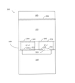
図2Aは、いくつかの実施形態によるピクセル100の図を示す。ピクセル100は、(光検出領域とも呼ばれる)光子吸収/キャリア発生領域102と、キャリア移動/捕獲領域106と、本明細書で「電荷キャリア貯蔵ビン」または単に「ビン」とも呼ばれる1つまたは複数の電荷キャリア貯蔵領域を有するキャリア貯蔵領域108と、電荷キャリア貯蔵ビンから信号を読み出すための読出回路構成110とを含む。
1)時間変動場から離れてテーパが付けられる空乏n型領域、
2)電場を横方向にn型領域へ遷移させるためのギャップを有するn型領域を取り囲むp型インプラント、および/または、
3)n型領域を埋設し寄生電子の再結合領域として機能する、p型表面インプラント。
図3は、光子吸収/キャリア発生領域102において発生する電荷キャリアが電荷キャリア貯蔵領域108における電荷貯蔵ビンに対し直接移送され得る、ピクセル200の一例を示す。そのようなピクセルは、「直接ビニングピクセル」と称される。図3に示されるように、ピクセル200はキャリア移動/捕獲領域106を含まない。キャリアをキャリア移動/捕獲領域106に捕獲するのではなく、電荷キャリアは光子吸収/キャリア発生領域102から電荷キャリア貯蔵領域108のビンへと直接移送され得る。電荷キャリアが移送されるビンは、電荷キャリアを生成する光子吸収/キャリア発生領域102における光子の到着の時間に基づく。直接ビニングピクセルのエリアは、キャリア移動/捕獲領域106の省略のため少なくとも部分的に減少されてよい。有利には、いくつかの実施形態では、直接ビニングピクセルは半導体チップのより小さいエリアを占めてよく、その半導体チップは、数千、もしくは数百万のピクセル、またはそれを超えるピクセルなど、多くのピクセルをチップ上に形成することができる。多数のピクセルをチップ上に提供することによって、多数の測定を並列に行うこと、または高い空間分解能にてイメージングを行うことが可能となり得る。これに加えてまたはこれに代えて、直接ビニングピクセルは、電力消費を低減してよい。ピクセルの各電極を充電および放電することは電力を消費し得るので、ピクセル200はより少ない電極の存在のため電力消費を低減することができ、すなわち、キャリア移動/捕獲領域106において電荷キャリアを捕獲するための電極を省略することが可能である。
図6に示されるように、ピクセル200は、電荷キャリア貯蔵領域108の電荷貯蔵ビンに貯蔵された電荷を読み出すことを可能にする読出回路構成110を含むことができる。ピクセル200は、読出回路構成110が読出増幅器を含むようなアクティブ・ピクセル、または読出回路構成110が読出増幅器を含まないパッシブ・ピクセルであり得る。任意の適切なタイプのアクティブ・ピクセルまたはパッシブ・ピクセル読出回路構成が使用されてよい。読出回路構成110が読出増幅器を含む場合、読出増幅器は、電荷貯蔵ビン(たとえば、ビン0,ビン1)に蓄積された電荷を入力として取り込むことができ、電荷貯蔵ビン内の電荷を表す電圧を出力として生成することができる。
任意の適切な数の時間ビンが使用されてよい。図3には、2つのビンを有するピクセルの例が示されている。しかしながら、任意の適切な数のビンを有するピクセルが、所望の時間分解能および他の因子に基づいて生成されてもよい。ビンの数の増加は、各ピクセルによって占められるエリアを増大させる可能性があり、ピクセルの全体数を減らすことによって、またはより小さい特徴サイズを有する作製プロセスを使用することによって達成され得る。少数のビンを使用することにより、チップに取り付けられるピクセルの数の増加を可能にすることができる。いくつかの実施形態では、特定の期間内に到着する光子の数を決定するために、単一のビンが使用され得る。
電荷貯蔵ビンを半導体領域内のポテンシャル井戸(ウェル)として実装するいくつかの手法がある。いくつかの実施形態では、ポテンシャル井戸は、部分的に電極203または205内にあってよい。電荷を井戸の中および井戸の外に移動するための2つのタイプの移送がある。蓄積の移送は電荷を井戸へと移動させる。読出部の移送は電荷を井戸の外に移動させる。
・井戸は、少なくとも100個の電子の蓄積された電荷を30℃にて10ms間に貯蔵するのに充分な深さであってよい。
・電極203または205は、領域102を井戸に対して電荷結合する。
・井戸は、少なくとも部分的に電極203または205内にあってよい。
・蓄積の移送中、井戸は領域102の完全な空乏電圧よりも高い電位にあってよい。
・井戸の完全な空乏電圧は、読出の移送中の浮遊拡散部リセット・レベルよりも低い電位にあってよい。
・井戸の電位は、蓄積の移送と読出の移送との両方の要求に適うように、動的に変調されてよい。
図10は、工程2802の除去期間中の電位を示し、また図5Aに対応する。左下のプロットは、図8のy次元に沿った電位を示す。光子吸収/キャリア発生領域102は、y=0に中心が置かれる。左下および左上のプロットに見られるように、y=0に関して左方への除去領域の電極が高くなるとき、電位はy=0の左方の除去領域に向かって降下する。したがって、キャリアは光子吸収/キャリア発生領域102から除去領域105に対して移送される。右下のプロットは、ドーピング濃度を示す。
縦方向除去
本発明者らは、半導体基板内の深くにおける電荷キャリアの光生成から問題が生じることを認識し理解している。基板内の深くにかなりの電位勾配がない場合があるので、この領域において生成されたキャリアは遅い移動であってよく、予測可能な経路を取らなくてよい。いくつかの場合では、深部で生成されたキャリアは、最終的に表面に移動してよく、領域102に閉じ込められてよい。そのようなキャリアは電流測定期間中に到着した光子に対応しないので、そのキャリアを領域102に収集することは望ましくなく、したがって、除去される必要があるノイズである。本発明者らは、直接ビニングピクセルまたは別のタイプのピクセルに用いられ得る、深部生成キャリアを除去する構造および技法を開発した。そのような構造および技法を論じる前に、深部生成キャリアの発生および移動が論じられる。
1)熱
2)ドリフト
3)拡散
から移動を受ける。
1)1つの技法は、埋設ドレインである。図19は、N型の埋設層(深部ドレイン)が高い電位(たとえば3ボルト)でバイアスがかけられている一例を示す。深部の光電子は、N型の埋設層へと引き込まれ、コンタクトにて排出される。
図21は、集積回路が作製され得る材料の例を示す。ピクセルは半導体領域に形成されてよく、いくつかの実施形態では半導体領域はシリコンであってよい。酸化シリコン領域などの絶縁領域は、集積回路のエリアを互いに絶縁してよい。電極(たとえば電極206,203および213)は、ポリシリコンまたは別の導体から形成されてよい。絶縁スペーサは電極の側に配置されてよい。たとえば、絶縁領域は窒化シリコンから形成されてよい。アルミニウムなどの金属が電極に対して電気的に接触するように電極上に配置されてよい。しかしながら、本明細書に説明されるデバイスは特定の材料に関して限定されないので、他の材料が用いられてよい。
例示的な集積回路の実現および集積光検出器の形成方法
いくつかの実施形態では、チップ1300は、標準的なCMOS(相補型金属酸化膜半導体)プロセスを使用してシリコン基板に形成され得る。しかしながら、本明細書に説明されている技法はこれに関して限定されず、任意の適切な基板または製造プロセスが使用されてよい。図28~図32は、光検出器を形成する例示的な処理と4つの異なるピクセル設計d0~d3とを示す。図28は、半導体領域における拡散部およびNウェル領域、ならびに上に位置するポリ電極層とともにレベル0を示す。図29はレベル1を示し、図30はレベル2を示し、図31はレベル3を示し、図32はレベル4を示す。
図33は、いくつかの実施形態によるチップ・アーキテクチャの図を示す。図33に示されるように、集積回路またはチップ1300は、複数のピクセル100を含むピクセル・アレイ1302と、タイミング回路1306を含む制御回路1304と、電圧/電流バイアス発生回路1305と、インターフェース1308とを含むことができる。
1)オンチップのデジタル制御されるピクセル・バイアス発生器(DAC)
2)シングルエンドのピクセル出力電圧信号を差動信号に変換し利得を信号に適用する、オンチップのデジタル・プログラマブル利得増幅器
3)出力レートで電力損失をスケーリングすることを可能にする、デジタル制御される増幅バイアス発生器(amplifier bias generators)。
本発明の様々な態様は、単独で、組み合わせて、または上記に説明された実施形態において特に議論されていない様々な構成で使用されてよく、したがって、その用途において、上記の説明に記載されまたは図面に示されている構成要素の詳細および構成に限定されない。たとえば、一実施形態において説明された態様が、他の実施形態において説明された態様と任意の様式で組み合わされてよい。
Claims (37)
- 入射光子を受け取るように構成された光検出領域であって、前記入射光子に応答して複数の電荷キャリアを生成するように構成された光検出領域と、
少なくとも1つの電荷キャリア貯蔵領域と、
前記複数の電荷キャリアのうちの電荷キャリアを、前記電荷キャリアが生成された時間に基づいて、前記少なくとも1つの電荷キャリア貯蔵領域内へ直接方向付けするべく、選択的に方向付けするように、また複数の励起光パルスに応答して生成された電荷キャリアを前記少なくとも1つの電荷キャリア貯蔵領域に集約するように構成された電荷キャリア分離構造と、を備える集積回路。 - 直接ビニングピクセルを備える集積回路であって、前記直接ビニングピクセルは、
入射光子を受け取るように構成された光検出領域であって、前記入射光子に応答して複数の電荷キャリアを生成するように構成された光検出領域と、
少なくとも1つの電荷キャリア貯蔵領域と、
前記複数の電荷キャリアのうちの電荷キャリアを、前記電荷キャリアが生成された時間に基づいて、前記少なくとも1つの電荷キャリア貯蔵領域内へ選択的に方向付けするように、また複数の励起光パルスに応答して生成された電荷キャリアを前記少なくとも1つの電荷キャリア貯蔵領域に集約するように構成された電荷キャリア分離構造と、を備える、集積回路。 - 複数のピクセルを備える集積回路であって、前記複数のピクセルのうちの第1のピクセルは、
入射光子を受け取るように構成された光検出領域であって、前記入射光子に応答して複数の電荷キャリアを生成するように構成された光検出領域と、
複数の電荷キャリア貯蔵領域と、
前記複数の電荷キャリアのうちの電荷キャリアを、前記電荷キャリアが生成された時間に基づいて、前記複数の電荷キャリア貯蔵領域のそれぞれの電荷キャリア貯蔵領域内へ直接方向付けするべく、選択的に方向付けするように、また複数の励起光パルスに応答して生成された電荷キャリアを前記複数の電荷キャリア貯蔵領域に集約するように構成された電荷キャリア分離構造と、を備える直接ビニングピクセルである集積回路。 - 前記電荷キャリア分離構造は、前記光検出領域と前記少なくとも1つの電荷キャリア貯蔵領域のうちの第1の電荷キャリア貯蔵領域との間の境界に少なくとも1つの電極を備える、請求項1~3のいずれか一項に記載の集積回路。
- 前記電荷キャリア分離構造は、前記光検出領域と前記第1の電荷キャリア貯蔵領域との間の前記境界に単一の電極を備える、請求項4に記載の集積回路。
- 電荷キャリア捕獲領域が前記直接ビニングピクセルに存在しないか、電荷キャリア捕獲領域が前記光検出領域と電荷キャリア貯蔵領域との間に存在しないか、またはその両方である、請求項2または3に記載の集積回路。
- 前記光検出領域と前記少なくとも1つの電荷キャリア貯蔵領域との間において前記キャリアを捕獲することなく、電荷キャリアが前記少なくとも1つの電荷キャリア貯蔵領域に対し移送される、請求項1~6のいずれか一項に記載の集積回路。
- 電荷キャリア除去領域が、除去期間中に前記光検出領域において生成された電荷キャリアを廃棄する、請求項1~7のいずれか一項に記載の集積回路。
- 廃棄された前記電荷キャリアは、キャリアが前記光検出領域から電荷キャリア貯蔵領域に向かって方向付けされる方向とは異なる方向において前記光検出領域から取り除かれる、請求項8に記載の集積回路。
- 電荷キャリア除去領域が、前記光検出領域と前記電荷キャリア除去領域との間の境界における電極の電圧を変化させることによって、除去期間中に前記光検出領域において生成された電荷キャリアを廃棄する、請求項8に記載の集積回路。
- 単一光子が、前記少なくとも1つの電荷キャリア貯蔵領域に対し移送され、前記少なくとも1つの電荷キャリア貯蔵領域に集約される、請求項1~10のいずれか一項に記載の集積回路。
- 半導体基板の表面の下において1マイクロメートルよりも深い位置にある電荷キャリアは除去される、請求項1~11のいずれか一項に記載の集積回路。
- 前記半導体基板の表面の下において1マイクロメートルよりも深い位置にある電荷キャリアは、前記光検出領域のフォトダイオードの下のインプラントによって少なくとも部分的に除去される、請求項12に記載の集積回路。
- 前記インプラントは深部遮蔽体または深部ドレインを提供する、請求項13に記載の集積回路。
- 前記インプラントはN型またはP+型である、請求項14に記載の集積回路。
- 前記半導体基板の表面の下において1マイクロメートルよりも深い位置にある電荷キャリアは、前記半導体基板の前記表面の下のドリフトの場によって除去される、請求項12または13に記載の集積回路。
- 前記光検出領域は、2マイクロメートル未満の深さであるエピタキシャル領域に形成されている、請求項1~3のいずれか一項に記載の集積回路。
- 前記光検出領域は、フォトダイオードを含むエピタキシャル領域である、請求項1~17のいずれか一項に記載の集積回路。
- 前記フォトダイオードにおける電荷キャリアは除去期間中に除去領域に対して移送され、次いで第1の電荷キャリア貯蔵領域に対する第1の電位障壁が低下され、次いで第2の電荷キャリア貯蔵領域に対する第2の電位障壁が低下される、請求項13または18に記載の集積回路。
- 前記第1の電位障壁は第1の電極によって制御され、前記第2の電位障壁は第2の電極によって制御される、請求項19に記載の集積回路。
- 前記少なくとも1つの電荷キャリア貯蔵領域は、複数の電荷キャリア貯蔵領域を含む、請求項1~20のいずれか一項に記載の集積回路。
- (A)直接ビニングピクセルの光検出領域において入射光子を受け取る工程と、
(B)前記入射光子に応答して生成された複数の電荷キャリアのうちの電荷キャリアを、前記電荷キャリアが生成された時間に基づいて、前記光検出領域から直接、前記直接ビニングピクセルの少なくとも1つの電荷キャリア貯蔵領域内へ選択的に方向付けし、複数の励起光パルスに応答して生成された電荷キャリアを前記少なくとも1つの電荷キャリア貯蔵領域に集約する工程と、を備える光検出方法。 - 電荷キャリア捕獲領域が前記直接ビニングピクセルに存在しないか、電荷キャリア捕獲領域が前記光検出領域と電荷キャリア貯蔵領域との間に存在しないか、またはその両方である、請求項22に記載の光検出方法。
- 前記光検出領域と前記少なくとも1つの電荷キャリア貯蔵領域との間において前記キャリアを捕獲することなく、電荷キャリアが前記少なくとも1つの電荷キャリア貯蔵領域に対し移送される、請求項22または23に記載の光検出方法。
- 電荷キャリア除去領域が、除去期間中に前記光検出領域において生成された電荷キャリアを廃棄する、請求項22~24のいずれか一項に記載の光検出方法。
- 廃棄された前記電荷キャリアは、キャリアが前記光検出領域から電荷キャリア貯蔵領域に向かって方向付けされる方向とは異なる方向において前記光検出領域から取り除かれる、請求項25に記載の光検出方法。
- 電荷キャリア除去領域が、前記光検出領域と前記電荷キャリア除去領域との間の境界における電極の電圧を変化させることによって、除去期間中に前記光検出領域において生成された電荷キャリアを廃棄する、請求項25に記載の光検出方法。
- 単一光子が、前記少なくとも1つの電荷キャリア貯蔵領域に対し移送され、前記少なくとも1つの電荷キャリア貯蔵領域に集約される、請求項22~27のいずれか一項に記載の光検出方法。
- 半導体基板の表面の下において1マイクロメートルよりも深い位置にある電荷キャリアは除去される、請求項22~28のいずれか一項に記載の光検出方法。
- 前記半導体基板の表面の下において1マイクロメートルよりも深い位置にある電荷キャリアは、前記光検出領域のフォトダイオードの下のインプラントによって少なくとも部分的に除去される、請求項29に記載の光検出方法。
- 前記インプラントは深部遮蔽体または深部ドレインを提供する、請求項30に記載の光検出方法。
- 前記インプラントはN型またはP+型である、請求項31に記載の光検出方法。
- 前記半導体基板の表面の下において1マイクロメートルよりも深い位置にある電荷キャリアは、前記半導体基板の前記表面の下のドリフトの場によって除去される、請求項29または30に記載の光検出方法。
- 前記光検出領域は、フォトダイオードを含むエピタキシャル領域である、請求項22~33のいずれか一項に記載の光検出方法。
- 前記フォトダイオードにおける電荷キャリアは除去期間中に除去領域に対して移送され、次いで第1の電荷キャリア貯蔵領域に対する第1の電位障壁が低下され、次いで第2の電荷キャリア貯蔵領域に対する第2の電位障壁が低下される、請求項30または34に記載の光検出方法。
- 前記第1の電位障壁は第1の電極によって制御され、前記第2の電位障壁は第2の電極によって制御される、請求項35に記載の光検出方法。
- 前記少なくとも1つの電荷キャリア貯蔵領域は、複数の電荷キャリア貯蔵領域を含む、請求項22~36のいずれか一項に記載の光検出方法。
Priority Applications (1)
| Application Number | Priority Date | Filing Date | Title |
|---|---|---|---|
| JP2022152536A JP7429744B2 (ja) | 2016-12-22 | 2022-09-26 | 直接ビニングピクセルを備える集積光検出器 |
Applications Claiming Priority (3)
| Application Number | Priority Date | Filing Date | Title |
|---|---|---|---|
| US201662438051P | 2016-12-22 | 2016-12-22 | |
| US62/438,051 | 2016-12-22 | ||
| PCT/US2017/068089 WO2018119347A1 (en) | 2016-12-22 | 2017-12-22 | Integrated photodetector with direct binning pixel |
Related Child Applications (1)
| Application Number | Title | Priority Date | Filing Date |
|---|---|---|---|
| JP2022152536A Division JP7429744B2 (ja) | 2016-12-22 | 2022-09-26 | 直接ビニングピクセルを備える集積光検出器 |
Publications (3)
| Publication Number | Publication Date |
|---|---|
| JP2020504507A JP2020504507A (ja) | 2020-02-06 |
| JP2020504507A5 JP2020504507A5 (ja) | 2021-02-04 |
| JP7149275B2 true JP7149275B2 (ja) | 2022-10-06 |
Family
ID=61018002
Family Applications (2)
| Application Number | Title | Priority Date | Filing Date |
|---|---|---|---|
| JP2019534096A Active JP7149275B2 (ja) | 2016-12-22 | 2017-12-22 | 直接ビニングピクセルを備える集積光検出器 |
| JP2022152536A Active JP7429744B2 (ja) | 2016-12-22 | 2022-09-26 | 直接ビニングピクセルを備える集積光検出器 |
Family Applications After (1)
| Application Number | Title | Priority Date | Filing Date |
|---|---|---|---|
| JP2022152536A Active JP7429744B2 (ja) | 2016-12-22 | 2022-09-26 | 直接ビニングピクセルを備える集積光検出器 |
Country Status (11)
| Country | Link |
|---|---|
| US (4) | US10845308B2 (ja) |
| EP (2) | EP3559995B1 (ja) |
| JP (2) | JP7149275B2 (ja) |
| KR (1) | KR102560427B1 (ja) |
| CN (2) | CN110168732B (ja) |
| AU (2) | AU2017382316B2 (ja) |
| BR (1) | BR112019012540A2 (ja) |
| CA (1) | CA3047826A1 (ja) |
| MX (2) | MX2019007530A (ja) |
| TW (2) | TWI836905B (ja) |
| WO (1) | WO2018119347A1 (ja) |
Families Citing this family (48)
| Publication number | Priority date | Publication date | Assignee | Title |
|---|---|---|---|---|
| KR102384909B1 (ko) | 2014-08-08 | 2022-04-11 | 퀀텀-에스아이 인코포레이티드 | 수신된 광자들의 시간 비닝을 위한 집적 디바이스 |
| US10418407B2 (en) | 2015-11-06 | 2019-09-17 | Artilux, Inc. | High-speed light sensing apparatus III |
| US10254389B2 (en) | 2015-11-06 | 2019-04-09 | Artilux Corporation | High-speed light sensing apparatus |
| US10886309B2 (en) | 2015-11-06 | 2021-01-05 | Artilux, Inc. | High-speed light sensing apparatus II |
| US10441174B2 (en) | 2016-02-17 | 2019-10-15 | Tesseract Health, Inc. | Sensor and device for lifetime imaging and detection applications |
| KR102560427B1 (ko) | 2016-12-22 | 2023-07-28 | 퀀텀-에스아이 인코포레이티드 | 직접 비닝 픽셀을 갖는 집적 광검출기 |
| CN111566261A (zh) | 2017-08-18 | 2020-08-21 | 诺迪勒思生物科技公司 | 选择结合试剂的方法 |
| US11105928B2 (en) | 2018-02-23 | 2021-08-31 | Artilux, Inc. | Light-sensing apparatus and light-sensing method thereof |
| TWI758599B (zh) | 2018-04-08 | 2022-03-21 | 美商光程研創股份有限公司 | 光偵測裝置 |
| WO2019222684A1 (en) * | 2018-05-18 | 2019-11-21 | The Charles Stark Draper Laboratory, Inc. | Convolved augmented range lidar nominal area |
| BR112020024790A2 (pt) | 2018-06-22 | 2021-03-02 | Quantum-Si Incorporated | fotodetector integrado com região de armazenamento de carga de tempo de detecção variado |
| WO2020022313A1 (ja) * | 2018-07-25 | 2020-01-30 | 株式会社デンソー | 光検出素子およびライダー装置 |
| JP7056439B2 (ja) * | 2018-07-25 | 2022-04-19 | 株式会社デンソー | 光検出素子およびライダー装置 |
| JP7070199B2 (ja) * | 2018-07-25 | 2022-05-18 | 株式会社デンソー | 光検出素子およびライダー装置 |
| US11018168B2 (en) * | 2018-09-20 | 2021-05-25 | Taiwan Semiconductor Manufacturing Co., Ltd. | Image sensor with improved timing resolution and photon detection probability |
| CA3117889A1 (en) | 2018-11-15 | 2020-05-22 | Quantum-Si Incorporated | Methods and compositions for protein sequencing |
| WO2020106889A1 (en) | 2018-11-20 | 2020-05-28 | Nautilus Biotechnology, Inc. | Design and selection of affinity reagents |
| CN111385495B (zh) * | 2018-12-29 | 2022-02-11 | 天津大学青岛海洋技术研究院 | 一种用于补偿tof传感器中电荷转移不完全的方法 |
| WO2020186252A1 (en) | 2019-03-14 | 2020-09-17 | Insilixa, Inc. | Methods and systems for time-gated fluorescent-based detection |
| JP2022525322A (ja) * | 2019-03-14 | 2022-05-12 | インシリクサ, インコーポレイテッド | 時間ゲート蛍光ベースの検出のための方法およびシステム |
| EP3948344A4 (en) * | 2019-05-01 | 2022-12-21 | Sense Photonics, Inc. | EVENT DRIVEN SHARED MEMORY PIXEL |
| KR20220025853A (ko) | 2019-06-28 | 2022-03-03 | 퀀텀-에스아이 인코포레이티드 | 광학적 및 전기적 2차 경로 제거 |
| EP4022681B1 (en) | 2019-08-28 | 2024-05-22 | Artilux, Inc. | Photo-detecting apparatus with low dark current |
| CN114930028A (zh) | 2019-10-29 | 2022-08-19 | 宽腾矽公司 | 流体的蠕动泵送以及相关联的方法、系统和装置 |
| CA3159371A1 (en) * | 2019-10-31 | 2021-05-06 | Quantum-Si Incorporated | Pixel with enhanced drain |
| KR102718982B1 (ko) * | 2019-12-05 | 2024-10-18 | 삼성전자주식회사 | 이미지 센서 |
| TW202143465A (zh) | 2020-01-14 | 2021-11-16 | 美商寬騰矽公司 | 用於壽命特性分析之整合感應器 |
| AU2021208557A1 (en) | 2020-01-14 | 2022-09-01 | Quantum-Si Incorporated | Sensor for lifetime plus spectral characterization |
| JP2023515682A (ja) | 2020-03-02 | 2023-04-13 | クアンタム-エスアイ インコーポレイテッド | 多次元信号解析用集積センサ |
| WO2021207400A2 (en) | 2020-04-08 | 2021-10-14 | Quantum-Si Incorporated | Integrated sensor with reduced skew |
| CN116134046A (zh) | 2020-05-20 | 2023-05-16 | 宽腾矽公司 | 用于蛋白质测序的方法及组合物 |
| US20220294998A1 (en) * | 2020-06-18 | 2022-09-15 | Facebook Technologies, Llc | Multimode detector for different time-of-flight based depth sensing modalities |
| IL302221A (en) | 2020-10-22 | 2023-06-01 | Quantum Si Inc | Integrated circuit with sequentially-coupled charge storage and associated techniques |
| US20220190012A1 (en) * | 2020-12-11 | 2022-06-16 | Quantum-Si Incorporated | Integrated circuit with improved charge transfer efficiency and associated techniques |
| EP4281775A1 (en) | 2021-01-21 | 2023-11-29 | Nautilus Subsidiary, Inc. | Systems and methods for biomolecule preparation |
| AU2022232933A1 (en) | 2021-03-11 | 2023-09-07 | Nautilus Subsidiary, Inc. | Systems and methods for biomolecule retention |
| CA3227872A1 (en) | 2021-09-09 | 2023-03-16 | James Henry JOLY | Characterization and localization of protein modifications |
| US20230090454A1 (en) | 2021-09-22 | 2023-03-23 | Nautilus Biotechnology, Inc. | Methods and systems for determining polypeptide interactions |
| WO2023081728A1 (en) | 2021-11-03 | 2023-05-11 | Nautilus Biotechnology, Inc. | Systems and methods for surface structuring |
| US20230262351A1 (en) * | 2022-02-15 | 2023-08-17 | Novatek Microelectronics Corp. | Image sensor |
| US12092578B2 (en) | 2022-03-29 | 2024-09-17 | Nautilus Subsidiary, Inc. | Integrated arrays for single-analyte processes |
| WO2023250364A1 (en) | 2022-06-21 | 2023-12-28 | Nautilus Subsidiary, Inc. | Method for detecting analytes at sites of optically non-resolvable distances |
| US12159887B2 (en) | 2022-08-19 | 2024-12-03 | Quantum-Si Incorporated | Backside illuminated structures with parallel charge transfer |
| WO2024073599A1 (en) | 2022-09-29 | 2024-04-04 | Nautilus Subsidiary, Inc. | Preparation of array surfaces for single-analyte processes |
| US20240192202A1 (en) | 2022-12-09 | 2024-06-13 | Nautilus Subsidiary, Inc. | Fluidic media for single-analtye arrays |
| US20240201182A1 (en) | 2022-12-15 | 2024-06-20 | Nautilus Subsidiary, Inc. | Inhibition of photon phenomena on single molecule arrays |
| US20240344116A1 (en) | 2023-03-24 | 2024-10-17 | Nautilus Subsidiary, Inc. | Transfer of nanoparticles to array surfaces |
| US20240394902A1 (en) | 2023-05-24 | 2024-11-28 | Nautilus Subsidiary, Inc. | Systems and methods for machine vision |
Citations (2)
| Publication number | Priority date | Publication date | Assignee | Title |
|---|---|---|---|---|
| JP2002170945A (ja) | 2000-11-30 | 2002-06-14 | Nec Corp | 固体撮像装置 |
| WO2007119626A1 (ja) | 2006-03-31 | 2007-10-25 | National University Corporation Shizuoka University | 半導体測距素子及び固体撮像装置 |
Family Cites Families (204)
| Publication number | Priority date | Publication date | Assignee | Title |
|---|---|---|---|---|
| US3890500A (en) * | 1974-02-11 | 1975-06-17 | Gen Electric | Apparatus for sensing radiation and providing electrical readout |
| US5198543A (en) | 1989-03-24 | 1993-03-30 | Consejo Superior Investigaciones Cientificas | PHI29 DNA polymerase |
| US5302509A (en) | 1989-08-14 | 1994-04-12 | Beckman Instruments, Inc. | Method for sequencing polynucleotides |
| EP0450060A1 (en) | 1989-10-26 | 1991-10-09 | Sri International | Dna sequencing |
| US5355165A (en) | 1992-08-06 | 1994-10-11 | Princeton Scientific Instruments, Inc. | Very high frame rate CCD imager |
| CA2155186A1 (en) | 1993-02-01 | 1994-08-18 | Kevin M. Ulmer | Methods and apparatus for dna sequencing |
| US5471515A (en) | 1994-01-28 | 1995-11-28 | California Institute Of Technology | Active pixel sensor with intra-pixel charge transfer |
| MXPA96005828A (es) | 1994-05-27 | 2005-07-15 | Novartis Ag Tambien Denominada | Proceso para detectar luminescencia excitada evanescentemente. |
| US5912155A (en) | 1994-09-30 | 1999-06-15 | Life Technologies, Inc. | Cloned DNA polymerases from Thermotoga neapolitana |
| US5814565A (en) | 1995-02-23 | 1998-09-29 | University Of Utah Research Foundation | Integrated optic waveguide immunosensor |
| US6261797B1 (en) | 1996-01-29 | 2001-07-17 | Stratagene | Primer-mediated polynucleotide synthesis and manipulation techniques |
| US6198869B1 (en) | 1996-11-18 | 2001-03-06 | Novartis Ag | Measuring device and its use |
| ATE273381T1 (de) | 1997-02-12 | 2004-08-15 | Eugene Y Chan | Verfahren zur analyse von polymeren |
| IT1290553B1 (it) * | 1997-02-27 | 1998-12-10 | Ist Nazionale Fisica Nucleare | Rivelatore dell'energia e della posizione di incidenza di radiazioni elettromagnetiche o di particelle ionizzanti a deriva controllata |
| JP3435416B2 (ja) | 1997-03-12 | 2003-08-11 | ピーイー コーポレイション(エヌワイ) | 改善された標識ヌクレオチド取込み特性を有するdnaポリメラーゼ |
| US6327410B1 (en) | 1997-03-14 | 2001-12-04 | The Trustees Of Tufts College | Target analyte sensors utilizing Microspheres |
| US6825921B1 (en) | 1999-11-10 | 2004-11-30 | Molecular Devices Corporation | Multi-mode light detection system |
| DE19748211A1 (de) | 1997-10-31 | 1999-05-06 | Zeiss Carl Fa | Optisches Array-System und Reader für Mikrotiterplatten |
| EP0921196A1 (en) | 1997-12-02 | 1999-06-09 | Roche Diagnostics GmbH | Modified DNA-polymerase from carboxydothermus hydrogenoformans and its use for coupled reverse transcription and polymerase chain reaction |
| DE19810879A1 (de) | 1998-03-13 | 1999-09-16 | Roche Diagnostics Gmbh | Polymerasenchimären |
| AU3199699A (en) | 1998-03-23 | 1999-10-18 | Invitrogen Corporation | Modified nucleotides and methods useful for nucleic acid sequencing |
| US7875440B2 (en) | 1998-05-01 | 2011-01-25 | Arizona Board Of Regents | Method of determining the nucleotide sequence of oligonucleotides and DNA molecules |
| GB9810350D0 (en) | 1998-05-14 | 1998-07-15 | Ciba Geigy Ag | Organic compounds |
| US6787308B2 (en) | 1998-07-30 | 2004-09-07 | Solexa Ltd. | Arrayed biomolecules and their use in sequencing |
| US6716394B2 (en) | 1998-08-11 | 2004-04-06 | Caliper Technologies Corp. | DNA sequencing using multiple fluorescent labels being distinguishable by their decay times |
| US6210896B1 (en) | 1998-08-13 | 2001-04-03 | Us Genomics | Molecular motors |
| US6280939B1 (en) | 1998-09-01 | 2001-08-28 | Veeco Instruments, Inc. | Method and apparatus for DNA sequencing using a local sensitive force detector |
| JP4326050B2 (ja) | 1998-09-22 | 2009-09-02 | ハイスペック合資会社 | 高速撮像素子 |
| US6232075B1 (en) | 1998-12-14 | 2001-05-15 | Li-Cor, Inc. | Heterogeneous assay for pyrophosphate detection |
| US6445491B2 (en) | 1999-01-29 | 2002-09-03 | Irma America, Inc. | Method and apparatus for optical sectioning and imaging using time-gated parametric image amplification |
| JP2002537858A (ja) | 1999-03-10 | 2002-11-12 | エーエスエム サイエンティフィック, インコーポレイテッド | 核酸の配列を直接決定するための方法 |
| EP1681356B1 (en) | 1999-05-19 | 2011-10-19 | Cornell Research Foundation, Inc. | Method for sequencing nucleic acid molecules |
| US7056661B2 (en) | 1999-05-19 | 2006-06-06 | Cornell Research Foundation, Inc. | Method for sequencing nucleic acid molecules |
| US6137117A (en) | 1999-06-21 | 2000-10-24 | The United States Of America As Represented By The Secretary Of The Navy | Integrating multi-waveguide sensor |
| CN2433618Y (zh) | 1999-10-29 | 2001-06-06 | 中国科学院上海原子核研究所 | 基因芯片检测装置 |
| US6399335B1 (en) | 1999-11-16 | 2002-06-04 | Advanced Research And Technology Institute, Inc. | γ-phosphoester nucleoside triphosphates |
| JP4433347B2 (ja) | 2000-01-17 | 2010-03-17 | 富士フイルム株式会社 | 蛍光撮像装置 |
| US20020090650A1 (en) * | 2000-04-06 | 2002-07-11 | Quantum Dot Corporation | Two-dimensional spectral imaging system |
| JP2003532123A (ja) | 2000-04-28 | 2003-10-28 | エッジライト バイオサイエンシズ インコーポレイテッド | マイクロアレーエバネッセント波蛍光検出装置 |
| US6917726B2 (en) | 2001-09-27 | 2005-07-12 | Cornell Research Foundation, Inc. | Zero-mode clad waveguides for performing spectroscopy with confined effective observation volumes |
| US6936702B2 (en) | 2000-06-07 | 2005-08-30 | Li-Cor, Inc. | Charge-switch nucleotides |
| US6975898B2 (en) | 2000-06-19 | 2005-12-13 | University Of Washington | Medical imaging, diagnosis, and therapy using a scanning single optical fiber system |
| WO2002001194A1 (en) | 2000-06-25 | 2002-01-03 | Affymetrix, Inc. | Optically active substrates |
| FR2813121A1 (fr) | 2000-08-21 | 2002-02-22 | Claude Weisbuch | Dispositif perfectionne de support d'elements chromophores |
| EP1320596A4 (en) | 2000-08-30 | 2005-01-12 | Univ Rochester | REVERSE TRANSCRIPTION REACTION METHOD USING REVERSE TRANSCRIPTASE CODED BY RETROTRANSPOSON NON-LTR |
| WO2002023167A1 (en) | 2000-09-11 | 2002-03-21 | The Government Of The United States Of America, As Represented By The Secretary Of The Navy | Fluidics system |
| EP1207387A1 (en) | 2000-11-20 | 2002-05-22 | Institut Curie | Multi-photon imaging installation. |
| US7668697B2 (en) | 2006-02-06 | 2010-02-23 | Andrei Volkov | Method for analyzing dynamic detectable events at the single molecule level |
| US7033762B2 (en) | 2001-08-29 | 2006-04-25 | Amersham Biosciences Corp | Single nucleotide amplification and detection by polymerase |
| CA2460546A1 (en) | 2001-09-14 | 2003-03-27 | Invitrogen Corporation | Dna polymerases and mutants thereof |
| US7057026B2 (en) | 2001-12-04 | 2006-06-06 | Solexa Limited | Labelled nucleotides |
| GB2382648B (en) * | 2001-12-11 | 2003-11-12 | Amersham Pharm Biotech Uk Ltd | System and method for time correlated multi-photon counting measurements |
| CN1138862C (zh) | 2002-01-28 | 2004-02-18 | 国前 | 一种核酸分析用收集装置及其应用方法 |
| US7179654B2 (en) | 2002-03-18 | 2007-02-20 | Agilent Technologies, Inc. | Biochemical assay with programmable array detection |
| US6924887B2 (en) | 2002-03-27 | 2005-08-02 | Sarnoff Corporation | Method and apparatus for generating charge from a light pulse |
| US8238993B2 (en) | 2002-04-04 | 2012-08-07 | Veralight, Inc. | Determination of a measure of a glycation end-product or disease state using tissue fluorescence lifetime |
| US20040144927A1 (en) | 2003-01-28 | 2004-07-29 | Auner Gregory W. | Microsystems arrays for digital radiation imaging and signal processing and method for making microsystem arrays |
| US7595883B1 (en) | 2002-09-16 | 2009-09-29 | The Board Of Trustees Of The Leland Stanford Junior University | Biological analysis arrangement and approach therefor |
| US20040106163A1 (en) | 2002-11-12 | 2004-06-03 | Workman Jerome James | Non-invasive measurement of analytes |
| AU2003294365A1 (en) | 2002-11-19 | 2004-06-15 | Safetzone Technologies Corporation | Guest communication system and method |
| EP1592779A4 (en) | 2003-02-05 | 2007-12-12 | Ge Healthcare Bio Sciences | PHOSPHATE-ENDMARKED NUCLEOTIDES WITH NEW LINKERS |
| WO2004092331A2 (en) | 2003-04-08 | 2004-10-28 | Li-Cor, Inc. | Composition and method for nucleic acid sequencing |
| FR2857158B1 (fr) * | 2003-07-01 | 2006-04-28 | St Microelectronics Sa | Procede de commande d'un photocopieur de type mos |
| US7078670B2 (en) | 2003-09-15 | 2006-07-18 | Imagerlabs, Inc. | Low noise charge gain circuit and CCD using same |
| WO2005073407A1 (en) | 2003-10-07 | 2005-08-11 | Ut-Battelle, Llc | Advanced integrated circuit biochip |
| DE10348949A1 (de) | 2003-10-18 | 2005-05-19 | Bayer Healthcare Ag | Direkte Beobachtung molekularer Veränderungen ind biologischen Testsystemen mittels Messungen der Fluoreszenz-Lebensdauer |
| US20070042500A1 (en) | 2003-10-18 | 2007-02-22 | Bayer Healthcare Ag | Direct observation of molecular modifications in biological test systems by measuring flourescence lifetime |
| US20070281288A1 (en) | 2004-01-27 | 2007-12-06 | Shimshon Belkin | Method and System for Detecting Analytes |
| WO2005080605A2 (en) | 2004-02-19 | 2005-09-01 | Helicos Biosciences Corporation | Methods and kits for analyzing polynucleotide sequences |
| EP1583150A1 (en) * | 2004-03-31 | 2005-10-05 | CSEM Centre Suisse d'Electronique et de Microtechnique SA | Image sensor with large-area, high-sensitivity and high-speed pixels |
| US7462452B2 (en) | 2004-04-30 | 2008-12-09 | Pacific Biosciences Of California, Inc. | Field-switch sequencing |
| US20060019265A1 (en) | 2004-04-30 | 2006-01-26 | Kimberly-Clark Worldwide, Inc. | Transmission-based luminescent detection systems |
| EP1622200A1 (en) | 2004-07-26 | 2006-02-01 | CSEM Centre Suisse d'Electronique et de Microtechnique SA | Solid-state photodetector pixel and photodetecting method |
| US7170050B2 (en) | 2004-09-17 | 2007-01-30 | Pacific Biosciences Of California, Inc. | Apparatus and methods for optical analysis of molecules |
| US7345764B2 (en) | 2005-02-07 | 2008-03-18 | Vladimir Bulovic | Apparatus and method for a slim format spectrometer |
| US20060223067A1 (en) | 2005-03-31 | 2006-10-05 | Paolo Vatta | Mutant DNA polymerases and methods of use |
| US7365299B2 (en) | 2005-05-09 | 2008-04-29 | Sensors Unlimited, Inc. | Method and apparatus for providing flexible photodetector binning |
| US7738086B2 (en) | 2005-05-09 | 2010-06-15 | The Trustees Of Columbia University In The City Of New York | Active CMOS biosensor chip for fluorescent-based detection |
| WO2007002890A2 (en) | 2005-06-28 | 2007-01-04 | Agencourt Personal Genomics Corporation | Methods of producing and sequencing modified polynucleotides |
| US8481697B2 (en) | 2005-07-01 | 2013-07-09 | Dako Denmark A/S | Nucleic acid base pairs |
| US7426322B2 (en) | 2005-07-20 | 2008-09-16 | Searete Llc. | Plasmon photocatalysis |
| US7405281B2 (en) | 2005-09-29 | 2008-07-29 | Pacific Biosciences Of California, Inc. | Fluorescent nucleotide analogs and uses therefor |
| US7501631B2 (en) * | 2005-10-07 | 2009-03-10 | Schick Technologies, Inc. | Shielding an imaging array from X-ray noise |
| WO2007070542A2 (en) | 2005-12-12 | 2007-06-21 | The Government Of The United States Of America As Represented By The Secretary Of The Deptartment Ofhealth And Human Services | Nanoprobes for detection or modification of molecules |
| EP1963536B1 (en) | 2005-12-22 | 2016-05-04 | Pacific Biosciences of California, Inc. | Polymerases for nucleotide analogue incorporation |
| EP1963530B1 (en) | 2005-12-22 | 2011-07-27 | Pacific Biosciences of California, Inc. | Active surface coupled polymerases |
| US7995202B2 (en) | 2006-02-13 | 2011-08-09 | Pacific Biosciences Of California, Inc. | Methods and systems for simultaneous real-time monitoring of optical signals from multiple sources |
| US7715001B2 (en) | 2006-02-13 | 2010-05-11 | Pacific Biosciences Of California, Inc. | Methods and systems for simultaneous real-time monitoring of optical signals from multiple sources |
| US8975216B2 (en) | 2006-03-30 | 2015-03-10 | Pacific Biosciences Of California | Articles having localized molecules disposed thereon and methods of producing same |
| US20080050747A1 (en) | 2006-03-30 | 2008-02-28 | Pacific Biosciences Of California, Inc. | Articles having localized molecules disposed thereon and methods of producing and using same |
| DE102006030541B4 (de) | 2006-06-23 | 2010-05-12 | Fraunhofer-Gesellschaft zur Förderung der angewandten Forschung e.V. | Optische Anordnung |
| US8207509B2 (en) | 2006-09-01 | 2012-06-26 | Pacific Biosciences Of California, Inc. | Substrates, systems and methods for analyzing materials |
| US8471230B2 (en) | 2006-09-01 | 2013-06-25 | Pacific Biosciences Of California, Inc. | Waveguide substrates and optical systems and methods of use thereof |
| WO2008028160A2 (en) | 2006-09-01 | 2008-03-06 | Pacific Biosciences Of California, Inc. | Substrates, systems and methods for analyzing materials |
| JP4710017B2 (ja) | 2006-10-20 | 2011-06-29 | 国立大学法人静岡大学 | Cmosイメージセンサ |
| US8343746B2 (en) | 2006-10-23 | 2013-01-01 | Pacific Biosciences Of California, Inc. | Polymerase enzymes and reagents for enhanced nucleic acid sequencing |
| FR2908888B1 (fr) | 2006-11-21 | 2012-08-03 | Centre Nat Rech Scient | Dispositif pour la detection exaltee de l'emission d'une particule cible |
| US8289427B2 (en) | 2006-11-30 | 2012-10-16 | National University Corporation Shizuoka University | Semiconductor range-finding element and solid-state imaging device |
| JP5270835B2 (ja) | 2006-12-29 | 2013-08-21 | パナソニック株式会社 | 光検出素子、空間情報の検出装置 |
| EP2132556B1 (en) | 2007-03-22 | 2011-05-11 | Universite De Strasbourg (Etablissement Public à Caractère Scientifique, Culturel et Professionel) | Device for sorting and concentrating electromagnetic energy and apparatus comprising at least one such device |
| US20080241866A1 (en) | 2007-03-30 | 2008-10-02 | Pacific Biosciences Of California, Inc. | Systems and methods for enhancing fluorescent signals |
| US7873085B2 (en) | 2007-10-23 | 2011-01-18 | Andrei Babushkin | Method and device for controlling optical output of laser diode |
| WO2009082706A1 (en) | 2007-12-21 | 2009-07-02 | The Trustees Of Columbia University In The City Of New York | Active cmos sensor array for electrochemical biomolecular detection |
| WO2009091847A2 (en) | 2008-01-14 | 2009-07-23 | Life Technologies Corporation | Compositions, methods and systems for single molecule sequencing |
| US8501922B2 (en) | 2008-02-07 | 2013-08-06 | Pacific Biosciences Of California, Inc. | CIS reactive oxygen quenchers integrated into linkers |
| EP2263087B1 (en) | 2008-03-13 | 2017-08-09 | Pacific Biosciences of California, Inc. | Labeled reactants and their uses |
| US7973146B2 (en) | 2008-03-26 | 2011-07-05 | Pacific Biosciences Of California, Inc. | Engineered fluorescent dye labeled nucleotide analogs for DNA sequencing |
| EP3170904B1 (en) | 2008-03-28 | 2017-08-16 | Pacific Biosciences Of California, Inc. | Compositions and methods for nucleic acid sequencing |
| EP2286217B1 (en) | 2008-03-31 | 2015-02-18 | Pacific Biosciences of California, Inc. | Single molecule loading methods and compositions |
| US8133672B2 (en) | 2008-03-31 | 2012-03-13 | Pacific Biosciences Of California, Inc. | Two slow-step polymerase enzyme systems and methods |
| US9127259B2 (en) | 2008-03-31 | 2015-09-08 | Pacific Biosciences Of California, Inc. | Enzymes resistant to photodamage |
| JP5283216B2 (ja) * | 2008-07-31 | 2013-09-04 | 国立大学法人静岡大学 | 高速電荷転送フォトダイオード、ロックインピクセル及び固体撮像装置 |
| WO2010025331A1 (en) | 2008-08-28 | 2010-03-04 | Mesa Imaging Ag | Demodulation pixel with daisy chain charge storage sites and method of operation therefor |
| US20100148221A1 (en) * | 2008-11-13 | 2010-06-17 | Zena Technologies, Inc. | Vertical photogate (vpg) pixel structure with nanowires |
| US8481264B2 (en) | 2008-09-19 | 2013-07-09 | Pacific Biosciences Of California, Inc. | Immobilized nucleic acid complexes for sequence analysis |
| US9156010B2 (en) | 2008-09-23 | 2015-10-13 | Bio-Rad Laboratories, Inc. | Droplet-based assay system |
| AU2009300369B2 (en) | 2008-09-30 | 2014-08-14 | Pacific Biosciences Of California, Inc. | Ultra-high multiplex analytical systems and methods |
| EP2182523B1 (en) | 2008-10-31 | 2013-01-09 | CSEM Centre Suisse d'Electronique et de Microtechnique SA -Recherche et Développement | Charge sampling device and method based on a MOS-transmission line |
| WO2010057185A1 (en) | 2008-11-17 | 2010-05-20 | Pacific Biosciences Of California, Inc. | Phospholink nucleotides for sequencing applications |
| CN102388321B (zh) | 2008-12-22 | 2014-10-22 | 皇家飞利浦电子股份有限公司 | 高动态范围光传感器 |
| WO2010074252A1 (ja) | 2008-12-25 | 2010-07-01 | 国立大学法人静岡大学 | 半導体素子及び固体撮像装置 |
| EP2391655B1 (en) | 2009-01-30 | 2017-10-11 | Oxford Nanopore Technologies Limited | Hybridization linkers |
| BRPI0924456A2 (pt) | 2009-03-12 | 2016-02-16 | Rsp Systems As | sonda óptica para medir sinais de luz, e, método para coletar sinais ópticos de uma amostra. |
| WO2010111686A2 (en) | 2009-03-27 | 2010-09-30 | Life Technologies Corp | Labeled enzyme compositions, methods & systems |
| WO2010117420A2 (en) | 2009-03-30 | 2010-10-14 | Pacific Biosciences Of California, Inc. | Fret-labeled compounds and uses therefor |
| JP5415805B2 (ja) | 2009-03-31 | 2014-02-12 | オリンパスメディカルシステムズ株式会社 | 診断支援装置 |
| CN102395874B (zh) | 2009-04-15 | 2014-10-15 | 皇家飞利浦电子股份有限公司 | 时间控制荧光检测装置 |
| JP4798254B2 (ja) * | 2009-05-13 | 2011-10-19 | 株式会社デンソー | 受光デバイス及びその制御方法 |
| EP2443427B1 (en) * | 2009-06-17 | 2014-04-02 | Ingeneron, Inc. | Method and apparatus for quantitative microimaging |
| US8501406B1 (en) | 2009-07-14 | 2013-08-06 | Pacific Biosciences Of California, Inc. | Selectively functionalized arrays |
| CN102548466A (zh) | 2009-07-28 | 2012-07-04 | 霍夫曼-拉罗奇有限公司 | 非侵入性体内光学成像方法 |
| DE102009037596B4 (de) * | 2009-08-14 | 2014-07-24 | Fraunhofer-Gesellschaft zur Förderung der angewandten Forschung e.V. | Pixelstruktur, System und Verfahren zur optischen Abstandsmessung sowie Steuerschaltung für die Pixelstruktur |
| KR101363532B1 (ko) * | 2009-10-05 | 2014-02-14 | 고쿠리츠 다이가꾸 호우진 시즈오까 다이가꾸 | 반도체 소자 및 고체 촬상 장치 |
| US8278728B2 (en) | 2009-10-17 | 2012-10-02 | Florida Institute Of Technology | Array of concentric CMOS photodiodes for detection and de-multiplexing of spatially modulated optical channels |
| US9579402B2 (en) | 2009-12-04 | 2017-02-28 | Biotium, Inc. | Heterocycle-substituted xanthene dyes |
| JP6017107B2 (ja) | 2009-12-28 | 2016-10-26 | ソニー株式会社 | イメージセンサ及びその製造方法、並びにセンサデバイス |
| WO2011090745A1 (en) | 2009-12-29 | 2011-07-28 | Life Technologies Corporation | Single molecule detection and sequencing using fluorescence lifetime imaging |
| EP2362207A1 (de) | 2010-01-28 | 2011-08-31 | F. Hoffmann-La Roche AG | Messsystem und Messverfahren insbesondere zur Blutzuckerbestimmung |
| CA2790393C (en) | 2010-02-19 | 2019-03-12 | Pacific Biosciences Of California, Inc. | Integrated analytical system and method |
| JP5881120B2 (ja) | 2010-02-19 | 2016-03-09 | グリシュア リミテッド | 血管内グルコースセンサ |
| US20130005047A1 (en) | 2010-03-25 | 2013-01-03 | Mocon, Inc. | Luminescence lifetime based analyte sensing instruments and calibration technique |
| WO2011150431A1 (en) | 2010-05-28 | 2011-12-01 | The Regents Of The University Of Colorado, A Body Corporate | Multi-photon tissue imaging |
| US8865078B2 (en) | 2010-06-11 | 2014-10-21 | Industrial Technology Research Institute | Apparatus for single-molecule detection |
| US8865077B2 (en) | 2010-06-11 | 2014-10-21 | Industrial Technology Research Institute | Apparatus for single-molecule detection |
| JP2012132741A (ja) | 2010-12-21 | 2012-07-12 | Fujifilm Corp | 時間分解蛍光測定装置、及び方法 |
| JP2012134827A (ja) * | 2010-12-22 | 2012-07-12 | Toshiba Corp | 放射線画像検出器 |
| US8946845B1 (en) * | 2011-02-02 | 2015-02-03 | Aptina Imaging Corporation | Stacked pixels for high resolution CMOS image sensors with BCMD charge detectors |
| TWI553887B (zh) * | 2011-02-21 | 2016-10-11 | 美國密西根州立大學 | 嵌入電子傳導激子阻隔層的有機光伏打電池 |
| WO2012117670A1 (ja) * | 2011-03-01 | 2012-09-07 | パナソニック株式会社 | 固体撮像装置 |
| EP2689028B1 (en) | 2011-03-23 | 2017-08-30 | Pacific Biosciences Of California, Inc. | Isolation of polymerase-nucleic acid complexes and loading onto substrates |
| WO2013040058A1 (en) | 2011-09-12 | 2013-03-21 | Jian Guo | Imaging fluorescence or luminescence lifetime |
| US20130090537A1 (en) | 2011-10-07 | 2013-04-11 | 2M Engineering Limited | Blood glucose sensor |
| AU2012328662B2 (en) | 2011-10-28 | 2015-12-17 | Illumina, Inc. | Microarray fabrication system and method |
| WO2013066959A1 (en) | 2011-10-31 | 2013-05-10 | The Trustees Of Columbia University In The City Of New York | Systems and methods for imaging using single photon avalanche diodes |
| US8804021B2 (en) * | 2011-11-03 | 2014-08-12 | Omnivision Technologies, Inc. | Method, apparatus and system for providing improved full well capacity in an image sensor pixel |
| US9606060B2 (en) | 2012-01-13 | 2017-03-28 | California Institute Of Technology | Filterless time-domain detection of one or more fluorophores |
| US8906660B2 (en) | 2012-02-01 | 2014-12-09 | Pacific Biosciences Of California, Inc. | Recombinant polymerases with increased phototolerance |
| EP2814953B1 (en) | 2012-02-15 | 2017-06-07 | Pacific Biosciences Of California, Inc. | Polymerase enzyme substrates with protein shield |
| DE102012206089B4 (de) * | 2012-03-15 | 2017-02-02 | Fraunhofer-Gesellschaft zur Förderung der angewandten Forschung e.V. | Halbleiterstruktur, verfahren zum betreiben derselben und herstellungsverfahren |
| US20130256822A1 (en) * | 2012-03-28 | 2013-10-03 | Omnivision Technologies, Inc. | Method and device with enhanced ion doping |
| CN102914525B (zh) | 2012-04-10 | 2016-06-01 | 广东工业大学 | 基于光学加法外差调制的新型荧光寿命显微成像装置及方法 |
| WO2013171197A1 (en) | 2012-05-15 | 2013-11-21 | Ait Austrian Institute Of Technology Gmbh | Compact plasmon-enhanced fluorescence biosensor |
| US9372308B1 (en) | 2012-06-17 | 2016-06-21 | Pacific Biosciences Of California, Inc. | Arrays of integrated analytical devices and methods for production |
| AU2013306373B2 (en) | 2012-08-20 | 2017-09-07 | Illumina, Inc. | Method and system for fluorescence lifetime based sequencing |
| JP6281771B2 (ja) * | 2012-10-30 | 2018-02-21 | パナソニックIpマネジメント株式会社 | 蛍光検出装置 |
| NL2011568A (en) | 2012-10-31 | 2014-05-06 | Asml Netherlands Bv | Sensor and lithographic apparatus. |
| EP2936222B1 (en) | 2012-12-18 | 2019-07-03 | Pacific Biosciences Of California, Inc. | An optical analytical device |
| KR102370239B1 (ko) * | 2012-12-28 | 2022-03-04 | 가부시키가이샤 한도오따이 에네루기 켄큐쇼 | 반도체 장치 |
| GB201302664D0 (en) | 2013-02-15 | 2013-04-03 | Cmosis Nv | A pixel structure |
| JP6363114B2 (ja) * | 2013-02-28 | 2018-07-25 | デピュイ・シンセス・プロダクツ・インコーポレイテッド | Cmosセンサによる声帯のビデオストロボスコピー |
| US9741754B2 (en) * | 2013-03-06 | 2017-08-22 | Apple Inc. | Charge transfer circuit with storage nodes in image sensors |
| KR102007277B1 (ko) * | 2013-03-11 | 2019-08-05 | 삼성전자주식회사 | 3차원 이미지 센서의 거리 픽셀 및 이를 포함하는 3차원 이미지 센서 |
| WO2015006345A2 (en) | 2013-07-09 | 2015-01-15 | Nd Industries, Inc. | Multi-row magnetic dial for the conveyance of workpieces and related method |
| US20150042954A1 (en) | 2013-08-08 | 2015-02-12 | University Of Rochester | System and Method for Fluorescence Lifetime Imaging Aided by Adaptive Optics |
| KR102399962B1 (ko) | 2013-11-17 | 2022-05-20 | 퀀텀-에스아이 인코포레이티드 | 분자들을 검사, 검출 및 분석하기 위한 광 시스템 및 어세이 칩 |
| JP2016001712A (ja) * | 2013-11-29 | 2016-01-07 | 株式会社半導体エネルギー研究所 | 半導体装置の作製方法 |
| US10104318B2 (en) * | 2013-12-04 | 2018-10-16 | Rambus Inc. | High dynamic-range image sensor |
| CN103728446B (zh) | 2013-12-11 | 2016-02-24 | 天津大学 | 光子计数型多通道时间分辨荧光免疫分析系统及计数方法 |
| US9736388B2 (en) | 2013-12-13 | 2017-08-15 | Bio-Rad Laboratories, Inc. | Non-destructive read operations with dynamically growing images |
| EP3099232B1 (en) | 2014-01-31 | 2021-08-18 | The General Hospital Corporation | System and method for photoluminescence detection |
| TWI665778B (zh) * | 2014-02-05 | 2019-07-11 | 日商半導體能源研究所股份有限公司 | 半導體裝置、模組及電子裝置 |
| US9765395B2 (en) | 2014-04-28 | 2017-09-19 | Nanomedical Diagnostics, Inc. | System and method for DNA sequencing and blood chemistry analysis |
| KR20150134543A (ko) * | 2014-05-22 | 2015-12-02 | 삼성전자주식회사 | 소자 제조용 기판 및 반도체 소자 |
| CN115844328A (zh) * | 2014-07-24 | 2023-03-28 | 大学健康网络 | 用于诊断目的的数据的收集和分析 |
| WO2016016761A1 (en) * | 2014-07-31 | 2016-02-04 | Semiconductor Energy Laboratory Co., Ltd. | Method of manufacturing semiconductor device |
| KR102384909B1 (ko) | 2014-08-08 | 2022-04-11 | 퀀텀-에스아이 인코포레이티드 | 수신된 광자들의 시간 비닝을 위한 집적 디바이스 |
| KR102738114B1 (ko) * | 2014-08-08 | 2024-12-06 | 퀀텀-에스아이 인코포레이티드 | 분자들을 프로빙, 검출 및 분석하기 위한 광학계 및 검정 칩 |
| CN106796176B (zh) * | 2014-08-08 | 2021-02-05 | 宽腾矽公司 | 用于对分子进行探测、检测和分析的带外部光源的集成装置 |
| US10174363B2 (en) | 2015-05-20 | 2019-01-08 | Quantum-Si Incorporated | Methods for nucleic acid sequencing |
| KR20170097748A (ko) * | 2014-12-19 | 2017-08-28 | 쥐-레이 스위츨란드 에스에이 | 모놀리식 cmos 통합된 픽셀 검출기와, 다양한 적용예를 포함하는 입자 검출 및 이미지화를 위한 시스템 및 방법 |
| US9871065B2 (en) | 2014-12-22 | 2018-01-16 | Google Inc. | RGBZ pixel unit cell with first and second Z transfer gates |
| US9666748B2 (en) | 2015-01-14 | 2017-05-30 | International Business Machines Corporation | Integrated on chip detector and zero waveguide module structure for use in DNA sequencing |
| JP6302146B1 (ja) | 2015-02-09 | 2018-03-28 | エスプロス フォトニックス アーゲー | Tof距離センサ |
| EP4220256A1 (en) | 2015-03-16 | 2023-08-02 | Pacific Biosciences of California, Inc. | Analytical system comprising integrated devices and systems for free-space optical coupling |
| MX2022001187A (es) | 2015-05-20 | 2023-01-04 | Quantum Si Inc | Método para determinar la secuencia de un ácido nucleico usando luminiscencia resuelta por tiempo. |
| US10976257B2 (en) | 2015-06-08 | 2021-04-13 | The Regents Of The University Of Michigan | Pixel circuit and method for optical sensing |
| CN105300949B (zh) | 2015-11-26 | 2019-06-11 | 浙江大学 | 一种荧光寿命测量方法及装置 |
| US10441174B2 (en) | 2016-02-17 | 2019-10-15 | Tesseract Health, Inc. | Sensor and device for lifetime imaging and detection applications |
| KR102425257B1 (ko) | 2016-06-01 | 2022-07-27 | 퀀텀-에스아이 인코포레이티드 | 펄스 호출자 및 베이스 호출자 |
| US10249656B2 (en) * | 2016-06-07 | 2019-04-02 | Semiconductor Components Industries, Llc | Charge packet signal processing using pinned photodiode devices |
| EP3336883B1 (en) * | 2016-12-13 | 2023-10-18 | STMicroelectronics (Research & Development) Limited | A charge storage cell and method of manufacturing a charge storage cell |
| KR102560427B1 (ko) | 2016-12-22 | 2023-07-28 | 퀀텀-에스아이 인코포레이티드 | 직접 비닝 픽셀을 갖는 집적 광검출기 |
| BR112020024790A2 (pt) | 2018-06-22 | 2021-03-02 | Quantum-Si Incorporated | fotodetector integrado com região de armazenamento de carga de tempo de detecção variado |
| TW202016530A (zh) | 2018-08-29 | 2020-05-01 | 美商寬騰矽公司 | 使用光子計數光偵測器以偵測壽命之系統及方法 |
-
2017
- 2017-12-22 KR KR1020197020897A patent/KR102560427B1/ko active IP Right Grant
- 2017-12-22 TW TW112105642A patent/TWI836905B/zh active
- 2017-12-22 MX MX2019007530A patent/MX2019007530A/es unknown
- 2017-12-22 TW TW106145437A patent/TWI796311B/zh active
- 2017-12-22 EP EP17832851.4A patent/EP3559995B1/en active Active
- 2017-12-22 AU AU2017382316A patent/AU2017382316B2/en active Active
- 2017-12-22 CN CN201780080076.1A patent/CN110168732B/zh active Active
- 2017-12-22 BR BR112019012540-0A patent/BR112019012540A2/pt not_active Application Discontinuation
- 2017-12-22 JP JP2019534096A patent/JP7149275B2/ja active Active
- 2017-12-22 WO PCT/US2017/068089 patent/WO2018119347A1/en unknown
- 2017-12-22 CA CA3047826A patent/CA3047826A1/en active Pending
- 2017-12-22 US US15/852,571 patent/US10845308B2/en active Active
- 2017-12-22 EP EP23162952.8A patent/EP4224530A1/en active Pending
- 2017-12-22 CN CN202410185098.6A patent/CN118099177A/zh active Pending
-
2019
- 2019-06-21 MX MX2021014745A patent/MX2021014745A/es unknown
-
2020
- 2020-10-15 US US17/071,833 patent/US11112361B2/en active Active
-
2021
- 2021-08-02 US US17/391,473 patent/US11719635B2/en active Active
-
2022
- 2022-09-26 JP JP2022152536A patent/JP7429744B2/ja active Active
-
2023
- 2023-05-05 AU AU2023202821A patent/AU2023202821A1/en active Pending
- 2023-06-06 US US18/330,295 patent/US12111261B2/en active Active
Patent Citations (2)
| Publication number | Priority date | Publication date | Assignee | Title |
|---|---|---|---|---|
| JP2002170945A (ja) | 2000-11-30 | 2002-06-14 | Nec Corp | 固体撮像装置 |
| WO2007119626A1 (ja) | 2006-03-31 | 2007-10-25 | National University Corporation Shizuoka University | 半導体測距素子及び固体撮像装置 |
Also Published As
| Publication number | Publication date |
|---|---|
| EP3559995B1 (en) | 2023-03-22 |
| AU2023202821A1 (en) | 2023-05-25 |
| CN110168732A (zh) | 2019-08-23 |
| WO2018119347A1 (en) | 2018-06-28 |
| US20180180546A1 (en) | 2018-06-28 |
| US11112361B2 (en) | 2021-09-07 |
| KR102560427B1 (ko) | 2023-07-28 |
| US20210025824A1 (en) | 2021-01-28 |
| MX2019007530A (es) | 2019-08-16 |
| AU2017382316B2 (en) | 2023-02-09 |
| JP2022183181A (ja) | 2022-12-08 |
| AU2017382316A1 (en) | 2019-06-20 |
| US11719635B2 (en) | 2023-08-08 |
| EP3559995A1 (en) | 2019-10-30 |
| CA3047826A1 (en) | 2018-06-28 |
| BR112019012540A2 (pt) | 2019-11-12 |
| TWI836905B (zh) | 2024-03-21 |
| TW201830674A (zh) | 2018-08-16 |
| WO2018119347A9 (en) | 2018-08-30 |
| MX2021014745A (es) | 2022-01-18 |
| US10845308B2 (en) | 2020-11-24 |
| TWI796311B (zh) | 2023-03-21 |
| CN110168732B (zh) | 2024-03-08 |
| TW202327060A (zh) | 2023-07-01 |
| US20240019370A1 (en) | 2024-01-18 |
| US20220018776A1 (en) | 2022-01-20 |
| JP7429744B2 (ja) | 2024-02-08 |
| EP4224530A1 (en) | 2023-08-09 |
| KR20190095417A (ko) | 2019-08-14 |
| CN118099177A (zh) | 2024-05-28 |
| JP2020504507A (ja) | 2020-02-06 |
| US12111261B2 (en) | 2024-10-08 |
Similar Documents
| Publication | Publication Date | Title |
|---|---|---|
| JP7429744B2 (ja) | 直接ビニングピクセルを備える集積光検出器 | |
| JP6707520B2 (ja) | 受け取られた光子の時間ビニングのための集積デバイス | |
| TWI851582B (zh) | 積體電路及光電偵測方法 | |
| US12142619B2 (en) | Pixel with enhanced drain |
Legal Events
| Date | Code | Title | Description |
|---|---|---|---|
| A521 | Request for written amendment filed |
Free format text: JAPANESE INTERMEDIATE CODE: A523 Effective date: 20201221 |
|
| A621 | Written request for application examination |
Free format text: JAPANESE INTERMEDIATE CODE: A621 Effective date: 20201221 |
|
| A977 | Report on retrieval |
Free format text: JAPANESE INTERMEDIATE CODE: A971007 Effective date: 20210903 |
|
| A131 | Notification of reasons for refusal |
Free format text: JAPANESE INTERMEDIATE CODE: A131 Effective date: 20210914 |
|
| A601 | Written request for extension of time |
Free format text: JAPANESE INTERMEDIATE CODE: A601 Effective date: 20211213 |
|
| A521 | Request for written amendment filed |
Free format text: JAPANESE INTERMEDIATE CODE: A523 Effective date: 20220311 |
|
| TRDD | Decision of grant or rejection written | ||
| A01 | Written decision to grant a patent or to grant a registration (utility model) |
Free format text: JAPANESE INTERMEDIATE CODE: A01 Effective date: 20220726 |
|
| A601 | Written request for extension of time |
Free format text: JAPANESE INTERMEDIATE CODE: A601 Effective date: 20220825 |
|
| A61 | First payment of annual fees (during grant procedure) |
Free format text: JAPANESE INTERMEDIATE CODE: A61 Effective date: 20220926 |
|
| R150 | Certificate of patent or registration of utility model |
Ref document number: 7149275 Country of ref document: JP Free format text: JAPANESE INTERMEDIATE CODE: R150 |