JP6828449B2 - 半導体装置およびその製造方法 - Google Patents
半導体装置およびその製造方法 Download PDFInfo
- Publication number
- JP6828449B2 JP6828449B2 JP2017006002A JP2017006002A JP6828449B2 JP 6828449 B2 JP6828449 B2 JP 6828449B2 JP 2017006002 A JP2017006002 A JP 2017006002A JP 2017006002 A JP2017006002 A JP 2017006002A JP 6828449 B2 JP6828449 B2 JP 6828449B2
- Authority
- JP
- Japan
- Prior art keywords
- insulating film
- interlayer insulating
- semiconductor
- contact hole
- semiconductor device
- Prior art date
- Legal status (The legal status is an assumption and is not a legal conclusion. Google has not performed a legal analysis and makes no representation as to the accuracy of the status listed.)
- Active
Links
- 239000004065 semiconductor Substances 0.000 title claims description 119
- 238000004519 manufacturing process Methods 0.000 title claims description 21
- 239000011229 interlayer Substances 0.000 claims description 123
- 239000010410 layer Substances 0.000 claims description 72
- 239000002184 metal Substances 0.000 claims description 51
- 229910052751 metal Inorganic materials 0.000 claims description 51
- 238000000137 annealing Methods 0.000 claims description 48
- 229910052739 hydrogen Inorganic materials 0.000 claims description 39
- 239000001257 hydrogen Substances 0.000 claims description 39
- UFHFLCQGNIYNRP-UHFFFAOYSA-N Hydrogen Chemical compound [H][H] UFHFLCQGNIYNRP-UHFFFAOYSA-N 0.000 claims description 35
- HBMJWWWQQXIZIP-UHFFFAOYSA-N silicon carbide Chemical compound [Si+]#[C-] HBMJWWWQQXIZIP-UHFFFAOYSA-N 0.000 claims description 30
- 229910010271 silicon carbide Inorganic materials 0.000 claims description 30
- 239000000758 substrate Substances 0.000 claims description 21
- OAICVXFJPJFONN-UHFFFAOYSA-N Phosphorus Chemical compound [P] OAICVXFJPJFONN-UHFFFAOYSA-N 0.000 claims description 20
- 239000012535 impurity Substances 0.000 claims description 20
- 229910052698 phosphorus Inorganic materials 0.000 claims description 20
- 239000011574 phosphorus Substances 0.000 claims description 20
- ZOXJGFHDIHLPTG-UHFFFAOYSA-N Boron Chemical compound [B] ZOXJGFHDIHLPTG-UHFFFAOYSA-N 0.000 claims description 17
- 229910052796 boron Inorganic materials 0.000 claims description 17
- 238000000280 densification Methods 0.000 claims description 13
- 238000000034 method Methods 0.000 claims description 12
- 238000009826 distribution Methods 0.000 claims description 10
- 230000002093 peripheral effect Effects 0.000 claims description 8
- 239000012528 membrane Substances 0.000 claims description 4
- WFKWXMTUELFFGS-UHFFFAOYSA-N tungsten Chemical compound [W] WFKWXMTUELFFGS-UHFFFAOYSA-N 0.000 claims description 2
- 229910052721 tungsten Inorganic materials 0.000 claims description 2
- 239000010937 tungsten Substances 0.000 claims description 2
- 239000005380 borophosphosilicate glass Substances 0.000 description 36
- 229910018125 Al-Si Inorganic materials 0.000 description 26
- 229910018520 Al—Si Inorganic materials 0.000 description 26
- BOTDANWDWHJENH-UHFFFAOYSA-N Tetraethyl orthosilicate Chemical compound CCO[Si](OCC)(OCC)OCC BOTDANWDWHJENH-UHFFFAOYSA-N 0.000 description 17
- 229910021332 silicide Inorganic materials 0.000 description 17
- FVBUAEGBCNSCDD-UHFFFAOYSA-N silicide(4-) Chemical compound [Si-4] FVBUAEGBCNSCDD-UHFFFAOYSA-N 0.000 description 17
- PXHVJJICTQNCMI-UHFFFAOYSA-N nickel Substances [Ni] PXHVJJICTQNCMI-UHFFFAOYSA-N 0.000 description 14
- 229920002120 photoresistant polymer Polymers 0.000 description 14
- 230000004888 barrier function Effects 0.000 description 11
- 239000000463 material Substances 0.000 description 10
- 238000005530 etching Methods 0.000 description 9
- 229910052710 silicon Inorganic materials 0.000 description 9
- 229910018557 Si O Inorganic materials 0.000 description 7
- ATJFFYVFTNAWJD-UHFFFAOYSA-N Tin Chemical compound [Sn] ATJFFYVFTNAWJD-UHFFFAOYSA-N 0.000 description 7
- 239000012530 fluid Substances 0.000 description 7
- 238000010438 heat treatment Methods 0.000 description 7
- LIVNPJMFVYWSIS-UHFFFAOYSA-N silicon monoxide Inorganic materials [Si-]#[O+] LIVNPJMFVYWSIS-UHFFFAOYSA-N 0.000 description 7
- 239000002344 surface layer Substances 0.000 description 7
- 239000010936 titanium Substances 0.000 description 7
- 229910004298 SiO 2 Inorganic materials 0.000 description 6
- 230000008859 change Effects 0.000 description 6
- 230000000694 effects Effects 0.000 description 6
- 238000007747 plating Methods 0.000 description 6
- 238000012360 testing method Methods 0.000 description 6
- 238000009792 diffusion process Methods 0.000 description 5
- 238000002474 experimental method Methods 0.000 description 5
- 238000005259 measurement Methods 0.000 description 5
- 230000008018 melting Effects 0.000 description 5
- 238000002844 melting Methods 0.000 description 5
- 230000008569 process Effects 0.000 description 5
- 230000001681 protective effect Effects 0.000 description 5
- 230000015572 biosynthetic process Effects 0.000 description 4
- 230000020169 heat generation Effects 0.000 description 4
- 150000002739 metals Chemical class 0.000 description 4
- 230000007246 mechanism Effects 0.000 description 3
- IJGRMHOSHXDMSA-UHFFFAOYSA-N Atomic nitrogen Chemical compound N#N IJGRMHOSHXDMSA-UHFFFAOYSA-N 0.000 description 2
- KRHYYFGTRYWZRS-UHFFFAOYSA-N Fluorane Chemical compound F KRHYYFGTRYWZRS-UHFFFAOYSA-N 0.000 description 2
- 239000004642 Polyimide Substances 0.000 description 2
- 238000005229 chemical vapour deposition Methods 0.000 description 2
- 230000003247 decreasing effect Effects 0.000 description 2
- 239000007772 electrode material Substances 0.000 description 2
- 238000011156 evaluation Methods 0.000 description 2
- 150000002431 hydrogen Chemical class 0.000 description 2
- 125000004435 hydrogen atom Chemical group [H]* 0.000 description 2
- 229910052759 nickel Inorganic materials 0.000 description 2
- 239000005360 phosphosilicate glass Substances 0.000 description 2
- 229920001721 polyimide Polymers 0.000 description 2
- 238000004544 sputter deposition Methods 0.000 description 2
- 238000009281 ultraviolet germicidal irradiation Methods 0.000 description 2
- 229910018098 Ni-Si Inorganic materials 0.000 description 1
- 229910018529 Ni—Si Inorganic materials 0.000 description 1
- RTAQQCXQSZGOHL-UHFFFAOYSA-N Titanium Chemical compound [Ti] RTAQQCXQSZGOHL-UHFFFAOYSA-N 0.000 description 1
- 150000001875 compounds Chemical class 0.000 description 1
- 238000011161 development Methods 0.000 description 1
- 230000005684 electric field Effects 0.000 description 1
- 238000009413 insulation Methods 0.000 description 1
- 238000005468 ion implantation Methods 0.000 description 1
- 239000000155 melt Substances 0.000 description 1
- 229910052757 nitrogen Inorganic materials 0.000 description 1
- 238000000059 patterning Methods 0.000 description 1
- 230000035515 penetration Effects 0.000 description 1
- 229910021420 polycrystalline silicon Inorganic materials 0.000 description 1
- 239000002994 raw material Substances 0.000 description 1
- 230000000630 rising effect Effects 0.000 description 1
- 239000005368 silicate glass Substances 0.000 description 1
- 239000010703 silicon Substances 0.000 description 1
- 229910000679 solder Inorganic materials 0.000 description 1
- -1 that is Substances 0.000 description 1
- 229910052719 titanium Inorganic materials 0.000 description 1
Images


Classifications
-
- H—ELECTRICITY
- H01—ELECTRIC ELEMENTS
- H01L—SEMICONDUCTOR DEVICES NOT COVERED BY CLASS H10
- H01L21/00—Processes or apparatus adapted for the manufacture or treatment of semiconductor or solid state devices or of parts thereof
- H01L21/70—Manufacture or treatment of devices consisting of a plurality of solid state components formed in or on a common substrate or of parts thereof; Manufacture of integrated circuit devices or of parts thereof
- H01L21/71—Manufacture of specific parts of devices defined in group H01L21/70
- H01L21/768—Applying interconnections to be used for carrying current between separate components within a device comprising conductors and dielectrics
- H01L21/76897—Formation of self-aligned vias or contact plugs, i.e. involving a lithographically uncritical step
-
- H—ELECTRICITY
- H01—ELECTRIC ELEMENTS
- H01L—SEMICONDUCTOR DEVICES NOT COVERED BY CLASS H10
- H01L21/00—Processes or apparatus adapted for the manufacture or treatment of semiconductor or solid state devices or of parts thereof
- H01L21/02—Manufacture or treatment of semiconductor devices or of parts thereof
- H01L21/02104—Forming layers
- H01L21/02107—Forming insulating materials on a substrate
- H01L21/02109—Forming insulating materials on a substrate characterised by the type of layer, e.g. type of material, porous/non-porous, pre-cursors, mixtures or laminates
- H01L21/02112—Forming insulating materials on a substrate characterised by the type of layer, e.g. type of material, porous/non-porous, pre-cursors, mixtures or laminates characterised by the material of the layer
- H01L21/02123—Forming insulating materials on a substrate characterised by the type of layer, e.g. type of material, porous/non-porous, pre-cursors, mixtures or laminates characterised by the material of the layer the material containing silicon
- H01L21/02126—Forming insulating materials on a substrate characterised by the type of layer, e.g. type of material, porous/non-porous, pre-cursors, mixtures or laminates characterised by the material of the layer the material containing silicon the material containing Si, O, and at least one of H, N, C, F, or other non-metal elements, e.g. SiOC, SiOC:H or SiONC
- H01L21/02129—Forming insulating materials on a substrate characterised by the type of layer, e.g. type of material, porous/non-porous, pre-cursors, mixtures or laminates characterised by the material of the layer the material containing silicon the material containing Si, O, and at least one of H, N, C, F, or other non-metal elements, e.g. SiOC, SiOC:H or SiONC the material being boron or phosphorus doped silicon oxides, e.g. BPSG, BSG or PSG
-
- H—ELECTRICITY
- H01—ELECTRIC ELEMENTS
- H01L—SEMICONDUCTOR DEVICES NOT COVERED BY CLASS H10
- H01L21/00—Processes or apparatus adapted for the manufacture or treatment of semiconductor or solid state devices or of parts thereof
- H01L21/02—Manufacture or treatment of semiconductor devices or of parts thereof
- H01L21/02104—Forming layers
- H01L21/02107—Forming insulating materials on a substrate
- H01L21/02296—Forming insulating materials on a substrate characterised by the treatment performed before or after the formation of the layer
- H01L21/02318—Forming insulating materials on a substrate characterised by the treatment performed before or after the formation of the layer post-treatment
- H01L21/02321—Forming insulating materials on a substrate characterised by the treatment performed before or after the formation of the layer post-treatment introduction of substances into an already existing insulating layer
-
- H—ELECTRICITY
- H01—ELECTRIC ELEMENTS
- H01L—SEMICONDUCTOR DEVICES NOT COVERED BY CLASS H10
- H01L21/00—Processes or apparatus adapted for the manufacture or treatment of semiconductor or solid state devices or of parts thereof
- H01L21/02—Manufacture or treatment of semiconductor devices or of parts thereof
- H01L21/02104—Forming layers
- H01L21/02107—Forming insulating materials on a substrate
- H01L21/02296—Forming insulating materials on a substrate characterised by the treatment performed before or after the formation of the layer
- H01L21/02318—Forming insulating materials on a substrate characterised by the treatment performed before or after the formation of the layer post-treatment
- H01L21/02337—Forming insulating materials on a substrate characterised by the treatment performed before or after the formation of the layer post-treatment treatment by exposure to a gas or vapour
-
- H—ELECTRICITY
- H01—ELECTRIC ELEMENTS
- H01L—SEMICONDUCTOR DEVICES NOT COVERED BY CLASS H10
- H01L21/00—Processes or apparatus adapted for the manufacture or treatment of semiconductor or solid state devices or of parts thereof
- H01L21/02—Manufacture or treatment of semiconductor devices or of parts thereof
- H01L21/04—Manufacture or treatment of semiconductor devices or of parts thereof the devices having at least one potential-jump barrier or surface barrier, e.g. PN junction, depletion layer or carrier concentration layer
- H01L21/18—Manufacture or treatment of semiconductor devices or of parts thereof the devices having at least one potential-jump barrier or surface barrier, e.g. PN junction, depletion layer or carrier concentration layer the devices having semiconductor bodies comprising elements of Group IV of the Periodic System or AIIIBV compounds with or without impurities, e.g. doping materials
- H01L21/28—Manufacture of electrodes on semiconductor bodies using processes or apparatus not provided for in groups H01L21/20 - H01L21/268
-
- H—ELECTRICITY
- H01—ELECTRIC ELEMENTS
- H01L—SEMICONDUCTOR DEVICES NOT COVERED BY CLASS H10
- H01L21/00—Processes or apparatus adapted for the manufacture or treatment of semiconductor or solid state devices or of parts thereof
- H01L21/02—Manufacture or treatment of semiconductor devices or of parts thereof
- H01L21/04—Manufacture or treatment of semiconductor devices or of parts thereof the devices having at least one potential-jump barrier or surface barrier, e.g. PN junction, depletion layer or carrier concentration layer
- H01L21/18—Manufacture or treatment of semiconductor devices or of parts thereof the devices having at least one potential-jump barrier or surface barrier, e.g. PN junction, depletion layer or carrier concentration layer the devices having semiconductor bodies comprising elements of Group IV of the Periodic System or AIIIBV compounds with or without impurities, e.g. doping materials
- H01L21/30—Treatment of semiconductor bodies using processes or apparatus not provided for in groups H01L21/20 - H01L21/26
- H01L21/31—Treatment of semiconductor bodies using processes or apparatus not provided for in groups H01L21/20 - H01L21/26 to form insulating layers thereon, e.g. for masking or by using photolithographic techniques; After treatment of these layers; Selection of materials for these layers
- H01L21/3105—After-treatment
- H01L21/3115—Doping the insulating layers
-
- H—ELECTRICITY
- H01—ELECTRIC ELEMENTS
- H01L—SEMICONDUCTOR DEVICES NOT COVERED BY CLASS H10
- H01L23/00—Details of semiconductor or other solid state devices
- H01L23/52—Arrangements for conducting electric current within the device in operation from one component to another, i.e. interconnections, e.g. wires, lead frames
- H01L23/522—Arrangements for conducting electric current within the device in operation from one component to another, i.e. interconnections, e.g. wires, lead frames including external interconnections consisting of a multilayer structure of conductive and insulating layers inseparably formed on the semiconductor body
- H01L23/532—Arrangements for conducting electric current within the device in operation from one component to another, i.e. interconnections, e.g. wires, lead frames including external interconnections consisting of a multilayer structure of conductive and insulating layers inseparably formed on the semiconductor body characterised by the materials
- H01L23/5329—Insulating materials
-
- H—ELECTRICITY
- H01—ELECTRIC ELEMENTS
- H01L—SEMICONDUCTOR DEVICES NOT COVERED BY CLASS H10
- H01L29/00—Semiconductor devices adapted for rectifying, amplifying, oscillating or switching, or capacitors or resistors with at least one potential-jump barrier or surface barrier, e.g. PN junction depletion layer or carrier concentration layer; Details of semiconductor bodies or of electrodes thereof ; Multistep manufacturing processes therefor
- H01L29/02—Semiconductor bodies ; Multistep manufacturing processes therefor
- H01L29/06—Semiconductor bodies ; Multistep manufacturing processes therefor characterised by their shape; characterised by the shapes, relative sizes, or dispositions of the semiconductor regions ; characterised by the concentration or distribution of impurities within semiconductor regions
- H01L29/0603—Semiconductor bodies ; Multistep manufacturing processes therefor characterised by their shape; characterised by the shapes, relative sizes, or dispositions of the semiconductor regions ; characterised by the concentration or distribution of impurities within semiconductor regions characterised by particular constructional design considerations, e.g. for preventing surface leakage, for controlling electric field concentration or for internal isolations regions
- H01L29/0607—Semiconductor bodies ; Multistep manufacturing processes therefor characterised by their shape; characterised by the shapes, relative sizes, or dispositions of the semiconductor regions ; characterised by the concentration or distribution of impurities within semiconductor regions characterised by particular constructional design considerations, e.g. for preventing surface leakage, for controlling electric field concentration or for internal isolations regions for preventing surface leakage or controlling electric field concentration
- H01L29/0611—Semiconductor bodies ; Multistep manufacturing processes therefor characterised by their shape; characterised by the shapes, relative sizes, or dispositions of the semiconductor regions ; characterised by the concentration or distribution of impurities within semiconductor regions characterised by particular constructional design considerations, e.g. for preventing surface leakage, for controlling electric field concentration or for internal isolations regions for preventing surface leakage or controlling electric field concentration for increasing or controlling the breakdown voltage of reverse biased devices
- H01L29/0615—Semiconductor bodies ; Multistep manufacturing processes therefor characterised by their shape; characterised by the shapes, relative sizes, or dispositions of the semiconductor regions ; characterised by the concentration or distribution of impurities within semiconductor regions characterised by particular constructional design considerations, e.g. for preventing surface leakage, for controlling electric field concentration or for internal isolations regions for preventing surface leakage or controlling electric field concentration for increasing or controlling the breakdown voltage of reverse biased devices by the doping profile or the shape or the arrangement of the PN junction, or with supplementary regions, e.g. junction termination extension [JTE]
- H01L29/0619—Semiconductor bodies ; Multistep manufacturing processes therefor characterised by their shape; characterised by the shapes, relative sizes, or dispositions of the semiconductor regions ; characterised by the concentration or distribution of impurities within semiconductor regions characterised by particular constructional design considerations, e.g. for preventing surface leakage, for controlling electric field concentration or for internal isolations regions for preventing surface leakage or controlling electric field concentration for increasing or controlling the breakdown voltage of reverse biased devices by the doping profile or the shape or the arrangement of the PN junction, or with supplementary regions, e.g. junction termination extension [JTE] with a supplementary region doped oppositely to or in rectifying contact with the semiconductor containing or contacting region, e.g. guard rings with PN or Schottky junction
-
- H—ELECTRICITY
- H01—ELECTRIC ELEMENTS
- H01L—SEMICONDUCTOR DEVICES NOT COVERED BY CLASS H10
- H01L29/00—Semiconductor devices adapted for rectifying, amplifying, oscillating or switching, or capacitors or resistors with at least one potential-jump barrier or surface barrier, e.g. PN junction depletion layer or carrier concentration layer; Details of semiconductor bodies or of electrodes thereof ; Multistep manufacturing processes therefor
- H01L29/02—Semiconductor bodies ; Multistep manufacturing processes therefor
- H01L29/06—Semiconductor bodies ; Multistep manufacturing processes therefor characterised by their shape; characterised by the shapes, relative sizes, or dispositions of the semiconductor regions ; characterised by the concentration or distribution of impurities within semiconductor regions
- H01L29/0657—Semiconductor bodies ; Multistep manufacturing processes therefor characterised by their shape; characterised by the shapes, relative sizes, or dispositions of the semiconductor regions ; characterised by the concentration or distribution of impurities within semiconductor regions characterised by the shape of the body
- H01L29/0661—Semiconductor bodies ; Multistep manufacturing processes therefor characterised by their shape; characterised by the shapes, relative sizes, or dispositions of the semiconductor regions ; characterised by the concentration or distribution of impurities within semiconductor regions characterised by the shape of the body specially adapted for altering the breakdown voltage by removing semiconductor material at, or in the neighbourhood of, a reverse biased junction, e.g. by bevelling, moat etching, depletion etching
-
- H—ELECTRICITY
- H01—ELECTRIC ELEMENTS
- H01L—SEMICONDUCTOR DEVICES NOT COVERED BY CLASS H10
- H01L29/00—Semiconductor devices adapted for rectifying, amplifying, oscillating or switching, or capacitors or resistors with at least one potential-jump barrier or surface barrier, e.g. PN junction depletion layer or carrier concentration layer; Details of semiconductor bodies or of electrodes thereof ; Multistep manufacturing processes therefor
- H01L29/02—Semiconductor bodies ; Multistep manufacturing processes therefor
- H01L29/06—Semiconductor bodies ; Multistep manufacturing processes therefor characterised by their shape; characterised by the shapes, relative sizes, or dispositions of the semiconductor regions ; characterised by the concentration or distribution of impurities within semiconductor regions
- H01L29/0684—Semiconductor bodies ; Multistep manufacturing processes therefor characterised by their shape; characterised by the shapes, relative sizes, or dispositions of the semiconductor regions ; characterised by the concentration or distribution of impurities within semiconductor regions characterised by the shape, relative sizes or dispositions of the semiconductor regions or junctions between the regions
- H01L29/0692—Surface layout
- H01L29/0696—Surface layout of cellular field-effect devices, e.g. multicellular DMOS transistors or IGBTs
-
- H—ELECTRICITY
- H01—ELECTRIC ELEMENTS
- H01L—SEMICONDUCTOR DEVICES NOT COVERED BY CLASS H10
- H01L29/00—Semiconductor devices adapted for rectifying, amplifying, oscillating or switching, or capacitors or resistors with at least one potential-jump barrier or surface barrier, e.g. PN junction depletion layer or carrier concentration layer; Details of semiconductor bodies or of electrodes thereof ; Multistep manufacturing processes therefor
- H01L29/02—Semiconductor bodies ; Multistep manufacturing processes therefor
- H01L29/06—Semiconductor bodies ; Multistep manufacturing processes therefor characterised by their shape; characterised by the shapes, relative sizes, or dispositions of the semiconductor regions ; characterised by the concentration or distribution of impurities within semiconductor regions
- H01L29/10—Semiconductor bodies ; Multistep manufacturing processes therefor characterised by their shape; characterised by the shapes, relative sizes, or dispositions of the semiconductor regions ; characterised by the concentration or distribution of impurities within semiconductor regions with semiconductor regions connected to an electrode not carrying current to be rectified, amplified or switched and such electrode being part of a semiconductor device which comprises three or more electrodes
- H01L29/1095—Body region, i.e. base region, of DMOS transistors or IGBTs
-
- H—ELECTRICITY
- H01—ELECTRIC ELEMENTS
- H01L—SEMICONDUCTOR DEVICES NOT COVERED BY CLASS H10
- H01L29/00—Semiconductor devices adapted for rectifying, amplifying, oscillating or switching, or capacitors or resistors with at least one potential-jump barrier or surface barrier, e.g. PN junction depletion layer or carrier concentration layer; Details of semiconductor bodies or of electrodes thereof ; Multistep manufacturing processes therefor
- H01L29/02—Semiconductor bodies ; Multistep manufacturing processes therefor
- H01L29/12—Semiconductor bodies ; Multistep manufacturing processes therefor characterised by the materials of which they are formed
- H01L29/16—Semiconductor bodies ; Multistep manufacturing processes therefor characterised by the materials of which they are formed including, apart from doping materials or other impurities, only elements of Group IV of the Periodic System
- H01L29/1608—Silicon carbide
-
- H—ELECTRICITY
- H01—ELECTRIC ELEMENTS
- H01L—SEMICONDUCTOR DEVICES NOT COVERED BY CLASS H10
- H01L29/00—Semiconductor devices adapted for rectifying, amplifying, oscillating or switching, or capacitors or resistors with at least one potential-jump barrier or surface barrier, e.g. PN junction depletion layer or carrier concentration layer; Details of semiconductor bodies or of electrodes thereof ; Multistep manufacturing processes therefor
- H01L29/40—Electrodes ; Multistep manufacturing processes therefor
- H01L29/41—Electrodes ; Multistep manufacturing processes therefor characterised by their shape, relative sizes or dispositions
- H01L29/417—Electrodes ; Multistep manufacturing processes therefor characterised by their shape, relative sizes or dispositions carrying the current to be rectified, amplified or switched
- H01L29/41725—Source or drain electrodes for field effect devices
- H01L29/41741—Source or drain electrodes for field effect devices for vertical or pseudo-vertical devices
-
- H—ELECTRICITY
- H01—ELECTRIC ELEMENTS
- H01L—SEMICONDUCTOR DEVICES NOT COVERED BY CLASS H10
- H01L29/00—Semiconductor devices adapted for rectifying, amplifying, oscillating or switching, or capacitors or resistors with at least one potential-jump barrier or surface barrier, e.g. PN junction depletion layer or carrier concentration layer; Details of semiconductor bodies or of electrodes thereof ; Multistep manufacturing processes therefor
- H01L29/40—Electrodes ; Multistep manufacturing processes therefor
- H01L29/41—Electrodes ; Multistep manufacturing processes therefor characterised by their shape, relative sizes or dispositions
- H01L29/423—Electrodes ; Multistep manufacturing processes therefor characterised by their shape, relative sizes or dispositions not carrying the current to be rectified, amplified or switched
- H01L29/42312—Gate electrodes for field effect devices
- H01L29/42316—Gate electrodes for field effect devices for field-effect transistors
- H01L29/4232—Gate electrodes for field effect devices for field-effect transistors with insulated gate
- H01L29/42356—Disposition, e.g. buried gate electrode
- H01L29/4236—Disposition, e.g. buried gate electrode within a trench, e.g. trench gate electrode, groove gate electrode
-
- H—ELECTRICITY
- H01—ELECTRIC ELEMENTS
- H01L—SEMICONDUCTOR DEVICES NOT COVERED BY CLASS H10
- H01L29/00—Semiconductor devices adapted for rectifying, amplifying, oscillating or switching, or capacitors or resistors with at least one potential-jump barrier or surface barrier, e.g. PN junction depletion layer or carrier concentration layer; Details of semiconductor bodies or of electrodes thereof ; Multistep manufacturing processes therefor
- H01L29/66—Types of semiconductor device ; Multistep manufacturing processes therefor
- H01L29/66007—Multistep manufacturing processes
- H01L29/66053—Multistep manufacturing processes of devices having a semiconductor body comprising crystalline silicon carbide
- H01L29/66068—Multistep manufacturing processes of devices having a semiconductor body comprising crystalline silicon carbide the devices being controllable only by the electric current supplied or the electric potential applied, to an electrode which does not carry the current to be rectified, amplified or switched, e.g. three-terminal devices
-
- H—ELECTRICITY
- H01—ELECTRIC ELEMENTS
- H01L—SEMICONDUCTOR DEVICES NOT COVERED BY CLASS H10
- H01L29/00—Semiconductor devices adapted for rectifying, amplifying, oscillating or switching, or capacitors or resistors with at least one potential-jump barrier or surface barrier, e.g. PN junction depletion layer or carrier concentration layer; Details of semiconductor bodies or of electrodes thereof ; Multistep manufacturing processes therefor
- H01L29/66—Types of semiconductor device ; Multistep manufacturing processes therefor
- H01L29/66007—Multistep manufacturing processes
- H01L29/66075—Multistep manufacturing processes of devices having semiconductor bodies comprising group 14 or group 13/15 materials
- H01L29/66227—Multistep manufacturing processes of devices having semiconductor bodies comprising group 14 or group 13/15 materials the devices being controllable only by the electric current supplied or the electric potential applied, to an electrode which does not carry the current to be rectified, amplified or switched, e.g. three-terminal devices
- H01L29/66234—Bipolar junction transistors [BJT]
- H01L29/66325—Bipolar junction transistors [BJT] controlled by field-effect, e.g. insulated gate bipolar transistors [IGBT]
- H01L29/66333—Vertical insulated gate bipolar transistors
- H01L29/66348—Vertical insulated gate bipolar transistors with a recessed gate
-
- H—ELECTRICITY
- H01—ELECTRIC ELEMENTS
- H01L—SEMICONDUCTOR DEVICES NOT COVERED BY CLASS H10
- H01L29/00—Semiconductor devices adapted for rectifying, amplifying, oscillating or switching, or capacitors or resistors with at least one potential-jump barrier or surface barrier, e.g. PN junction depletion layer or carrier concentration layer; Details of semiconductor bodies or of electrodes thereof ; Multistep manufacturing processes therefor
- H01L29/66—Types of semiconductor device ; Multistep manufacturing processes therefor
- H01L29/68—Types of semiconductor device ; Multistep manufacturing processes therefor controllable by only the electric current supplied, or only the electric potential applied, to an electrode which does not carry the current to be rectified, amplified or switched
- H01L29/70—Bipolar devices
- H01L29/72—Transistor-type devices, i.e. able to continuously respond to applied control signals
- H01L29/739—Transistor-type devices, i.e. able to continuously respond to applied control signals controlled by field-effect, e.g. bipolar static induction transistors [BSIT]
- H01L29/7393—Insulated gate bipolar mode transistors, i.e. IGBT; IGT; COMFET
- H01L29/7395—Vertical transistors, e.g. vertical IGBT
- H01L29/7396—Vertical transistors, e.g. vertical IGBT with a non planar surface, e.g. with a non planar gate or with a trench or recess or pillar in the surface of the emitter, base or collector region for improving current density or short circuiting the emitter and base regions
- H01L29/7397—Vertical transistors, e.g. vertical IGBT with a non planar surface, e.g. with a non planar gate or with a trench or recess or pillar in the surface of the emitter, base or collector region for improving current density or short circuiting the emitter and base regions and a gate structure lying on a slanted or vertical surface or formed in a groove, e.g. trench gate IGBT
-
- H—ELECTRICITY
- H01—ELECTRIC ELEMENTS
- H01L—SEMICONDUCTOR DEVICES NOT COVERED BY CLASS H10
- H01L29/00—Semiconductor devices adapted for rectifying, amplifying, oscillating or switching, or capacitors or resistors with at least one potential-jump barrier or surface barrier, e.g. PN junction depletion layer or carrier concentration layer; Details of semiconductor bodies or of electrodes thereof ; Multistep manufacturing processes therefor
- H01L29/66—Types of semiconductor device ; Multistep manufacturing processes therefor
- H01L29/68—Types of semiconductor device ; Multistep manufacturing processes therefor controllable by only the electric current supplied, or only the electric potential applied, to an electrode which does not carry the current to be rectified, amplified or switched
- H01L29/76—Unipolar devices, e.g. field effect transistors
- H01L29/772—Field effect transistors
- H01L29/78—Field effect transistors with field effect produced by an insulated gate
- H01L29/7801—DMOS transistors, i.e. MISFETs with a channel accommodating body or base region adjoining a drain drift region
- H01L29/7802—Vertical DMOS transistors, i.e. VDMOS transistors
- H01L29/7811—Vertical DMOS transistors, i.e. VDMOS transistors with an edge termination structure
-
- H—ELECTRICITY
- H01—ELECTRIC ELEMENTS
- H01L—SEMICONDUCTOR DEVICES NOT COVERED BY CLASS H10
- H01L29/00—Semiconductor devices adapted for rectifying, amplifying, oscillating or switching, or capacitors or resistors with at least one potential-jump barrier or surface barrier, e.g. PN junction depletion layer or carrier concentration layer; Details of semiconductor bodies or of electrodes thereof ; Multistep manufacturing processes therefor
- H01L29/66—Types of semiconductor device ; Multistep manufacturing processes therefor
- H01L29/68—Types of semiconductor device ; Multistep manufacturing processes therefor controllable by only the electric current supplied, or only the electric potential applied, to an electrode which does not carry the current to be rectified, amplified or switched
- H01L29/76—Unipolar devices, e.g. field effect transistors
- H01L29/772—Field effect transistors
- H01L29/78—Field effect transistors with field effect produced by an insulated gate
- H01L29/7801—DMOS transistors, i.e. MISFETs with a channel accommodating body or base region adjoining a drain drift region
- H01L29/7802—Vertical DMOS transistors, i.e. VDMOS transistors
- H01L29/7813—Vertical DMOS transistors, i.e. VDMOS transistors with trench gate electrode, e.g. UMOS transistors
Description
第1実施形態について説明する。ここでは半導体装置として、トレンチゲート構造の反転型のMOSFETを半導体素子とするSiC半導体装置を例に挙げて説明する。
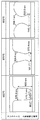
図3(a)は、(1)の工程を行ったときの断面図である。まず、トレンチゲート構造を形成し、半導体の表面、つまりp型ベース領域3やn+型ソース領域4びコンタクト領域3aの表面に形成されたゲート絶縁膜7やゲート電極8の上に、層間絶縁膜10を成膜する。層間絶縁膜10としては、流動性のある酸化膜となるPBSGを用いているが、BPSGの他、PSG(phospho silicate glassの略)、やBSG(Boron silicate glassの略)を用いることもできる。
図3(b)は、(2)の工程を行ったときの断面図である。この工程では、(1)の工程によって形成したコンタクトホール10aの底部に金属シリサイド9aを形成する。まず、(1)の工程から(2)の工程に至るまでの間に、コンタクトホール10aの底面に自然酸化膜が形成されている可能性があることから、HF(フッ酸)を用いて自然酸化膜をエッチングする。そして、コンタクトホール10a内を含めて層間絶縁膜10の上にNi膜を成膜したのち、例えば600〜750℃の加熱による1回目の金属シンターを行い、コンタクトホール10aの底面のSiC中に存在するSiとNi膜中のNiとをシリサイド化反応させる。これにより、Ni−Siにて構成される金属シリサイド9aが形成される。
図3(c)は、(3)の工程を行ったときの断面図である。図示しないが層間絶縁膜10の上に図示しないフォトレジストを成膜したのち、露光および現像を行い、さらにUV照射を行うことでフォトレジストをパターニングする。これにより、フォトレジストのうちコンタクトホール10bの形成予定領域が開口させられ、フォトレジストによるマスクが形成される。そして、このフォトレジストによるマスクを用いて、層間絶縁膜10をエッチングすることで、層間絶縁膜10に対してゲートパッド31のためのコンタクトホール10bを形成する。
図3(d)は、(4)の工程を行ったときの断面図である。まず、(3)の工程から(4)の工程に至るまでの間に、コンタクトホール10a、10bの底面に自然酸化膜が形成されている可能性があることから、HFを用いて自然酸化膜をエッチングする。そして、コンタクトホール10a、10b内を含めて層間絶縁膜10の上にスパッタリング等によってTi/TiN膜を成膜する。これにより、バリアメタル9b、31aを形成するための金属膜が形成される。
第2実施形態について説明する。本実施形態は、第1実施形態に対してH2アニールの工程順序を変更したものであり、その他については第1実施形態と同様であるため、第1実施形態と異なる部分についてのみ説明する。
本発明は上記した実施形態に限定されるものではなく、特許請求の範囲に記載した範囲内において適宜変更が可能である。
4 n+型ソース領域
9 ソース電極
9a 金属シリサイド
9b、31a バリアメタル
9c、31b Wプラグ
9d、31c Al−Si層
10 層間絶縁膜
10a、10b コンタクトホール
Claims (13)
- 半導体素子が形成された半導体(1〜5)と、
前記半導体の上に形成され、前記半導体素子に繋がるコンタクトホール(10a)を有し、リンとボロンの少なくとも一方を含んで構成された層間絶縁膜(10)と、
前記層間絶縁膜の上に形成され、前記コンタクトホールを通じて前記半導体素子と接続される金属電極(9d)と、を有し、
前記層間絶縁膜内に水素が充填されており、
さらに、前記層間絶縁膜にはリンが含まれており、該層間絶縁膜内においてリン濃度分布の極大値がある半導体装置。 - 半導体素子が形成された半導体(1〜5)と、
前記半導体の上に形成され、前記半導体素子に繋がるコンタクトホール(10a)を有し、リンとボロンの少なくとも一方を含んで構成された層間絶縁膜(10)と、
前記層間絶縁膜の上に形成され、前記コンタクトホールを通じて前記半導体素子と接続される金属電極(9d)と、を有し、
前記層間絶縁膜内に水素が充填されており、
前記層間絶縁膜内における水素濃度が1×1020cm−3以上であって、
前記層間絶縁膜にはリンが含まれており、該層間絶縁膜内においてリン濃度分布の極大値がある半導体装置。 - 前記層間絶縁膜内の全域においてリン濃度が2wt%以上である請求項1または2に記載の半導体装置。
- 前記層間絶縁膜にはボロンが含まれており、該層間絶縁膜内の全域においてボロン濃度が2wt%である請求項1ないし3のいずれか1つに記載の半導体装置。
- 前記コンタクトホール中には、タングステンプラグ(9c)が埋め込まれており、前記金属電極の下地面が平坦とされている請求項1ないし4のいずれか1つに記載の半導体装置。
- 前記コンタクトホールは、上面形状が正方形で構成され、該正方形の一辺の長さが0.3〜0.6μmとされていて、前記層間絶縁膜の底面と該コンタクトホールの側面との成す角度を側壁角として、該側壁角が85°以上である請求項1ないし5のいずれか1つに記載の半導体装置。
- 前記コンタクトホールは、上面形状が長方形のライン状で構成され、該長方形の短辺の長さが0.3〜0.6μmとされていて、前記層間絶縁膜の底面と該コンタクトホールの側面との成す角度を側壁角として、該側壁角が85°以上である請求項1ないし5のいずれか1つに記載の半導体装置。
- 前記半導体のうち前記半導体素子が形成されたセル部と、該セル部を囲むガードリング部を含む外周部とを有し、前記ガードリング部において前記半導体に凹部(20)が形成されていて、前記セル部と前記ガードリング部との間において段差が構成されており、
前記層間絶縁膜は、前記段差も覆うように形成されている請求項1ないし7のいずれか1つに記載の半導体装置。 - 前記半導体と前記層間絶縁膜との間には、前記層間絶縁膜よりも水素濃度が低い下地絶縁膜(7)が形成されている請求項1ないし8のいずれか1つに記載の半導体装置。
- 前記下地絶縁膜の水素濃度は1×1020cm−3未満である請求項9に記載の半導体装置。
- 前記層間絶縁膜と前記下地絶縁膜との界面において、前記層間絶縁膜および前記下地絶縁膜の双方を含めた膜内における水素濃度が極大値となっている請求項9または10に記載の半導体装置。
- 前記半導体素子は、
前記半導体として、裏面側が第1導電型もしくは第2導電型の高濃度不純物層(1)とされていると共に表面側が前記高濃度不純物層よりも低不純物濃度とされた第1導電型のドリフト層(2)とされ、炭化珪素にて構成された半導体基板(1、2)と、前記ドリフト層の上に形成された第2導電型の炭化珪素からなるベース領域(3)と、前記ベース領域の上に形成され、前記ドリフト層よりも高不純物濃度の第1導電型の炭化珪素で構成されたソース領域(4)と、を有し、
さらに、前記ソース領域の表面から前記ベース領域よりも深くまで形成されたゲートトレンチ(6)内に形成され、該ゲートトレンチの内壁面に形成されたゲート絶縁膜(7)と、前記ゲート絶縁膜の上に形成されたゲート電極(8)と、を有して構成されたトレンチゲート構造と、
前記ソース領域および前記ベース領域に接続された第1電極(9)と、
前記高濃度不純物層に接続された第2電極(11)と、を有しており、
前記ゲート絶縁膜は、前記下地絶縁膜を構成しており、
前記金属電極は、前記第1電極に含まれている請求項9ないし11のいずれか1つに記載の半導体装置。 - 半導体素子が形成された半導体(1〜5)と、
前記半導体の上に形成され、前記半導体素子に繋がるコンタクトホール(10a)を有し、リンとボロンの少なくとも一方を含んで構成された層間絶縁膜(10)と、
前記層間絶縁膜の上に形成され、前記コンタクトホールを通じて前記半導体素子と接続される金属電極(9d)と、を有し、
前記半導体のうち前記半導体素子が形成されたセル部と、該セル部を囲むガードリング部を含む外周部とを有し、前記ガードリング部において前記半導体に凹部(20)が形成されていて、前記セル部と前記ガードリング部との間において段差が構成されており、
前記層間絶縁膜が前記段差も覆うように形成される半導体装置の製造方法であって、
前記凹部が形成されることで前記段差が構成された前記半導体の上に前記層間絶縁膜を成膜することと、
リフローを行うことで、前記層間絶縁膜を流動させ、前記段差を所定の膜厚の前記層間絶縁膜で覆うことと、
前記段差を所定の膜厚の前記層間絶縁膜で覆うことの後に、前記コンタクトホールを形成することと、
前記コンタクトホールを形成することの後に、水素アニールを870℃以上で行うことで、前記層間絶縁膜内に水素を充填して該層間絶縁膜の緻密化処理を行うことと、を含んでいる半導体装置の製造方法。
Priority Applications (4)
| Application Number | Priority Date | Filing Date | Title |
|---|---|---|---|
| JP2017006002A JP6828449B2 (ja) | 2017-01-17 | 2017-01-17 | 半導体装置およびその製造方法 |
| CN201880006937.6A CN110235229B (zh) | 2017-01-17 | 2018-01-17 | 半导体装置及其制造方法 |
| PCT/JP2018/001260 WO2018135541A1 (ja) | 2017-01-17 | 2018-01-17 | 半導体装置およびその製造方法 |
| US16/511,345 US10923395B2 (en) | 2017-01-17 | 2019-07-15 | Semiconductor device and manufacturing method of semiconductor device |
Applications Claiming Priority (1)
| Application Number | Priority Date | Filing Date | Title |
|---|---|---|---|
| JP2017006002A JP6828449B2 (ja) | 2017-01-17 | 2017-01-17 | 半導体装置およびその製造方法 |
Publications (3)
| Publication Number | Publication Date |
|---|---|
| JP2018117016A JP2018117016A (ja) | 2018-07-26 |
| JP2018117016A5 JP2018117016A5 (ja) | 2019-04-25 |
| JP6828449B2 true JP6828449B2 (ja) | 2021-02-10 |
Family
ID=62908552
Family Applications (1)
| Application Number | Title | Priority Date | Filing Date |
|---|---|---|---|
| JP2017006002A Active JP6828449B2 (ja) | 2017-01-17 | 2017-01-17 | 半導体装置およびその製造方法 |
Country Status (4)
| Country | Link |
|---|---|
| US (1) | US10923395B2 (ja) |
| JP (1) | JP6828449B2 (ja) |
| CN (1) | CN110235229B (ja) |
| WO (1) | WO2018135541A1 (ja) |
Families Citing this family (11)
| Publication number | Priority date | Publication date | Assignee | Title |
|---|---|---|---|---|
| WO2019069580A1 (ja) * | 2017-10-05 | 2019-04-11 | 富士電機株式会社 | 半導体装置 |
| JPWO2020031971A1 (ja) * | 2018-08-07 | 2021-08-10 | ローム株式会社 | SiC半導体装置 |
| JP7188230B2 (ja) * | 2019-03-28 | 2022-12-13 | 株式会社デンソー | 半導体装置 |
| JP7443673B2 (ja) * | 2019-04-15 | 2024-03-06 | 富士電機株式会社 | 炭化珪素半導体装置 |
| JP7081564B2 (ja) * | 2019-04-24 | 2022-06-07 | 株式会社デンソー | 半導体装置とその製造方法 |
| JP7472435B2 (ja) * | 2019-05-13 | 2024-04-23 | 富士電機株式会社 | 半導体モジュールの製造方法 |
| CN112466923A (zh) * | 2019-09-06 | 2021-03-09 | 富士电机株式会社 | 半导体装置 |
| JP7404722B2 (ja) * | 2019-09-06 | 2023-12-26 | 富士電機株式会社 | 半導体装置 |
| JP7129397B2 (ja) | 2019-12-06 | 2022-09-01 | ローム株式会社 | SiC半導体装置 |
| JP2022168904A (ja) * | 2021-04-27 | 2022-11-09 | 富士電機株式会社 | 炭化珪素半導体装置および炭化珪素半導体装置の製造方法 |
| CN114583013A (zh) * | 2022-03-10 | 2022-06-03 | 常州时创能源股份有限公司 | 一种bsg去除方法 |
Family Cites Families (21)
| Publication number | Priority date | Publication date | Assignee | Title |
|---|---|---|---|---|
| JPH0456222A (ja) * | 1990-06-25 | 1992-02-24 | Matsushita Electron Corp | 半導体装置の製造方法 |
| JPH0582781A (ja) * | 1991-09-24 | 1993-04-02 | Nec Yamagata Ltd | 半導体集積回路装置 |
| JPH06177129A (ja) * | 1992-12-09 | 1994-06-24 | Oki Electric Ind Co Ltd | 半導体装置の製造方法 |
| JP2757782B2 (ja) * | 1994-06-30 | 1998-05-25 | 日本電気株式会社 | 半導体装置の製造方法 |
| JP3543504B2 (ja) * | 1996-08-06 | 2004-07-14 | ソニー株式会社 | 半導体装置の製造方法 |
| JP2002134607A (ja) * | 2000-10-20 | 2002-05-10 | Hitachi Ltd | 半導体集積回路装置の製造方法 |
| DE112004003004T5 (de) * | 2004-10-25 | 2007-10-25 | Spansion Llc, Sunnyvale | Halbleiterbauelement und Verfahren zu dessen Herstellung |
| JP2007096263A (ja) | 2005-08-31 | 2007-04-12 | Denso Corp | 炭化珪素半導体装置およびその製造方法。 |
| KR100872981B1 (ko) * | 2007-07-19 | 2008-12-08 | 주식회사 동부하이텍 | 반도체 소자의 제조방법 |
| EP2091083A3 (en) | 2008-02-13 | 2009-10-14 | Denso Corporation | Silicon carbide semiconductor device including a deep layer |
| JP2010165778A (ja) * | 2009-01-14 | 2010-07-29 | Sharp Corp | 半導体装置の製造方法 |
| JP5813303B2 (ja) | 2009-11-20 | 2015-11-17 | 株式会社日立国際電気 | 半導体装置の製造方法、基板処理方法および基板処理装置 |
| JP5770892B2 (ja) * | 2009-11-20 | 2015-08-26 | 株式会社日立国際電気 | 半導体装置の製造方法、基板処理方法および基板処理装置 |
| KR101995682B1 (ko) * | 2011-03-18 | 2019-07-02 | 가부시키가이샤 한도오따이 에네루기 켄큐쇼 | 산화물 반도체막, 반도체 장치, 및 반도체 장치의 제작 방법 |
| JP2013041919A (ja) | 2011-08-12 | 2013-02-28 | Renesas Electronics Corp | 半導体装置の製造方法 |
| JP6245723B2 (ja) | 2012-04-27 | 2017-12-13 | 富士電機株式会社 | 炭化珪素半導体装置の製造方法 |
| JP2014027076A (ja) * | 2012-07-26 | 2014-02-06 | Renesas Electronics Corp | 半導体装置 |
| JP6160477B2 (ja) * | 2013-12-25 | 2017-07-12 | トヨタ自動車株式会社 | 半導体装置 |
| WO2016080269A1 (ja) * | 2014-11-17 | 2016-05-26 | 富士電機株式会社 | 半導体装置および半導体装置の製造方法 |
| DE112016000071T5 (de) * | 2015-02-03 | 2017-03-23 | Fuji Electric Co., Ltd. | Halbleitervorrichtung und Verfahren zu ihrer Herstellung |
| JP6409681B2 (ja) | 2015-05-29 | 2018-10-24 | 株式会社デンソー | 半導体装置およびその製造方法 |
-
2017
- 2017-01-17 JP JP2017006002A patent/JP6828449B2/ja active Active
-
2018
- 2018-01-17 CN CN201880006937.6A patent/CN110235229B/zh active Active
- 2018-01-17 WO PCT/JP2018/001260 patent/WO2018135541A1/ja active Application Filing
-
2019
- 2019-07-15 US US16/511,345 patent/US10923395B2/en active Active
Also Published As
| Publication number | Publication date |
|---|---|
| CN110235229B (zh) | 2022-08-12 |
| US10923395B2 (en) | 2021-02-16 |
| JP2018117016A (ja) | 2018-07-26 |
| WO2018135541A1 (ja) | 2018-07-26 |
| US20190341308A1 (en) | 2019-11-07 |
| CN110235229A (zh) | 2019-09-13 |
Similar Documents
| Publication | Publication Date | Title |
|---|---|---|
| JP6828449B2 (ja) | 半導体装置およびその製造方法 | |
| JP6341074B2 (ja) | 半導体装置の製造方法 | |
| JP6354525B2 (ja) | 炭化珪素半導体装置の製造方法 | |
| JP4913336B2 (ja) | 半導体装置 | |
| CN106549003A (zh) | 贯穿衬底通孔结构及其制造方法 | |
| US10707343B2 (en) | Method of manufacturing semiconductor device and semiconductor device | |
| CN103151377A (zh) | 横向晶体管组件及其制造方法 | |
| US10825909B2 (en) | Method of manufacturing semiconductor device and semiconductor device | |
| JP7369601B2 (ja) | 半導体装置およびその製造方法 | |
| WO2015174197A1 (ja) | 半導体装置および半導体装置の製造方法 | |
| JP7069605B2 (ja) | 半導体装置の製造方法 | |
| JP2008182106A (ja) | 半導体装置 | |
| CN108292668A (zh) | 半导体器件及其制造方法 | |
| JP2010103208A (ja) | 半導体装置 | |
| JP4860122B2 (ja) | 半導体装置の製造方法 | |
| JP2002314081A (ja) | トレンチゲート型半導体装置およびその製造方法 | |
| US9698103B2 (en) | Semiconductor device and manufacturing method therefor | |
| JP2013509729A (ja) | 半導体素子 | |
| JP6750590B2 (ja) | 炭化珪素半導体装置 | |
| CN105830203B (zh) | 半导体装置 | |
| JP4744103B2 (ja) | 抵抗素子を含む半導体装置及びその製造方法 | |
| JP2013098228A (ja) | 半導体装置およびその製造方法 | |
| JPWO2017126084A1 (ja) | 半導体装置 | |
| JP6648743B2 (ja) | 炭化珪素半導体装置の製造方法 | |
| JP6623824B2 (ja) | 半導体装置およびその製造方法 |
Legal Events
| Date | Code | Title | Description |
|---|---|---|---|
| A521 | Request for written amendment filed |
Free format text: JAPANESE INTERMEDIATE CODE: A523 Effective date: 20190315 |
|
| A621 | Written request for application examination |
Free format text: JAPANESE INTERMEDIATE CODE: A621 Effective date: 20190315 |
|
| A131 | Notification of reasons for refusal |
Free format text: JAPANESE INTERMEDIATE CODE: A131 Effective date: 20200526 |
|
| A521 | Request for written amendment filed |
Free format text: JAPANESE INTERMEDIATE CODE: A523 Effective date: 20200724 |
|
| A711 | Notification of change in applicant |
Free format text: JAPANESE INTERMEDIATE CODE: A711 Effective date: 20200807 |
|
| A521 | Request for written amendment filed |
Free format text: JAPANESE INTERMEDIATE CODE: A821 Effective date: 20200807 |
|
| TRDD | Decision of grant or rejection written | ||
| A01 | Written decision to grant a patent or to grant a registration (utility model) |
Free format text: JAPANESE INTERMEDIATE CODE: A01 Effective date: 20201222 |
|
| A61 | First payment of annual fees (during grant procedure) |
Free format text: JAPANESE INTERMEDIATE CODE: A61 Effective date: 20210104 |
|
| R150 | Certificate of patent or registration of utility model |
Ref document number: 6828449 Country of ref document: JP Free format text: JAPANESE INTERMEDIATE CODE: R150 |
|
| R250 | Receipt of annual fees |
Free format text: JAPANESE INTERMEDIATE CODE: R250 |