JP6828449B2 - Semiconductor devices and their manufacturing methods - Google Patents
Semiconductor devices and their manufacturing methods Download PDFInfo
- Publication number
- JP6828449B2 JP6828449B2 JP2017006002A JP2017006002A JP6828449B2 JP 6828449 B2 JP6828449 B2 JP 6828449B2 JP 2017006002 A JP2017006002 A JP 2017006002A JP 2017006002 A JP2017006002 A JP 2017006002A JP 6828449 B2 JP6828449 B2 JP 6828449B2
- Authority
- JP
- Japan
- Prior art keywords
- insulating film
- interlayer insulating
- semiconductor
- contact hole
- semiconductor device
- Prior art date
- Legal status (The legal status is an assumption and is not a legal conclusion. Google has not performed a legal analysis and makes no representation as to the accuracy of the status listed.)
- Active
Links
- 239000004065 semiconductor Substances 0.000 title claims description 119
- 238000004519 manufacturing process Methods 0.000 title claims description 21
- 239000011229 interlayer Substances 0.000 claims description 123
- 239000010410 layer Substances 0.000 claims description 72
- 239000002184 metal Substances 0.000 claims description 51
- 229910052751 metal Inorganic materials 0.000 claims description 51
- 238000000137 annealing Methods 0.000 claims description 48
- 229910052739 hydrogen Inorganic materials 0.000 claims description 39
- 239000001257 hydrogen Substances 0.000 claims description 39
- UFHFLCQGNIYNRP-UHFFFAOYSA-N Hydrogen Chemical compound [H][H] UFHFLCQGNIYNRP-UHFFFAOYSA-N 0.000 claims description 35
- HBMJWWWQQXIZIP-UHFFFAOYSA-N silicon carbide Chemical compound [Si+]#[C-] HBMJWWWQQXIZIP-UHFFFAOYSA-N 0.000 claims description 30
- 229910010271 silicon carbide Inorganic materials 0.000 claims description 30
- 239000000758 substrate Substances 0.000 claims description 21
- OAICVXFJPJFONN-UHFFFAOYSA-N Phosphorus Chemical compound [P] OAICVXFJPJFONN-UHFFFAOYSA-N 0.000 claims description 20
- 239000012535 impurity Substances 0.000 claims description 20
- 229910052698 phosphorus Inorganic materials 0.000 claims description 20
- 239000011574 phosphorus Substances 0.000 claims description 20
- ZOXJGFHDIHLPTG-UHFFFAOYSA-N Boron Chemical compound [B] ZOXJGFHDIHLPTG-UHFFFAOYSA-N 0.000 claims description 17
- 229910052796 boron Inorganic materials 0.000 claims description 17
- 238000000280 densification Methods 0.000 claims description 13
- 238000000034 method Methods 0.000 claims description 12
- 238000009826 distribution Methods 0.000 claims description 10
- 230000002093 peripheral effect Effects 0.000 claims description 8
- 239000012528 membrane Substances 0.000 claims description 4
- WFKWXMTUELFFGS-UHFFFAOYSA-N tungsten Chemical compound [W] WFKWXMTUELFFGS-UHFFFAOYSA-N 0.000 claims description 2
- 229910052721 tungsten Inorganic materials 0.000 claims description 2
- 239000010937 tungsten Substances 0.000 claims description 2
- 239000005380 borophosphosilicate glass Substances 0.000 description 36
- 229910018125 Al-Si Inorganic materials 0.000 description 26
- 229910018520 Al—Si Inorganic materials 0.000 description 26
- BOTDANWDWHJENH-UHFFFAOYSA-N Tetraethyl orthosilicate Chemical compound CCO[Si](OCC)(OCC)OCC BOTDANWDWHJENH-UHFFFAOYSA-N 0.000 description 17
- 229910021332 silicide Inorganic materials 0.000 description 17
- FVBUAEGBCNSCDD-UHFFFAOYSA-N silicide(4-) Chemical compound [Si-4] FVBUAEGBCNSCDD-UHFFFAOYSA-N 0.000 description 17
- PXHVJJICTQNCMI-UHFFFAOYSA-N nickel Substances [Ni] PXHVJJICTQNCMI-UHFFFAOYSA-N 0.000 description 14
- 229920002120 photoresistant polymer Polymers 0.000 description 14
- 230000004888 barrier function Effects 0.000 description 11
- 239000000463 material Substances 0.000 description 10
- 238000005530 etching Methods 0.000 description 9
- 229910052710 silicon Inorganic materials 0.000 description 9
- 229910018557 Si O Inorganic materials 0.000 description 7
- ATJFFYVFTNAWJD-UHFFFAOYSA-N Tin Chemical compound [Sn] ATJFFYVFTNAWJD-UHFFFAOYSA-N 0.000 description 7
- 239000012530 fluid Substances 0.000 description 7
- 238000010438 heat treatment Methods 0.000 description 7
- LIVNPJMFVYWSIS-UHFFFAOYSA-N silicon monoxide Inorganic materials [Si-]#[O+] LIVNPJMFVYWSIS-UHFFFAOYSA-N 0.000 description 7
- 239000002344 surface layer Substances 0.000 description 7
- 239000010936 titanium Substances 0.000 description 7
- 229910004298 SiO 2 Inorganic materials 0.000 description 6
- 230000008859 change Effects 0.000 description 6
- 230000000694 effects Effects 0.000 description 6
- 238000007747 plating Methods 0.000 description 6
- 238000012360 testing method Methods 0.000 description 6
- 238000009792 diffusion process Methods 0.000 description 5
- 238000002474 experimental method Methods 0.000 description 5
- 238000005259 measurement Methods 0.000 description 5
- 230000008018 melting Effects 0.000 description 5
- 238000002844 melting Methods 0.000 description 5
- 230000008569 process Effects 0.000 description 5
- 230000001681 protective effect Effects 0.000 description 5
- 230000015572 biosynthetic process Effects 0.000 description 4
- 230000020169 heat generation Effects 0.000 description 4
- 150000002739 metals Chemical class 0.000 description 4
- 230000007246 mechanism Effects 0.000 description 3
- IJGRMHOSHXDMSA-UHFFFAOYSA-N Atomic nitrogen Chemical compound N#N IJGRMHOSHXDMSA-UHFFFAOYSA-N 0.000 description 2
- KRHYYFGTRYWZRS-UHFFFAOYSA-N Fluorane Chemical compound F KRHYYFGTRYWZRS-UHFFFAOYSA-N 0.000 description 2
- 239000004642 Polyimide Substances 0.000 description 2
- 238000005229 chemical vapour deposition Methods 0.000 description 2
- 230000003247 decreasing effect Effects 0.000 description 2
- 239000007772 electrode material Substances 0.000 description 2
- 238000011156 evaluation Methods 0.000 description 2
- 150000002431 hydrogen Chemical class 0.000 description 2
- 125000004435 hydrogen atom Chemical group [H]* 0.000 description 2
- 229910052759 nickel Inorganic materials 0.000 description 2
- 239000005360 phosphosilicate glass Substances 0.000 description 2
- 229920001721 polyimide Polymers 0.000 description 2
- 238000004544 sputter deposition Methods 0.000 description 2
- 238000009281 ultraviolet germicidal irradiation Methods 0.000 description 2
- 229910018098 Ni-Si Inorganic materials 0.000 description 1
- 229910018529 Ni—Si Inorganic materials 0.000 description 1
- RTAQQCXQSZGOHL-UHFFFAOYSA-N Titanium Chemical compound [Ti] RTAQQCXQSZGOHL-UHFFFAOYSA-N 0.000 description 1
- 150000001875 compounds Chemical class 0.000 description 1
- 238000011161 development Methods 0.000 description 1
- 230000005684 electric field Effects 0.000 description 1
- 238000009413 insulation Methods 0.000 description 1
- 238000005468 ion implantation Methods 0.000 description 1
- 239000000155 melt Substances 0.000 description 1
- 229910052757 nitrogen Inorganic materials 0.000 description 1
- 238000000059 patterning Methods 0.000 description 1
- 230000035515 penetration Effects 0.000 description 1
- 229910021420 polycrystalline silicon Inorganic materials 0.000 description 1
- 239000002994 raw material Substances 0.000 description 1
- 230000000630 rising effect Effects 0.000 description 1
- 239000005368 silicate glass Substances 0.000 description 1
- 239000010703 silicon Substances 0.000 description 1
- 229910000679 solder Inorganic materials 0.000 description 1
- -1 that is Substances 0.000 description 1
- 229910052719 titanium Inorganic materials 0.000 description 1
Images


Classifications
-
- H—ELECTRICITY
- H01—ELECTRIC ELEMENTS
- H01L—SEMICONDUCTOR DEVICES NOT COVERED BY CLASS H10
- H01L21/00—Processes or apparatus adapted for the manufacture or treatment of semiconductor or solid state devices or of parts thereof
- H01L21/70—Manufacture or treatment of devices consisting of a plurality of solid state components formed in or on a common substrate or of parts thereof; Manufacture of integrated circuit devices or of parts thereof
- H01L21/71—Manufacture of specific parts of devices defined in group H01L21/70
- H01L21/768—Applying interconnections to be used for carrying current between separate components within a device comprising conductors and dielectrics
- H01L21/76897—Formation of self-aligned vias or contact plugs, i.e. involving a lithographically uncritical step
-
- H—ELECTRICITY
- H01—ELECTRIC ELEMENTS
- H01L—SEMICONDUCTOR DEVICES NOT COVERED BY CLASS H10
- H01L21/00—Processes or apparatus adapted for the manufacture or treatment of semiconductor or solid state devices or of parts thereof
- H01L21/02—Manufacture or treatment of semiconductor devices or of parts thereof
- H01L21/02104—Forming layers
- H01L21/02107—Forming insulating materials on a substrate
- H01L21/02109—Forming insulating materials on a substrate characterised by the type of layer, e.g. type of material, porous/non-porous, pre-cursors, mixtures or laminates
- H01L21/02112—Forming insulating materials on a substrate characterised by the type of layer, e.g. type of material, porous/non-porous, pre-cursors, mixtures or laminates characterised by the material of the layer
- H01L21/02123—Forming insulating materials on a substrate characterised by the type of layer, e.g. type of material, porous/non-porous, pre-cursors, mixtures or laminates characterised by the material of the layer the material containing silicon
- H01L21/02126—Forming insulating materials on a substrate characterised by the type of layer, e.g. type of material, porous/non-porous, pre-cursors, mixtures or laminates characterised by the material of the layer the material containing silicon the material containing Si, O, and at least one of H, N, C, F, or other non-metal elements, e.g. SiOC, SiOC:H or SiONC
- H01L21/02129—Forming insulating materials on a substrate characterised by the type of layer, e.g. type of material, porous/non-porous, pre-cursors, mixtures or laminates characterised by the material of the layer the material containing silicon the material containing Si, O, and at least one of H, N, C, F, or other non-metal elements, e.g. SiOC, SiOC:H or SiONC the material being boron or phosphorus doped silicon oxides, e.g. BPSG, BSG or PSG
-
- H—ELECTRICITY
- H01—ELECTRIC ELEMENTS
- H01L—SEMICONDUCTOR DEVICES NOT COVERED BY CLASS H10
- H01L21/00—Processes or apparatus adapted for the manufacture or treatment of semiconductor or solid state devices or of parts thereof
- H01L21/02—Manufacture or treatment of semiconductor devices or of parts thereof
- H01L21/02104—Forming layers
- H01L21/02107—Forming insulating materials on a substrate
- H01L21/02296—Forming insulating materials on a substrate characterised by the treatment performed before or after the formation of the layer
- H01L21/02318—Forming insulating materials on a substrate characterised by the treatment performed before or after the formation of the layer post-treatment
- H01L21/02321—Forming insulating materials on a substrate characterised by the treatment performed before or after the formation of the layer post-treatment introduction of substances into an already existing insulating layer
-
- H—ELECTRICITY
- H01—ELECTRIC ELEMENTS
- H01L—SEMICONDUCTOR DEVICES NOT COVERED BY CLASS H10
- H01L21/00—Processes or apparatus adapted for the manufacture or treatment of semiconductor or solid state devices or of parts thereof
- H01L21/02—Manufacture or treatment of semiconductor devices or of parts thereof
- H01L21/02104—Forming layers
- H01L21/02107—Forming insulating materials on a substrate
- H01L21/02296—Forming insulating materials on a substrate characterised by the treatment performed before or after the formation of the layer
- H01L21/02318—Forming insulating materials on a substrate characterised by the treatment performed before or after the formation of the layer post-treatment
- H01L21/02337—Forming insulating materials on a substrate characterised by the treatment performed before or after the formation of the layer post-treatment treatment by exposure to a gas or vapour
-
- H—ELECTRICITY
- H01—ELECTRIC ELEMENTS
- H01L—SEMICONDUCTOR DEVICES NOT COVERED BY CLASS H10
- H01L21/00—Processes or apparatus adapted for the manufacture or treatment of semiconductor or solid state devices or of parts thereof
- H01L21/02—Manufacture or treatment of semiconductor devices or of parts thereof
- H01L21/04—Manufacture or treatment of semiconductor devices or of parts thereof the devices having potential barriers, e.g. a PN junction, depletion layer or carrier concentration layer
- H01L21/18—Manufacture or treatment of semiconductor devices or of parts thereof the devices having potential barriers, e.g. a PN junction, depletion layer or carrier concentration layer the devices having semiconductor bodies comprising elements of Group IV of the Periodic Table or AIIIBV compounds with or without impurities, e.g. doping materials
- H01L21/28—Manufacture of electrodes on semiconductor bodies using processes or apparatus not provided for in groups H01L21/20 - H01L21/268
-
- H—ELECTRICITY
- H01—ELECTRIC ELEMENTS
- H01L—SEMICONDUCTOR DEVICES NOT COVERED BY CLASS H10
- H01L21/00—Processes or apparatus adapted for the manufacture or treatment of semiconductor or solid state devices or of parts thereof
- H01L21/02—Manufacture or treatment of semiconductor devices or of parts thereof
- H01L21/04—Manufacture or treatment of semiconductor devices or of parts thereof the devices having potential barriers, e.g. a PN junction, depletion layer or carrier concentration layer
- H01L21/18—Manufacture or treatment of semiconductor devices or of parts thereof the devices having potential barriers, e.g. a PN junction, depletion layer or carrier concentration layer the devices having semiconductor bodies comprising elements of Group IV of the Periodic Table or AIIIBV compounds with or without impurities, e.g. doping materials
- H01L21/30—Treatment of semiconductor bodies using processes or apparatus not provided for in groups H01L21/20 - H01L21/26
- H01L21/31—Treatment of semiconductor bodies using processes or apparatus not provided for in groups H01L21/20 - H01L21/26 to form insulating layers thereon, e.g. for masking or by using photolithographic techniques; After treatment of these layers; Selection of materials for these layers
- H01L21/3105—After-treatment
- H01L21/3115—Doping the insulating layers
-
- H—ELECTRICITY
- H01—ELECTRIC ELEMENTS
- H01L—SEMICONDUCTOR DEVICES NOT COVERED BY CLASS H10
- H01L23/00—Details of semiconductor or other solid state devices
- H01L23/52—Arrangements for conducting electric current within the device in operation from one component to another, i.e. interconnections, e.g. wires, lead frames
- H01L23/522—Arrangements for conducting electric current within the device in operation from one component to another, i.e. interconnections, e.g. wires, lead frames including external interconnections consisting of a multilayer structure of conductive and insulating layers inseparably formed on the semiconductor body
- H01L23/532—Arrangements for conducting electric current within the device in operation from one component to another, i.e. interconnections, e.g. wires, lead frames including external interconnections consisting of a multilayer structure of conductive and insulating layers inseparably formed on the semiconductor body characterised by the materials
- H01L23/5329—Insulating materials
-
- H—ELECTRICITY
- H01—ELECTRIC ELEMENTS
- H01L—SEMICONDUCTOR DEVICES NOT COVERED BY CLASS H10
- H01L29/00—Semiconductor devices specially adapted for rectifying, amplifying, oscillating or switching and having potential barriers; Capacitors or resistors having potential barriers, e.g. a PN-junction depletion layer or carrier concentration layer; Details of semiconductor bodies or of electrodes thereof ; Multistep manufacturing processes therefor
- H01L29/02—Semiconductor bodies ; Multistep manufacturing processes therefor
- H01L29/06—Semiconductor bodies ; Multistep manufacturing processes therefor characterised by their shape; characterised by the shapes, relative sizes, or dispositions of the semiconductor regions ; characterised by the concentration or distribution of impurities within semiconductor regions
- H01L29/0603—Semiconductor bodies ; Multistep manufacturing processes therefor characterised by their shape; characterised by the shapes, relative sizes, or dispositions of the semiconductor regions ; characterised by the concentration or distribution of impurities within semiconductor regions characterised by particular constructional design considerations, e.g. for preventing surface leakage, for controlling electric field concentration or for internal isolations regions
- H01L29/0607—Semiconductor bodies ; Multistep manufacturing processes therefor characterised by their shape; characterised by the shapes, relative sizes, or dispositions of the semiconductor regions ; characterised by the concentration or distribution of impurities within semiconductor regions characterised by particular constructional design considerations, e.g. for preventing surface leakage, for controlling electric field concentration or for internal isolations regions for preventing surface leakage or controlling electric field concentration
- H01L29/0611—Semiconductor bodies ; Multistep manufacturing processes therefor characterised by their shape; characterised by the shapes, relative sizes, or dispositions of the semiconductor regions ; characterised by the concentration or distribution of impurities within semiconductor regions characterised by particular constructional design considerations, e.g. for preventing surface leakage, for controlling electric field concentration or for internal isolations regions for preventing surface leakage or controlling electric field concentration for increasing or controlling the breakdown voltage of reverse biased devices
- H01L29/0615—Semiconductor bodies ; Multistep manufacturing processes therefor characterised by their shape; characterised by the shapes, relative sizes, or dispositions of the semiconductor regions ; characterised by the concentration or distribution of impurities within semiconductor regions characterised by particular constructional design considerations, e.g. for preventing surface leakage, for controlling electric field concentration or for internal isolations regions for preventing surface leakage or controlling electric field concentration for increasing or controlling the breakdown voltage of reverse biased devices by the doping profile or the shape or the arrangement of the PN junction, or with supplementary regions, e.g. junction termination extension [JTE]
- H01L29/0619—Semiconductor bodies ; Multistep manufacturing processes therefor characterised by their shape; characterised by the shapes, relative sizes, or dispositions of the semiconductor regions ; characterised by the concentration or distribution of impurities within semiconductor regions characterised by particular constructional design considerations, e.g. for preventing surface leakage, for controlling electric field concentration or for internal isolations regions for preventing surface leakage or controlling electric field concentration for increasing or controlling the breakdown voltage of reverse biased devices by the doping profile or the shape or the arrangement of the PN junction, or with supplementary regions, e.g. junction termination extension [JTE] with a supplementary region doped oppositely to or in rectifying contact with the semiconductor containing or contacting region, e.g. guard rings with PN or Schottky junction
-
- H—ELECTRICITY
- H01—ELECTRIC ELEMENTS
- H01L—SEMICONDUCTOR DEVICES NOT COVERED BY CLASS H10
- H01L29/00—Semiconductor devices specially adapted for rectifying, amplifying, oscillating or switching and having potential barriers; Capacitors or resistors having potential barriers, e.g. a PN-junction depletion layer or carrier concentration layer; Details of semiconductor bodies or of electrodes thereof ; Multistep manufacturing processes therefor
- H01L29/02—Semiconductor bodies ; Multistep manufacturing processes therefor
- H01L29/06—Semiconductor bodies ; Multistep manufacturing processes therefor characterised by their shape; characterised by the shapes, relative sizes, or dispositions of the semiconductor regions ; characterised by the concentration or distribution of impurities within semiconductor regions
- H01L29/0657—Semiconductor bodies ; Multistep manufacturing processes therefor characterised by their shape; characterised by the shapes, relative sizes, or dispositions of the semiconductor regions ; characterised by the concentration or distribution of impurities within semiconductor regions characterised by the shape of the body
- H01L29/0661—Semiconductor bodies ; Multistep manufacturing processes therefor characterised by their shape; characterised by the shapes, relative sizes, or dispositions of the semiconductor regions ; characterised by the concentration or distribution of impurities within semiconductor regions characterised by the shape of the body specially adapted for altering the breakdown voltage by removing semiconductor material at, or in the neighbourhood of, a reverse biased junction, e.g. by bevelling, moat etching, depletion etching
-
- H—ELECTRICITY
- H01—ELECTRIC ELEMENTS
- H01L—SEMICONDUCTOR DEVICES NOT COVERED BY CLASS H10
- H01L29/00—Semiconductor devices specially adapted for rectifying, amplifying, oscillating or switching and having potential barriers; Capacitors or resistors having potential barriers, e.g. a PN-junction depletion layer or carrier concentration layer; Details of semiconductor bodies or of electrodes thereof ; Multistep manufacturing processes therefor
- H01L29/02—Semiconductor bodies ; Multistep manufacturing processes therefor
- H01L29/06—Semiconductor bodies ; Multistep manufacturing processes therefor characterised by their shape; characterised by the shapes, relative sizes, or dispositions of the semiconductor regions ; characterised by the concentration or distribution of impurities within semiconductor regions
- H01L29/0684—Semiconductor bodies ; Multistep manufacturing processes therefor characterised by their shape; characterised by the shapes, relative sizes, or dispositions of the semiconductor regions ; characterised by the concentration or distribution of impurities within semiconductor regions characterised by the shape, relative sizes or dispositions of the semiconductor regions or junctions between the regions
- H01L29/0692—Surface layout
- H01L29/0696—Surface layout of cellular field-effect devices, e.g. multicellular DMOS transistors or IGBTs
-
- H—ELECTRICITY
- H01—ELECTRIC ELEMENTS
- H01L—SEMICONDUCTOR DEVICES NOT COVERED BY CLASS H10
- H01L29/00—Semiconductor devices specially adapted for rectifying, amplifying, oscillating or switching and having potential barriers; Capacitors or resistors having potential barriers, e.g. a PN-junction depletion layer or carrier concentration layer; Details of semiconductor bodies or of electrodes thereof ; Multistep manufacturing processes therefor
- H01L29/02—Semiconductor bodies ; Multistep manufacturing processes therefor
- H01L29/06—Semiconductor bodies ; Multistep manufacturing processes therefor characterised by their shape; characterised by the shapes, relative sizes, or dispositions of the semiconductor regions ; characterised by the concentration or distribution of impurities within semiconductor regions
- H01L29/10—Semiconductor bodies ; Multistep manufacturing processes therefor characterised by their shape; characterised by the shapes, relative sizes, or dispositions of the semiconductor regions ; characterised by the concentration or distribution of impurities within semiconductor regions with semiconductor regions connected to an electrode not carrying current to be rectified, amplified or switched and such electrode being part of a semiconductor device which comprises three or more electrodes
- H01L29/1095—Body region, i.e. base region, of DMOS transistors or IGBTs
-
- H—ELECTRICITY
- H01—ELECTRIC ELEMENTS
- H01L—SEMICONDUCTOR DEVICES NOT COVERED BY CLASS H10
- H01L29/00—Semiconductor devices specially adapted for rectifying, amplifying, oscillating or switching and having potential barriers; Capacitors or resistors having potential barriers, e.g. a PN-junction depletion layer or carrier concentration layer; Details of semiconductor bodies or of electrodes thereof ; Multistep manufacturing processes therefor
- H01L29/02—Semiconductor bodies ; Multistep manufacturing processes therefor
- H01L29/12—Semiconductor bodies ; Multistep manufacturing processes therefor characterised by the materials of which they are formed
- H01L29/16—Semiconductor bodies ; Multistep manufacturing processes therefor characterised by the materials of which they are formed including, apart from doping materials or other impurities, only elements of Group IV of the Periodic Table
- H01L29/1608—Silicon carbide
-
- H—ELECTRICITY
- H01—ELECTRIC ELEMENTS
- H01L—SEMICONDUCTOR DEVICES NOT COVERED BY CLASS H10
- H01L29/00—Semiconductor devices specially adapted for rectifying, amplifying, oscillating or switching and having potential barriers; Capacitors or resistors having potential barriers, e.g. a PN-junction depletion layer or carrier concentration layer; Details of semiconductor bodies or of electrodes thereof ; Multistep manufacturing processes therefor
- H01L29/40—Electrodes ; Multistep manufacturing processes therefor
- H01L29/41—Electrodes ; Multistep manufacturing processes therefor characterised by their shape, relative sizes or dispositions
- H01L29/417—Electrodes ; Multistep manufacturing processes therefor characterised by their shape, relative sizes or dispositions carrying the current to be rectified, amplified or switched
- H01L29/41725—Source or drain electrodes for field effect devices
- H01L29/41741—Source or drain electrodes for field effect devices for vertical or pseudo-vertical devices
-
- H—ELECTRICITY
- H01—ELECTRIC ELEMENTS
- H01L—SEMICONDUCTOR DEVICES NOT COVERED BY CLASS H10
- H01L29/00—Semiconductor devices specially adapted for rectifying, amplifying, oscillating or switching and having potential barriers; Capacitors or resistors having potential barriers, e.g. a PN-junction depletion layer or carrier concentration layer; Details of semiconductor bodies or of electrodes thereof ; Multistep manufacturing processes therefor
- H01L29/40—Electrodes ; Multistep manufacturing processes therefor
- H01L29/41—Electrodes ; Multistep manufacturing processes therefor characterised by their shape, relative sizes or dispositions
- H01L29/423—Electrodes ; Multistep manufacturing processes therefor characterised by their shape, relative sizes or dispositions not carrying the current to be rectified, amplified or switched
- H01L29/42312—Gate electrodes for field effect devices
- H01L29/42316—Gate electrodes for field effect devices for field-effect transistors
- H01L29/4232—Gate electrodes for field effect devices for field-effect transistors with insulated gate
- H01L29/42356—Disposition, e.g. buried gate electrode
- H01L29/4236—Disposition, e.g. buried gate electrode within a trench, e.g. trench gate electrode, groove gate electrode
-
- H—ELECTRICITY
- H01—ELECTRIC ELEMENTS
- H01L—SEMICONDUCTOR DEVICES NOT COVERED BY CLASS H10
- H01L29/00—Semiconductor devices specially adapted for rectifying, amplifying, oscillating or switching and having potential barriers; Capacitors or resistors having potential barriers, e.g. a PN-junction depletion layer or carrier concentration layer; Details of semiconductor bodies or of electrodes thereof ; Multistep manufacturing processes therefor
- H01L29/66—Types of semiconductor device ; Multistep manufacturing processes therefor
- H01L29/66007—Multistep manufacturing processes
- H01L29/66053—Multistep manufacturing processes of devices having a semiconductor body comprising crystalline silicon carbide
- H01L29/66068—Multistep manufacturing processes of devices having a semiconductor body comprising crystalline silicon carbide the devices being controllable only by the electric current supplied or the electric potential applied, to an electrode which does not carry the current to be rectified, amplified or switched, e.g. three-terminal devices
-
- H—ELECTRICITY
- H01—ELECTRIC ELEMENTS
- H01L—SEMICONDUCTOR DEVICES NOT COVERED BY CLASS H10
- H01L29/00—Semiconductor devices specially adapted for rectifying, amplifying, oscillating or switching and having potential barriers; Capacitors or resistors having potential barriers, e.g. a PN-junction depletion layer or carrier concentration layer; Details of semiconductor bodies or of electrodes thereof ; Multistep manufacturing processes therefor
- H01L29/66—Types of semiconductor device ; Multistep manufacturing processes therefor
- H01L29/66007—Multistep manufacturing processes
- H01L29/66075—Multistep manufacturing processes of devices having semiconductor bodies comprising group 14 or group 13/15 materials
- H01L29/66227—Multistep manufacturing processes of devices having semiconductor bodies comprising group 14 or group 13/15 materials the devices being controllable only by the electric current supplied or the electric potential applied, to an electrode which does not carry the current to be rectified, amplified or switched, e.g. three-terminal devices
- H01L29/66234—Bipolar junction transistors [BJT]
- H01L29/66325—Bipolar junction transistors [BJT] controlled by field-effect, e.g. insulated gate bipolar transistors [IGBT]
- H01L29/66333—Vertical insulated gate bipolar transistors
- H01L29/66348—Vertical insulated gate bipolar transistors with a recessed gate
-
- H—ELECTRICITY
- H01—ELECTRIC ELEMENTS
- H01L—SEMICONDUCTOR DEVICES NOT COVERED BY CLASS H10
- H01L29/00—Semiconductor devices specially adapted for rectifying, amplifying, oscillating or switching and having potential barriers; Capacitors or resistors having potential barriers, e.g. a PN-junction depletion layer or carrier concentration layer; Details of semiconductor bodies or of electrodes thereof ; Multistep manufacturing processes therefor
- H01L29/66—Types of semiconductor device ; Multistep manufacturing processes therefor
- H01L29/68—Types of semiconductor device ; Multistep manufacturing processes therefor controllable by only the electric current supplied, or only the electric potential applied, to an electrode which does not carry the current to be rectified, amplified or switched
- H01L29/70—Bipolar devices
- H01L29/72—Transistor-type devices, i.e. able to continuously respond to applied control signals
- H01L29/739—Transistor-type devices, i.e. able to continuously respond to applied control signals controlled by field-effect, e.g. bipolar static induction transistors [BSIT]
- H01L29/7393—Insulated gate bipolar mode transistors, i.e. IGBT; IGT; COMFET
- H01L29/7395—Vertical transistors, e.g. vertical IGBT
- H01L29/7396—Vertical transistors, e.g. vertical IGBT with a non planar surface, e.g. with a non planar gate or with a trench or recess or pillar in the surface of the emitter, base or collector region for improving current density or short circuiting the emitter and base regions
- H01L29/7397—Vertical transistors, e.g. vertical IGBT with a non planar surface, e.g. with a non planar gate or with a trench or recess or pillar in the surface of the emitter, base or collector region for improving current density or short circuiting the emitter and base regions and a gate structure lying on a slanted or vertical surface or formed in a groove, e.g. trench gate IGBT
-
- H—ELECTRICITY
- H01—ELECTRIC ELEMENTS
- H01L—SEMICONDUCTOR DEVICES NOT COVERED BY CLASS H10
- H01L29/00—Semiconductor devices specially adapted for rectifying, amplifying, oscillating or switching and having potential barriers; Capacitors or resistors having potential barriers, e.g. a PN-junction depletion layer or carrier concentration layer; Details of semiconductor bodies or of electrodes thereof ; Multistep manufacturing processes therefor
- H01L29/66—Types of semiconductor device ; Multistep manufacturing processes therefor
- H01L29/68—Types of semiconductor device ; Multistep manufacturing processes therefor controllable by only the electric current supplied, or only the electric potential applied, to an electrode which does not carry the current to be rectified, amplified or switched
- H01L29/76—Unipolar devices, e.g. field effect transistors
- H01L29/772—Field effect transistors
- H01L29/78—Field effect transistors with field effect produced by an insulated gate
- H01L29/7801—DMOS transistors, i.e. MISFETs with a channel accommodating body or base region adjoining a drain drift region
- H01L29/7802—Vertical DMOS transistors, i.e. VDMOS transistors
- H01L29/7811—Vertical DMOS transistors, i.e. VDMOS transistors with an edge termination structure
-
- H—ELECTRICITY
- H01—ELECTRIC ELEMENTS
- H01L—SEMICONDUCTOR DEVICES NOT COVERED BY CLASS H10
- H01L29/00—Semiconductor devices specially adapted for rectifying, amplifying, oscillating or switching and having potential barriers; Capacitors or resistors having potential barriers, e.g. a PN-junction depletion layer or carrier concentration layer; Details of semiconductor bodies or of electrodes thereof ; Multistep manufacturing processes therefor
- H01L29/66—Types of semiconductor device ; Multistep manufacturing processes therefor
- H01L29/68—Types of semiconductor device ; Multistep manufacturing processes therefor controllable by only the electric current supplied, or only the electric potential applied, to an electrode which does not carry the current to be rectified, amplified or switched
- H01L29/76—Unipolar devices, e.g. field effect transistors
- H01L29/772—Field effect transistors
- H01L29/78—Field effect transistors with field effect produced by an insulated gate
- H01L29/7801—DMOS transistors, i.e. MISFETs with a channel accommodating body or base region adjoining a drain drift region
- H01L29/7802—Vertical DMOS transistors, i.e. VDMOS transistors
- H01L29/7813—Vertical DMOS transistors, i.e. VDMOS transistors with trench gate electrode, e.g. UMOS transistors
Landscapes
- Engineering & Computer Science (AREA)
- Microelectronics & Electronic Packaging (AREA)
- Power Engineering (AREA)
- General Physics & Mathematics (AREA)
- Computer Hardware Design (AREA)
- Physics & Mathematics (AREA)
- Condensed Matter Physics & Semiconductors (AREA)
- Ceramic Engineering (AREA)
- Manufacturing & Machinery (AREA)
- Chemical & Material Sciences (AREA)
- Crystallography & Structural Chemistry (AREA)
- Internal Circuitry In Semiconductor Integrated Circuit Devices (AREA)
- Electrodes Of Semiconductors (AREA)
- Formation Of Insulating Films (AREA)
Description
本発明は、層間絶縁膜に形成されるコンタクトホールを通じて金属電極との電気的接続が行われる半導体素子が備えられた半導体装置およびその製造方法に関し、特に炭化珪素(以下、SiCという)半導体装置に適用されて好適なものである。 The present invention relates to a semiconductor device provided with a semiconductor element that is electrically connected to a metal electrode through a contact hole formed in an interlayer insulating film and a method for manufacturing the same, and particularly for a silicon carbide (hereinafter referred to as SiC) semiconductor device. It is applicable and suitable.
従来より、MOSFETやショットキーダイオード等の半導体素子が形成されるセル部と、セル部の周囲を囲むガードリング部とが備えられる半導体装置がある。この半導体装置では、半導体素子が形成された半導体の上に層間絶縁膜が形成されると共に、層間絶縁膜に形成されたコンタクトホールを通じて金属電極が配置されることで、半導体素子と金属電極との電気的接続が行われる。 Conventionally, there is a semiconductor device provided with a cell portion in which a semiconductor element such as a MOSFET or a Schottky diode is formed, and a guard ring portion surrounding the periphery of the cell portion. In this semiconductor device, an interlayer insulating film is formed on the semiconductor on which the semiconductor element is formed, and a metal electrode is arranged through a contact hole formed in the interlayer insulating film, whereby the semiconductor element and the metal electrode are separated from each other. An electrical connection is made.
層間絶縁膜としては様々な材質のものを選択することができるが、例えば流動性のある絶縁膜となるBPSG(Boro-phospho silicate glassの略)などが用いられることがある。BPSGなどはリフローによって容易に流動する流動性を有した材質であることから、半導体の表面に絶縁膜を成膜した後に、絶縁膜の膜厚の均一化を行うような場合に適している。例えば、特許文献1に示されるような外周領域に凹部を設けることでセル領域を突出させたメサ構造のように、段差を有する半導体の表面を層間絶縁膜で覆う場合が挙げられる。このような構造においては、層間絶縁膜を成膜したときに段差部の側面での膜厚が薄くなるため、層間絶縁膜としてBPSG等の流動性のある絶縁膜が用いられ、リフローによって流動させることで段差部の側面での膜厚を確保している。
Various materials can be selected as the interlayer insulating film, and for example, BPSG (abbreviation of Boro-phospho silicate glass), which is a fluid insulating film, may be used. Since BPSG and the like are materials having fluidity that easily flows by reflow, they are suitable for cases where the film thickness of the insulating film is made uniform after the insulating film is formed on the surface of the semiconductor. For example, there is a case where the surface of a semiconductor having a step is covered with an interlayer insulating film, such as a mesa structure in which a cell region is projected by providing a recess in an outer peripheral region as shown in
しかしながら、本発明者らが半導体装置の製造後に短絡耐量試験を行ったところ、半導体素子に備えられる絶縁膜、例えばMOSFETにおけるゲート絶縁膜にクラックが入り、所望の短絡耐量が得られないことがあった。これは、以下のメカニズムに因ると推定される。 However, when the present inventors conducted a short-circuit tolerance test after manufacturing the semiconductor device, the insulating film provided in the semiconductor element, for example, the gate insulating film in the MOSFET may be cracked and the desired short-circuit tolerance may not be obtained. It was. This is presumed to be due to the following mechanism.
例えば、半導体素子としてMOSFETが形成された半導体の上にBPSGで構成される層間絶縁膜を形成し、コンタクトホールを形成した後にAl−Si膜にて構成される金属電極を形成して短絡耐量試験を行っている。短絡耐量試験では、ソース−ドレイン間に1000Vを印加したときに、ゲート電極への誤信号によって半導体素子がオンしたときの短絡耐量を測定する。 For example, a short-circuit tolerance test is performed by forming an interlayer insulating film composed of BPSG on a semiconductor on which a MOSFET is formed as a semiconductor element, forming a contact hole, and then forming a metal electrode composed of an Al—Si film. It is carried out. In the short-circuit tolerance test, when 1000 V is applied between the source and drain, the short-circuit tolerance when the semiconductor element is turned on by an erroneous signal to the gate electrode is measured.
このような短絡耐量試験を行ったときに、大電流が流れることで半導体素子が発熱する。例えば、MOSFETの場合、MOSFETの半導体部において発熱が生じる。この熱が金属電極に伝わると、Alを主原料とする金属電極の材料の融点が低いことから、金属電極が溶融する。この溶融した金属電極は半導体素子がオフされたときに固まるが、この固まるときに層間絶縁膜に対して応力を加え、それが更にゲート絶縁膜にも伝わって、ゲート絶縁膜にクラックを発生させる。もしくは、半導体素子がオンオフによって発熱冷却されるときに金属電極が伸縮し、層間絶縁膜に対して応力を加えるために、それがゲート絶縁膜にも伝わって、ゲート絶縁膜にクラックを発生させる。このようなメカニズムによってゲート絶縁膜にクラックを生じさせ、例えばゲート−ソース間が短絡することで短絡耐量が得られなくなると推定される。 When such a short-circuit tolerance test is performed, a large current flows and the semiconductor element generates heat. For example, in the case of MOSFET, heat is generated in the semiconductor part of MOSFET. When this heat is transferred to the metal electrode, the metal electrode melts because the melting point of the metal electrode material containing Al as the main raw material is low. The molten metal electrode hardens when the semiconductor element is turned off. When the semiconductor element hardens, stress is applied to the interlayer insulating film, which is further transmitted to the gate insulating film to cause cracks in the gate insulating film. .. Alternatively, when the semiconductor element is heated and cooled by turning on and off, the metal electrode expands and contracts, and stress is applied to the interlayer insulating film, which is also transmitted to the gate insulating film to cause cracks in the gate insulating film. It is presumed that such a mechanism causes cracks in the gate insulating film, and for example, a short circuit between the gate and the source makes it impossible to obtain a short circuit tolerance.
そして、BPSGのように流動性がある材料で層間絶縁膜を形成した場合、コンタクトホールの側壁の角部が丸められ、開口部の入口の寸法が底部よりも広がることから、上記のように発生する応力が大きくなり、より短絡耐量を低下させていることが判った。 When the interlayer insulating film is formed of a fluid material such as BPSG, the corners of the side wall of the contact hole are rounded and the size of the entrance of the opening is wider than that of the bottom, which is generated as described above. It was found that the stress applied increased and the short-circuit tolerance was further reduced.
したがって、BPSGのように流動性がある材料を用いて層間絶縁膜を形成する場合においても、半導体素子の短絡耐量が得られるようにすることが望まれる。特に、SiC半導体装置では、大電流が用いられることから、半導体素子での発熱が大きくなり易く、短絡耐量の低下の課題が生じ易い。 Therefore, even when the interlayer insulating film is formed by using a fluid material such as BPSG, it is desired that the short-circuit tolerance of the semiconductor element can be obtained. In particular, in a SiC semiconductor device, since a large current is used, heat generation in the semiconductor element tends to be large, and a problem of lowering the short-circuit tolerance tends to occur.
なお、ここでは短絡耐量の低下についての課題を例に挙げて説明したが、層間絶縁膜のコンタクトホールの側壁の角部が丸められることによって発生する応力が要因となって、様々な課題が発生することが確認されている。例えば、試料を低温下と高温下に繰り返し晒す冷熱サイクル試験や半導体素子のオンオフを繰り返し行って温度変化させることを繰り返すパワーサイクル試験においても、上記応力が要因となって半導体装置の耐久性を低下させていることが確認されている。 Although the problem of lowering the short-circuit tolerance has been described here as an example, various problems occur due to the stress generated by rounding the corners of the side wall of the contact hole of the interlayer insulating film. It has been confirmed that For example, in a thermal cycle test in which a sample is repeatedly exposed to a low temperature and a high temperature, or in a power cycle test in which a semiconductor element is repeatedly turned on and off to change the temperature, the above stress causes a decrease in the durability of the semiconductor device. It has been confirmed that it is being used.
本発明は上記点に鑑みて、流動性がある材料を用いて層間絶縁膜を形成する場合において、コンタクトホールの角部が丸まることを抑制し、耐久性を向上することが可能な半導体装置およびその製造方法を提供することを目的とする。 In view of the above points, the present invention provides a semiconductor device capable of suppressing rounding of corners of contact holes and improving durability when an interlayer insulating film is formed using a fluid material. It is an object of the present invention to provide the manufacturing method.
上記目的を達成するため、請求項1〜12に記載の半導体装置は、半導体素子が形成された半導体(1〜5)と、半導体の上に形成され、半導体素子に繋がるコンタクトホール(10a)を有し、リンとボロンの少なくとも一方を含んで構成された層間絶縁膜(10)と、層間絶縁膜の上に形成され、コンタクトホールを通じて半導体素子と接続される金属電極(9d)と、を有し、層間絶縁膜内に水素が充填されている。
In order to achieve the above object, the semiconductor device according to
このように、層間絶縁膜内に水素を充填することで層間絶縁膜を緻密化している。このような緻密化が行われた層間絶縁膜は、緻密化を行っていない場合と比較して固くなる。このため、層間絶縁膜に対してコンタクトホールを形成した後に高温となる加熱工程が行われても、コンタクトホールの側壁の角部が丸まることが抑制され、側壁が切り立ったコンタクトホールにできる。これにより、金属電極のコンタクトホール内への入り込み量が多くても、応力に基づく層間絶縁膜の変形が抑制される。したがって、半導体装置の耐久性を向上することが可能となる。 In this way, the interlayer insulating film is densified by filling the interlayer insulating film with hydrogen. The interlayer insulating film in which such densification is performed becomes harder than in the case where densification is not performed. Therefore, even if a heating step of increasing the temperature is performed after forming the contact hole in the interlayer insulating film, the corners of the side wall of the contact hole are suppressed from being rounded, and the contact hole can be formed with a steep side wall. As a result, even if the amount of the metal electrode entering the contact hole is large, the deformation of the interlayer insulating film due to stress is suppressed. Therefore, it is possible to improve the durability of the semiconductor device.
請求項13に記載の半導体装置の製造方法では、凹部が形成されることで段差が構成された半導体の上に層間絶縁膜を成膜することと、リフローを行うことで、層間絶縁膜を流動させ、段差を所定の膜厚の層間絶縁膜で覆うことと、段差を所定の膜厚の層間絶縁膜で覆うことの後に、コンタクトホールを形成することと、コンタクトホールを形成することの後に、H2アニールを870℃以上で行うことで、層間絶縁膜内に水素を充填して該層間絶縁膜の緻密化処理を行うことと、を含んでいる。 In the method for manufacturing a semiconductor device according to claim 13 , an interlayer insulating film is formed on a semiconductor having a step formed by forming a recess, and a reflow is performed to flow the interlayer insulating film. After forming a contact hole after covering the step with an interlayer insulating film having a predetermined film thickness and covering the step with an interlayer insulating film having a predetermined film thickness, and after forming the contact hole, By performing H 2 annealing at 870 ° C. or higher, the interlayer insulating film is filled with hydrogen and the interlayer insulating film is densified.
このように、コンタクトホールを形成した後にH2アニールを行うことで、層間絶縁膜に水素を充填して層間絶縁膜の緻密化処理を行うことができる。これにより、層間絶縁膜に対してコンタクトホールを形成した後に高温となる加熱工程が行われても、コンタクトホールの側壁の角部が丸まるとが抑制され、側壁が切り立ったコンタクトホールにできる。したがって、耐久性を向上することが可能な半導体装置を製造することができる。 By performing H 2 annealing after forming the contact hole in this way , the interlayer insulating film can be filled with hydrogen and the interlayer insulating film can be densified. As a result, even if a heating step of increasing the temperature is performed after forming the contact hole in the interlayer insulating film, the corners of the side wall of the contact hole are prevented from being rounded, and the contact hole can be formed with a steep side wall. Therefore, it is possible to manufacture a semiconductor device capable of improving durability.
なお、上記各手段の括弧内の符号は、後述する実施形態に記載の具体的手段との対応関係の一例を示すものである。 The reference numerals in parentheses of each of the above means indicate an example of the correspondence with the specific means described in the embodiment described later.
以下、本発明の実施形態について図に基づいて説明する。なお、以下の各実施形態相互において、互いに同一もしくは均等である部分には、同一符号を付して説明を行う。 Hereinafter, embodiments of the present invention will be described with reference to the drawings. In each of the following embodiments, parts that are the same or equal to each other will be described with the same reference numerals.
(第1実施形態)
第1実施形態について説明する。ここでは半導体装置として、トレンチゲート構造の反転型のMOSFETを半導体素子とするSiC半導体装置を例に挙げて説明する。
(First Embodiment)
The first embodiment will be described. Here, as a semiconductor device, a SiC semiconductor device using an inverted MOSFET having a trench gate structure as a semiconductor element will be described as an example.
図1に示すように、SiC半導体装置は、トレンチゲート構造のMOSFETが形成されるセル部と、このセル部を囲む外周部とを有した構成とされている。外周部は、ガードリング部と、ガードリング部よりも内側、つまりセル部とガードリング部との間に配置される繋ぎ部とを有した構成とされている。 As shown in FIG. 1, the SiC semiconductor device has a configuration having a cell portion in which a MOSFET having a trench gate structure is formed and an outer peripheral portion surrounding the cell portion. The outer peripheral portion has a configuration having a guard ring portion and a connecting portion arranged inside the guard ring portion, that is, between the cell portion and the guard ring portion.
SiC半導体装置は、SiCからなる高濃度不純物層を構成するn+型基板1の表面側に、n+型基板1よりも低不純物濃度のSiCからなるn-型ドリフト層2がエピタキシャル成長させられた半導体基板を用いて形成されている。つまり、裏面側がn+型基板1による高濃度不純物層、表面側がそれよりも低不純物濃度とされたn-型ドリフト層2とされた半導体基板が用いられている。そして、n-型ドリフト層2の上に、p型ベース領域3がエピタキシャル成長させられ、さらにp型ベース領域3の表層部にn+型ソース領域4が形成されている。
SiC semiconductor device, the surface side of the n + -
n+型基板1は、例えばn型不純物濃度が1.0×10¹⁹/cm3とされ、表面が(0001)Si面とされている。n-型ドリフト層2は、n+型基板1よりも低不純物濃度で構成され、例えばn型不純物濃度が0.5〜2.0×1016/cm3とされている。
n + -
また、p型ベース領域3は、チャネル領域が形成される部分で、p型不純物濃度が例えば2.0×10¹⁷/cm3程度とされ、厚みが300nmで構成されている。n+型ソース領域4は、n-型ドリフト層2よりも高不純物濃度とされ、表層部におけるn型不純物濃度が例えば2.5×1018〜1.0×1019/cm3、厚さ0.5μm程度で構成されている。
Further, the p-
セル部および繋ぎ部では、n+型基板1の表面側においてp型ベース領域3が残されており、ガードリング部では、p型ベース領域3を貫通してn-型ドリフト層2に達するように凹部20が形成されている。このような構造とすることでメサ構造が構成されている。
In the cell portion and the connecting portion, the p-
また、セル部および繋ぎ部では、p型ベース領域3の表面にp型高濃度層によって構成されるコンタクト領域3aが形成されている。
Further, in the cell portion and the connecting portion, a
さらに、セル部では、p型ベース領域3よりも下方、つまりn-型ドリフト層2の表層部にp型ディープ層5が形成されている。p型ディープ層5は、p型ベース領域3よりもp型不純物濃度が高くされている。p型ディープ層5は、図1の紙面垂直方向、すなわち後述するトレンチゲート構造と同方向を長手方向として延設されている。具体的には、p型ディープ層5は、n-型ドリフト層2に複数本が等間隔に配置され、互いに交点なく離れて配置されたストライプ状のトレンチ5a内に備えられている。例えば、各p型ディープ層5は、p型不純物濃度が例えば1.0×10¹⁷〜1.0×1019cm3、幅0.7μm、深さ2.0μm程度で構成されている。
Further, in the cell portion, the p-type
また、p型ベース領域3およびn+型ソース領域4を貫通してn-型ドリフト層2に達するように、例えば幅が0.8μm、深さが1.0μmのゲートトレンチ6が形成されている。このゲートトレンチ6の側面と接するように上述したp型ベース領域3およびn+型ソース領域4が配置されている。ゲートトレンチ6は、図1の紙面左右方向を幅方向、紙面垂直方向を長手方向、紙面上下方向を深さ方向とするライン状のレイアウトで形成され、複数本が平行に等間隔で並べられることでストライプ状とされている。
Further, a
さらに、p型ベース領域3のうちゲートトレンチ6の側面に位置している部分を、縦型MOSFETの作動時にn+型ソース領域4とn-型ドリフト層2との間を繋ぐチャネル領域として、チャネル領域を含むゲートトレンチ6の内壁面にはゲート絶縁膜7が形成されている。ゲート絶縁膜7は、例えば熱酸化膜などによって形成されている。そして、ゲート絶縁膜7の表面にはドープドPoly−Siにて構成されたゲート電極8が形成されており、これらゲート絶縁膜7およびゲート電極8によってゲートトレンチ6内が埋め尽くされている。
Further, the portion of the p-
なお、ゲート絶縁膜7は、ゲートトレンチ6の内壁面以外の表面にも形成されている。具体的には、n+型ソース領域4の表面の一部や、繋ぎ部におけるp型ベース領域3の表面にも形成されている。また、ゲート電極8についても、繋ぎ部におけるゲート絶縁膜7の表面上まで延設されている。
The
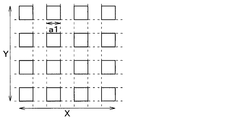
また、n+型ソース領域4およびコンタクト領域3aの表面は、第1電極に相当するソース電極9に接続されている。同様に、ゲート電極8は、繋ぎ部に延設された部分において、ゲートパッド31に接続されている。これらソース電極9およびゲートパッド31は、ゲート絶縁膜7などの上に形成された層間絶縁膜10を介してMOSFETの各構成要素が形成された半導体上に形成されており、層間絶縁膜10に形成されたコンタクトホール10a、10bを通じて各構成要素と接続されている。ソース電極9およびゲートパッド31は、複数の金属で構成されている。コンタクトホール10a、10bのパターンについては任意であり、例えば複数の正方形のものを配列させたパターン、長方形の短ライン状のものを配列させたパターン、もしくは、ライン状のものを並べたパターンなどが挙げられる。
Further, the surfaces of the n +
ソース電極9は、次のように構成されている。具体的には、ソース電極9のうちn+型ソース領域4およびコンタクト領域3aとの接触箇所には、Ni(ニッケル)等の金属を用いて形成した金属シリサイド9aが形成されている。その上には、Ti(チタン)やTiN等で構成されるバリアメタル9bが形成され、さらにその上に、W(タングステン)プラグ9cおよびAlを主成分とするAl−Si層9dが形成されている。また、Al−Si層9dの表面にはNiメッキ層9eを介してAu層9fが形成されている。
The source electrode 9 is configured as follows. Specifically, a
一方、ゲートパッド31は、次のように構成されている。具体的には、ゲートパッド31のうち、ゲート電極8との接触箇所には、TiN等で構成されるバリアメタル31aが形成され、さらにその上に、Wプラグ31bおよびAlを主成分とするAl−Si層31cが形成されている。なお、ここでは図示していないが、Al−Si層31cの表面にも、Niメッキ層を介してAu層を形成しても良い。
On the other hand, the
金属シリサイド9aは、n+型ソース領域4およびコンタクト領域3aとソース電極9との間の接触抵抗の低減のために備えられている。
The
バリアメタル9b、31aは、Al−Si層9d、31cに含まれるAlが半導体側や層間絶縁膜10側に拡散することを抑制する役割を果たす。また、バリアメタル9bについては、金属シリサイド9a内のNiがAl−Si層9d側に拡散することを抑制する役割も果たす。
The
Wプラグ9c、31bは、Al−Si層9d、31cの下地面の平坦化を行って層間絶縁膜10に形成されたコンタクトホール10a、10b内へのAl−Si層9d、31cの入り込みを少なくする役割を果たす。また、Wプラグ9c、31bは、Alよりも融点が高い材料でコンタクトホール10a、10b内を埋め込む役割も果たす。コンタクトホール10a、10b内へのAl−Si層9d、31cの入り込みを少なくすると、Al−Si層9d、31cが伸縮する際、もしくは、発熱によって溶融してから固化する際に、平坦面上で伸縮もしくは固化するだけとなる。このため、層間絶縁膜10に対して加えられる応力が抑制される。また、Wの融点がAlよりも高いことから、コンタクトホール10a、10b内にWプラグ9c、31bを配置しても、半導体素子の発熱によって溶融することが生じにくいため、溶融してから固化するという現象が発生することを抑制できる。よって、層間絶縁膜10に対して加えられる応力が更に抑制される。
In the W plugs 9c and 31b, the lower ground of the Al—Si layers 9d and 31c is flattened to reduce the penetration of the Al—Si layers 9d and 31c into the
Al−Si層9d、31cは、一般的な電極材料として用いられるものであり、金属電極に相当するものである。ここでは金属電極をAi−Si層9d、31cで構成しているが、Alのみで構成するなど、他のAlを主成分とする材料で構成しても良い。基本的には、ソース電極9やゲートパッド31をAlを主成分とするAl−Si層9d、31cのみで構成できると好ましい。しかしながら、Alの拡散などを考慮して、Al−Si層9d、31cのみでなく、他の材料を共に用いてソース電極9やゲートパッド31を構成している。
The Al—Si layers 9d and 31c are used as general electrode materials and correspond to metal electrodes. Here, the metal electrode is composed of Ai-
Niメッキ層9eおよびAu層9fは、ソース電極9を通じて外部との接続を図る際のはんだ濡れ性を向上させるために形成されている。
The Ni plating layer 9e and the
さらに、n+型基板1の裏面側にはn+型基板1と電気的に接続された第2電極に相当するドレイン電極11が形成されている。このような構造により、nチャネルタイプの反転型のトレンチゲート構造のMOSFETが構成されている。そして、このようなMOSFETが複数セル配置されることでセル部が構成されている。
Further, on the back side of the n + -
一方、ガードリング部では、上記したように、n+型ソース領域4およびp型ベース領域3を貫通してn-型ドリフト層2に達するように凹部20が形成されている。このため、セル部から離れた位置ではn+型ソース領域4およびp型ベース領域3が除去されて、n-型ドリフト層2が露出させられている。そして、n+型SiC基板1の厚み方向において、凹部20よりも内側に位置するセル部や繋ぎ部が島状に突き出したメサ部となっており、セル部および繋ぎ部とガードリング部との間において段差が構成されている。
On the other hand, in the guard ring portion, as described above, the
また、凹部20の下方に位置するn-型ドリフト層2の表層部には、セル部を囲むように、複数本のp型ガードリング21が備えられている。半導体基板の表面に対する法線(以下、基板法線方向という)から見て、p型ガードリング21の上面レイアウトは、四隅が丸められた四角形状や円形状などとされている。p型ガードリング21は、例えばn-型ドリフト層2の表層部に形成されたトレンチ21a内に配置され、エピタキシャル成長によるp型のエピタキシャル膜によって構成されている。
Further, a plurality of p-type guard rings 21 are provided on the surface layer portion of the n -
なお、図示していないが、必要に応じてp型ガードリング21よりも外周にEQR構造が備えられることにより、セル部を囲む外周耐圧構造が備えられたガードリング部が構成されている。
Although not shown, a guard ring portion having an outer peripheral pressure resistant structure surrounding the cell portion is configured by providing an EQR structure on the outer periphery of the p-
また、セル部からガードリング部に至るまでの間を繋ぎ部として、繋ぎ部およびガードリング部の内周側において、n-型ドリフト層2の表層部にp型リサーフ層30が形成されている。例えば、基板法線方向から見て、セル部を囲むように繋ぎ部が形成されており、さらに繋ぎ部の外側を囲むように、四隅が丸められた四角形状のp型ガードリング21が複数本形成されている。p型リサーフ層30は、セル部の周りを囲みつつ、ガードリング部に至るように延設されている。このp型リサーフ層30も、n型ドリフト層2の表層部に形成したトレンチ30a内に配置され、エピタキシャル成長によるp型のエピタキシャル膜によって構成されている。
Further, a p-
このようなp型リサーフ層30を形成することで、等電位線をガードリング部側に導くことができ、繋ぎ部内で電界集中する部位が発生しないようにできるため、耐圧低下を抑制することが可能となる。
By forming such a p-
さらに、このように構成されるセル部、繋ぎ部およびガードリング部を覆うように、ポリイミド等によって構成される保護膜40が形成されている。そして、図1に示すようにソース電極9が保護膜40から露出されると共に、図1とは別断面においてゲートパッド31が保護膜40から露出された構成とされている。
Further, a
以上のような構造により、本実施形態にかかるSiC半導体装置が構成されている。このように構成されるSiC半導体装置は、MOSFETをオンするときには、ゲート電極8への印加電圧を制御することでゲートトレンチ6の側面に位置するp型ベース領域3の表面部にチャネル領域を形成する。これにより、n+型ソース領域4およびn-型ドリフト層2を介して、ソース電極9およびドレイン電極11の間に電流を流す。
The SiC semiconductor device according to the present embodiment is configured by the above structure. When the MOSFET is turned on, the SiC semiconductor device configured in this way forms a channel region on the surface of the p-
また、逆バイアス時には、繋ぎ部では、p型リサーフ層30が形成されていることで等電位線のせり上がりが抑制されて、ガードリング部側に向かうようにされる。そして、ガードリング部では、p型ガードリング21によって等電位線の間隔が外周方向に向かって広がりながら終端させられるようになり、ガードリング部でも所望の耐圧を得ることができる。したがって、所望の耐圧を得ることが可能なSiC半導体装置とすることができる。
Further, at the time of reverse bias, the p-
続いて、本実施形態にかかるSiC半導体装置の製造方法について図2〜図3を参照して説明する。ただし、製造方法のうち、n+型基板1の上にn-型ドリフト層2を形成し、p型ディープ層5を形成してからp型ベース領域3およびn+型ソース領域4を形成したり、コンタクト領域3aを形成し、さらにトレンチゲート構造を形成する工程は従来と同様である。このため、従来と同様の工程以降の各工程について説明する。
Subsequently, a method for manufacturing the SiC semiconductor device according to the present embodiment will be described with reference to FIGS. 2 to 3. However, in the manufacturing method, the n -
図2に示す製造工程のフローチャートのように、(1)層間絶縁膜10およびソース電極9のコンタクトホール10aの形成工程、(2)シリサイド形成工程、(3)ゲートパッド31のコンタクトホール10bの形成工程、(4)電極形成工程を行う。以下、これら各工程を(1)〜(4)の工程として説明する。
As shown in the flowchart of the manufacturing process shown in FIG. 2, (1) the step of forming the
〔(1)の工程〕
図3(a)は、(1)の工程を行ったときの断面図である。まず、トレンチゲート構造を形成し、半導体の表面、つまりp型ベース領域3やn+型ソース領域4びコンタクト領域3aの表面に形成されたゲート絶縁膜7やゲート電極8の上に、層間絶縁膜10を成膜する。層間絶縁膜10としては、流動性のある酸化膜となるPBSGを用いているが、BPSGの他、PSG(phospho silicate glassの略)、やBSG(Boron silicate glassの略)を用いることもできる。
[Step (1)]
FIG. 3A is a cross-sectional view when the step (1) is performed. First, a trench gate structure is formed, and interlayer insulation is performed on the surface of the semiconductor, that is, the
次に、例えばN2(窒素)雰囲気でのリフロー、つまりN2アニールを行う。層間絶縁膜10を成膜したときには、凹部20によってセル部および繋ぎ部とガードリング部との間において段差が構成されている。このため、リフローを行うことで層間絶縁膜10を流動させ、段差部でも層間絶縁膜10が所望の膜厚となるようにする。このように、段差部が所望の膜厚の層間絶縁膜10によって覆われることで、段差部での耐圧も図ることが可能となる。
Next, for example, reflow in an N 2 (nitrogen) atmosphere, that is, N 2 annealing is performed. When the
この後、層間絶縁膜10について、流動性が小さくなって固くなるようにするための緻密化処理を行う。具体的には、水素雰囲気下において加熱処理することでH2アニールを行う。加熱処理の温度については、800℃以上としており、好ましくは870℃以上、例えば930℃以上としている。また、加熱処理の時間については、20分としている。このようなH2アニールを行うと、層間絶縁膜10を緻密化することが可能となる。このメカニズムについては明確となっていないが、例えば層間絶縁膜10をBPSGで構成する場合、水素が充填されることでSiO2になり切れていないSiやSi−Oと水素とが結び付き、結合力を強めることが可能になるためと推定される。すなわち、Hは、ダングリングボンドとしてSiやSi−Oの未結合手と容易に結合して分子間に入り込めるため、それにより未結合手が存在して結合が弱かった層間絶縁膜10の結合が強くなり、固まることで緻密化されると考えられる。
After that, the
このような緻密化処理を行ったのち、図示しないが層間絶縁膜10の上に図示しないフォトレジストを成膜してから露光および現像を行い、さらにUV(紫外線)照射を行うことでフォトレジストをパターニングする。これにより、フォトレジストのうちコンタクトホール10aの形成予定領域が開口させられ、フォトレジストによるマスクが形成される。そして、このフォトレジストによるマスクを用いて、層間絶縁膜10をエッチングすることで、層間絶縁膜10に対してソース電極9のためのコンタクトホール10aを形成する。
After performing such a densification treatment, a photoresist (not shown), which is not shown, is formed on the
〔(2)の工程〕
図3(b)は、(2)の工程を行ったときの断面図である。この工程では、(1)の工程によって形成したコンタクトホール10aの底部に金属シリサイド9aを形成する。まず、(1)の工程から(2)の工程に至るまでの間に、コンタクトホール10aの底面に自然酸化膜が形成されている可能性があることから、HF(フッ酸)を用いて自然酸化膜をエッチングする。そして、コンタクトホール10a内を含めて層間絶縁膜10の上にNi膜を成膜したのち、例えば600〜750℃の加熱による1回目の金属シンターを行い、コンタクトホール10aの底面のSiC中に存在するSiとNi膜中のNiとをシリサイド化反応させる。これにより、Ni−Siにて構成される金属シリサイド9aが形成される。
[Step (2)]
FIG. 3B is a cross-sectional view when the step (2) is performed. In this step, the
この後、エッチング液に浸漬することによってNi膜のうち金属シリサイド9aとされていない残部を除去し、金属シリサイド9aのみが残るようにする。そして、1回目の金属シンターよりも高温、例えば800〜900℃で2回目の金属シンターを行い、金属シリサイド9aを固める。これにより、金属シリサイド9aのさらなる低抵抗化を図ることができる。
After that, by immersing in an etching solution, the rest of the Ni film that is not the
なお、ここまでで説明した(2)の工程については、特に、半導体としてSiCを用いる場合に実施することが好ましい。しかしながら、(2)の工程中に高温処理が行われる工程が含まれることから、層間絶縁膜10を流動性のある材料で構成すると、層間絶縁膜10の流動によってコンタクトホール10aの側壁の角部が丸まり得る。
It is preferable that the step (2) described so far is carried out particularly when SiC is used as the semiconductor. However, since the step (2) includes a step of performing high temperature treatment, when the
これに対して、本実施形態では、高温処理が行われる工程の前に、層間絶縁膜10を流動性が小さくなって固くなるようにするための緻密化処理を行っている。このため、層間絶縁膜10が強固なものになっていることから、高温処理が行われても、層間絶縁膜10が丸まることを抑制できる。
On the other hand, in the present embodiment, before the step in which the high temperature treatment is performed, the
〔(3)の工程〕
図3(c)は、(3)の工程を行ったときの断面図である。図示しないが層間絶縁膜10の上に図示しないフォトレジストを成膜したのち、露光および現像を行い、さらにUV照射を行うことでフォトレジストをパターニングする。これにより、フォトレジストのうちコンタクトホール10bの形成予定領域が開口させられ、フォトレジストによるマスクが形成される。そして、このフォトレジストによるマスクを用いて、層間絶縁膜10をエッチングすることで、層間絶縁膜10に対してゲートパッド31のためのコンタクトホール10bを形成する。
[Step (3)]
FIG. 3 (c) is a cross-sectional view when the step (3) is performed. A photoresist (not shown), which is not shown, is formed on the
〔(4)の工程〕
図3(d)は、(4)の工程を行ったときの断面図である。まず、(3)の工程から(4)の工程に至るまでの間に、コンタクトホール10a、10bの底面に自然酸化膜が形成されている可能性があることから、HFを用いて自然酸化膜をエッチングする。そして、コンタクトホール10a、10b内を含めて層間絶縁膜10の上にスパッタリング等によってTi/TiN膜を成膜する。これにより、バリアメタル9b、31aを形成するための金属膜が形成される。
[Step (4)]
FIG. 3D is a cross-sectional view when the step (4) is performed. First, since there is a possibility that a natural oxide film is formed on the bottom surface of the
次に、CVD(chemical vapor deposition)法などによってW膜を成膜したのち、エッチバックすることでコンタクトホール10a、10b内にのみW膜を残し、Wプラグ9c、31bを形成する。これにより、層間絶縁膜10の上に形成されたTi/TiN膜の表面とWプラグ9c、31bとが同一平面の平坦面となる。つまり、後工程で形成するAl−Si層9d、31cの下地面が平坦面となる。
Next, a W film is formed by a CVD (chemical vapor deposition) method or the like, and then etched back to leave the W film only in the
続いて、スパッタリング等によってAl−Si膜を成膜する。そして、Al−Si膜の表面に図示しないフォトレジストを成膜したのち、露光および現像を行い、さらにUV照射を行うことでフォトレジストをパターニングする。さらに、フォトレジストによるマスクを用いて、Al−Si膜およびTi/TiN膜をエッチングすることで、これらをパターニングし、所定の温度のシンターを行う。これにより、Al−Si膜およびTi/TiN膜がソース電極9側とゲートパッド31側とに区画され、Al−Si層9d、31cおよびバリアメタル9b、31aが形成される。
Subsequently, an Al—Si film is formed by sputtering or the like. Then, after forming a photoresist (not shown) on the surface of the Al—Si film, exposure and development are performed, and further UV irradiation is performed to pattern the photoresist. Further, the Al—Si film and the Ti / TiN film are etched by using a mask made of a photoresist to pattern them and perform a sinter at a predetermined temperature. As a result, the Al—Si film and the Ti / TiN film are partitioned on the source electrode 9 side and the
この後の工程については図示しないが、ポリイミド等を成膜したのち、フォトレジストなどのマスクを用いたエッチングを行うことでパターニングし、ソース電極9やゲートパッド31と対応する部分が開口する保護膜40を形成する。さらに、NiメッキやAuメッキを施すことで、保護膜40のうち開口している部分から露出しているAl−Si層9dの表面にNiメッキ層9eやAu層9fを形成すると共に、ゲートパッド31の表面にも図示しないNiメッキ層やAu層を形成する。そして、最後にn+型基板1の裏面側にドレイン電極11を形成する。
Although the subsequent steps are not shown, a protective film in which a portion corresponding to the source electrode 9 and the
以上のような製造方法により、本実施形態にかかるSiC半導体装置が完成する。このような製造方法によれば、層間絶縁膜10を緻密化していることから、緻密化を行っていない場合と比較して層間絶縁膜10が固くなる。このため、層間絶縁膜10に対してコンタクトホール10a、10bを形成した後に高温となる加熱工程が行われても、コンタクトホール10a、10bの側壁の角部が丸まることが抑制される。
The SiC semiconductor device according to the present embodiment is completed by the above manufacturing method. According to such a manufacturing method, since the
このため、金属電極となるAl−Si層9d、31cのコンタクトホール10a、10b内への入り込み量が多くても、応力に基づく層間絶縁膜10の変形が抑制され、当該応力によってゲート絶縁膜7にクラックを発生させることが抑制される。
Therefore, even if the amount of the Al—Si layers 9d and 31c serving as the metal electrodes entering the
さらに、本実施形態の場合、コンタクトホール10a、10b内にWプラグ9c、31bを埋め込むようにしている。このため、Wプラグ9c、31bを構成するW膜を形成したときに、コンタクトホール10a、10b内をW膜で完全に埋め込むことができる。
Further, in the case of the present embodiment, the W plugs 9c and 31b are embedded in the
すなわち、コンタクトホール10a、10bの側壁の角部が丸まった形状となっている場合、開口部の入口が底部よりも広がった状態となる。このため、Wプラグ9c、31bを構成するW膜を形成したときに、コンタクトホール10a、10b内をW膜で完全に埋め込むことが難しい。これに対して、本実施形態のように層間絶縁膜10を固くできると、コンタクトホール10a、10bの角部が丸まっておらず、底部と側壁との成す角度が例えば85°以上という垂直に近い角度に維持される。このため、コンタクトホール10a、10bの開口部の入口が底部に対して広がった形状にならず、コンタクトホール10a、10b内をW膜で完全に埋め込むことができる。よって、コンタクトホール10a、10b内がWプラグ9c、31bで完全に埋め込まれ、層間絶縁膜10の上に形成されたTi/TiN膜の表面とWプラグ9c、31bが同一平面となり、Al−Si層9d、31cの下地面が平坦面となるようにできる。
That is, when the corners of the side walls of the
このように、下地面が平坦面となった上にAl−Si層9d、31cを形成できることから、コンタクトホール10a、10b内へのAl−Si層9d、31cの入り込みを抑制できる。したがって、Al−Si層9d、31cの伸縮の際、もしくは、発熱によって溶融してから固化する際に、平坦面上で伸縮もしくは固化するだけであるため、層間絶縁膜10に対して加えられる応力が抑制される。また、Wの融点がAlよりも高いことから、コンタクトホール10a、10b内にWプラグ9c、31bを配置しても、発熱によって溶融することが生じにくいため、溶融してから固化するという現象が発生することを抑制できる。よって、層間絶縁膜10に対して加えられる応力が更に抑制される。
Since the Al—Si layers 9d and 31c can be formed on the flat surface as described above, it is possible to suppress the entry of the Al—Si layers 9d and 31c into the
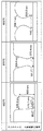
続いて、上記効果が得られていることについて、実験結果を参照して説明する。実験では、試料として、図4に示すように、SiCに代えてSi基板50を用い、Si基板50上にゲート絶縁膜7に相当するテトラエトキシシラン(以下、TEOS(Tetra Ethyl Ortho Silicateの略)という)膜51を形成し、その上に層間絶縁膜10に相当するBPSG膜52を形成した。そして、H2アニールを行ってから、BPSG膜52に対してコンタクトホール10aに相当するコンタクトホール52aを形成した。コンタクトホール52aのパターンについては複数種類用意し、各パターンについてBPSG膜52をエッチングしてコンタクトホール52aを形成したときの形状を調べ、コンタクトホール52aの形状変動を調べた。
Subsequently, the fact that the above effect is obtained will be described with reference to the experimental results. In the experiment, as shown in FIG. 4, a
具体的には、図5(a)〜(c)に示すように、複数の正方形のものをドット状に配置したパターン1、長方形の短ライン状のものを配列させたパターン2、もしくは、ライン状のものを並べたパターン3を用いて実験を行った。図5(a)〜(c)におけるX方向が図1の左右方向に相当しており、図5(a)、(b)に示すパターン1およびパターン2では、図1の断面において複数個並べられるようにコンタクトホール52aが配置される。コンタクトホール52aについては、図1のSiC半導体装置に適用される際には、少なくとも1つがn+型ソース領域4とコンタクト領域3aを露出させるように形成される。ここでは、パターン1ではコンタクトホール52aの各辺の長さa1を0.45μmとした。パターン2では、短辺a2を0.45μm、長辺b2を2.2μmとした。パターン3では、短辺a3を0.45μm、長辺b3を2000μmとした。そして、H2アニールの温度を800℃、870℃、930℃と変え、エッチング時間については223秒で統一してコンタクトホール52aの側壁の形状変動、つまり層間絶縁膜10の底面とコンタクトホール10aの側面との成す角度(以下、側壁角という)について調べた。
Specifically, as shown in FIGS. 5A to 5C, a
まず、図6(a)に示すように、パターン1については、H2アニールの温度を930℃とした場合、エッチング時間が短かったために底部にエッチング残りがあったが、側壁角は86.2°となっていた。さらに、側壁はほぼ直線状になっていて、切り立った状態となっていた。これに対して、H2アニールの温度を800℃または870℃とした場合、コンタクトホール52aの側壁角が115°または101.7°となっていた。より詳しくは、底部から入口側にかけて一旦は開口断面積が徐々に広がる順テーパ状となるが、さらに入口側になると徐々に狭まるような逆テーパ状となる。このため、側壁角が90°を超えてしまう。さらに入口側になると今度は開口断面積が徐々に広がる順テーパ状となるが、底部側において逆テーパ状となる部分が存在するため、好ましいトレンチ形状にはならなかった。
First, as shown in FIG. 6A, for
また、図6(b)に示すように、パターン2については、H2アニールの温度を930℃とした場合、エッチング時間が短かったために底部にエッチング残りがあったが、側壁角は87.8°となっていた。さらに、側壁はほぼ直線状になっていて、切り立った状態となっていた。これに対して、H2アニールの温度を870℃とした場合、コンタクトホール52aの側壁角が110°となっていた。より詳しくは、底部から入口側にかけて一旦は開口断面積が徐々に広がる順テーパ状となるが、さらに入口側になると徐々に狭まるような逆テーパ状となる。このため、側壁角が90°を超えてしまう。さらに入口側になると今度は開口断面積が徐々に広がる順テーパ状となるが、底部側において逆テーパ状となる部分が存在するため、好ましいトレンチ形状にはならなかった。また、H2アニールの温度を800℃とした場合、コンタクトホール52aの側壁角が88.5°となっていたが、入口側では底部側よりも開口断面積が広がっており、側壁は角部が丸みを帯びていて切り立った状態にはなっていなかった。
Further, as shown in FIG. 6 (b), for
さらに、図6(c)に示すように、パターン3については、H2アニールの温度を930℃または870℃とした場合、側壁角は86.6°または89.5°となっていた。さらに、側壁はほぼ直線状になっていて、切り立った状態となっていた。これに対して、H2アニールの温度を800℃とした場合、コンタクトホール52aの側壁角が90°となっていたが、入口側では底部側よりも開口断面積が広がっており、側壁は角部が丸みを帯びていて切り立った状態にはなっていなかった。
Further, as shown in FIG. 6 (c), for
ここで、層間絶縁膜10を固くすることによって応力の影響を抑制できるようにするには、側壁角が90°に近いこと、具体的には85°以上であることが好ましく、側壁が直線状に近く切り立った状態になっていることが条件となる。
Here, in order to suppress the influence of stress by hardening the interlayer insulating
これらの観点から、パターン1〜3の各温度でのコンタクトホール52aの側壁の形状変動を確認すると、パターン1〜3それぞれについて、コンタクトホール52aの側壁の形状変動から応力に対する耐性を有しているか否かが分かる。図7は、その結果をまとめた図表である。この図表に示されるように、パターン1、2では、H2アニールの温度を930℃とした場合には耐性有りでOK、870℃または800℃とした場合には耐性不十分でNGとなった。また、パターン3では、H2アニールの温度を930℃または870℃とした場合には耐性有りでOK、800℃とした場合には耐性不十分でNGとなった。
From these viewpoints, when the shape change of the side wall of the
このように、コンタクトホール10aの形状を変えたり、H2アニールの温度を変えたりした実験によれば、次のことが言える。まず、コンタクトホール10aを複数の正方形のものをドット状に配置したパターン1の場合、H2アニールの温度を930℃以上とすることで、応力に対する耐性を備えることが可能となる。また、コンタクトホール10aを長方形の短ライン状のものを配列させたパターン2の場合も、H2アニールの温度を930℃以上とすることで、応力に対する耐性を備えることが可能となる。さらに、コンタクトホール10aをライン状のものを並べたパターン3、H2アニールの温度を870℃以上とすることで、応力に対する耐性を備えることが可能となる。
According to the experiment in which the shape of the
なお、ここではパターン1〜3において、各辺の長さの一例を挙げて実験結果を示したが、ここで示した長さ以外であっても、同様の結果が得られた。実験結果からは、例えばパターン1の各辺の長さa1やパターン2、3の短辺の長さa2、a3が0.3〜0.6μmの範囲においては、上記と同様の結果が得られる。
Here, in
また、本実施形態のように、N2アニールによるリフローを行って層間絶縁膜10を流動させたのちに、H2アニールを行って層間絶縁膜10の緻密化を行った場合の各部の水素濃度もしくは不純物濃度について確認した。図8、図9および図10を参照して、層間絶縁膜10の緻密化と各部の水素濃度もしくは不純物濃度との関係について説明する。
Further, as in the present embodiment, the hydrogen concentration of each part is obtained when the
ここでも、実験用の試料として、図4の試料、すなわちSi基板50上にTEOS膜51を形成し、その上にBPSG膜52を形成したものを用い、N2アニールによるリフローやH2アニールを行った。そして、層間絶縁膜10としてBPSG膜を成膜しただけの状態、N2アニールによるリフローを行っただけの状態、および、リフロー後に温度を変えてH2アニールを行った場合、それぞれの場合について、水素濃度分布や不純物濃度分布を調べた。図8は、そのうちの水素濃度分布の測定結果を示してある。また、図9および図10は、それぞれ、リン濃度分布とボロン濃度分布の測定結果を示してある。
Again, as an experimental sample, a sample of FIG. 4, that is, a
図8を確認すると、リフロー前の状態では、まだリフローによる水素抜けが生じていないことから、BPSG膜52中の水素濃度が高くなっている。一方、リフローを行うと、水素抜けによって水素濃度が1×1020cm-3以下まで大幅に低下する。この状態では、BPSG膜52は緻密ではない状態、つまり柔らかい状態となっていて、応力の影響を抑制することができない。しかしながら、その後にH2アニールを行うと、水素濃度が増加し、1×1020cm-3以上になる。特に、870℃以上の温度、ここでは870℃および930℃の場合には、BPSG膜52の厚み方向のほぼ全域において水素濃度が1×1020cm-3以上になる。
As shown in FIG. 8, in the state before the reflow, the hydrogen concentration in the
このように、水素濃度が1×1020cm-3以上となるようにすると、BPSG膜52内においてSiO2になり切れていないSiやSi−Oと水素との結合力によって、BPSG膜52を緻密な状態にでき、応力の影響を抑制することが可能となる。
In this way, when the hydrogen concentration is set to 1 × 10 20 cm -3 or more, the
図9を確認すると、リフロー前の状態では、リン濃度が一定の状態となっている。この状態は、リンについて言えば、SiO2になり切れていないSiやSi−Oとリンとが結び付いて、BPSG膜52の結合力を高めることが可能な状態と言える。これに対して、リフローのみを行った場合や、リフロー後にH2アニールを行った場合には、TEOS膜51との境界位置においてリン濃度が低下しているものの、全域においてリン濃度が2wt%以上となっていた。さらに、H2アニールを930℃で行った場合には、BPSG膜52のうちのTEOS膜51の近傍において、極大値を有するようにリン濃度が高くなっていた。
When FIG. 9 is confirmed, the phosphorus concentration is constant in the state before the reflow. Speaking of phosphorus, this state can be said to be a state in which Si or Si—O that has not become SiO 2 can be combined with phosphorus to enhance the binding force of the
このように、H2アニールを行った後でもリン濃度を2wt%以上にできることから、SiO2になり切れていないSiやSi−Oとリンとが結び付いて、BPSG膜52の結合力を高めることが可能となる。特に、H2アニールを930℃で行った場合には、極大値において5wt%のリン濃度となっており、特にBPSG膜52を緻密なものにすることができる。したがって、H2アニールを行うこと、特に930℃以上で行うことで、BPSG膜52の緻密化を行うことが可能となり、応力の影響をより抑制することが可能になる。
In this way, since the phosphorus concentration can be increased to 2 wt% or more even after H 2 annealing, Si or Si—O that has not become SiO 2 is bound to phosphorus, and the binding force of the
図10を確認すると、リフロー前の状態では、ボロン濃度が一定の状態となっている。この状態は、ボロンに関しても、SiO2になり切れていないSiやSi−Oとボロンとが結び付いて、BPSG膜52の結合力を高めることが可能な状態と言える。これに対して、リフローのみを行った場合や、リフロー後にH2アニールを行った場合には、TEOS膜51との境界位置においてボロン濃度が低下しているものの、全域においてボロン濃度が2wt%以上となっていた。
When FIG. 10 is confirmed, the boron concentration is constant in the state before the reflow. In this state, it can be said that the bonding force of the
このように、H2アニールを行った後でもボロン濃度を2wt%以上にできることから、SiO2になり切れていないSiやSi−Oとボロンとが結び付いて、BPSG膜52の結合力を高めることが可能となる。したがって、H2アニールを行ってもボロン濃度を維持でき、BPSG膜52の緻密化を行えるため、応力の影響をより抑制することが可能になる。
In this way, since the boron concentration can be increased to 2 wt% or more even after H 2 annealing, Si and Si—O that have not completely become SiO 2 are combined with boron to enhance the binding force of the
さらに、本実施形態の場合、ゲート絶縁膜7が層間絶縁膜10の下地絶縁膜として残っていることから、上記実験で用いた試料のTEOS膜51がBPSG膜52の下地絶縁膜として残っているのと同様の構造となる。
Further, in the case of the present embodiment, since the
このTEOS膜51について見てみると、図8に示すように、水素濃度についてはBPSG膜52中の水素濃度よりも低く、1×1020cm-3未満、ここでは1×1019cm-3以下になっている。そして、TEOS膜51とBPSG膜52との界面において、TEOS膜51およびBPSG膜52の双方を含めた膜内における水素濃度が極大値となっている。これは、TEOS膜51がストッパーとなってBPSG膜52からの水素の拡散が抑制されていることを示している。このように、TEOS膜51、換言すればSiC半導体装置におけるゲート絶縁膜7が水素の拡散を止めるストッパーとして機能することで層間絶縁膜10への水素の充填が確実に行われるようにすることができる。
Looking at the
また、膜同士の界面では未結合手が多く存在しており、水素が未結合手と結合し易い状況となっている。このため、TEOS膜51とBPSG膜52との界面において水素濃度が極大値となるようにすると、界面に存在する未結合手が水素と結合するようにできる。このため、BPSG膜52の下地となるTEOS膜、換言すれば層間絶縁膜10の下地となるゲート絶縁膜7を強固な膜にすることが可能となり、より応力の影響によるクラックの発生などを抑制することが可能となる。
In addition, there are many unbonded hands at the interface between the membranes, and hydrogen is likely to bond with the unbonded hands. Therefore, when the hydrogen concentration is set to the maximum value at the interface between the
(第2実施形態)
第2実施形態について説明する。本実施形態は、第1実施形態に対してH2アニールの工程順序を変更したものであり、その他については第1実施形態と同様であるため、第1実施形態と異なる部分についてのみ説明する。
(Second Embodiment)
The second embodiment will be described. Since this embodiment is the same as the first embodiment in that the process order of H 2 annealing is changed from that of the first embodiment, only the parts different from the first embodiment will be described.
上記第1実施形態では、(1)の工程として、層間絶縁膜10を形成後、コンタクトホール10aの形成前に、層間絶縁膜10の緻密化処理としてH2アニールを行った。これに対して、本実施形態では、(1)の工程におけるコンタクトホール10aの形成後、かつ、(2)の工程における金属シリサイド9aの形成前に、層間絶縁膜10の緻密化処理としてH2アニールを行う。
In the first embodiment, as the step (1), H 2 annealing was performed as a densification treatment of the
上記したように、層間絶縁膜10に形成されるコンタクトホール10aの側壁の角部が丸まってしまうのは、高温処理が実施されるためである。このため、高温処理が行われる工程の前に、層間絶縁膜10の緻密化処理としてH2アニールを行えば、コンタクトホール10aの側壁の角部が丸まることを抑制できる。したがって、コンタクトホール10aの形成後、かつ、金属シリサイド9aの形成前に、層間絶縁膜10の緻密化処理としてH2アニールを行うようにしても、第1実施形態と同様の効果を奏することができる。
As described above, the corners of the side wall of the
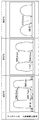
具体的に、本実施形態のような製造順序を適用しても、第1実施形態と同様の効果が得られていることについて、実験結果を参照して説明する。実験の方法については、第1実施形態と同様の手法を採用としており、図4に示したようなSi基板50上にTEOS膜51とBPSG膜52を形成した試料を用いた。そして、BPSG膜52に対して、図5(a)〜(c)に示すパターン1〜3の形状のコンタクトホール52aを形成し、コンタクトホール52aの形状変動を調べた。
Specifically, it will be described with reference to the experimental results that the same effect as that of the first embodiment is obtained even if the production sequence as in the present embodiment is applied. As the method of the experiment, the same method as in the first embodiment was adopted, and a sample in which the
まず、図11(a)に示すように、パターン1については、H2アニールの温度を930℃または870℃とした場合、側壁角はそれぞれ87.2°、86.6°となっていた。さらに、側壁はほぼ直線状になっていて、切り立った状態となっていた。これに対して、H2アニールの温度を800℃とした場合、コンタクトホール52aの側壁角が89.5°となっていたが、底部から入口側にかけて開口断面積が徐々に広がったのち、一旦狭まるような逆テーパ状となっていた。すなわち、側壁は全域で順テーパ状とはなっておらず、切り立った状態にはなっていなかった。
First, as shown in FIG. 11A, for
また、図11(b)に示すように、パターン2については、H2アニールの温度を930℃または870℃とした場合、側壁角はそれぞれ89.4°、88.2°となっていた。さらに、側壁はほぼ直線状になっていて、切り立った状態となっていた。これに対して、H2アニールの温度を800℃とした場合、コンタクトホール52aの側壁角が89.5°となっていたが、底部から入口側にかけて開口断面積が徐々に広がったのち、一旦狭まるような逆テーパ状となっていた。すなわち、側壁は全域で順テーパ状とはなっておらず、切り立った状態にはなっていなかった。
Further, as shown in FIG. 11B, for the
さらに、図11(c)に示すように、パターン3については、H2アニールの温度を930℃または870℃とした場合、側壁角は85.8または86.1°となっていた。さらに、側壁はほぼ直線状になっていて、切り立った状態となっていた。これに対して、H2アニールの温度を800℃とした場合、コンタクトホール52aの側壁角が84.8°となっていたが、入口側では底部側よりも開口断面積が広がっており、側壁は角部が丸みを帯びていて切り立った状態にはなっていなかった。
Further, as shown in FIG. 11 (c), for
上記したように、層間絶縁膜10を固くすることによって応力の影響を抑制できるようにするには、側壁角が90°に近いこと、具体的には85°以上であることが好ましく、側壁が直線状に近く切り立った状態になっていることが条件となる。
As described above, in order to suppress the influence of stress by hardening the interlayer insulating
これらの観点から、パターン1〜3の各温度でのコンタクトホール52aの側壁の形状変動を確認すると、パターン1〜3それぞれについて、コンタクトホール52aの側壁の形状変動から応力に対する耐性を有しているか否かが分かる。図12は、その結果をまとめた図表である。この図表に示されるように、パターン1〜3のいずれの場合も、H2アニールの温度を930℃、870℃とした場合には耐性有りでOK、800℃とした場合には耐性不十分でNGとなった。
From these viewpoints, when the shape change of the side wall of the
このように、コンタクトホール10aの形成後、かつ、金属シリサイド9aの形成前に、層間絶縁膜10の緻密化処理としてH2アニールを行うようにしても、第1実施形態と同様の効果を奏することができる。特に、パターン1、2については、930℃以上としなくても、870℃以上とすることで第1実施形態と同様の効果を奏することが可能となる。
As described above, even if the H 2 annealing is performed as the densification treatment of the
なお、ここでもパターン1〜3において、各辺の長さの一例を挙げて実験結果を示したが、ここで示した長さ以外であっても、同様の結果が得られた。実験結果からは、例えばパターン1の各辺の長さa1やパターン2、3の短辺の長さa2、a3が0.3〜0.6μmの範囲においては、上記と同様の結果が得られている。
In addition, although the experimental results were shown by giving an example of the length of each side in
(他の実施形態)
本発明は上記した実施形態に限定されるものではなく、特許請求の範囲に記載した範囲内において適宜変更が可能である。
(Other embodiments)
The present invention is not limited to the above-described embodiment, and can be appropriately modified within the scope of the claims.
例えば、上記実施形態では、SiC半導体装置を例に挙げて説明したが、その他の半導体材料、すなわちSiや化合物半導体を用いた半導体装置に対しても、本発明を適用することができる。 For example, in the above embodiment, the SiC semiconductor device has been described as an example, but the present invention can also be applied to other semiconductor materials, that is, semiconductor devices using Si or compound semiconductors.
また、応力の影響が特に顕著に現れるのは、第1、第2実施形態で説明したようなゲート絶縁膜7を備えるMOS構造の半導体素子を有する半導体装置であるが、応力の影響はMOS構造の半導体素子に限らず発生する。このため、第1、第2実施形態で説明したMOSFETに加えて、それ以外のMOS構造を有する半導体素子や、MOS構造以外の半導体素子を有する半導体装置に対しても、本発明を適用することができる。
Further, the influence of stress is particularly remarkable in a semiconductor device having a semiconductor element having a MOS structure provided with the
例えば、上記第1実施形態等では、第1導電型をn型、第2導電型をp型としたnチャネルタイプのMOSFETを例に挙げて説明したが、各構成要素の導電型を反転させたpチャネルタイプのMOSFETとしても良い。また、半導体素子としてMOSFETに加えて、同様の構造のIGBTに対しても本発明を適用することができる。IGBTは、上記各実施形態に対してn+型基板1の導電型をn型からp型に変更するだけであり、その他の構造や製造方法に関しては上記各実施形態と同様である。さらに、縦型のMOSFETとしてトレンチゲート構造のものを例に挙げて説明したが、トレンチゲート構造のものに限らず、プレーナ型のものであっても良い。また、MOS構造の半導体素子以外の半導体素子として、例えばショットキーバリアダイオードなどを有する半導体装置に対して本発明を適用することもできる。 For example, in the first embodiment and the like, an n-channel type MOSFET in which the first conductive type is n-type and the second conductive type is p-type has been described as an example, but the conductive type of each component is inverted. It may be a p-channel type MOSFET. Further, in addition to the MOSFET as a semiconductor element, the present invention can be applied to an IGBT having a similar structure. The IGBT only changes the conductive type of the n + type substrate 1 from the n type to the p type for each of the above embodiments, and is the same as each of the above embodiments in terms of other structures and manufacturing methods. Further, although the vertical MOSFET having a trench gate structure has been described as an example, the MOSFET is not limited to the trench gate structure and may be a planar type MOSFET. Further, the present invention can be applied to a semiconductor device having, for example, a Schottky barrier diode as a semiconductor element other than the semiconductor element having a MOS structure.
さらに、上記第1、第2実施形態で説明したSiC半導体装置の製造方法も一例を示したに過ぎず、必要に応じて工程を追加したり、削除したり、他の工程に変更することもできる。例えば、金属シリサイド9aの形成工程については、コンタクト抵抗低減のために実施することが好ましいが、この工程を削減しても良い。また、この金属シリサイド9aの形成工程を高温処理が行われる工程の一例として示したが、他の高温処理が行われる工程についても、応力発生要因になり得ることから、金属シリサイド9aの形成工程を行わなかったとしても、層間絶縁膜10の緻密化処理を行うことによる効果はある。
Further, the manufacturing method of the SiC semiconductor device described in the first and second embodiments is only an example, and steps may be added, deleted, or changed to other steps as necessary. it can. For example, the step of forming the
また、図1に示した例では、n+型ソース領域4がイオン注入によって形成される場合を想定しているが、n+型ソース領域4をエピタキシャル成長によって形成することもできる。
Further, in the example shown in FIG. 1, it is assumed that the n +
3 p型ベース領域
4 n+型ソース領域
9 ソース電極
9a 金属シリサイド
9b、31a バリアメタル
9c、31b Wプラグ
9d、31c Al−Si層
10 層間絶縁膜
10a、10b コンタクトホール
3 p-type base region 4 n + -type source region 9
Claims (13)
前記半導体の上に形成され、前記半導体素子に繋がるコンタクトホール(10a)を有し、リンとボロンの少なくとも一方を含んで構成された層間絶縁膜(10)と、
前記層間絶縁膜の上に形成され、前記コンタクトホールを通じて前記半導体素子と接続される金属電極(9d)と、を有し、
前記層間絶縁膜内に水素が充填されており、
さらに、前記層間絶縁膜にはリンが含まれており、該層間絶縁膜内においてリン濃度分布の極大値がある半導体装置。 Semiconductors (1 to 5) on which semiconductor elements are formed and
An interlayer insulating film (10) formed on the semiconductor, having a contact hole (10a) connected to the semiconductor element, and containing at least one of phosphorus and boron.
It has a metal electrode (9d) formed on the interlayer insulating film and connected to the semiconductor element through the contact hole.
Hydrogen is filled in the interlayer insulating film, and the interlayer insulating film is filled with hydrogen.
Further, a semiconductor device in which phosphorus is contained in the interlayer insulating film and the phosphorus concentration distribution has a maximum value in the interlayer insulating film.
前記半導体の上に形成され、前記半導体素子に繋がるコンタクトホール(10a)を有し、リンとボロンの少なくとも一方を含んで構成された層間絶縁膜(10)と、
前記層間絶縁膜の上に形成され、前記コンタクトホールを通じて前記半導体素子と接続される金属電極(9d)と、を有し、
前記層間絶縁膜内に水素が充填されており、
前記層間絶縁膜内における水素濃度が1×1020cm−3以上であって、
前記層間絶縁膜にはリンが含まれており、該層間絶縁膜内においてリン濃度分布の極大値がある半導体装置。 Semiconductors (1 to 5) on which semiconductor elements are formed and
An interlayer insulating film (10) formed on the semiconductor, having a contact hole (10a) connected to the semiconductor element, and containing at least one of phosphorus and boron.
It has a metal electrode (9d) formed on the interlayer insulating film and connected to the semiconductor element through the contact hole.
Hydrogen is filled in the interlayer insulating film, and the interlayer insulating film is filled with hydrogen.
Hydrogen concentration der less than 1 × 10 20 cm -3 in the interlayer insulating film,
A semiconductor device in which phosphorus is contained in the interlayer insulating film and the phosphorus concentration distribution has a maximum value in the interlayer insulating film .
前記層間絶縁膜は、前記段差も覆うように形成されている請求項1ないし7のいずれか1つに記載の半導体装置。 The semiconductor has a cell portion on which the semiconductor element is formed and an outer peripheral portion including a guard ring portion surrounding the cell portion, and a recess (20) is formed in the semiconductor in the guard ring portion. A step is formed between the cell portion and the guard ring portion.
The semiconductor device according to any one of claims 1 to 7 , wherein the interlayer insulating film is formed so as to cover the step.
前記半導体として、裏面側が第1導電型もしくは第2導電型の高濃度不純物層(1)とされていると共に表面側が前記高濃度不純物層よりも低不純物濃度とされた第1導電型のドリフト層(2)とされ、炭化珪素にて構成された半導体基板(1、2)と、前記ドリフト層の上に形成された第2導電型の炭化珪素からなるベース領域(3)と、前記ベース領域の上に形成され、前記ドリフト層よりも高不純物濃度の第1導電型の炭化珪素で構成されたソース領域(4)と、を有し、
さらに、前記ソース領域の表面から前記ベース領域よりも深くまで形成されたゲートトレンチ(6)内に形成され、該ゲートトレンチの内壁面に形成されたゲート絶縁膜(7)と、前記ゲート絶縁膜の上に形成されたゲート電極(8)と、を有して構成されたトレンチゲート構造と、
前記ソース領域および前記ベース領域に接続された第1電極(9)と、
前記高濃度不純物層に接続された第2電極(11)と、を有しており、
前記ゲート絶縁膜は、前記下地絶縁膜を構成しており、
前記金属電極は、前記第1電極に含まれている請求項9ないし11のいずれか1つに記載の半導体装置。 The semiconductor element is
As the semiconductor, the back surface side is a first conductive type or second conductive type high concentration impurity layer (1), and the front surface side is a first conductive type drift layer having a lower impurity concentration than the high concentration impurity layer. (2), a base region (3) made of a semiconductor substrate (1, 2) made of silicon carbide, a second conductive type silicon carbide formed on the drift layer, and the base region. It has a source region (4) formed on the above and composed of first conductive type silicon carbide having a higher impurity concentration than the drift layer.
Further, a gate insulating film (7) formed in the gate trench (6) formed from the surface of the source region to a depth deeper than the base region and formed on the inner wall surface of the gate trench, and the gate insulating film. A trench gate structure configured with a gate electrode (8) formed on top of the gate electrode (8).
The first electrode (9) connected to the source region and the base region,
It has a second electrode (11) connected to the high-concentration impurity layer, and has.
The gate insulating film constitutes the underlying insulating film.
The semiconductor device according to any one of claims 9 to 11 , wherein the metal electrode is included in the first electrode.
前記半導体の上に形成され、前記半導体素子に繋がるコンタクトホール(10a)を有し、リンとボロンの少なくとも一方を含んで構成された層間絶縁膜(10)と、
前記層間絶縁膜の上に形成され、前記コンタクトホールを通じて前記半導体素子と接続される金属電極(9d)と、を有し、
前記半導体のうち前記半導体素子が形成されたセル部と、該セル部を囲むガードリング部を含む外周部とを有し、前記ガードリング部において前記半導体に凹部(20)が形成されていて、前記セル部と前記ガードリング部との間において段差が構成されており、
前記層間絶縁膜が前記段差も覆うように形成される半導体装置の製造方法であって、
前記凹部が形成されることで前記段差が構成された前記半導体の上に前記層間絶縁膜を成膜することと、
リフローを行うことで、前記層間絶縁膜を流動させ、前記段差を所定の膜厚の前記層間絶縁膜で覆うことと、
前記段差を所定の膜厚の前記層間絶縁膜で覆うことの後に、前記コンタクトホールを形成することと、
前記コンタクトホールを形成することの後に、水素アニールを870℃以上で行うことで、前記層間絶縁膜内に水素を充填して該層間絶縁膜の緻密化処理を行うことと、を含んでいる半導体装置の製造方法。 Semiconductors (1 to 5) on which semiconductor elements are formed and
An interlayer insulating film (10) formed on the semiconductor, having a contact hole (10a) connected to the semiconductor element, and containing at least one of phosphorus and boron.
It has a metal electrode (9d) formed on the interlayer insulating film and connected to the semiconductor element through the contact hole.
The semiconductor has a cell portion on which the semiconductor element is formed and an outer peripheral portion including a guard ring portion surrounding the cell portion, and a recess (20) is formed in the semiconductor in the guard ring portion. A step is formed between the cell portion and the guard ring portion.
A method for manufacturing a semiconductor device in which the interlayer insulating film is formed so as to cover the step.
The interlayer insulating film is formed on the semiconductor in which the step is formed by forming the recess.
By performing the reflow, the interlayer insulating film is made to flow, and the step is covered with the interlayer insulating film having a predetermined film thickness.
After covering the step with the interlayer insulating film having a predetermined film thickness, the contact hole is formed.
A semiconductor including that, after forming the contact hole, hydrogen annealing is performed at 870 ° C. or higher to fill the interlayer insulating film with hydrogen and perform a densification treatment of the interlayer insulating film. How to manufacture the device.
Priority Applications (4)
| Application Number | Priority Date | Filing Date | Title |
|---|---|---|---|
| JP2017006002A JP6828449B2 (en) | 2017-01-17 | 2017-01-17 | Semiconductor devices and their manufacturing methods |
| CN201880006937.6A CN110235229B (en) | 2017-01-17 | 2018-01-17 | Semiconductor device and method for manufacturing the same |
| PCT/JP2018/001260 WO2018135541A1 (en) | 2017-01-17 | 2018-01-17 | Semiconductor device and method for manufacturing same |
| US16/511,345 US10923395B2 (en) | 2017-01-17 | 2019-07-15 | Semiconductor device and manufacturing method of semiconductor device |
Applications Claiming Priority (1)
| Application Number | Priority Date | Filing Date | Title |
|---|---|---|---|
| JP2017006002A JP6828449B2 (en) | 2017-01-17 | 2017-01-17 | Semiconductor devices and their manufacturing methods |
Publications (3)
| Publication Number | Publication Date |
|---|---|
| JP2018117016A JP2018117016A (en) | 2018-07-26 |
| JP2018117016A5 JP2018117016A5 (en) | 2019-04-25 |
| JP6828449B2 true JP6828449B2 (en) | 2021-02-10 |
Family
ID=62908552
Family Applications (1)
| Application Number | Title | Priority Date | Filing Date |
|---|---|---|---|
| JP2017006002A Active JP6828449B2 (en) | 2017-01-17 | 2017-01-17 | Semiconductor devices and their manufacturing methods |
Country Status (4)
| Country | Link |
|---|---|
| US (1) | US10923395B2 (en) |
| JP (1) | JP6828449B2 (en) |
| CN (1) | CN110235229B (en) |
| WO (1) | WO2018135541A1 (en) |
Families Citing this family (15)
| Publication number | Priority date | Publication date | Assignee | Title |
|---|---|---|---|---|
| WO2019069580A1 (en) * | 2017-10-05 | 2019-04-11 | 富士電機株式会社 | Semiconductor device |
| DE112019003465T5 (en) * | 2018-08-07 | 2021-03-25 | Rohm Co., Ltd. | SiC SEMICONDUCTOR DEVICE |
| DE202019005382U1 (en) | 2018-08-10 | 2020-06-17 | Rohm Co., Ltd. | SiC semiconductor device |
| JP7188230B2 (en) * | 2019-03-28 | 2022-12-13 | 株式会社デンソー | semiconductor equipment |
| JP7443673B2 (en) * | 2019-04-15 | 2024-03-06 | 富士電機株式会社 | silicon carbide semiconductor device |
| JP7081564B2 (en) * | 2019-04-24 | 2022-06-07 | 株式会社デンソー | Semiconductor devices and their manufacturing methods |
| JP7472435B2 (en) * | 2019-05-13 | 2024-04-23 | 富士電機株式会社 | Semiconductor module manufacturing method |
| JP7476502B2 (en) * | 2019-09-06 | 2024-05-01 | 富士電機株式会社 | Semiconductor Device |
| JP7404722B2 (en) * | 2019-09-06 | 2023-12-26 | 富士電機株式会社 | semiconductor equipment |
| JP7129397B2 (en) * | 2019-12-06 | 2022-09-01 | ローム株式会社 | SiC semiconductor device |
| JP7129436B2 (en) * | 2020-02-17 | 2022-09-01 | ローム株式会社 | SiC semiconductor device |
| JP7129437B2 (en) * | 2020-02-17 | 2022-09-01 | ローム株式会社 | SiC semiconductor device |
| JP2022168904A (en) * | 2021-04-27 | 2022-11-09 | 富士電機株式会社 | Silicon carbide semiconductor device and method for manufacturing silicon carbide semiconductor device |
| CN114583013A (en) * | 2022-03-10 | 2022-06-03 | 常州时创能源股份有限公司 | BSG removing method |
| JP2024120450A (en) | 2023-02-24 | 2024-09-05 | 三菱電機株式会社 | Semiconductor device and method for manufacturing the same |
Family Cites Families (21)
| Publication number | Priority date | Publication date | Assignee | Title |
|---|---|---|---|---|
| JPH0456222A (en) * | 1990-06-25 | 1992-02-24 | Matsushita Electron Corp | Manufacture of semiconductor device |
| JPH0582781A (en) * | 1991-09-24 | 1993-04-02 | Nec Yamagata Ltd | Semiconductor integrated circuit device |
| JPH06177129A (en) * | 1992-12-09 | 1994-06-24 | Oki Electric Ind Co Ltd | Fabrication of semiconductor device |
| JP2757782B2 (en) * | 1994-06-30 | 1998-05-25 | 日本電気株式会社 | Method for manufacturing semiconductor device |
| JP3543504B2 (en) * | 1996-08-06 | 2004-07-14 | ソニー株式会社 | Method for manufacturing semiconductor device |
| JP2002134607A (en) * | 2000-10-20 | 2002-05-10 | Hitachi Ltd | Method of manufacturing semiconductor integrated circuit device |
| CN101088155A (en) * | 2004-10-25 | 2007-12-12 | 斯班逊有限公司 | Semiconductor device and its manufacturing method |
| JP2007096263A (en) | 2005-08-31 | 2007-04-12 | Denso Corp | SiC SEMICONDUCTOR DEVICE AND METHOD OF MANUFACTURING SAME |
| KR100872981B1 (en) * | 2007-07-19 | 2008-12-08 | 주식회사 동부하이텍 | Method of fabricating semiconductor |
| EP2091083A3 (en) | 2008-02-13 | 2009-10-14 | Denso Corporation | Silicon carbide semiconductor device including a deep layer |
| JP2010165778A (en) * | 2009-01-14 | 2010-07-29 | Sharp Corp | Method of manufacturing semiconductor device |
| JP5813303B2 (en) | 2009-11-20 | 2015-11-17 | 株式会社日立国際電気 | Semiconductor device manufacturing method, substrate processing method, and substrate processing apparatus |
| JP5770892B2 (en) * | 2009-11-20 | 2015-08-26 | 株式会社日立国際電気 | Semiconductor device manufacturing method, substrate processing method, and substrate processing apparatus |
| KR101995682B1 (en) * | 2011-03-18 | 2019-07-02 | 가부시키가이샤 한도오따이 에네루기 켄큐쇼 | Oxide semiconductor film, semiconductor device, and manufacturing method of semiconductor device |
| JP2013041919A (en) | 2011-08-12 | 2013-02-28 | Renesas Electronics Corp | Semiconductor device manufacturing method |
| JP6245723B2 (en) | 2012-04-27 | 2017-12-13 | 富士電機株式会社 | Method for manufacturing silicon carbide semiconductor device |
| JP2014027076A (en) * | 2012-07-26 | 2014-02-06 | Renesas Electronics Corp | Semiconductor device |
| JP6160477B2 (en) * | 2013-12-25 | 2017-07-12 | トヨタ自動車株式会社 | Semiconductor device |
| CN106463504B (en) | 2014-11-17 | 2019-11-29 | 富士电机株式会社 | The manufacturing method of semiconductor device and semiconductor device |
| WO2016125490A1 (en) * | 2015-02-03 | 2016-08-11 | 富士電機株式会社 | Semiconductor device and method for manufacturing same |
| JP6409681B2 (en) * | 2015-05-29 | 2018-10-24 | 株式会社デンソー | Semiconductor device and manufacturing method thereof |
-
2017
- 2017-01-17 JP JP2017006002A patent/JP6828449B2/en active Active
-
2018
- 2018-01-17 WO PCT/JP2018/001260 patent/WO2018135541A1/en active Application Filing
- 2018-01-17 CN CN201880006937.6A patent/CN110235229B/en active Active
-
2019
- 2019-07-15 US US16/511,345 patent/US10923395B2/en active Active
Also Published As
| Publication number | Publication date |
|---|---|
| CN110235229B (en) | 2022-08-12 |
| US20190341308A1 (en) | 2019-11-07 |
| WO2018135541A1 (en) | 2018-07-26 |
| JP2018117016A (en) | 2018-07-26 |
| CN110235229A (en) | 2019-09-13 |
| US10923395B2 (en) | 2021-02-16 |
Similar Documents
| Publication | Publication Date | Title |
|---|---|---|
| JP6828449B2 (en) | Semiconductor devices and their manufacturing methods | |
| JP6341074B2 (en) | Manufacturing method of semiconductor device | |
| JP6354525B2 (en) | Method for manufacturing silicon carbide semiconductor device | |
| JP4913336B2 (en) | Semiconductor device | |
| CN106549003A (en) | Through substrate through vias structure and its manufacture method | |
| US10707343B2 (en) | Method of manufacturing semiconductor device and semiconductor device | |
| US10825909B2 (en) | Method of manufacturing semiconductor device and semiconductor device | |
| CN103151377A (en) | Lateral transistor component and method for producing same | |
| WO2015174197A1 (en) | Semiconductor device and method for manufacturing semiconductor device | |
| JP7369601B2 (en) | Semiconductor device and its manufacturing method | |
| JP2008182106A (en) | Semiconductor device | |
| US20160172301A1 (en) | Semiconductor device and manufacturing method therefor | |
| JP7069605B2 (en) | Manufacturing method of semiconductor device | |
| JP2010103208A (en) | Semiconductor device | |
| JP4860122B2 (en) | Manufacturing method of semiconductor device | |
| JP6750590B2 (en) | Silicon carbide semiconductor device | |
| US20160211349A1 (en) | Semiconductor device and a method for manufacturing a semiconductor device | |
| JP2002314081A (en) | Trench-gate type semiconductor device and its manufacturing method | |
| JP2013509729A (en) | Semiconductor element | |
| US20160163647A1 (en) | Semiconductor device and manufacturing method therefor | |
| CN105830203B (en) | Semiconductor device | |
| JP2013098228A (en) | Semiconductor device and manufacturing method thereof | |
| JPWO2017126084A1 (en) | Semiconductor device | |
| JP6623824B2 (en) | Semiconductor device and method of manufacturing the same | |
| JP2010027695A (en) | Semiconductor device, and manufacturing method therefor |
Legal Events
| Date | Code | Title | Description |
|---|---|---|---|
| A521 | Request for written amendment filed |
Free format text: JAPANESE INTERMEDIATE CODE: A523 Effective date: 20190315 |
|
| A621 | Written request for application examination |
Free format text: JAPANESE INTERMEDIATE CODE: A621 Effective date: 20190315 |
|
| A131 | Notification of reasons for refusal |
Free format text: JAPANESE INTERMEDIATE CODE: A131 Effective date: 20200526 |
|
| A521 | Request for written amendment filed |
Free format text: JAPANESE INTERMEDIATE CODE: A523 Effective date: 20200724 |
|
| A711 | Notification of change in applicant |
Free format text: JAPANESE INTERMEDIATE CODE: A711 Effective date: 20200807 |
|
| A521 | Request for written amendment filed |
Free format text: JAPANESE INTERMEDIATE CODE: A821 Effective date: 20200807 |
|
| TRDD | Decision of grant or rejection written | ||
| A01 | Written decision to grant a patent or to grant a registration (utility model) |
Free format text: JAPANESE INTERMEDIATE CODE: A01 Effective date: 20201222 |
|
| A61 | First payment of annual fees (during grant procedure) |
Free format text: JAPANESE INTERMEDIATE CODE: A61 Effective date: 20210104 |
|
| R150 | Certificate of patent or registration of utility model |
Ref document number: 6828449 Country of ref document: JP Free format text: JAPANESE INTERMEDIATE CODE: R150 |
|
| R250 | Receipt of annual fees |
Free format text: JAPANESE INTERMEDIATE CODE: R250 |