JP4860122B2 - Manufacturing method of semiconductor device - Google Patents
Manufacturing method of semiconductor device Download PDFInfo
- Publication number
- JP4860122B2 JP4860122B2 JP2004188290A JP2004188290A JP4860122B2 JP 4860122 B2 JP4860122 B2 JP 4860122B2 JP 2004188290 A JP2004188290 A JP 2004188290A JP 2004188290 A JP2004188290 A JP 2004188290A JP 4860122 B2 JP4860122 B2 JP 4860122B2
- Authority
- JP
- Japan
- Prior art keywords
- groove
- region
- film
- semiconductor layer
- conductive film
- Prior art date
- Legal status (The legal status is an assumption and is not a legal conclusion. Google has not performed a legal analysis and makes no representation as to the accuracy of the status listed.)
- Active
Links
- 239000004065 semiconductor Substances 0.000 title claims description 202
- 238000004519 manufacturing process Methods 0.000 title claims description 70
- 239000000758 substrate Substances 0.000 claims description 68
- 238000000034 method Methods 0.000 claims description 31
- 239000012535 impurity Substances 0.000 claims description 18
- 230000000149 penetrating effect Effects 0.000 claims description 9
- 238000000059 patterning Methods 0.000 claims description 8
- 238000005530 etching Methods 0.000 claims description 7
- 238000005229 chemical vapour deposition Methods 0.000 claims description 5
- VYPSYNLAJGMNEJ-UHFFFAOYSA-N Silicium dioxide Chemical compound O=[Si]=O VYPSYNLAJGMNEJ-UHFFFAOYSA-N 0.000 description 96
- 229910052814 silicon oxide Inorganic materials 0.000 description 96
- 239000005380 borophosphosilicate glass Substances 0.000 description 55
- 239000010410 layer Substances 0.000 description 38
- 230000015556 catabolic process Effects 0.000 description 17
- 239000011229 interlayer Substances 0.000 description 15
- 229910021421 monocrystalline silicon Inorganic materials 0.000 description 14
- 229910021420 polycrystalline silicon Inorganic materials 0.000 description 14
- 229920002120 photoresistant polymer Polymers 0.000 description 13
- 238000000605 extraction Methods 0.000 description 11
- 238000000206 photolithography Methods 0.000 description 11
- 238000010438 heat treatment Methods 0.000 description 7
- 230000003071 parasitic effect Effects 0.000 description 6
- XUIMIQQOPSSXEZ-UHFFFAOYSA-N Silicon Chemical compound [Si] XUIMIQQOPSSXEZ-UHFFFAOYSA-N 0.000 description 4
- 239000004020 conductor Substances 0.000 description 4
- 229910052710 silicon Inorganic materials 0.000 description 4
- 239000010703 silicon Substances 0.000 description 4
- ZOXJGFHDIHLPTG-UHFFFAOYSA-N Boron Chemical compound [B] ZOXJGFHDIHLPTG-UHFFFAOYSA-N 0.000 description 3
- 229910052581 Si3N4 Inorganic materials 0.000 description 3
- 229910052796 boron Inorganic materials 0.000 description 3
- 230000000694 effects Effects 0.000 description 3
- 239000010931 gold Substances 0.000 description 3
- PXHVJJICTQNCMI-UHFFFAOYSA-N nickel Substances [Ni] PXHVJJICTQNCMI-UHFFFAOYSA-N 0.000 description 3
- 230000003647 oxidation Effects 0.000 description 3
- 238000007254 oxidation reaction Methods 0.000 description 3
- 229920001721 polyimide Polymers 0.000 description 3
- 239000009719 polyimide resin Substances 0.000 description 3
- HQVNEWCFYHHQES-UHFFFAOYSA-N silicon nitride Chemical compound N12[Si]34N5[Si]62N3[Si]51N64 HQVNEWCFYHHQES-UHFFFAOYSA-N 0.000 description 3
- 238000004544 sputter deposition Methods 0.000 description 3
- OAICVXFJPJFONN-UHFFFAOYSA-N Phosphorus Chemical compound [P] OAICVXFJPJFONN-UHFFFAOYSA-N 0.000 description 2
- 230000004888 barrier function Effects 0.000 description 2
- 230000015572 biosynthetic process Effects 0.000 description 2
- 238000000151 deposition Methods 0.000 description 2
- 230000005669 field effect Effects 0.000 description 2
- 230000007257 malfunction Effects 0.000 description 2
- 239000002184 metal Substances 0.000 description 2
- 229910052751 metal Inorganic materials 0.000 description 2
- 229910052698 phosphorus Inorganic materials 0.000 description 2
- 239000011574 phosphorus Substances 0.000 description 2
- 230000001681 protective effect Effects 0.000 description 2
- 239000010936 titanium Substances 0.000 description 2
- RTAQQCXQSZGOHL-UHFFFAOYSA-N Titanium Chemical compound [Ti] RTAQQCXQSZGOHL-UHFFFAOYSA-N 0.000 description 1
- 230000004913 activation Effects 0.000 description 1
- 229910052782 aluminium Inorganic materials 0.000 description 1
- XAGFODPZIPBFFR-UHFFFAOYSA-N aluminium Chemical compound [Al] XAGFODPZIPBFFR-UHFFFAOYSA-N 0.000 description 1
- 238000006243 chemical reaction Methods 0.000 description 1
- 239000013078 crystal Substances 0.000 description 1
- 238000009792 diffusion process Methods 0.000 description 1
- OKZIUSOJQLYFSE-UHFFFAOYSA-N difluoroboron Chemical compound F[B]F OKZIUSOJQLYFSE-UHFFFAOYSA-N 0.000 description 1
- PCHJSUWPFVWCPO-UHFFFAOYSA-N gold Chemical compound [Au] PCHJSUWPFVWCPO-UHFFFAOYSA-N 0.000 description 1
- 229910052737 gold Inorganic materials 0.000 description 1
- 230000012447 hatching Effects 0.000 description 1
- 239000012212 insulator Substances 0.000 description 1
- 229910044991 metal oxide Inorganic materials 0.000 description 1
- 150000004706 metal oxides Chemical class 0.000 description 1
- 150000002739 metals Chemical class 0.000 description 1
- 238000012986 modification Methods 0.000 description 1
- 230000004048 modification Effects 0.000 description 1
- 229910052759 nickel Inorganic materials 0.000 description 1
- 230000001590 oxidative effect Effects 0.000 description 1
- 230000003252 repetitive effect Effects 0.000 description 1
- 239000011347 resin Substances 0.000 description 1
- 229920005989 resin Polymers 0.000 description 1
- 229910052719 titanium Inorganic materials 0.000 description 1
- MAKDTFFYCIMFQP-UHFFFAOYSA-N titanium tungsten Chemical compound [Ti].[W] MAKDTFFYCIMFQP-UHFFFAOYSA-N 0.000 description 1
Images


Classifications
-
- H—ELECTRICITY
- H01—ELECTRIC ELEMENTS
- H01L—SEMICONDUCTOR DEVICES NOT COVERED BY CLASS H10
- H01L29/00—Semiconductor devices adapted for rectifying, amplifying, oscillating or switching, or capacitors or resistors with at least one potential-jump barrier or surface barrier, e.g. PN junction depletion layer or carrier concentration layer; Details of semiconductor bodies or of electrodes thereof ; Multistep manufacturing processes therefor
- H01L29/66—Types of semiconductor device ; Multistep manufacturing processes therefor
- H01L29/68—Types of semiconductor device ; Multistep manufacturing processes therefor controllable by only the electric current supplied, or only the electric potential applied, to an electrode which does not carry the current to be rectified, amplified or switched
- H01L29/76—Unipolar devices, e.g. field effect transistors
- H01L29/772—Field effect transistors
- H01L29/78—Field effect transistors with field effect produced by an insulated gate
- H01L29/7801—DMOS transistors, i.e. MISFETs with a channel accommodating body or base region adjoining a drain drift region
- H01L29/7802—Vertical DMOS transistors, i.e. VDMOS transistors
- H01L29/7813—Vertical DMOS transistors, i.e. VDMOS transistors with trench gate electrode, e.g. UMOS transistors
-
- H—ELECTRICITY
- H01—ELECTRIC ELEMENTS
- H01L—SEMICONDUCTOR DEVICES NOT COVERED BY CLASS H10
- H01L29/00—Semiconductor devices adapted for rectifying, amplifying, oscillating or switching, or capacitors or resistors with at least one potential-jump barrier or surface barrier, e.g. PN junction depletion layer or carrier concentration layer; Details of semiconductor bodies or of electrodes thereof ; Multistep manufacturing processes therefor
- H01L29/40—Electrodes ; Multistep manufacturing processes therefor
- H01L29/402—Field plates
- H01L29/407—Recessed field plates, e.g. trench field plates, buried field plates
-
- H—ELECTRICITY
- H01—ELECTRIC ELEMENTS
- H01L—SEMICONDUCTOR DEVICES NOT COVERED BY CLASS H10
- H01L29/00—Semiconductor devices adapted for rectifying, amplifying, oscillating or switching, or capacitors or resistors with at least one potential-jump barrier or surface barrier, e.g. PN junction depletion layer or carrier concentration layer; Details of semiconductor bodies or of electrodes thereof ; Multistep manufacturing processes therefor
- H01L29/66—Types of semiconductor device ; Multistep manufacturing processes therefor
- H01L29/68—Types of semiconductor device ; Multistep manufacturing processes therefor controllable by only the electric current supplied, or only the electric potential applied, to an electrode which does not carry the current to be rectified, amplified or switched
- H01L29/76—Unipolar devices, e.g. field effect transistors
- H01L29/772—Field effect transistors
- H01L29/78—Field effect transistors with field effect produced by an insulated gate
- H01L29/7801—DMOS transistors, i.e. MISFETs with a channel accommodating body or base region adjoining a drain drift region
- H01L29/7802—Vertical DMOS transistors, i.e. VDMOS transistors
- H01L29/7811—Vertical DMOS transistors, i.e. VDMOS transistors with an edge termination structure
-
- H—ELECTRICITY
- H01—ELECTRIC ELEMENTS
- H01L—SEMICONDUCTOR DEVICES NOT COVERED BY CLASS H10
- H01L29/00—Semiconductor devices adapted for rectifying, amplifying, oscillating or switching, or capacitors or resistors with at least one potential-jump barrier or surface barrier, e.g. PN junction depletion layer or carrier concentration layer; Details of semiconductor bodies or of electrodes thereof ; Multistep manufacturing processes therefor
- H01L29/40—Electrodes ; Multistep manufacturing processes therefor
- H01L29/41—Electrodes ; Multistep manufacturing processes therefor characterised by their shape, relative sizes or dispositions
- H01L29/423—Electrodes ; Multistep manufacturing processes therefor characterised by their shape, relative sizes or dispositions not carrying the current to be rectified, amplified or switched
- H01L29/42312—Gate electrodes for field effect devices
- H01L29/42316—Gate electrodes for field effect devices for field-effect transistors
- H01L29/4232—Gate electrodes for field effect devices for field-effect transistors with insulated gate
- H01L29/42356—Disposition, e.g. buried gate electrode
- H01L29/4236—Disposition, e.g. buried gate electrode within a trench, e.g. trench gate electrode, groove gate electrode
-
- H—ELECTRICITY
- H01—ELECTRIC ELEMENTS
- H01L—SEMICONDUCTOR DEVICES NOT COVERED BY CLASS H10
- H01L29/00—Semiconductor devices adapted for rectifying, amplifying, oscillating or switching, or capacitors or resistors with at least one potential-jump barrier or surface barrier, e.g. PN junction depletion layer or carrier concentration layer; Details of semiconductor bodies or of electrodes thereof ; Multistep manufacturing processes therefor
- H01L29/40—Electrodes ; Multistep manufacturing processes therefor
- H01L29/41—Electrodes ; Multistep manufacturing processes therefor characterised by their shape, relative sizes or dispositions
- H01L29/423—Electrodes ; Multistep manufacturing processes therefor characterised by their shape, relative sizes or dispositions not carrying the current to be rectified, amplified or switched
- H01L29/42312—Gate electrodes for field effect devices
- H01L29/42316—Gate electrodes for field effect devices for field-effect transistors
- H01L29/4232—Gate electrodes for field effect devices for field-effect transistors with insulated gate
- H01L29/42372—Gate electrodes for field effect devices for field-effect transistors with insulated gate characterised by the conducting layer, e.g. the length, the sectional shape or the lay-out
- H01L29/4238—Gate electrodes for field effect devices for field-effect transistors with insulated gate characterised by the conducting layer, e.g. the length, the sectional shape or the lay-out characterised by the surface lay-out
-
- H—ELECTRICITY
- H01—ELECTRIC ELEMENTS
- H01L—SEMICONDUCTOR DEVICES NOT COVERED BY CLASS H10
- H01L2924/00—Indexing scheme for arrangements or methods for connecting or disconnecting semiconductor or solid-state bodies as covered by H01L24/00
- H01L2924/0001—Technical content checked by a classifier
- H01L2924/0002—Not covered by any one of groups H01L24/00, H01L24/00 and H01L2224/00
Landscapes
- Engineering & Computer Science (AREA)
- Microelectronics & Electronic Packaging (AREA)
- Power Engineering (AREA)
- Physics & Mathematics (AREA)
- Ceramic Engineering (AREA)
- Condensed Matter Physics & Semiconductors (AREA)
- General Physics & Mathematics (AREA)
- Computer Hardware Design (AREA)
- Electrodes Of Semiconductors (AREA)
- Internal Circuitry In Semiconductor Integrated Circuit Devices (AREA)
Description
本発明は、特に、パワーMISFET(Metal Insulator Semiconductor Field Effect Transistor)を有する半導体装置に適用して有効な技術に関するものである。 The present invention particularly relates to a technique effective when applied to a semiconductor device having a power MISFET (Metal Insulator Semiconductor Field Effect Transistor).
たとえば、縦型MOSFET(Metal Oxide Semiconductor Field Effect Transistor)を有する半導体装置において、半導体基板の表面に形成した溝の内部にゲート電極を形成し、そのゲート電極の存在下で半導体基板上に層間絶縁膜を形成し、その層間絶縁膜にゲート電極に達するコンタクト孔を形成し、そのコンタクト孔の内部にゲート電極と電気的に接続する導電体プラグを充填し、層間絶縁膜上に形成された配線がその導電体プラグを介してゲート電極と電気的に接続される構造とすることにより、縦型MOSFETの絶縁耐圧を向上できる技術がある。
数ワット以上の電力を扱える大電力用途のトランジスタをパワートランジスタといい、種々の構造のものが検討されている。中でもパワーMISFETにおいては、いわゆる縦型や横型と呼ばれるものがあり、さらにゲート部の構造に応じてトレンチ(溝)ゲート型やプレーナゲート型といった構造に分類される。このようなパワーMISFETにおいては、大きな電力を得るために、たとえば微細なパターンのMISFETを多数個(たとえば数万個)並列に接続した構造が採用されている。 Transistors for large power applications that can handle a power of several watts or more are called power transistors, and various structures have been studied. Among these, power MISFETs include so-called vertical and horizontal types, and are further classified into trench (groove) gate type and planar gate type according to the structure of the gate portion. In such a power MISFET, in order to obtain large electric power, for example, a structure in which a large number (for example, several tens of thousands) of MISFETs with fine patterns are connected in parallel is employed.
本発明者らは、パワーMISFETのオン抵抗を低減する技術について検討している。オン抵抗を低減することにより、大電流を得ることができるからである。また、本発明者らは、パワーMISFETが形成された半導体チップ(以下、単にチップと記す)を小型化する技術についても検討している。 The present inventors are examining a technique for reducing the on-resistance of the power MISFET. This is because a large current can be obtained by reducing the on-resistance. The present inventors are also examining a technique for downsizing a semiconductor chip (hereinafter simply referred to as a chip) on which a power MISFET is formed.
オン抵抗を低減するためには、単位面積当たりのチャネル幅を長くする必要がある。そこで、本発明者らは、トレンチゲート型構造を採用し、さらにゲート部が形成される溝の幅を小さくすることによって、単位面積当たりのチャネル幅を長くする技術を検討している。その溝の幅を狭くすることによって、チップの小型化も実現可能となり、隣接する溝の間隔も可能な限り狭くすることによって更なるチップの小型化も実現可能となる。 In order to reduce the on-resistance, it is necessary to increase the channel width per unit area. In view of this, the present inventors have studied a technique for increasing the channel width per unit area by adopting a trench gate type structure and further reducing the width of the groove in which the gate portion is formed. By reducing the width of the groove, it is possible to reduce the size of the chip, and it is also possible to reduce the size of the chip by reducing the interval between adjacent grooves as much as possible.
ここで本発明者らは、上記トレンチゲート型構造のパワーMISFETを製造するに当って以下のような課題が存在することを見出した。 Here, the present inventors have found that the following problems exist in manufacturing the power MISFET having the trench gate structure.
すなわち、本発明者らが検討したトレンチゲート型構造のパワーMISFETの製造工程は、以下のような工程を含む。まず、図21に示すように、半導体基板(以下、単に基板と記す)101の主面(素子形成面)に溝102、103を形成した後、溝102内にゲート電極104を形成し、溝103内にゲート配線105を形成する。ゲート電極104とゲート配線105とは一体に形成され、ゲート配線105の一部は、溝103の外部に延在するようにパターニングされる。その後、基板101上に層間絶縁膜106を堆積する。層間絶縁膜106は、ゲート電極104が形成されているセル領域においてゲート電極104上の溝102を埋め込むことから、セル領域における膜厚TCは、それ以外の領域における膜厚TLに比べて薄くなる。次いで、その層間絶縁膜106をパターニングすることによって、セル領域上(溝102内は除く)の層間絶縁膜106を除去し、溝103外へ延在しているゲート配線105上の層間絶縁膜106にゲート配線105に達する開口部107を形成する(図22参照)。溝102内に残った層間絶縁膜106は、後の工程で溝102の上部に形成される配線とゲート電極104とを絶縁する機能を有する。この時、層間絶縁膜106は、セル領域における膜厚TCがそれ以外の領域における膜厚TLに比べて薄くなっていることから、開口部107が完全に開孔するまでエッチングを施すと、溝102内に残る層間絶縁膜106の膜厚TGがオーバーエッチングされ所望のゲート耐圧を保つには不十分となってしまう課題が存在する。逆に、溝102内に残る層間絶縁膜106の膜厚TGを所望のゲート耐圧を保つのに十分な膜厚とすると、開口部107がゲート配線105まで達しなくなってしまう課題が存在する。
That is, the manufacturing process of the power MISFET having the trench gate structure studied by the present inventors includes the following processes. First, as shown in FIG. 21, after the
本発明者らは、上記の課題を解決するために、ゲート電極104の上面を低くし、溝102内に残る層間絶縁膜106の膜厚を十分確保する方法について検討した。しかしながら、ゲート電極104の上面を溝102の深さ方向に低くすると、ソース(半導体層110)を深くする必要が生じる。ソース(半導体層110)を深くするとパンチスルー耐圧が低下してしまうのでチャネル(半導体層108)も深くする必要が生じる。チャネル(半導体層108)を深くするとそれを貫く溝102も深くする必要がある。溝102が深くなることにより、ゲート・ソース間の寄生容量が増加してしまうためスイッチング損失が増加してしまうという課題が生じる。また、溝102を深くすると浅いときに比べて深さばらつきが増えるため、溝102のうち、パワーMISFETのチャネルとなる半導体層108を突き抜けてドレインとなる半導体層109に達する部分が増える。それにより、ゲート電極104と半導体層109との間に生じるゲート・ドレイン間の寄生容量が増加し、パワーMISFETのスイッチング損失が増加してしまう課題も生じる。また、パワーMISFETのソースとなる半導体層110および前記半導体層108を深く形成するためには半導体層110および半導体層108を形成する不純物を拡散させるための熱処理に要する時間が増大し、半導体装置を製造するTAT(Turn Around Time)が増加してしまう課題が生じる。また、溝102を深く形成しなければいけないことから、溝102の形状を制御することが困難になる上にエッチングに要する時間が増加し、半導体装置を製造するTAT(Turn Around Time)が増加してしまう課題が生じる。
In order to solve the above-described problems, the present inventors have studied a method for securing a sufficient thickness of the
本発明の目的は、寄生容量の増加を抑制しつつ、所望のゲート耐圧を有するパワーMISFETを製造できる技術を提供することにある。 An object of the present invention is to provide a technique capable of manufacturing a power MISFET having a desired gate breakdown voltage while suppressing an increase in parasitic capacitance.
本発明の他の目的は、信頼性を向上できるパワーMISFETを製造できる技術を提供することにある。 Another object of the present invention is to provide a technique capable of manufacturing a power MISFET capable of improving reliability.
本発明の前記ならびにその他の目的と新規な特徴は、本明細書の記述および添付図面から明らかになるであろう。 The above and other objects and novel features of the present invention will be apparent from the description of this specification and the accompanying drawings.
本願において開示される発明のうち、代表的なものの概要を簡単に説明すれば、次のとおりである。 Of the inventions disclosed in the present application, the outline of typical ones will be briefly described as follows.
本発明による半導体装置の製造方法は、
(a)第1導電型の半導体基板の主面に第1導電型の第1半導体層を形成する工程、
(b)前記半導体基板に前記第1導電型とは逆の極性の第2導電型の不純物を導入して第2導電型の第2半導体層を形成する工程、
(c)前記半導体基板の主面において、第1領域に前記第2半導体層を貫通する第1溝部を形成し、第2領域に前記第2半導体層を貫通する第2溝部を形成する工程、
(d)前記第1溝部内および前記第2溝部内に第1絶縁膜を形成する工程、
(e)前記第1絶縁膜の存在下で前記半導体基板上に第1導電性膜を形成し、前記第1溝部および前記第2溝部を前記第1導電性膜で埋め込む工程、
(f)前記第1導電性膜をパターニングし、前記第1領域においては前記第1溝部外の前記第1導電性膜と前記第1溝部の開口部から第1の深さ分だけの前記第1導電性膜とを除去し、前記第2領域においては前記第2溝部を埋め込み前記第2溝部外へ所定量延在する前記第1導電性膜を残し、前記前記第2領域において前記第2溝部外へ延在する前記第1導電性膜に第3溝部を形成する工程、
(g)前記第1領域の前記第2半導体層に第1導電型の不純物を導入し、前記第1溝部と隣接する前記第2半導体層に第1導電型の第3半導体層を形成する工程、
(h)前記(f)工程後、前記半導体基板上に前記第1溝部を埋め込む第2絶縁膜を形成する工程、
(i)前記第2絶縁膜をパターニングし、前記第1領域においては前記第1溝部外の前記第2絶縁膜を除去し、前記第2領域においては前記第2絶縁膜に前記第2溝部外へ延在する前記第1導電性膜に達する第1開口部を形成する工程、
(j)前記(i)工程後、前記第1領域の前記半導体基板上に前記第3半導体層と電気的に接続する第1配線を形成し、前記第2領域の前記半導体基板上に前記第1開口部下で前記第1導電性膜と電気的に接続する第2配線を形成する工程、
を含み、
前記第1領域にて、前記第1半導体層をドレインとし、前記第2半導体層をチャネルとし、前記第3半導体層をソースとするものである。
A method for manufacturing a semiconductor device according to the present invention includes:
(A) forming a first conductivity type first semiconductor layer on a main surface of a first conductivity type semiconductor substrate;
(B) introducing a second conductivity type impurity having a polarity opposite to the first conductivity type into the semiconductor substrate to form a second conductivity type second semiconductor layer;
(C) forming a first groove portion penetrating the second semiconductor layer in a first region and forming a second groove portion penetrating the second semiconductor layer in a second region on the main surface of the semiconductor substrate;
(D) forming a first insulating film in the first groove and in the second groove;
(E) forming a first conductive film on the semiconductor substrate in the presence of the first insulating film, and embedding the first groove and the second groove with the first conductive film;
(F) patterning the first conductive film, and in the first region, the first conductive film outside the first groove and the first depth from the opening of the first groove by a first depth; 1 conductive film is removed, and in the second region, the second groove portion is embedded, leaving the first conductive film extending a predetermined amount outside the second groove portion, and the second region in the second region. Forming a third groove in the first conductive film extending out of the groove;
(G) introducing a first conductivity type impurity into the second semiconductor layer in the first region, and forming a first conductivity type third semiconductor layer in the second semiconductor layer adjacent to the first groove portion; ,
(H) After the step (f), a step of forming a second insulating film filling the first groove on the semiconductor substrate;
(I) patterning the second insulating film, removing the second insulating film outside the first groove in the first region, and forming the second insulating film outside the second groove in the second region. Forming a first opening reaching the first conductive film extending to
(J) After the step (i), a first wiring electrically connected to the third semiconductor layer is formed on the semiconductor substrate in the first region, and the first wiring is formed on the semiconductor substrate in the second region. Forming a second wiring electrically connected to the first conductive film under one opening;
Including
In the first region, the first semiconductor layer is a drain, the second semiconductor layer is a channel, and the third semiconductor layer is a source.
本願において開示される発明のうち、代表的なものによって得られる効果を簡単に説明すれば以下のとおりである。 Among the inventions disclosed in the present application, effects obtained by typical ones will be briefly described as follows.
すなわち、寄生容量の増加を抑制しつつ、所望のゲート耐圧を有するパワーMISFETを製造できる。また、ゲート電極上に形成される層間絶縁膜は、十分なゲート耐圧を確保する膜厚で形成できることから、パワーMISFETの信頼性を向上できる。 That is, it is possible to manufacture a power MISFET having a desired gate breakdown voltage while suppressing an increase in parasitic capacitance. Further, since the interlayer insulating film formed on the gate electrode can be formed with a film thickness that ensures a sufficient gate breakdown voltage, the reliability of the power MISFET can be improved.
以下、本発明の実施の形態を図面に基づいて詳細に説明する。なお、実施の形態を説明するための全図において、同一の部材には原則として同一の符号を付し、その繰り返しの説明は省略する。また、以下の実施の形態の説明に用いる図においては、部材の位置関係をわかりやすくするために平面図であってもハッチングを付す場合がある。 Hereinafter, embodiments of the present invention will be described in detail with reference to the drawings. Note that components having the same function are denoted by the same reference symbols throughout the drawings for describing the embodiment, and the repetitive description thereof will be omitted. Further, in the drawings used for the description of the following embodiments, hatching may be given even in a plan view for easy understanding of the positional relationship of members.
(実施の形態1)
本実施の形態1の半導体装置は、たとえばpチャネル型のトレンチゲート型パワーMISFETを有するものである。このような本実施の形態1の半導体装置の製造方法を図1〜図14を用いて工程順に説明する。
(Embodiment 1)
The semiconductor device of the first embodiment has, for example, a p-channel type trench gate type power MISFET. A method of manufacturing the semiconductor device according to the first embodiment will be described in the order of steps with reference to FIGS.
まず、図1に示すように、p型(第1導電型)の不純物(たとえばB(ホウ素))が高濃度で導入されたp+型単結晶シリコン基板1の表面(主面)に、p+型単結晶シリコン基板1よりも低濃度であるp型の不純物(たとえばB)がドープされたp-型単結晶シリコン層(第1半導体層)2をエピタキシャル成長させた半導体基板(以下、単に基板という)を準備する。この基板は、後の工程でパワーMISFETのゲート電極、ソースおよびドレインなどを含む活性セルが形成される活性セル領域(第1領域)ACA、パワーMISFETのゲート電極と電気的に接続する配線が形成されるゲート配線領域(第2領域)GLAおよびガードリング領域が形成されるターミネーション領域TNAを有している。p+型単結晶シリコン基板1およびp-型単結晶シリコン層2は、後の工程でパワーMISFETのドレイン領域となる。続いて、たとえばp-型単結晶シリコン層2の表面(主面)を熱酸化することによって酸化シリコン膜3を形成する。
First, as shown in FIG. 1, p-type (first conductivity type) impurity (for example, B (boron)) is introduced into the surface (main surface) of p + -type single
次に、前記酸化シリコン膜3上に窒化シリコン膜(図示は省略)を堆積した後、フォトリソグラフィ技術によってパターニングされたフォトレジスト膜(図示は省略)をマスクとしてその窒化シリコン膜をエッチングすることにより、その窒化シリコン膜をパターニングする。続いて、基板に熱酸化処理を施すことにより、フィールド絶縁膜4を形成する。
Next, after depositing a silicon nitride film (not shown) on the
次に、フォトリソグラフィ技術によってパターニングされたフォトレジスト膜(図示は省略)をマスクとしてp-型単結晶シリコン層2にn型(第2導電型)の不純物(たとえばP(リン))を導入する。続いて、基板に熱処理を施すことにより、n-型半導体領域(第2半導体層)5を形成する。後の工程でゲート電極が形成される活性セル領域ACAに形成されたn-型半導体領域5は、本実施の形態1のパワーMISFETのチャネル領域となる。
Next, an n-type (second conductivity type) impurity (for example, P (phosphorus)) is introduced into the p − -type single
次に、基板上に酸化シリコン膜6を堆積した後、フォトリソグラフィ技術によってパターニングされたフォトレジスト膜(図示は省略)をマスクとしてその酸化シリコン膜6および酸化シリコン膜3をエッチングすることにより、酸化シリコン膜6および酸化シリコン膜3をパターニングする。続いて、酸化シリコン膜6および酸化シリコン膜3をマスクとして基板をエッチングすることにより、活性セル領域ACAに溝部(第1溝部)7を形成し、ゲート配線領域GLAに溝部(第2溝部)8を形成する。溝部7は、溝部7が延在する方向(第1方向)と交差する方向の断面(第1断面)において複数配置されるように形成する。
Next, after the silicon oxide film 6 is deposited on the substrate, the silicon oxide film 6 and the
次に、エッチングにより酸化シリコン膜6、3を除去した後、図2に示すように、基板に熱酸化処理を施すことにより、膜厚70nm程度のゲート酸化膜(第1絶縁膜)9を形成する。続いて、CVD(Chemical Vapor Deposition)法にて基板上に多結晶シリコン膜(第1導電性膜)10を堆積し、その多結晶シリコン膜10で溝部7、8を埋め込む。次いで、その多結晶シリコン膜10に、たとえばB(ホウ素)を導入する。
Next, after removing the
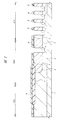
ここで、図3は次工程時における基板の要部平面図であり、図4および図5はそれぞれ図3中のA−A線およびB−B線に沿った断面図である。また、図4は、前工程の説明に用いた図2が示す断面と同じ断面を示している。なお、以降の工程を説明する各断面図において、Aの符号を付した図は図4と同じ断面を図示したものであり、Bの符号を付した図は図5と同じ断面を図示したものである。 Here, FIG. 3 is a plan view of the main part of the substrate in the next process, and FIGS. 4 and 5 are cross-sectional views taken along lines AA and BB in FIG. 3, respectively. FIG. 4 shows the same cross section as the cross section shown in FIG. 2 used for the description of the previous step. In each of the cross-sectional views for explaining the subsequent steps, the drawing with the symbol A shows the same cross section as FIG. 4, and the drawing with the reference B shows the same cross section as FIG. It is.
上記多結晶シリコン膜10を成膜した後、図3〜図5に示すように、フォトリソグラフィ技術によってパターニングされたフォトレジスト膜(図示は省略)によってゲート配線領域GLAを覆い、そのフォトレジスト膜をマスクとして多結晶シリコン膜10をエッチングする。それにより、活性セル領域ACAにおいては、多結晶シリコン膜10を溝部7内にのみ残し、溝部7内にてその多結晶シリコン膜10からゲート電極11を形成することができる。ゲート配線領域GLAにおいては、多結晶シリコン膜10は溝部8内を埋め込み、一部が溝部8内から連続して溝部8の外部に残るようにパターニングされ、ゲート電極11と電気的に接続するゲート引き出し電極12が形成される。また、溝部8外のゲート引き出し電極12には、ゲート引き出し電極12の端部から延在するスリット(第3溝部)14が形成される。このスリット14が延在する方向を溝部7、8が延在する方向(ゲート引き出し電極12が延在する方向)と交差する方向とすることにより、ゲート引き出し電極12がスリット14によって分断されてしまう不具合を防ぐことができる。ターミネーション領域TNAでは、多結晶シリコン膜10は除去される。
After the
ところで、d1は溝部8外における多結晶シリコン膜10(ゲート引き出し電極12)の膜厚であり、d2は溝部7内の多結晶シリコン膜10がオーバーエッチングされた量、すなわち溝部7の開口部から溝部7内の多結晶シリコン膜10(ゲート電極11)の表面までの深さである。本実施の形態1においては、スリット14の体積とゲート電極11より上の溝部7の体積とが同じとなるように、スリット14の幅および配置される間隔を設定する。
Incidentally, d1 is the film thickness of the polycrystalline silicon film 10 (gate lead electrode 12) outside the
次に、図6に示すように、基板に熱処理を施すことにより、膜厚20nm程度の酸化シリコン膜15を形成する。この時、溝部7付近を拡大した図7に示すように、溝部7の開口部からゲート電極11の表面までの側壁7Aにおいては、ゲート酸化膜9と酸化シリコン膜15とが二重に重なった状態で成膜される。
Next, as shown in FIG. 6, a
続いて、フォトリソグラフィ技術によってパターニングされたフォトレジスト膜(図示は省略)をマスクとしてn-型半導体領域5にp型の不純物(たとえばBF2(二フッ化ホウ素))を導入することにより、活性セル領域ACAのn-型半導体領域5にp+型半導体領域(第3半導体層)16を形成し、ターミネーション領域TNAにp+型ガードリング領域17を形成する。p+型半導体領域16は、本実施の形態1のトレンチゲート型パワーMISFETのソースとなる。p+型ガードリング領域17は、平面において活性セル領域ACAおよびゲート配線領域GLAを取り囲むように形成される。このp型の不純物を導入する工程時には、前述したように、溝部7の開口部からゲート電極11の表面までの側壁には、ゲート酸化膜9と酸化シリコン膜15との二重の酸化シリコン膜が成膜されている。それにより、p型の不純物が溝部7の側壁からn-型半導体領域5に導入されてしまうことを防ぎ、p+型半導体領域16の濃度プロファイルを最適化することが可能となる。すなわち、所望の形成範囲のp+型半導体領域16の下部に望ましくないp+型半導体領域16A(図7参照)が形成されてしまう不具合を未然に防ぐことが可能となる。また、p型の不純物が溝部7の側壁からゲート電極11に導入されてしまうことも防ぎ、ゲート耐圧を確保することができる。
Subsequently, by introducing a p-type impurity (for example, BF 2 (boron difluoride)) into the n − -
続いて、フォトリソグラフィ技術によってパターニングされたフォトレジスト膜(図示は省略)をマスクとしてn-型半導体領域5にn型の不純物(たとえばP(リン))を導入することにより、活性セル領域ACAのn-型半導体領域5にn+型半導体領域18を形成する。
Subsequently, an n-type impurity (for example, P (phosphorus)) is introduced into the n − -
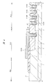
次に、図8および図9に示すように、CVD法で基板上に膜厚900Å〜1100Å程度の酸化シリコン膜19を堆積する。続いて、CVD法で酸化シリコン膜(第2絶縁膜)19上に膜厚4000Å〜5000Å程度のBPSG(Boro-Phospho Silicate Glass)膜(第2絶縁膜)20を堆積する。続いて、基板に900℃程度の熱処理を施すことにより、BPSG膜20を流動化させ、BPSG膜20の表面の段差を緩和する。
Next, as shown in FIGS. 8 and 9, a
ここで、BPSG膜20はゲート電極11上の溝部7内へ流れ込むため、溝部8外のゲート引き出し電極12にスリット14(図3および図5も参照)が形成されていない場合には、活性領セル域ACA(溝部7内を除く)における酸化シリコン膜15、酸化シリコン膜19およびBPSG膜20の総膜厚TC1は、その流れ込んだ分だけ他の領域、たとえばゲート配線領域GLAにおける酸化シリコン膜15、酸化シリコン膜19およびBPSG膜20の総膜厚TL1より薄くなる。一方、本実施の形態1では、スリット14が形成されていることから、BPSG膜20はこのスリット14に流れ込む。それにより、たとえばゲート配線領域GLAにおける酸化シリコン膜15、酸化シリコン膜19およびBPSG膜20の総膜厚TL1を活性セル領域ACA(溝部7内を除く)における酸化シリコン膜15、酸化シリコン膜19およびBPSG膜20の総膜厚TC1以下とすることが可能となる。これら各領域における酸化シリコン膜15、酸化シリコン膜19およびBPSG膜20の総膜厚と工程との関係については、次工程を説明する際にさらに詳しく説明する。
Here, since the
次に、図10〜図12に示すように、フォトリソグラフィ技術によってパターニングされたフォトレジスト膜(図示は省略)をマスクとしたエッチングにより、BPSG膜20、酸化シリコン膜19および酸化シリコン膜15をパターニングする。それにより、活性セル領域ACAにおいては、BPSG膜20、酸化シリコン膜19および酸化シリコン膜15がエッチバックされることになり、溝部7外のBPSG膜20、酸化シリコン膜19および酸化シリコン膜15は除去され、溝部7内にはそれらが所定量残される。ゲート配線領域GLAにおいては、溝部7外のBPSG膜20、酸化シリコン膜19および酸化シリコン膜15にゲート引き出し電極12に達する開口部(第1開口部)21が形成される。ターミネーション領域TNAにおいては、p+型ガードリング領域に達する開口部22が形成される。
Next, as shown in FIGS. 10 to 12, the
ところで、前述したようにスリット14が形成されていない場合には、活性セル領域ACA(溝部7内を除く)における酸化シリコン膜15、酸化シリコン膜19およびBPSG膜20の総膜厚TC1は、ゲート配線領域GLAにおける酸化シリコン膜15、酸化シリコン膜19およびBPSG膜20の総膜厚TL1より薄くなる。そのため、BPSG膜20、酸化シリコン膜19および酸化シリコン膜15をエッチングし、開口部21が完全にゲート引き出し電極12に達した時点において、ゲート電極11上のBPSG膜20、酸化シリコン膜19および酸化シリコン膜15の総膜厚が、所望のゲート耐圧を保つのに不十分となってしまう場合がある。一方、図8を用いて前述したように、本実施の形態1では、ゲート配線領域GLAにおける酸化シリコン膜15、酸化シリコン膜19およびBPSG膜20の総膜厚TL1を活性セル領域ACA(溝部7内を除く)における酸化シリコン膜15、酸化シリコン膜19およびBPSG膜20の総膜厚TC1以下とすることができる。そのような酸化シリコン膜15、酸化シリコン膜19およびBPSG膜20の総膜厚TC1、TL1とすることにより、BPSG膜20、酸化シリコン膜19および酸化シリコン膜15のパターニング時には、開口部21が完全にゲート引き出し電極12に達した時点でも、溝部7内の酸化シリコン膜15、酸化シリコン膜19およびBPSG膜20はエッチバックされることなく、溝部7内を完全に埋め込むように残すことができる。開口部21が完全にゲート引き出し電極12に達した後は、溝部7内の酸化シリコン膜15、酸化シリコン膜19およびBPSG膜20の総膜厚TG1が所望の膜厚となるまでエッチバックを進める。それにより、本実施の形態1のトレンチゲート型パワーMISFETにおいては、所望のゲート耐圧を確保することが可能となる。また、溝部7の開口部から溝部7内のゲート電極11の表面までの深さd2(図4参照)が、溝部8外におけるゲート引き出し電極12の膜厚d1(図4参照)と等しい場合には、スリット14の幅およびスリット14が配置される間隔を適当に設定し、たとえば溝部7とスリット14の幅とが同じ寸法となり、隣接する溝部7間の間隔と隣接するスリット14間の間隔とが同じ寸法となるようにすることにより、ゲート配線領域GLAにおける酸化シリコン膜15、酸化シリコン膜19およびBPSG膜20の総膜厚TL1を活性セル領域ACA(溝部7内を除く)における酸化シリコン膜15、酸化シリコン膜19およびBPSG膜20の総膜厚TC1と同等とすることができる。さらに、溝部8外におけるゲート引き出し電極12の膜厚d1(図4参照)が、溝部7の開口部から溝部7内のゲート電極11の表面までの深さd2(図4参照)より厚くなるように設定すれば、ゲート配線領域GLAにおける酸化シリコン膜15、酸化シリコン膜19およびBPSG膜20の総膜厚TL1を活性セル領域ACA(溝部7内を除く)における酸化シリコン膜15、酸化シリコン膜19およびBPSG膜20の総膜厚TC1以下とすることができる。
By the way, when the
また、本発明者らは、スリット14を形成しなくともゲート電極11の上面を溝部7の深さ方向に低くすることにより、開口部21が完全にゲート引き出し電極12に達した時点でも、溝部7内の酸化シリコン膜15、酸化シリコン膜19およびBPSG膜20の総膜厚TG1を所望のゲート耐圧を確保するのに十分な膜厚とすることができる技術について検討した。しかしながら、ゲート電極11の上面を溝部7の深さ方向に低くすると、ソースとなるp+型半導体領域16を深くする必要が生じる。ソースを深くするとパンチスルー耐圧が低下してしまうのでチャネルとなるn-型半導体領域5も深くする必要が生じる。チャネルとなるn-型半導体領域5を深くするとそれを貫く溝7も深くする必要がある。溝7が深くなることにより、ゲート・ソース間の寄生容量が増加してしまうためスイッチング損失が増加してしまうという不具合が生じる。また、溝7を深くすると浅いときに比べて深さばらつきが増えるため、溝部7のうち、トレンチゲート型パワーMISFETのチャネルとなるn-型半導体領域5を突き抜けてドレインとなるp-型単結晶シリコン層2に達する部分が増える。それにより、ゲート電極11とp-型単結晶シリコン層2との間に生じるゲート・ドレイン間の寄生容量が増加し、トレンチゲート型パワーMISFETのスイッチング損失が増加してしまう不具合が生じる。また、トレンチゲート型パワーMISFETのソースとなるp+型半導体領域16および前記n-型半導体領域5を深く形成するためにはp+型半導体領域16およびn-型半導体領域5を形成する不純物を拡散させるための熱処理に要する時間が増大し、半導体装置を製造するTAT(Turn Around Time)が増加してしまう不具合が生じる。また、溝部7を深く形成しなければいけないことから、溝部7の形状を制御することが困難になる上にエッチングに要する時間が増加し、半導体装置を製造するTAT(Turn Around Time)が増加してしまう不具合が生じる。一方、本実施の形態1によれば、溝部7を深く形成しなくとも、溝部7内の酸化シリコン膜15、酸化シリコン膜19およびBPSG膜20の総膜厚TG1を所望のゲート耐圧を確保するのに十分な膜厚とすることができるので、これらの不具合を解消することができる。また、本実施の形態1を適用しても、スリット14の形成は、多結晶シリコン10を成膜した後、フォトリソグラフィ技術によって、ゲート配線領域GLA及びゲート電極11以外の部分と同時に除去できるので、プロセス工程が増えることはない。
Further, the inventors reduce the upper surface of the
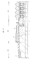
次に、図13および図14に示すように、基板上にバリア導体膜として、たとえばスパッタリング法で膜厚1000Å〜2200Å程度のTiW(チタンタングステン)膜23を堆積した後、基板に熱処理を施す。続いて、そのTiW膜23上に、たとえばスパッタリング法にて膜厚26000Å〜55000Å程度のAl(アルミニウム)膜24を堆積する。バリア導体膜は、Alと基板(Si)とが接触することにより不所望な反応層が形成されることを防止する役割を果たす。なお、本実施の形態1において、Al膜は、Alを主成分とする膜を意味し、他の金属等を含有していてもよい。続いて、フォトリソグラフィ技術によりパターニングされたフォトレジスト膜をマスクとしてそのTiW膜23およびAl膜24をエッチングすることにより、ゲート引き出し電極12と電気的に接続するゲート配線(第2配線)25、パワーMISFETのソース領域となるp+型半導体領域16と電気的に接続するソースパッド(ソース電極(第1配線))26、p+型ガードリング領域17と電気的に接続する配線27、およびゲート配線25と電気的に接続するゲートパッド(ゲート電極)を形成する。なお、そのゲートパッドは、図13および図14では図示されない領域に形成される。
Next, as shown in FIGS. 13 and 14, a TiW (titanium tungsten)
図示は省略するが、上記ゲート配線25、ソースパッド26、配線27およびゲートパッドを形成した後、基板の上部に、保護膜として、たとえばポリイミド樹脂膜を塗布し、露光、現像することによって、ゲートパッドおよびソースパッド26上のポリイミド樹脂膜を除去し、開口部を形成する。
Although illustration is omitted, after forming the
次いで、基板の表面をテープ等で保護した後、保護面を下側とし、p+型単結晶シリコン基板1の裏面を研削する。上記テープを剥がした後、p+型単結晶シリコン基板1の裏面上に、導電性膜として、たとえばTi(チタン)膜、Ni(ニッケル)膜およびAu(金)膜を順次スパッタリング法により堆積し、これらの積層膜を形成する。この積層膜は、ドレイン(p+型単結晶シリコン基板1およびp-型単結晶シリコン層2)の引出し電極(ドレイン電極)となる。
Next, after protecting the surface of the substrate with a tape or the like, the back surface of the p + type single
続いて、上記ポリイミド樹脂膜に形成した開口部上に、たとえばAu等よりなるバンプ電極を形成した後、ウエハ状態の基板を、たとえば分割領域(図示は省略)に沿ってダイシングし、個々のチップへと分割する。その後、個々のチップを、たとえば外部端子を有するリードフレーム(実装板)上に搭載し樹脂等で封止(実装)し、本実施の形態1の半導体装置を製造する。 Subsequently, a bump electrode made of, for example, Au or the like is formed on the opening formed in the polyimide resin film, and then the substrate in a wafer state is diced along, for example, divided regions (not shown) to obtain individual chips. Divide into Thereafter, the individual chips are mounted on, for example, a lead frame (mounting plate) having external terminals and sealed (mounted) with a resin or the like to manufacture the semiconductor device of the first embodiment.
(実施の形態2)
本実施の形態2の半導体装置は、前記実施の形態1の半導体装置と同様に、たとえばpチャネル型のパワーMISFETを有するものである。この本実施の形態2の半導体装置の製造方法について図15および図16を用いて説明する。
(Embodiment 2)
Similar to the semiconductor device of the first embodiment, the semiconductor device of the second embodiment has, for example, a p-channel type power MISFET. A method of manufacturing the semiconductor device according to the second embodiment will be described with reference to FIGS.
本実施の形態2の半導体装置の製造工程は、前記実施の形態1においてBPSG膜20を成膜した工程(図8および図9参照)までは同様であるが、ゲート引き出し電極12にスリット14(図3および図5参照)は形成しない。その後、図15に示すように、フォトリソグラフィ技術によってパターニングされたフォトレジスト膜R1によって基板上のゲート配線領域GLAおよびターミネーション領域TNAを覆い、活性セル領域ACAのBPSG膜20、酸化シリコン膜19および酸化シリコン膜15をエッチングする。それにより、活性セル領域ACAにおいては、溝部7外のBPSG膜20、酸化シリコン膜19および酸化シリコン膜15を除去し、溝部7内においては酸化シリコン膜15、酸化シリコン膜19およびBPSG膜20の総膜厚TG1を所望の膜厚とする。
The manufacturing process of the semiconductor device of the second embodiment is the same up to the process of forming the
次に、上記フォトレジスト膜R1を除去した後、図16に示すように、新たにフォトリソグラフィ技術によってパターニングされたフォトレジスト膜R2によって基板上の開口部21、22が形成される領域以外の領域を覆い、BPSG膜20、酸化シリコン膜19および酸化シリコン膜15をエッチングする。それにより、溝部7内のBPSG膜20および酸化シリコン膜19を目減りさせることなく開口部21、22を形成することができる。すなわち、本実施の形態2のトレンチゲート型パワーMISFETにおいても、所望のゲート耐圧を確保することが可能となる。
Next, after removing the photoresist film R1, as shown in FIG. 16, regions other than the regions where the
その後、前記実施の形態1にて図13および図14を用いて説明した工程と同様の工程を経ることにより、本実施の形態2の半導体装置を製造する。 Thereafter, the semiconductor device according to the second embodiment is manufactured through the same steps as those described with reference to FIGS. 13 and 14 in the first embodiment.
上記のような本実施の形態2によっても、前記実施の形態1と同様の効果を得ることができる。 According to the second embodiment as described above, the same effect as in the first embodiment can be obtained.
(実施の形態3)
本実施の形態3の半導体装置は、前記実施の形態1、2の半導体装置と同様に、たとえばpチャネル型のパワーMISFETを有するものである。この本実施の形態3の半導体装置の製造方法について図17および図18を用いて説明する。
(Embodiment 3)
The semiconductor device of the third embodiment has, for example, a p-channel type power MISFET, as in the semiconductor devices of the first and second embodiments. A method of manufacturing the semiconductor device according to the third embodiment will be described with reference to FIGS.
本実施の形態3の半導体装置の製造工程は、前記実施の形態1においてBPSG膜20を成膜した工程(図8および図9参照)までは同様であるが、ゲート引き出し電極12にスリット14(図3および図5参照)は形成しない。その後、図17に示すように、BPSG膜20および酸化シリコン膜19をエッチバックし、溝部7外のBPSG膜20および酸化シリコン膜19を除去する。ここで、溝部7内に残ったBPSG膜20、酸化シリコン膜19および酸化シリコン膜15の総膜厚を確認する。続いて、図18に示すように、基板上に酸化シリコン膜19と同様の酸化シリコン膜(第2絶縁膜、第3絶縁膜)19AおよびBPSG膜20と同様のBPSG膜(第2絶縁膜、第3絶縁膜)20Aを順次堆積し、基板に熱処理を施してBPSG膜20Aを流動化させる。
The manufacturing process of the semiconductor device of the third embodiment is the same up to the process of forming the
この時、BPSG膜20および酸化シリコン膜19をエッチバックした際に、溝部7内に残ったBPSG膜20、酸化シリコン膜19および酸化シリコン膜15の総膜厚が、所望のゲート耐圧を確保するのに十分であった場合には、BPSG膜20A、酸化シリコン膜19Aおよび酸化シリコン膜15をエッチングして開口部21、22を形成し、その後、前記実施の形態1にて図13および図14を用いて説明した工程と同様の工程を経ることにより、本実施の形態3の半導体装置を製造する。一方、BPSG膜20および酸化シリコン膜19をエッチバックした際に、溝部7内に残ったBPSG膜20、酸化シリコン膜19および酸化シリコン膜15の総膜厚が、所望のゲート耐圧を確保するのに十分でない場合には、BPSG膜20Aおよび酸化シリコン膜19Aをエッチバックし、溝部7外のBPSG膜20Aおよび酸化シリコン膜19Aを除去する。ここで、溝部7内に残ったBPSG膜20、20A、酸化シリコン膜19、19Aおよび酸化シリコン膜15の総膜厚を確認し、所望のゲート耐圧を確保するのに十分でない場合には、十分な総膜厚となるまで、酸化シリコン膜19AおよびBPSG膜20Aを堆積する工程と、この積層膜をエッチバックする工程とを繰り返した後に開口部21、22を形成する。このような本実施の形態3のトレンチゲート型パワーMISFETにおいても、所望のゲート耐圧を確保することが可能となる。
At this time, when the
(実施の形態4)
本実施の形態4の半導体装置は、前記実施の形態1〜3の半導体装置と同様に、たとえばpチャネル型のパワーMISFETを有するものである。この本実施の形態4の半導体装置の製造方法について図19および図20を用いて説明する。
(Embodiment 4)
The semiconductor device of the fourth embodiment has, for example, a p-channel type power MISFET, like the semiconductor devices of the first to third embodiments. A method of manufacturing the semiconductor device according to the fourth embodiment will be described with reference to FIGS.
本実施の形態4の半導体装置の製造工程は、前記実施の形態1の半導体装置の製造工程とほぼ同様であるが、図19に示すように、ゲート引き出し電極12に前記実施の形態1で形成したスリット14(図3および図5参照)の代わりに複数の平面円形の開口部(第3溝部)14Aを形成する。この開口部14Aの開口径は、スリット14の幅と同程度とすることを例示できる。スリット14の代わりに平面円形の開口部14Aを形成することにより、後の工程で形成されるゲート配線25(図13および図14参照)とゲート引き出し電極12とが接触する面積を増加することができる。それにより、ゲート抵抗を低減することができる。
The manufacturing process of the semiconductor device according to the fourth embodiment is almost the same as the manufacturing process of the semiconductor device according to the first embodiment. However, as shown in FIG. Instead of the slits 14 (see FIGS. 3 and 5), a plurality of planar circular openings (third groove portions) 14A are formed. It can be exemplified that the opening diameter of the
また、図20に示すように、スリット14の代わりに、ゲート引き出し電極12の端部まで達していないスリット(第3溝部)14Bを形成してもよい。このように、平面で周囲をゲート引き出し電極12に囲まれたスリット14Bとすることにより、ゲート引き出し電極12は、電流経路と直行する方向での断面積を増加できるので、ゲート抵抗を低減することができる。また、この電流経路と直行する方向での断面積を増加できるという観点では、上記の平面円形の開口部14Aを形成した場合でも同様の効果を得ることをできる。
Further, as shown in FIG. 20, a slit (third groove portion) 14 </ b> B that does not reach the end of the
以上、本発明者によってなされた発明を実施の形態に基づき具体的に説明したが、本発明は前記実施の形態に限定されるものではなく、その要旨を逸脱しない範囲で種々変更可能であることはいうまでもない。 As mentioned above, the invention made by the present inventor has been specifically described based on the embodiment. However, the present invention is not limited to the embodiment, and various modifications can be made without departing from the scope of the invention. Needless to say.
たとえば、前記実施の形態では、トレンチゲート型パワーMISFETを含む半導体装置の製造工程について説明したが、同様に基板に形成された溝部内にゲート電極を有するIGBT(Insulated Gate Bipolar Transistor)を含む半導体装置の製造工程に対しても同様の製造工程を適用することができる。 For example, in the above embodiment, the manufacturing process of a semiconductor device including a trench gate type power MISFET has been described. Similarly, a semiconductor device including an IGBT (Insulated Gate Bipolar Transistor) having a gate electrode in a groove formed in a substrate. The same manufacturing process can be applied to this manufacturing process.
本発明の半導体装置の製造方法は、たとえばトレンチゲート型のパワーMISFETを有する半導体装置の製造工程に適用することができる。 The semiconductor device manufacturing method of the present invention can be applied to a manufacturing process of a semiconductor device having, for example, a trench gate type power MISFET.
1 p+型単結晶シリコン基板
2 p-型単結晶シリコン層(第1半導体層)
3 酸化シリコン膜
4 フィールド絶縁膜
5 n-型半導体領域(第2半導体層)
6 酸化シリコン膜
7 溝部(第1溝部)
7A 側壁
8 溝部(第2溝部)
9 ゲート酸化膜(第1絶縁膜)
10 多結晶シリコン膜(第1導電性膜)
11 ゲート電極
12 ゲート引き出し電極
14 スリット(第3溝部)
14A 開口部(第3溝部)
14B スリット(第3溝部)
15 酸化シリコン膜
16 p+型半導体領域(第3半導体層)
17 p+型ガードリング領域
18 n+型半導体領域
19 酸化シリコン膜(第2絶縁膜)
19A 酸化シリコン膜(第2絶縁膜、第3絶縁膜)
20 BPSG膜(第2絶縁膜)
20A BPSG膜(第2絶縁膜、第3絶縁膜)
21 開口部(第1開口部)
22 開口部
23 TiW膜
24 Al膜
25 ゲート配線(第2配線)
26 ソースパッド(ソース電極(第1配線))
27 配線
101 基板
102、103 溝
104 ゲート電極
105 ゲート配線
106 層間絶縁膜
107 開口部
108、109、110 半導体層
ACA 活性セル領域(第1領域)
GLA ゲート配線領域(第2領域)
R1、R2 フォトレジスト膜
TC、TL、TG 膜厚
TC1、TL1、TG1 膜厚
TNA ターミネーション領域
1 p + type single crystal silicon substrate 2 p − type single crystal silicon layer (first semiconductor layer)
3
6 Silicon oxide film 7 Groove (first groove)
9 Gate oxide film (first insulating film)
10 Polycrystalline silicon film (first conductive film)
11
14A opening (third groove)
14B Slit (third groove)
15 Silicon oxide film 16 p + type semiconductor region (third semiconductor layer)
17 p + type guard ring region 18 n +
19A Silicon oxide film (second insulating film, third insulating film)
20 BPSG film (second insulating film)
20A BPSG film (second insulating film, third insulating film)
21 opening (first opening)
22
26 Source pad (source electrode (first wiring))
27
GLA gate wiring area (second area)
R1, R2 Photoresist film TC, TL, TG film thickness TC1, TL1, TG1 film thickness TNA termination region
Claims (12)
(a)第1導電型の半導体基板の主面に第1導電型の第1半導体層を形成する工程、
(b)前記半導体基板に前記第1導電型とは逆の極性の第2導電型の不純物を導入して第2導電型の第2半導体層を形成する工程、
(c)前記半導体基板の主面において、第1領域に前記第2半導体層を貫通する第1溝部を形成し、第2領域に前記第2半導体層を貫通する第2溝部を形成する工程、
(d)前記第1溝部内および前記第2溝部内に第1絶縁膜を形成する工程、
(e)前記第1絶縁膜の存在下で、前記第1溝部外および前記第2溝部外を含む前記半導体基板上に第1導電性膜を形成すると共に、前記第1溝部内および前記第2溝部内を前記第1導電性膜で埋め込む工程、
(f)前記第1導電性膜をパターニングし、前記第1領域においては前記第1溝部外の前記第1導電性膜と前記第1溝部の開口部から第1の深さ分だけの前記第1導電性膜とを除去し、前記第2領域においては前記第2溝部を埋め込み前記第2溝部外へ所定量延在する前記第1導電性膜を残すと共に、前記第2溝部外へ延在する前記第1導電性膜に第3溝部を形成する工程、
(g)前記第1領域の前記第2半導体層に第1導電型の不純物を導入し、前記第1溝部と隣接する前記第2半導体層に第1導電型の第3半導体層を形成する工程、
(h)前記(f)工程後、前記第2領域における前記第1導電性膜上での膜厚が前記第1領域での膜厚以下となるように、前記第1溝部外を含む前記半導体基板上に第2絶縁膜をCVD法によって形成すると共に、前記第1溝部内および前記第3溝部内を前記第2絶縁膜で埋め込む工程、
(i)前記第2絶縁膜をパターニングし、前記第1領域においては前記第1溝部外の前記第2絶縁膜を除去しつつ前記第1溝部内に前記第2絶縁膜を残し、前記第2領域においては前記第3溝部内に前記第2絶縁膜を残しつつ、前記第2絶縁膜に前記第2溝部外へ延在する前記第1導電性膜に達する第1開口部を形成する工程、
(j)前記(i)工程後、前記第1領域の前記半導体基板上に前記第3半導体層と電気的に接続する第1配線を形成し、前記第2領域の前記半導体基板上に前記第1開口部下で前記第1導電性膜と電気的に接続する第2配線を形成する工程、
を含み、
前記第1領域にて、前記第1半導体層をドレインとし、前記第2半導体層をチャネルとし、前記第3半導体層をソースとすることを特徴とする半導体装置の製造方法。 A method for manufacturing a semiconductor device, comprising:
(A) forming a first conductivity type first semiconductor layer on a main surface of a first conductivity type semiconductor substrate;
(B) introducing a second conductivity type impurity having a polarity opposite to the first conductivity type into the semiconductor substrate to form a second conductivity type second semiconductor layer;
(C) forming a first groove portion penetrating the second semiconductor layer in a first region and forming a second groove portion penetrating the second semiconductor layer in a second region on the main surface of the semiconductor substrate;
(D) forming a first insulating film in the first groove and in the second groove;
(E) In the presence of the first insulating film, a first conductive film is formed on the semiconductor substrate including the outside of the first groove and the outside of the second groove, and the inside of the first groove and the second Filling the groove with the first conductive film;
(F) patterning the first conductive film, and in the first region, the first conductive film outside the first groove and the first depth from the opening of the first groove by a first depth; 1 conductive film is removed, and in the second region, the second groove portion is embedded, leaving the first conductive film extending a predetermined amount outside the second groove portion, and extending outside the second groove portion. Forming a third groove in the first conductive film;
(G) introducing a first conductivity type impurity into the second semiconductor layer in the first region, and forming a first conductivity type third semiconductor layer in the second semiconductor layer adjacent to the first groove portion; ,
(H) wherein (f) after the step, as the film thickness on the first conductive film before the SL second region becomes equal to or less than the thickness at the first area, wherein including said first groove outer Forming a second insulating film on the semiconductor substrate by a CVD method and embedding the first groove and the third groove with the second insulating film;
(I) patterning the second insulating film, removing the second insulating film outside the first groove part in the first region, leaving the second insulating film in the first groove part, Forming a first opening reaching the first conductive film extending out of the second groove in the second insulating film while leaving the second insulating film in the third groove in the region;
(J) After the step (i), a first wiring electrically connected to the third semiconductor layer is formed on the semiconductor substrate in the first region, and the first wiring is formed on the semiconductor substrate in the second region. Forming a second wiring electrically connected to the first conductive film under one opening;
Including
A method of manufacturing a semiconductor device, wherein, in the first region, the first semiconductor layer is a drain, the second semiconductor layer is a channel, and the third semiconductor layer is a source.
前記第3溝部は、前記第1導電性膜上の前記第1溝部の体積と同じ体積となるように形成することを特徴とする半導体装置の製造方法。 In the manufacturing method of the semiconductor device according to claim 1,
The method of manufacturing a semiconductor device, wherein the third groove portion is formed to have the same volume as the volume of the first groove portion on the first conductive film.
前記第3溝部の深さは、前記第1の深さ以上であることを特徴とする半導体装置の製造方法。 In the manufacturing method of the semiconductor device according to claim 1 or 2,
The method of manufacturing a semiconductor device, wherein a depth of the third groove portion is equal to or greater than the first depth.
前記第1溝部は、前記第1溝部が延在する方向と交差する第1方向での前記半導体基板の第1断面において複数配置されるように形成し、
前記第3溝部は、複数配置されるように形成し、
前記第1溝部の幅と前記第3溝部の幅とが同じとなるように形成し、
前記第1断面で隣接する前記第1溝部の間隔と隣接する前記第3溝部の間隔とが同じとなるように形成することを特徴とする半導体装置の製造方法。 In the manufacturing method of the semiconductor device of any one of Claims 1-3,
A plurality of the first groove portions are formed in a first cross section of the semiconductor substrate in a first direction intersecting a direction in which the first groove portions extend;
The third groove is formed so as to be arranged in a plurality,
Forming the first groove and the third groove to have the same width;
A method of manufacturing a semiconductor device, characterized in that the interval between the first groove portions adjacent in the first cross section is the same as the interval between the adjacent third groove portions.
平面形状にて、前記第3溝部は、前記第1開口部が延在する方向と交差するように形成することを特徴とする半導体装置の製造方法。 In the manufacturing method of the semiconductor device given in any 1 paragraph of Claims 1-4,
The method of manufacturing a semiconductor device, wherein the third groove is formed in a planar shape so as to intersect a direction in which the first opening extends.
前記第3溝部は、平面形状が前記第1導電性膜に囲まれるように形成することを特徴とする半導体装置の製造方法。 In the manufacturing method of the semiconductor device according to any one of claims 1 to 5,
The method of manufacturing a semiconductor device, wherein the third groove portion is formed so that a planar shape is surrounded by the first conductive film.
前記第3溝部は、平面形状が円形となるように形成することを特徴とする半導体装置の製造方法。 The method of manufacturing a semiconductor device according to claim 6.
The method of manufacturing a semiconductor device, wherein the third groove portion is formed so as to have a circular planar shape.
前記第1導電性膜は、ゲートとすることを特徴とする半導体装置の製造方法。 In the manufacturing method of the semiconductor device of any one of Claims 1-7,
The method of manufacturing a semiconductor device, wherein the first conductive film is a gate.
(a)第1導電型の半導体基板の主面に第1導電型の第1半導体層を形成する工程、
(b)前記半導体基板に前記第1導電型とは逆の極性の第2導電型の不純物を導入して第2導電型の第2半導体層を形成する工程、
(c)前記半導体基板の主面において、第1領域に前記第2半導体層を貫通する第1溝部を形成し、第2領域に前記第2半導体層を貫通する第2溝部を形成する工程、
(d)前記第1溝部内および前記第2溝部内に第1絶縁膜を形成する工程、
(e)前記第1絶縁膜の存在下で、前記第1溝部外および前記第2溝部外を含む前記半導体基板上に第1導電性膜を形成すると共に、前記第1溝部内および前記第2溝部内を前記第1導電性膜で埋め込む工程、
(f)前記第1導電性膜をパターニングし、前記第1領域においては前記第1溝部外の前記第1導電性膜と前記第1溝部の開口部から第1の深さ分だけの前記第1導電性膜とを除去し、前記第2領域においては前記第2溝部を埋め込み前記第2溝部外へ所定量延在する前記第1導電性膜を残す工程、
(g)前記第1領域の前記第2半導体層に第1導電型の不純物を導入し、前記第1溝部と隣接する前記第2半導体層に第1導電型の第3半導体層を形成する工程、
(h)前記(f)工程後、前記第2領域における前記第1導電性膜上での膜厚が前記第1領域での膜厚以下となるように、前記第1溝部外を含む前記半導体基板上に第2絶縁膜を形成すると共に、前記第1溝部内を前記第2絶縁膜で埋め込む工程、
(i)前記第1領域の前記第2絶縁膜をパターニングし、前記第1溝部外の前記第2絶縁膜を除去しつつ、前記第1溝部内に前記第2絶縁膜を残す工程、
(j)前記(i)工程の前または後に、前記第2領域の前記第2絶縁膜をパターニングし、前記第2絶縁膜に前記第2溝部外へ延在する前記第1導電性膜に達する第1開口部を形成する工程、
(k)前記(i)工程および前記(j)工程後、前記第1領域の前記半導体基板上に前記第3半導体層と電気的に接続する第1配線を形成し、前記第2領域の前記半導体基板上に前記第1開口部下で前記第1導電性膜と電気的に接続する第2配線を形成する工程、
を含み、
前記第1領域にて、前記第1半導体層をドレインとし、前記第2半導体層をチャネルとし、前記第3半導体層をソースとすることを特徴とする半導体装置の製造方法。 A method for manufacturing a semiconductor device, comprising:
(A) forming a first conductivity type first semiconductor layer on a main surface of a first conductivity type semiconductor substrate;
(B) introducing a second conductivity type impurity having a polarity opposite to the first conductivity type into the semiconductor substrate to form a second conductivity type second semiconductor layer;
(C) forming a first groove portion penetrating the second semiconductor layer in a first region and forming a second groove portion penetrating the second semiconductor layer in a second region on the main surface of the semiconductor substrate;
(D) forming a first insulating film in the first groove and in the second groove;
(E) In the presence of the first insulating film, a first conductive film is formed on the semiconductor substrate including the outside of the first groove and the outside of the second groove, and the inside of the first groove and the second Filling the groove with the first conductive film;
(F) patterning the first conductive film, and in the first region, the first conductive film outside the first groove and the first depth from the opening of the first groove by a first depth; 1 and a conductive film is removed, as the second residue to Engineering said first conductive film by a predetermined amount extending into the second groove outer embedding the second groove in the region,
(G) introducing a first conductivity type impurity into the second semiconductor layer in the first region, and forming a first conductivity type third semiconductor layer in the second semiconductor layer adjacent to the first groove portion; ,
(H) After the step (f), the semiconductor including the outside of the first groove so that a film thickness on the first conductive film in the second region is equal to or less than a film thickness in the first region. Forming a second insulating film on the substrate and filling the first groove with the second insulating film;
(I) patterning the second insulating film in the first region, removing the second insulating film outside the first groove, and leaving the second insulating film in the first groove ;
(J) Before or after the step (i), the second insulating film in the second region is patterned to reach the first conductive film extending outside the second groove in the second insulating film. Forming a first opening;
(K) After the step (i) and the step (j), a first wiring electrically connected to the third semiconductor layer is formed on the semiconductor substrate in the first region, and the second region Forming a second wiring electrically connected to the first conductive film under the first opening on the semiconductor substrate;
Including
A method of manufacturing a semiconductor device, wherein, in the first region, the first semiconductor layer is a drain, the second semiconductor layer is a channel, and the third semiconductor layer is a source.
前記第1導電性膜は、ゲートとすることを特徴とする半導体装置の製造方法。 In the manufacturing method of the semiconductor device according to claim 9,
The method of manufacturing a semiconductor device, wherein the first conductive film is a gate.
(a)第1導電型の半導体基板の主面に第1導電型の第1半導体層を形成する工程、
(b)前記半導体基板に前記第1導電型とは逆の極性の第2導電型の不純物を導入して第2導電型の第2半導体層を形成する工程、
(c)前記半導体基板の主面において、第1領域に前記第2半導体層を貫通する第1溝部を形成し、第2領域に前記第2半導体層を貫通する第2溝部を形成する工程、
(d)前記第1溝部内および前記第2溝部内に第1絶縁膜を形成する工程、
(e)前記第1絶縁膜の存在下で、前記第1溝部外および前記第2溝部外を含む前記半導体基板上に第1導電性膜を形成すると共に、前記第1溝部内および前記第2溝部内を前記第1導電性膜で埋め込む工程、
(f)前記第1導電性膜をパターニングし、前記第1領域においては前記第1溝部外の前記第1導電性膜と前記第1溝部の開口部から第1の深さ分だけの前記第1導電性膜とを除去し、前記第2領域においては前記第2溝部を埋め込み前記第2溝部外へ所定量延在する前記第1導電性膜を残す工程、
(g)前記第1領域の前記第2半導体層に第1導電型の不純物を導入し、前記第1溝部と隣接する前記第2半導体層に第1導電型の第3半導体層を形成する工程、
(h)前記(f)工程後、前記第2領域における前記第1導電性膜上での膜厚が前記第1領域での膜厚以下となるように、前記第1溝部外を含む前記半導体基板上に第2絶縁膜を形成すると共に、前記第1溝部内を前記第2絶縁膜で埋め込む工程、
(i)前記半導体基板の全面において、前記第1溝部外の前記第2絶縁膜が除去されるまで前記第2絶縁膜をエッチングする工程、
(j)前記(i)工程後において前記第1溝部が前記第2絶縁膜で埋め込まれるまで前記(h)工程および前記(i)工程を繰り返す工程、
(k)前記(h)工程後、前記半導体基板上に第3絶縁膜を形成する工程、
(l)前記第3絶縁膜をパターニングし、前記第1領域においては前記第3絶縁膜を除去し、前記第2領域においては前記第3絶縁膜に前記第2溝部外へ延在する前記第1導電性膜に達する第1開口部を形成する工程、
(m)前記(l)工程後、前記第1領域の前記半導体基板上に前記第3半導体層と電気的に接続する第1配線を形成し、前記第2領域の前記半導体基板上に前記第1開口部下で前記第1導電性膜と電気的に接続する第2配線を形成する工程、
を含み、
前記第1領域にて、前記第1半導体層をドレインとし、前記第2半導体層をチャネルとし、前記第3半導体層をソースとすることを特徴とする半導体装置の製造方法。 A method for manufacturing a semiconductor device, comprising:
(A) forming a first conductivity type first semiconductor layer on a main surface of a first conductivity type semiconductor substrate;
(B) introducing a second conductivity type impurity having a polarity opposite to the first conductivity type into the semiconductor substrate to form a second conductivity type second semiconductor layer;
(C) forming a first groove portion penetrating the second semiconductor layer in a first region and forming a second groove portion penetrating the second semiconductor layer in a second region on the main surface of the semiconductor substrate;
(D) forming a first insulating film in the first groove and in the second groove;
(E) In the presence of the first insulating film, a first conductive film is formed on the semiconductor substrate including the outside of the first groove and the outside of the second groove, and the inside of the first groove and the second Filling the groove with the first conductive film;
(F) patterning the first conductive film, and in the first region, the first conductive film outside the first groove and the first depth from the opening of the first groove by a first depth; 1 and a conductive film is removed, as the second residue to Engineering said first conductive film by a predetermined amount extending into the second groove outer embedding the second groove in the region,
(G) introducing a first conductivity type impurity into the second semiconductor layer in the first region, and forming a first conductivity type third semiconductor layer in the second semiconductor layer adjacent to the first groove portion; ,
(H) After the step (f), the semiconductor including the outside of the first groove so that a film thickness on the first conductive film in the second region is equal to or less than a film thickness in the first region. Forming a second insulating film on the substrate and filling the first groove with the second insulating film;
(I) etching the second insulating film on the entire surface of the semiconductor substrate until the second insulating film outside the first groove is removed;
(J) repeating the step (h) and the step (i) until the first groove is filled with the second insulating film after the step (i),
(K) after the step (h), forming a third insulating film on the semiconductor substrate;
(L) The third insulating film is patterned, the third insulating film is removed in the first region, and the third insulating film extends outside the second groove in the second region. Forming a first opening reaching one conductive film;
(M) After the step (l), a first wiring electrically connected to the third semiconductor layer is formed on the semiconductor substrate in the first region, and the first wiring is formed on the semiconductor substrate in the second region. Forming a second wiring electrically connected to the first conductive film under one opening;
Including
A method of manufacturing a semiconductor device, wherein, in the first region, the first semiconductor layer is a drain, the second semiconductor layer is a channel, and the third semiconductor layer is a source.
前記第1導電性膜は、ゲートとすることを特徴とする半導体装置の製造方法。 The method of manufacturing a semiconductor device according to claim 11.
The method of manufacturing a semiconductor device, wherein the first conductive film is a gate.
Priority Applications (3)
| Application Number | Priority Date | Filing Date | Title |
|---|---|---|---|
| JP2004188290A JP4860122B2 (en) | 2004-06-25 | 2004-06-25 | Manufacturing method of semiconductor device |
| US11/144,623 US7271068B2 (en) | 2004-06-25 | 2005-06-06 | Method of manufacture of semiconductor device |
| US11/849,015 US7659574B2 (en) | 2004-06-25 | 2007-08-31 | Manufacturing method of semiconductor device |
Applications Claiming Priority (1)
| Application Number | Priority Date | Filing Date | Title |
|---|---|---|---|
| JP2004188290A JP4860122B2 (en) | 2004-06-25 | 2004-06-25 | Manufacturing method of semiconductor device |
Related Child Applications (1)
| Application Number | Title | Priority Date | Filing Date |
|---|---|---|---|
| JP2011145659A Division JP2011216901A (en) | 2011-06-30 | 2011-06-30 | Semiconductor device |
Publications (3)
| Publication Number | Publication Date |
|---|---|
| JP2006013136A JP2006013136A (en) | 2006-01-12 |
| JP2006013136A5 JP2006013136A5 (en) | 2007-08-09 |
| JP4860122B2 true JP4860122B2 (en) | 2012-01-25 |
Family
ID=35506403
Family Applications (1)
| Application Number | Title | Priority Date | Filing Date |
|---|---|---|---|
| JP2004188290A Active JP4860122B2 (en) | 2004-06-25 | 2004-06-25 | Manufacturing method of semiconductor device |
Country Status (2)
| Country | Link |
|---|---|
| US (2) | US7271068B2 (en) |
| JP (1) | JP4860122B2 (en) |
Families Citing this family (15)
| Publication number | Priority date | Publication date | Assignee | Title |
|---|---|---|---|---|
| KR100536042B1 (en) * | 2004-06-11 | 2005-12-12 | 삼성전자주식회사 | Method for forming recess gate electrode in semiconductor process |
| JP2006196545A (en) * | 2005-01-11 | 2006-07-27 | Toshiba Corp | Method of manufacturing semiconductor device |
| JP4955222B2 (en) | 2005-05-20 | 2012-06-20 | ルネサスエレクトロニクス株式会社 | Manufacturing method of semiconductor device |
| JP5198752B2 (en) * | 2006-09-28 | 2013-05-15 | ルネサスエレクトロニクス株式会社 | Manufacturing method of semiconductor device |
| JP5198760B2 (en) * | 2006-12-08 | 2013-05-15 | ルネサスエレクトロニクス株式会社 | Semiconductor device and manufacturing method thereof |
| JP5210564B2 (en) * | 2007-07-27 | 2013-06-12 | ルネサスエレクトロニクス株式会社 | Semiconductor device |
| JP2009199999A (en) * | 2008-02-25 | 2009-09-03 | Canon Inc | Image display apparatus |
| JP5423018B2 (en) * | 2009-02-02 | 2014-02-19 | 三菱電機株式会社 | Semiconductor device |
| JP5370480B2 (en) * | 2009-04-30 | 2013-12-18 | 三菱電機株式会社 | Semiconductor device and manufacturing method thereof |
| US20110084332A1 (en) * | 2009-10-08 | 2011-04-14 | Vishay General Semiconductor, Llc. | Trench termination structure |
| US9653597B2 (en) | 2010-05-20 | 2017-05-16 | Infineon Technologies Americas Corp. | Method for fabricating a shallow and narrow trench FET and related structures |
| US20140264588A1 (en) * | 2013-03-14 | 2014-09-18 | Taiwan Semiconductor Manufacturing Co. Ltd. | Metal Oxide Semiconductor Field-Effect Transistor (MOSFET) with Step Oxide |
| KR102030437B1 (en) | 2013-07-05 | 2019-10-10 | 삼성전자주식회사 | Semiconductor device |
| DE102013217709A1 (en) | 2013-09-05 | 2015-03-05 | Carl Zeiss Microscopy Gmbh | Lighting device and digital profile projector |
| CN112992682A (en) * | 2019-12-13 | 2021-06-18 | 华润微电子(重庆)有限公司 | Groove type field effect transistor structure and preparation method thereof |
Family Cites Families (17)
| Publication number | Priority date | Publication date | Assignee | Title |
|---|---|---|---|---|
| JP2586705B2 (en) * | 1990-08-13 | 1997-03-05 | 日本電気株式会社 | Semiconductor device and manufacturing method thereof |
| US5282018A (en) * | 1991-01-09 | 1994-01-25 | Kabushiki Kaisha Toshiba | Power semiconductor device having gate structure in trench |
| JPH07335871A (en) * | 1994-06-15 | 1995-12-22 | Hitachi Ltd | Insulated gate semiconductor device and its manufacturing method |
| US5597765A (en) * | 1995-01-10 | 1997-01-28 | Siliconix Incorporated | Method for making termination structure for power MOSFET |
| JPH09162188A (en) * | 1995-12-13 | 1997-06-20 | Sony Corp | Semiconductor device and fabrication thereof |
| JPH09326434A (en) * | 1996-06-04 | 1997-12-16 | Sony Corp | Semiconductor device and manufacture thereof |
| JP3395603B2 (en) * | 1997-09-26 | 2003-04-14 | 株式会社豊田中央研究所 | Semiconductor device including lateral MOS element |
| US6031265A (en) * | 1997-10-16 | 2000-02-29 | Magepower Semiconductor Corp. | Enhancing DMOS device ruggedness by reducing transistor parasitic resistance and by inducing breakdown near gate runners and termination area |
| JP3413569B2 (en) * | 1998-09-16 | 2003-06-03 | 株式会社日立製作所 | Insulated gate semiconductor device and method of manufacturing the same |
| JP2001267538A (en) * | 2000-03-15 | 2001-09-28 | Nec Corp | Manufacturing method of semiconductor device |
| US6465325B2 (en) * | 2001-02-27 | 2002-10-15 | Fairchild Semiconductor Corporation | Process for depositing and planarizing BPSG for dense trench MOSFET application |
| JP4608133B2 (en) | 2001-06-08 | 2011-01-05 | ルネサスエレクトロニクス株式会社 | Semiconductor device provided with vertical MOSFET and manufacturing method thereof |
| JP4854868B2 (en) * | 2001-06-14 | 2012-01-18 | ローム株式会社 | Semiconductor device |
| US7045859B2 (en) * | 2001-09-05 | 2006-05-16 | International Rectifier Corporation | Trench fet with self aligned source and contact |
| JP4740523B2 (en) * | 2003-01-27 | 2011-08-03 | ルネサスエレクトロニクス株式会社 | Insulated gate semiconductor device |
| JP4860102B2 (en) * | 2003-06-26 | 2012-01-25 | ルネサスエレクトロニクス株式会社 | Semiconductor device |
| JP4945055B2 (en) * | 2003-08-04 | 2012-06-06 | ルネサスエレクトロニクス株式会社 | Semiconductor device and manufacturing method thereof |
-
2004
- 2004-06-25 JP JP2004188290A patent/JP4860122B2/en active Active
-
2005
- 2005-06-06 US US11/144,623 patent/US7271068B2/en active Active
-
2007
- 2007-08-31 US US11/849,015 patent/US7659574B2/en active Active
Also Published As
| Publication number | Publication date |
|---|---|
| US20080173938A1 (en) | 2008-07-24 |
| JP2006013136A (en) | 2006-01-12 |
| US20050287732A1 (en) | 2005-12-29 |
| US7271068B2 (en) | 2007-09-18 |
| US7659574B2 (en) | 2010-02-09 |
Similar Documents
| Publication | Publication Date | Title |
|---|---|---|
| US7659574B2 (en) | Manufacturing method of semiconductor device | |
| JP4860102B2 (en) | Semiconductor device | |
| JP4892172B2 (en) | Semiconductor device and manufacturing method thereof | |
| US9793342B2 (en) | Insulated gate type semiconductor device and method for fabricating the same | |
| WO2016080269A1 (en) | Semiconductor device and method for producing semiconductor device | |
| US7494876B1 (en) | Trench-gated MIS device having thick polysilicon insulation layer at trench bottom and method of fabricating the same | |
| JP6324838B2 (en) | Semiconductor device and manufacturing method thereof | |
| US7508030B2 (en) | Semiconductor device with vertical MOSFET and method of manufacturing the same | |
| JP5420225B2 (en) | Semiconductor device and manufacturing method thereof | |
| JP2005079462A (en) | Semiconductor device and method for manufacturing the same | |
| JP5096675B2 (en) | Semiconductor device manufacturing method and semiconductor device | |
| JP2007053226A (en) | Semiconductor device and its manufacturing method | |
| JP2011029675A (en) | Semiconductor device | |
| JP2011216901A (en) | Semiconductor device | |
| JP2007036299A (en) | Semiconductor device and method for fabricating the same | |
| JP2006156571A (en) | Manufacturing method of semiconductor device |
Legal Events
| Date | Code | Title | Description |
|---|---|---|---|
| A521 | Written amendment |
Free format text: JAPANESE INTERMEDIATE CODE: A523 Effective date: 20070622 |
|
| A621 | Written request for application examination |
Free format text: JAPANESE INTERMEDIATE CODE: A621 Effective date: 20070622 |
|
| A711 | Notification of change in applicant |
Free format text: JAPANESE INTERMEDIATE CODE: A712 Effective date: 20100528 |
|
| A977 | Report on retrieval |
Free format text: JAPANESE INTERMEDIATE CODE: A971007 Effective date: 20110425 |
|
| A131 | Notification of reasons for refusal |
Free format text: JAPANESE INTERMEDIATE CODE: A131 Effective date: 20110510 |
|
| A521 | Written amendment |
Free format text: JAPANESE INTERMEDIATE CODE: A523 Effective date: 20110630 |
|
| A131 | Notification of reasons for refusal |
Free format text: JAPANESE INTERMEDIATE CODE: A131 Effective date: 20110719 |
|
| A521 | Written amendment |
Free format text: JAPANESE INTERMEDIATE CODE: A523 Effective date: 20110906 |
|
| TRDD | Decision of grant or rejection written | ||
| A01 | Written decision to grant a patent or to grant a registration (utility model) |
Free format text: JAPANESE INTERMEDIATE CODE: A01 Effective date: 20111011 |
|
| A01 | Written decision to grant a patent or to grant a registration (utility model) |
Free format text: JAPANESE INTERMEDIATE CODE: A01 |
|
| A61 | First payment of annual fees (during grant procedure) |
Free format text: JAPANESE INTERMEDIATE CODE: A61 Effective date: 20111102 |
|
| R150 | Certificate of patent or registration of utility model |
Ref document number: 4860122 Country of ref document: JP Free format text: JAPANESE INTERMEDIATE CODE: R150 Free format text: JAPANESE INTERMEDIATE CODE: R150 |
|
| FPAY | Renewal fee payment (event date is renewal date of database) |
Free format text: PAYMENT UNTIL: 20141111 Year of fee payment: 3 |
|
| S531 | Written request for registration of change of domicile |
Free format text: JAPANESE INTERMEDIATE CODE: R313531 |
|
| R350 | Written notification of registration of transfer |
Free format text: JAPANESE INTERMEDIATE CODE: R350 |