JP6502633B2 - 基板処理方法及び基板処理装置 - Google Patents
基板処理方法及び基板処理装置 Download PDFInfo
- Publication number
- JP6502633B2 JP6502633B2 JP2014170205A JP2014170205A JP6502633B2 JP 6502633 B2 JP6502633 B2 JP 6502633B2 JP 2014170205 A JP2014170205 A JP 2014170205A JP 2014170205 A JP2014170205 A JP 2014170205A JP 6502633 B2 JP6502633 B2 JP 6502633B2
- Authority
- JP
- Japan
- Prior art keywords
- substrate
- etching
- phosphoric acid
- solution
- hydrofluoric acid
- Prior art date
- Legal status (The legal status is an assumption and is not a legal conclusion. Google has not performed a legal analysis and makes no representation as to the accuracy of the status listed.)
- Active
Links
Images


Classifications
-
- H—ELECTRICITY
- H01—ELECTRIC ELEMENTS
- H01L—SEMICONDUCTOR DEVICES NOT COVERED BY CLASS H10
- H01L21/00—Processes or apparatus adapted for the manufacture or treatment of semiconductor or solid state devices or of parts thereof
- H01L21/02—Manufacture or treatment of semiconductor devices or of parts thereof
- H01L21/04—Manufacture or treatment of semiconductor devices or of parts thereof the devices having at least one potential-jump barrier or surface barrier, e.g. PN junction, depletion layer or carrier concentration layer
- H01L21/18—Manufacture or treatment of semiconductor devices or of parts thereof the devices having at least one potential-jump barrier or surface barrier, e.g. PN junction, depletion layer or carrier concentration layer the devices having semiconductor bodies comprising elements of Group IV of the Periodic System or AIIIBV compounds with or without impurities, e.g. doping materials
- H01L21/30—Treatment of semiconductor bodies using processes or apparatus not provided for in groups H01L21/20 - H01L21/26
- H01L21/31—Treatment of semiconductor bodies using processes or apparatus not provided for in groups H01L21/20 - H01L21/26 to form insulating layers thereon, e.g. for masking or by using photolithographic techniques; After treatment of these layers; Selection of materials for these layers
- H01L21/3105—After-treatment
- H01L21/311—Etching the insulating layers by chemical or physical means
- H01L21/31105—Etching inorganic layers
- H01L21/31111—Etching inorganic layers by chemical means
-
- H—ELECTRICITY
- H01—ELECTRIC ELEMENTS
- H01L—SEMICONDUCTOR DEVICES NOT COVERED BY CLASS H10
- H01L21/00—Processes or apparatus adapted for the manufacture or treatment of semiconductor or solid state devices or of parts thereof
- H01L21/02—Manufacture or treatment of semiconductor devices or of parts thereof
- H01L21/04—Manufacture or treatment of semiconductor devices or of parts thereof the devices having at least one potential-jump barrier or surface barrier, e.g. PN junction, depletion layer or carrier concentration layer
- H01L21/18—Manufacture or treatment of semiconductor devices or of parts thereof the devices having at least one potential-jump barrier or surface barrier, e.g. PN junction, depletion layer or carrier concentration layer the devices having semiconductor bodies comprising elements of Group IV of the Periodic System or AIIIBV compounds with or without impurities, e.g. doping materials
- H01L21/30—Treatment of semiconductor bodies using processes or apparatus not provided for in groups H01L21/20 - H01L21/26
- H01L21/302—Treatment of semiconductor bodies using processes or apparatus not provided for in groups H01L21/20 - H01L21/26 to change their surface-physical characteristics or shape, e.g. etching, polishing, cutting
- H01L21/306—Chemical or electrical treatment, e.g. electrolytic etching
- H01L21/30604—Chemical etching
-
- H—ELECTRICITY
- H01—ELECTRIC ELEMENTS
- H01L—SEMICONDUCTOR DEVICES NOT COVERED BY CLASS H10
- H01L21/00—Processes or apparatus adapted for the manufacture or treatment of semiconductor or solid state devices or of parts thereof
- H01L21/02—Manufacture or treatment of semiconductor devices or of parts thereof
- H01L21/02104—Forming layers
- H01L21/02365—Forming inorganic semiconducting materials on a substrate
- H01L21/02518—Deposited layers
- H01L21/02521—Materials
- H01L21/02538—Group 13/15 materials
- H01L21/0254—Nitrides
-
- H—ELECTRICITY
- H01—ELECTRIC ELEMENTS
- H01L—SEMICONDUCTOR DEVICES NOT COVERED BY CLASS H10
- H01L21/00—Processes or apparatus adapted for the manufacture or treatment of semiconductor or solid state devices or of parts thereof
- H01L21/02—Manufacture or treatment of semiconductor devices or of parts thereof
- H01L21/04—Manufacture or treatment of semiconductor devices or of parts thereof the devices having at least one potential-jump barrier or surface barrier, e.g. PN junction, depletion layer or carrier concentration layer
- H01L21/18—Manufacture or treatment of semiconductor devices or of parts thereof the devices having at least one potential-jump barrier or surface barrier, e.g. PN junction, depletion layer or carrier concentration layer the devices having semiconductor bodies comprising elements of Group IV of the Periodic System or AIIIBV compounds with or without impurities, e.g. doping materials
- H01L21/30—Treatment of semiconductor bodies using processes or apparatus not provided for in groups H01L21/20 - H01L21/26
- H01L21/324—Thermal treatment for modifying the properties of semiconductor bodies, e.g. annealing, sintering
-
- H—ELECTRICITY
- H01—ELECTRIC ELEMENTS
- H01L—SEMICONDUCTOR DEVICES NOT COVERED BY CLASS H10
- H01L21/00—Processes or apparatus adapted for the manufacture or treatment of semiconductor or solid state devices or of parts thereof
- H01L21/67—Apparatus specially adapted for handling semiconductor or electric solid state devices during manufacture or treatment thereof; Apparatus specially adapted for handling wafers during manufacture or treatment of semiconductor or electric solid state devices or components ; Apparatus not specifically provided for elsewhere
- H01L21/67005—Apparatus not specifically provided for elsewhere
- H01L21/67011—Apparatus for manufacture or treatment
- H01L21/67017—Apparatus for fluid treatment
- H01L21/67063—Apparatus for fluid treatment for etching
- H01L21/67075—Apparatus for fluid treatment for etching for wet etching
- H01L21/6708—Apparatus for fluid treatment for etching for wet etching using mainly spraying means, e.g. nozzles
-
- H—ELECTRICITY
- H01—ELECTRIC ELEMENTS
- H01L—SEMICONDUCTOR DEVICES NOT COVERED BY CLASS H10
- H01L21/00—Processes or apparatus adapted for the manufacture or treatment of semiconductor or solid state devices or of parts thereof
- H01L21/67—Apparatus specially adapted for handling semiconductor or electric solid state devices during manufacture or treatment thereof; Apparatus specially adapted for handling wafers during manufacture or treatment of semiconductor or electric solid state devices or components ; Apparatus not specifically provided for elsewhere
- H01L21/683—Apparatus specially adapted for handling semiconductor or electric solid state devices during manufacture or treatment thereof; Apparatus specially adapted for handling wafers during manufacture or treatment of semiconductor or electric solid state devices or components ; Apparatus not specifically provided for elsewhere for supporting or gripping
- H01L21/687—Apparatus specially adapted for handling semiconductor or electric solid state devices during manufacture or treatment thereof; Apparatus specially adapted for handling wafers during manufacture or treatment of semiconductor or electric solid state devices or components ; Apparatus not specifically provided for elsewhere for supporting or gripping using mechanical means, e.g. chucks, clamps or pinches
- H01L21/68714—Apparatus specially adapted for handling semiconductor or electric solid state devices during manufacture or treatment thereof; Apparatus specially adapted for handling wafers during manufacture or treatment of semiconductor or electric solid state devices or components ; Apparatus not specifically provided for elsewhere for supporting or gripping using mechanical means, e.g. chucks, clamps or pinches the wafers being placed on a susceptor, stage or support
- H01L21/68764—Apparatus specially adapted for handling semiconductor or electric solid state devices during manufacture or treatment thereof; Apparatus specially adapted for handling wafers during manufacture or treatment of semiconductor or electric solid state devices or components ; Apparatus not specifically provided for elsewhere for supporting or gripping using mechanical means, e.g. chucks, clamps or pinches the wafers being placed on a susceptor, stage or support characterised by a movable susceptor, stage or support, others than those only rotating on their own vertical axis, e.g. susceptors on a rotating caroussel
-
- H—ELECTRICITY
- H01—ELECTRIC ELEMENTS
- H01L—SEMICONDUCTOR DEVICES NOT COVERED BY CLASS H10
- H01L2924/00—Indexing scheme for arrangements or methods for connecting or disconnecting semiconductor or solid-state bodies as covered by H01L24/00
- H01L2924/01—Chemical elements
- H01L2924/01009—Fluorine [F]
-
- H—ELECTRICITY
- H01—ELECTRIC ELEMENTS
- H01L—SEMICONDUCTOR DEVICES NOT COVERED BY CLASS H10
- H01L2924/00—Indexing scheme for arrangements or methods for connecting or disconnecting semiconductor or solid-state bodies as covered by H01L24/00
- H01L2924/01—Chemical elements
- H01L2924/01015—Phosphorus [P]
Description
基板を回転させる基板スピン機構と、前記基板スピン機構によって回転される前記基板の表面にエッチング液を供給するエッチング液供給機構と、前記回転する基板の表面に供給される前記エッチング液が前記基板の表面から飛散した後の使用済みエッチング液を溜める液溜め部と、を有するエッチング処理部を用いて、窒化膜が形成されたシリコン製の基板をリン酸を含むエッチング液により処理する基板処理方法であって、
1枚ずつ供給される前記基板のそれぞれを前記基板スピン機構で回転させ、前記回転する前記基板に前記エッチング液供給機構から前記エッチング液を供給して前記基板に対するエッチング処理を行い、窒化膜を除去するエッチング処理ステップと、
前記エッチング処理ステップにて1枚ずつ所定枚数の前記基板を処理した分の使用済みエッチング液と、フッ酸溶液とを、前記液溜め部にて混合してリン酸を再生するリン酸再生ステップと、
前記リン酸再生ステップにより得られたリン酸を前記エッチング処理ステップにて使用されるべきエッチング液に戻すリン酸回収ステップとを有し、
前記リン酸再生ステップは、前記使用済みエッチング液と前記フッ酸溶液とを、それらのうちの少なくともいずれか一方を霧状または蒸気状にして混合する構成となる。
窒化膜が形成されたシリコン製の基板をリン酸を含むエッチング液により処理する基板処理装置であって、
1枚ずつ供給される基板のそれぞれを回転させる基板スピン機構と、前記基板スピン機構によって回転される前記基板の表面に前記エッチング液を供給するエッチング液供給機構と、前記回転する基板の表面に供給される前記エッチング液が前記基板の表面から飛散した後の使用済みエッチング液を溜める液溜め部とを有し、前記基板に前記エッチング液を供給して前記基板に対するエッチング処理を行い、窒化膜を除去するエッチング処理部と、
前記液溜め部にフッ酸溶液を供給するフッ酸供給機構を有し、前記使用済みエッチング液と、前記フッ酸溶液とを、前記液溜め部にて混合してリン酸を再生するリン酸再生部と、
前記リン酸再生部により得られたリン酸を前記エッチング処理部にて使用されるべきエッチング液に戻すリン酸回収部と、
を有し、
前記リン酸再生部は、前記使用済みエッチング液と前記フッ酸溶液とを、それらのうちの少なくともいずれか一方を霧状または蒸気状にして混合する構成となる。
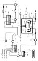
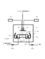
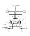
フッ酸噴出ノズル36から噴出するフッ酸溶液(HF)は、高温(例えば、160℃程度)の使用済みエッチング液LETCが溜められて高温環境となる内側液溜めカップ33cに、霧状に、あるいは、その高温環境によって一部または全部が蒸気になって与えられる。内側液溜めカップ33cでは、使用済みエッチング液LETC(リン酸アンモニウム([NH4 +]3[PO4 3-])及び二水素ケイ酸(H2SiO3)を含む)とフッ酸溶液(HF)とが所定の高温環境のもとで混合して反応し、フッ化物成分が気散(気体状になって発散する)してリン酸(H3PO4)が溶液として再生される。
11 ヒータユニット
12 リン酸供給部
13 水供給部
14 シリカ供給部
15 ポンプ
16 切替え弁
17 濃度検出器
20 エッチング液貯留槽
21 ヒータユニット
22a、22b 開閉弁
23 ポンプ
24 流量計
25 切替え弁
26 冷却器
30 スピン処理ユニット
31 処理室
32 基板スピン機構
33 セパレートカップ機構
34 エッチング液噴出ノズル
35 リンス液噴出ノズル
36 フッ酸噴出ノズル
37a、37b 開閉弁
38 ポンプ
41 リンス液供給部
42 フッ酸供給部
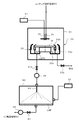
50 リン酸回収槽
51 ヒータユニット
52 ポンプ
60 再生処理槽
61 開閉弁
62 ポンプ
63 使用済みエッチング液噴出ノズル
64 フッ酸噴出ノズル
70 バッチ処理槽
71 ヒータユニット
80 再生処理槽
81 使用済みエッチング液噴出ノズル
82 フッ酸噴出ノズル
84 フッ酸供給部
86a、86b 開閉弁
Claims (8)
- 基板を回転させる基板スピン機構と、前記基板スピン機構によって回転される前記基板の表面にエッチング液を供給するエッチング液供給機構と、前記回転する基板の表面に供給される前記エッチング液が前記基板の表面から飛散した後の使用済みエッチング液を溜める液溜め部と、を有するエッチング処理部を用いて、窒化膜が形成されたシリコン製の基板をリン酸を含むエッチング液により処理する基板処理方法であって、
1枚ずつ供給される前記基板のそれぞれを前記基板スピン機構で回転させ、前記回転する前記基板に前記エッチング液供給機構から前記エッチング液を供給して前記基板に対するエッチング処理を行い、窒化膜を除去するエッチング処理ステップと、
前記エッチング処理ステップにて1枚ずつ所定枚数の前記基板を処理した分の使用済みエッチング液と、フッ酸溶液とを、前記液溜め部にて混合してリン酸を再生するリン酸再生ステップと、
前記リン酸再生ステップにより得られたリン酸を前記エッチング処理ステップにて使用されるべきエッチング液に戻すリン酸回収ステップとを有し、
前記リン酸再生ステップは、前記使用済みエッチング液と前記フッ酸溶液とを、それらのうちの少なくともいずれか一方を霧状または蒸気状にして混合する基板処理方法。 - 前記リン酸再生ステップは、前記エッチング処理ステップにて1枚の前記基板を処理した分の使用済みエッチング液と、前記フッ酸溶液とを混合してリン酸を再生する請求項1記載の基板処理方法。
- 前記リン酸再生ステップは、前記液溜め部に溜まった使用済みエッチング液に、前記フッ酸溶液を供給する請求項1または請求項2に記載の基板処理方法。
- 前記リン酸再生ステップは、前記液溜め部に予め溜められたフッ酸溶液に、前記回転する基板の表面に供給されるエッチング液が前記基板の表面から飛散した後の使用済みエッチング液を与える請求項1または請求項2に記載の基板処理方法。
- 窒化膜が形成されたシリコン製の基板をリン酸を含むエッチング液により処理する基板処理装置であって、
1枚ずつ供給される基板のそれぞれを回転させる基板スピン機構と、前記基板スピン機構によって回転される前記基板の表面に前記エッチング液を供給するエッチング液供給機構と、前記回転する基板の表面に供給される前記エッチング液が前記基板の表面から飛散した後の使用済みエッチング液を溜める液溜め部とを有し、前記基板に前記エッチング液を供給して前記基板に対するエッチング処理を行い、窒化膜を除去するエッチング処理部と、
前記液溜め部にフッ酸溶液を供給するフッ酸供給機構を有し、前記使用済みエッチング液と、前記フッ酸溶液とを、前記液溜め部にて混合してリン酸を再生するリン酸再生部と、
前記リン酸再生部により得られたリン酸を前記エッチング処理部にて使用されるべきエッチング液に戻すリン酸回収部と、
を有し、
前記リン酸再生部は、前記使用済みエッチング液と前記フッ酸溶液とを、それらのうちの少なくともいずれか一方を霧状または蒸気状にして混合する基板処理装置。 - 前記リン酸再生部は、前記エッチング処理部にて1枚の前記基板を処理した分の使用済みエッチング液と、前記フッ酸溶液とを混合してリン酸を再生する請求項5記載の基板処理装置。
- 前記フッ酸供給機構は、前記液溜め部に溜まった使用済みエッチング液に、前記フッ酸溶液を供給する請求項5または請求項6に記載の基板処理装置。
- 前記リン酸再生部は、前記フッ酸供給機構によって前記液溜め部に予め溜められたフッ酸溶液に、前記回転する基板の表面に与えられるエッチング液が前記基板の表面から飛散した後の使用済みエッチング液を与える請求項5または6に記載の基板処理装置。
Priority Applications (7)
| Application Number | Priority Date | Filing Date | Title |
|---|---|---|---|
| JP2014170205A JP6502633B2 (ja) | 2013-09-30 | 2014-08-25 | 基板処理方法及び基板処理装置 |
| TW103130267A TWI539516B (zh) | 2013-09-30 | 2014-09-02 | 基板處理方法及基板處理裝置 |
| US14/490,939 US10319602B2 (en) | 2013-09-30 | 2014-09-19 | Substrate treatment method and substrate treatment apparatus |
| CN201410504744.7A CN104517827B (zh) | 2013-09-30 | 2014-09-26 | 基板处理方法和基板处理装置 |
| CN201710432802.3A CN107256842B (zh) | 2013-09-30 | 2014-09-26 | 基板处理方法和基板处理装置 |
| KR20140130302A KR20150037632A (ko) | 2013-09-30 | 2014-09-29 | 기판 처리 방법 및 기판 처리 장치 |
| KR1020170027025A KR102129450B1 (ko) | 2013-09-30 | 2017-03-02 | 기판 처리 방법 및 기판 처리 장치 |
Applications Claiming Priority (5)
| Application Number | Priority Date | Filing Date | Title |
|---|---|---|---|
| JP2013205624 | 2013-09-30 | ||
| JP2013205624 | 2013-09-30 | ||
| JP2013259658 | 2013-12-16 | ||
| JP2013259658 | 2013-12-16 | ||
| JP2014170205A JP6502633B2 (ja) | 2013-09-30 | 2014-08-25 | 基板処理方法及び基板処理装置 |
Related Child Applications (1)
| Application Number | Title | Priority Date | Filing Date |
|---|---|---|---|
| JP2017158528A Division JP6352511B2 (ja) | 2013-09-30 | 2017-08-21 | 基板処理装置 |
Publications (3)
| Publication Number | Publication Date |
|---|---|
| JP2015135943A JP2015135943A (ja) | 2015-07-27 |
| JP2015135943A5 JP2015135943A5 (ja) | 2017-10-05 |
| JP6502633B2 true JP6502633B2 (ja) | 2019-04-17 |
Family
ID=52740578
Family Applications (1)
| Application Number | Title | Priority Date | Filing Date |
|---|---|---|---|
| JP2014170205A Active JP6502633B2 (ja) | 2013-09-30 | 2014-08-25 | 基板処理方法及び基板処理装置 |
Country Status (5)
| Country | Link |
|---|---|
| US (1) | US10319602B2 (ja) |
| JP (1) | JP6502633B2 (ja) |
| KR (2) | KR20150037632A (ja) |
| CN (2) | CN107256842B (ja) |
| TW (1) | TWI539516B (ja) |
Families Citing this family (46)
| Publication number | Priority date | Publication date | Assignee | Title |
|---|---|---|---|---|
| KR102057220B1 (ko) * | 2013-02-19 | 2020-01-22 | 삼성전자주식회사 | 약액 공급기, 약액 공급기를 구비하는 기판 처리 장치 및 이를 이용한 기판의 처리방법 |
| JP6502633B2 (ja) * | 2013-09-30 | 2019-04-17 | 芝浦メカトロニクス株式会社 | 基板処理方法及び基板処理装置 |
| DE102013220810A1 (de) * | 2013-10-15 | 2015-04-16 | Robert Bosch Gmbh | Vorrichtung zur homogenen nasschemischen Behandlung von Substraten |
| KR101671118B1 (ko) | 2014-07-29 | 2016-10-31 | 가부시키가이샤 스크린 홀딩스 | 기판 처리 장치 및 기판 처리 방법 |
| JP6320869B2 (ja) * | 2014-07-29 | 2018-05-09 | 株式会社Screenホールディングス | 基板処理装置および基板処理方法 |
| JP6359925B2 (ja) | 2014-09-18 | 2018-07-18 | 株式会社Screenホールディングス | 基板処理装置 |
| JP6383254B2 (ja) * | 2014-11-04 | 2018-08-29 | 株式会社東芝 | 処理装置および処理方法 |
| US10283384B2 (en) | 2015-04-27 | 2019-05-07 | Taiwan Semiconductor Manufacturing Co., Ltd. | Method for etching etch layer and wafer etching apparatus |
| KR101757812B1 (ko) | 2015-05-29 | 2017-07-14 | 세메스 주식회사 | 인산 재생 유닛 및 방법, 그리고 기판 처리 장치 및 방법 |
| CN105065914A (zh) * | 2015-07-21 | 2015-11-18 | 武汉新芯集成电路制造有限公司 | 一种湿法刻蚀工艺中刻蚀液输送管路系统及输送方法 |
| KR101962080B1 (ko) * | 2015-09-30 | 2019-03-25 | 시바우라 메카트로닉스 가부시끼가이샤 | 기판 처리 장치 및 기판 처리 방법 |
| KR102498830B1 (ko) * | 2015-12-29 | 2023-02-10 | 솔브레인 주식회사 | 식각액의 정제 방법 |
| JP6861039B2 (ja) * | 2016-03-30 | 2021-04-21 | 芝浦メカトロニクス株式会社 | 基板処理装置及び基板処理方法 |
| US10325779B2 (en) * | 2016-03-30 | 2019-06-18 | Tokyo Electron Limited | Colloidal silica growth inhibitor and associated method and system |
| TWI738757B (zh) * | 2016-04-05 | 2021-09-11 | 美商維克儀器公司 | 經由化學的適應性峰化來控制蝕刻速率的裝置和方法 |
| KR101870650B1 (ko) * | 2016-08-25 | 2018-06-27 | 세메스 주식회사 | 기판 처리 장치 및 기판 처리 방법 |
| CN106783692B (zh) * | 2017-01-12 | 2018-01-12 | 广东工业大学 | 一种微结构刻蚀的加工装置 |
| JP6909620B2 (ja) * | 2017-04-20 | 2021-07-28 | 株式会社Screenホールディングス | 基板処理方法 |
| JP6777704B2 (ja) * | 2017-10-20 | 2020-10-28 | 東京エレクトロン株式会社 | 基板処理装置、基板処理方法および記憶媒体 |
| KR102264002B1 (ko) | 2017-10-20 | 2021-06-11 | 도쿄엘렉트론가부시키가이샤 | 기판 처리 장치, 기판 처리 방법 및 기억 매체 |
| JP7004144B2 (ja) * | 2017-10-25 | 2022-01-21 | 株式会社Screenホールディングス | 基板処理装置および基板処理方法 |
| JP6917868B2 (ja) * | 2017-11-15 | 2021-08-11 | 株式会社Screenホールディングス | 基板処理方法および基板処理装置 |
| KR102495512B1 (ko) * | 2017-12-26 | 2023-02-06 | 솔브레인 주식회사 | 식각용 조성물 및 이를 이용한 반도체 소자의 제조방법 |
| JP6976166B2 (ja) * | 2017-12-28 | 2021-12-08 | 東京エレクトロン株式会社 | 基板処理方法および基板処理装置 |
| CN108109946A (zh) * | 2018-01-16 | 2018-06-01 | 昆山成功环保科技有限公司 | 一种刻蚀设备 |
| JP7045199B2 (ja) | 2018-01-23 | 2022-03-31 | 株式会社Screenホールディングス | 基板処理装置および基板処理方法 |
| KR20190099814A (ko) * | 2018-02-20 | 2019-08-28 | 삼성전자주식회사 | 약액 리사이클 시스템, 약액 공급 시스템 및 이를 이용한 반도체 장치 제조 방법 |
| JP2020035794A (ja) * | 2018-08-27 | 2020-03-05 | キオクシア株式会社 | 基板処理装置および半導体装置の製造方法 |
| CN109037119B (zh) * | 2018-09-13 | 2021-04-09 | 友达光电(昆山)有限公司 | 一种蚀刻装置 |
| JP7096112B2 (ja) | 2018-09-13 | 2022-07-05 | キオクシア株式会社 | 半導体製造装置および半導体装置の製造方法 |
| JP7158249B2 (ja) * | 2018-11-09 | 2022-10-21 | 東京エレクトロン株式会社 | 基板処理方法、基板処理装置および記憶媒体 |
| JP7126927B2 (ja) * | 2018-11-16 | 2022-08-29 | 株式会社Screenホールディングス | 基板処理装置および基板処理方法 |
| JP7203579B2 (ja) * | 2018-11-26 | 2023-01-13 | 株式会社Screenホールディングス | 基板処理装置 |
| JP7190892B2 (ja) * | 2018-12-12 | 2022-12-16 | 東京エレクトロン株式会社 | 基板処理装置および処理液濃縮方法 |
| CN109698148B (zh) * | 2018-12-27 | 2021-04-13 | 上海华力集成电路制造有限公司 | 一种用于磷酸机台温度控制的管路设备 |
| JP2020141006A (ja) * | 2019-02-27 | 2020-09-03 | キオクシア株式会社 | 基板処理装置および半導体装置の製造方法 |
| CN111696891B (zh) * | 2019-03-15 | 2024-05-03 | 东京毅力科创株式会社 | 基片处理装置、混合方法和基片处理方法 |
| KR102346529B1 (ko) * | 2019-06-24 | 2021-12-31 | 세메스 주식회사 | 액 공급 유닛, 그리고 이를 가지는 기판 처리 장치 및 방법 |
| JP7391297B2 (ja) * | 2019-06-28 | 2023-12-05 | 株式会社Flosfia | エッチング処理方法およびエッチング処理装置 |
| CN111106041A (zh) * | 2019-12-10 | 2020-05-05 | 上海华力集成电路制造有限公司 | 湿法刻蚀机台及湿法刻蚀药液的回收方法 |
| CN111354637B (zh) * | 2020-02-28 | 2023-07-25 | 通威太阳能(眉山)有限公司 | 一种氢氟酸循环利用洗石墨舟的方法 |
| JP7413113B2 (ja) | 2020-03-24 | 2024-01-15 | 株式会社Screenホールディングス | 処理液温調方法、基板処理方法、処理液温調装置、及び、基板処理システム |
| JP7467279B2 (ja) * | 2020-08-18 | 2024-04-15 | キオクシア株式会社 | 薬液塗布装置および粘度調整ボトル |
| KR20220088561A (ko) * | 2020-12-18 | 2022-06-28 | 세메스 주식회사 | 처리액 공급 장치 및 처리액 공급 방법 |
| JP7438172B2 (ja) | 2021-09-13 | 2024-02-26 | 芝浦メカトロニクス株式会社 | 供給装置、供給システム |
| CN113943579A (zh) * | 2021-10-15 | 2022-01-18 | 中国科学院上海微系统与信息技术研究所 | 组合型刻蚀液、刻蚀系统及刻蚀方法 |
Family Cites Families (15)
| Publication number | Priority date | Publication date | Assignee | Title |
|---|---|---|---|---|
| JPH04288831A (ja) * | 1991-03-18 | 1992-10-13 | Nec Yamagata Ltd | 半導体製造装置 |
| US6086711A (en) * | 1997-10-06 | 2000-07-11 | Nisene Technology Group | Vapor generation system and process |
| US6399517B2 (en) * | 1999-03-30 | 2002-06-04 | Tokyo Electron Limited | Etching method and etching apparatus |
| JP2003215002A (ja) * | 2002-01-17 | 2003-07-30 | Dainippon Screen Mfg Co Ltd | 基板処理装置および基板処理方法 |
| JP2005064199A (ja) * | 2003-08-11 | 2005-03-10 | Seiko Epson Corp | 薬液再生処理装置、半導体製造装置、薬液再生処理方法および半導体装置の製造方法 |
| JP2005079212A (ja) | 2003-08-29 | 2005-03-24 | Trecenti Technologies Inc | 半導体製造装置、及び半導体装置の製造方法 |
| TWI334624B (en) * | 2006-01-30 | 2010-12-11 | Dainippon Screen Mfg | Apparatus for and method for processing substrate |
| JP2008066351A (ja) * | 2006-09-05 | 2008-03-21 | Dainippon Screen Mfg Co Ltd | 基板処理装置 |
| JP4944558B2 (ja) * | 2006-10-12 | 2012-06-06 | アプリシアテクノロジー株式会社 | エッチング液の再生方法、エッチング方法およびエッチング装置 |
| JP4412502B2 (ja) * | 2007-02-14 | 2010-02-10 | セイコーエプソン株式会社 | 処理装置および半導体装置の製造方法 |
| JP4424517B2 (ja) * | 2007-02-19 | 2010-03-03 | セイコーエプソン株式会社 | 処理装置および半導体装置の製造方法 |
| JP4358259B2 (ja) * | 2007-06-05 | 2009-11-04 | 株式会社東芝 | 半導体製造装置および半導体製造方法 |
| KR101592058B1 (ko) * | 2010-06-03 | 2016-02-05 | 도쿄엘렉트론가부시키가이샤 | 기판 액처리 장치 |
| JP2012074601A (ja) * | 2010-09-29 | 2012-04-12 | Dainippon Screen Mfg Co Ltd | 基板処理装置および基板処理方法 |
| JP6502633B2 (ja) * | 2013-09-30 | 2019-04-17 | 芝浦メカトロニクス株式会社 | 基板処理方法及び基板処理装置 |
-
2014
- 2014-08-25 JP JP2014170205A patent/JP6502633B2/ja active Active
- 2014-09-02 TW TW103130267A patent/TWI539516B/zh active
- 2014-09-19 US US14/490,939 patent/US10319602B2/en active Active
- 2014-09-26 CN CN201710432802.3A patent/CN107256842B/zh active Active
- 2014-09-26 CN CN201410504744.7A patent/CN104517827B/zh active Active
- 2014-09-29 KR KR20140130302A patent/KR20150037632A/ko active Application Filing
-
2017
- 2017-03-02 KR KR1020170027025A patent/KR102129450B1/ko active IP Right Grant
Also Published As
| Publication number | Publication date |
|---|---|
| CN107256842A (zh) | 2017-10-17 |
| TW201530646A (zh) | 2015-08-01 |
| US10319602B2 (en) | 2019-06-11 |
| US20150093906A1 (en) | 2015-04-02 |
| CN107256842B (zh) | 2021-06-04 |
| KR20170029453A (ko) | 2017-03-15 |
| KR20150037632A (ko) | 2015-04-08 |
| CN104517827A (zh) | 2015-04-15 |
| TWI539516B (zh) | 2016-06-21 |
| JP2015135943A (ja) | 2015-07-27 |
| CN104517827B (zh) | 2017-06-27 |
| KR102129450B1 (ko) | 2020-07-03 |
Similar Documents
| Publication | Publication Date | Title |
|---|---|---|
| JP6502633B2 (ja) | 基板処理方法及び基板処理装置 | |
| JP2015135943A5 (ja) | ||
| JP6352511B2 (ja) | 基板処理装置 | |
| KR102541745B1 (ko) | 습식 에칭 방법, 기판 액처리 장치 및 기억 매체 | |
| JP5715981B2 (ja) | 基板処理方法および基板処理装置 | |
| JP6066899B2 (ja) | 基板表面の近傍における流体の混合制御による超小型電子基板の湿式処理 | |
| CN103153490A (zh) | 用于干燥半导体晶片的方法和装置 | |
| CN103348452A (zh) | 用于从衬底选择性地移除氮化物的方法 | |
| US20170062231A1 (en) | Substrate treatment apparatus, substrate treatment method, and etchant | |
| KR20130121033A (ko) | 기판 처리 장치 및 기판 처리 방법 | |
| US20130276822A1 (en) | Hyperbaric methods and systems for rinsing and drying granular materials | |
| KR20180054598A (ko) | 기판 처리 방법, 기판 처리 장치 및 기억 매체 | |
| US10290491B2 (en) | Substrate treatment apparatus and substrate treatment method | |
| US20190385869A1 (en) | Substrate processing apparatus and processing liquid reuse method | |
| KR102003361B1 (ko) | 인시튜 건식 세정 방법 및 장치 | |
| CN101406888B (zh) | 用于供应化学液体的装置 | |
| JP2007273806A (ja) | 半導体基板の洗浄方法および洗浄装置 | |
| US11745213B2 (en) | Substrate processing apparatus and apparatus cleaning method | |
| US20210118704A1 (en) | Substrate processing apparatus and apparatus cleaning method | |
| JP5961535B2 (ja) | 基板液処理方法、基板液処理システムおよび記憶媒体 | |
| JP7065622B2 (ja) | 基板処理装置及び基板処理方法 | |
| JP4227694B2 (ja) | ウエハーの表面処理装置 | |
| KR20040032200A (ko) | 반도체 웨이퍼 세정 및 건조장치와 이를 이용한 세정 및건조방법 | |
| TW202220027A (zh) | 基板處理方法及基板處理裝置 | |
| US20080163891A1 (en) | Method and apparatus of multi steps atomization for generating smaller diw dropplets for wafer cleaning |
Legal Events
| Date | Code | Title | Description |
|---|---|---|---|
| A521 | Written amendment |
Free format text: JAPANESE INTERMEDIATE CODE: A523 Effective date: 20170821 |
|
| A621 | Written request for application examination |
Free format text: JAPANESE INTERMEDIATE CODE: A621 Effective date: 20170821 |
|
| A977 | Report on retrieval |
Free format text: JAPANESE INTERMEDIATE CODE: A971007 Effective date: 20180525 |
|
| A131 | Notification of reasons for refusal |
Free format text: JAPANESE INTERMEDIATE CODE: A131 Effective date: 20180605 |
|
| A601 | Written request for extension of time |
Free format text: JAPANESE INTERMEDIATE CODE: A601 Effective date: 20180803 |
|
| A521 | Written amendment |
Free format text: JAPANESE INTERMEDIATE CODE: A523 Effective date: 20181004 |
|
| TRDD | Decision of grant or rejection written | ||
| A01 | Written decision to grant a patent or to grant a registration (utility model) |
Free format text: JAPANESE INTERMEDIATE CODE: A01 Effective date: 20190319 |
|
| A61 | First payment of annual fees (during grant procedure) |
Free format text: JAPANESE INTERMEDIATE CODE: A61 Effective date: 20190322 |
|
| R150 | Certificate of patent or registration of utility model |
Ref document number: 6502633 Country of ref document: JP Free format text: JAPANESE INTERMEDIATE CODE: R150 |