JP6377975B2 - 基板固定装置 - Google Patents
基板固定装置 Download PDFInfo
- Publication number
- JP6377975B2 JP6377975B2 JP2014128275A JP2014128275A JP6377975B2 JP 6377975 B2 JP6377975 B2 JP 6377975B2 JP 2014128275 A JP2014128275 A JP 2014128275A JP 2014128275 A JP2014128275 A JP 2014128275A JP 6377975 B2 JP6377975 B2 JP 6377975B2
- Authority
- JP
- Japan
- Prior art keywords
- electrostatic
- electrode
- base
- substrate
- tray
- Prior art date
- Legal status (The legal status is an assumption and is not a legal conclusion. Google has not performed a legal analysis and makes no representation as to the accuracy of the status listed.)
- Active
Links
Images


Classifications
-
- H—ELECTRICITY
- H01—ELECTRIC ELEMENTS
- H01L—SEMICONDUCTOR DEVICES NOT COVERED BY CLASS H10
- H01L21/00—Processes or apparatus adapted for the manufacture or treatment of semiconductor or solid state devices or of parts thereof
- H01L21/67—Apparatus specially adapted for handling semiconductor or electric solid state devices during manufacture or treatment thereof; Apparatus specially adapted for handling wafers during manufacture or treatment of semiconductor or electric solid state devices or components ; Apparatus not specifically provided for elsewhere
- H01L21/683—Apparatus specially adapted for handling semiconductor or electric solid state devices during manufacture or treatment thereof; Apparatus specially adapted for handling wafers during manufacture or treatment of semiconductor or electric solid state devices or components ; Apparatus not specifically provided for elsewhere for supporting or gripping
- H01L21/6831—Apparatus specially adapted for handling semiconductor or electric solid state devices during manufacture or treatment thereof; Apparatus specially adapted for handling wafers during manufacture or treatment of semiconductor or electric solid state devices or components ; Apparatus not specifically provided for elsewhere for supporting or gripping using electrostatic chucks
- H01L21/6833—Details of electrostatic chucks
-
- H—ELECTRICITY
- H01—ELECTRIC ELEMENTS
- H01L—SEMICONDUCTOR DEVICES NOT COVERED BY CLASS H10
- H01L21/00—Processes or apparatus adapted for the manufacture or treatment of semiconductor or solid state devices or of parts thereof
- H01L21/67—Apparatus specially adapted for handling semiconductor or electric solid state devices during manufacture or treatment thereof; Apparatus specially adapted for handling wafers during manufacture or treatment of semiconductor or electric solid state devices or components ; Apparatus not specifically provided for elsewhere
- H01L21/67005—Apparatus not specifically provided for elsewhere
- H01L21/67011—Apparatus for manufacture or treatment
- H01L21/67098—Apparatus for thermal treatment
- H01L21/67109—Apparatus for thermal treatment mainly by convection
-
- H—ELECTRICITY
- H01—ELECTRIC ELEMENTS
- H01L—SEMICONDUCTOR DEVICES NOT COVERED BY CLASS H10
- H01L21/00—Processes or apparatus adapted for the manufacture or treatment of semiconductor or solid state devices or of parts thereof
- H01L21/67—Apparatus specially adapted for handling semiconductor or electric solid state devices during manufacture or treatment thereof; Apparatus specially adapted for handling wafers during manufacture or treatment of semiconductor or electric solid state devices or components ; Apparatus not specifically provided for elsewhere
- H01L21/683—Apparatus specially adapted for handling semiconductor or electric solid state devices during manufacture or treatment thereof; Apparatus specially adapted for handling wafers during manufacture or treatment of semiconductor or electric solid state devices or components ; Apparatus not specifically provided for elsewhere for supporting or gripping
- H01L21/687—Apparatus specially adapted for handling semiconductor or electric solid state devices during manufacture or treatment thereof; Apparatus specially adapted for handling wafers during manufacture or treatment of semiconductor or electric solid state devices or components ; Apparatus not specifically provided for elsewhere for supporting or gripping using mechanical means, e.g. chucks, clamps or pinches
- H01L21/68714—Apparatus specially adapted for handling semiconductor or electric solid state devices during manufacture or treatment thereof; Apparatus specially adapted for handling wafers during manufacture or treatment of semiconductor or electric solid state devices or components ; Apparatus not specifically provided for elsewhere for supporting or gripping using mechanical means, e.g. chucks, clamps or pinches the wafers being placed on a susceptor, stage or support
- H01L21/6875—Apparatus specially adapted for handling semiconductor or electric solid state devices during manufacture or treatment thereof; Apparatus specially adapted for handling wafers during manufacture or treatment of semiconductor or electric solid state devices or components ; Apparatus not specifically provided for elsewhere for supporting or gripping using mechanical means, e.g. chucks, clamps or pinches the wafers being placed on a susceptor, stage or support characterised by a plurality of individual support members, e.g. support posts or protrusions
-
- H—ELECTRICITY
- H01—ELECTRIC ELEMENTS
- H01L—SEMICONDUCTOR DEVICES NOT COVERED BY CLASS H10
- H01L21/00—Processes or apparatus adapted for the manufacture or treatment of semiconductor or solid state devices or of parts thereof
- H01L21/67—Apparatus specially adapted for handling semiconductor or electric solid state devices during manufacture or treatment thereof; Apparatus specially adapted for handling wafers during manufacture or treatment of semiconductor or electric solid state devices or components ; Apparatus not specifically provided for elsewhere
- H01L21/683—Apparatus specially adapted for handling semiconductor or electric solid state devices during manufacture or treatment thereof; Apparatus specially adapted for handling wafers during manufacture or treatment of semiconductor or electric solid state devices or components ; Apparatus not specifically provided for elsewhere for supporting or gripping
- H01L21/687—Apparatus specially adapted for handling semiconductor or electric solid state devices during manufacture or treatment thereof; Apparatus specially adapted for handling wafers during manufacture or treatment of semiconductor or electric solid state devices or components ; Apparatus not specifically provided for elsewhere for supporting or gripping using mechanical means, e.g. chucks, clamps or pinches
- H01L21/68714—Apparatus specially adapted for handling semiconductor or electric solid state devices during manufacture or treatment thereof; Apparatus specially adapted for handling wafers during manufacture or treatment of semiconductor or electric solid state devices or components ; Apparatus not specifically provided for elsewhere for supporting or gripping using mechanical means, e.g. chucks, clamps or pinches the wafers being placed on a susceptor, stage or support
- H01L21/68771—Apparatus specially adapted for handling semiconductor or electric solid state devices during manufacture or treatment thereof; Apparatus specially adapted for handling wafers during manufacture or treatment of semiconductor or electric solid state devices or components ; Apparatus not specifically provided for elsewhere for supporting or gripping using mechanical means, e.g. chucks, clamps or pinches the wafers being placed on a susceptor, stage or support characterised by supporting more than one semiconductor substrate
Description
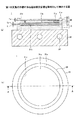
図1は、第1の実施の形態に係る基板固定装置を簡略化して例示する図であり、図1(b)が平面図、図1(a)は図1(b)のA−A線に沿う断面図である。図1を参照するに、基板固定装置1は、大略すると、静電チャック10と、ベースプレート20と、静電吸着用トレイ30とを有する。
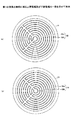
第1の実施の形態の変形例1では、上層電極を複数個有し、載置面の上層電極に対応する位置に複数の吸着対象物を載置可能な基板固定装置の例を示す。なお、第1の実施の形態の変形例1において、既に説明した実施の形態と同一構成部品についての説明は省略する場合がある。
第1の実施の形態の変形例2では、冷却効率を向上可能な静電吸着用トレイを搭載した基板固定装置の例を示す。なお、第1の実施の形態の変形例2において、既に説明した実施の形態と同一構成部品についての説明は省略する場合がある。
10 静電チャック
11、31 基体
11a、31a 上面
12 静電電極
20 ベースプレート
21 冷却水路
30、30A、30B 静電吸着用トレイ
31b 背面
31c 載置面
31d 堰部
31e 突起部
31f 貫通孔
31x、31y 凹部
32、35 上層電極
33 下層電極
34 配線
100、110 吸着対象物
Claims (6)
- 吸着対象物が載置される載置面、及び前記載置面の反対面となる背面を備えた第1基体と、
前記第1基体の前記載置面側に内蔵された上層電極と、
前記第1基体の前記上層電極よりも前記背面側に内蔵された下層電極と、
前記上層電極と前記下層電極とを電気的に接続する配線と、
前記第1基体の背面側に設けられた不活性ガスを充填させる空間と、を有し、
前記上層電極及び前記下層電極は、前記第1基体に完全に包囲され、前記第1基体の外部に露出する部分がなく、
前記載置面は前記第1基体の上面に設けられた凹部の底面であり、
前記背面側から与えられる静電位により、前記載置面に載置される前記吸着対象物を保持する静電吸着用トレイと、
静電電極が内蔵された第2基体を備えた静電チャックと、を有し、
前記静電電極と前記下層電極とは対向するように配され、
前記静電吸着用トレイは、前記第2基体の上面に着脱可能な状態で載置され、
前記第1基体及び前記第2基体は低抵抗誘電体から構成されている基板固定装置。 - 前記載置面及び前記背面は何れも研磨された面である請求項1記載の基板固定装置。
- 前記載置面及び前記上層電極を複数個有し、
夫々の前記載置面は、前記第1基体の上面の、夫々の前記上層電極に対応する位置に設けられた凹部の底面であり、
夫々の前記載置面に吸着対象物を載置可能な請求項1又は2記載の基板固定装置。 - 前記載置面に吸着対象物が載置され、前記静電電極に電圧が印加されると、前記下層電極が前記静電電極に吸着されて前記静電吸着用トレイが前記第2基体の上面に保持され、前記吸着対象物が前記上層電極に吸着されて前記吸着対象物が前記載置面に保持される請求項1乃至3の何れか一項記載の基板固定装置。
- 前記第2基体の上面は研磨された面である請求項1乃至4の何れか一項記載の基板固定装置。
- 前記静電チャックは、前記静電吸着用トレイに不活性ガスを供給するガス路を備えている請求項1乃至5の何れか一項記載の基板固定装置。
Priority Applications (4)
| Application Number | Priority Date | Filing Date | Title |
|---|---|---|---|
| JP2014128275A JP6377975B2 (ja) | 2014-06-23 | 2014-06-23 | 基板固定装置 |
| US14/732,868 US9837297B2 (en) | 2014-06-23 | 2015-06-08 | Tray and wafer holding apparatus |
| TW104118706A TWI640054B (zh) | 2014-06-23 | 2015-06-10 | 托盤及晶圓固持裝置 |
| KR1020150084935A KR102266688B1 (ko) | 2014-06-23 | 2015-06-16 | 트레이 및 웨이퍼 고정 장치 |
Applications Claiming Priority (1)
| Application Number | Priority Date | Filing Date | Title |
|---|---|---|---|
| JP2014128275A JP6377975B2 (ja) | 2014-06-23 | 2014-06-23 | 基板固定装置 |
Publications (3)
| Publication Number | Publication Date |
|---|---|
| JP2016009715A JP2016009715A (ja) | 2016-01-18 |
| JP2016009715A5 JP2016009715A5 (ja) | 2017-02-23 |
| JP6377975B2 true JP6377975B2 (ja) | 2018-08-22 |
Family
ID=54870313
Family Applications (1)
| Application Number | Title | Priority Date | Filing Date |
|---|---|---|---|
| JP2014128275A Active JP6377975B2 (ja) | 2014-06-23 | 2014-06-23 | 基板固定装置 |
Country Status (4)
| Country | Link |
|---|---|
| US (1) | US9837297B2 (ja) |
| JP (1) | JP6377975B2 (ja) |
| KR (1) | KR102266688B1 (ja) |
| TW (1) | TWI640054B (ja) |
Families Citing this family (14)
| Publication number | Priority date | Publication date | Assignee | Title |
|---|---|---|---|---|
| JP6010720B1 (ja) * | 2015-01-20 | 2016-10-19 | 日本碍子株式会社 | ウエハ支持構造体 |
| US11532497B2 (en) * | 2016-06-07 | 2022-12-20 | Applied Materials, Inc. | High power electrostatic chuck design with radio frequency coupling |
| US10770270B2 (en) * | 2016-06-07 | 2020-09-08 | Applied Materials, Inc. | High power electrostatic chuck with aperture-reducing plug in a gas hole |
| US20180096867A1 (en) * | 2016-09-30 | 2018-04-05 | Momentive Performance Materials Inc. | Heating apparatus with controlled thermal contact |
| US20190249294A1 (en) * | 2016-11-07 | 2019-08-15 | Applied Materials, Inc. | Carrier for holding a substrate, use of the carrier in a processing system, processing system employing the carrier, and method for controlling a temperature of a substrate |
| JP6986937B2 (ja) * | 2017-01-05 | 2021-12-22 | 東京エレクトロン株式会社 | プラズマ処理装置 |
| JP6858035B2 (ja) * | 2017-02-27 | 2021-04-14 | 新光電気工業株式会社 | 基板固定具及び基板固定装置 |
| JP6969182B2 (ja) * | 2017-07-06 | 2021-11-24 | 東京エレクトロン株式会社 | プラズマ処理装置 |
| US20190105748A1 (en) * | 2017-10-11 | 2019-04-11 | Samsung Electronics Co., Ltd. | Seal-less airlock wafer stage |
| JP7049108B2 (ja) * | 2017-12-25 | 2022-04-06 | 日本特殊陶業株式会社 | 静電チャック |
| DE102018127658A1 (de) * | 2018-11-06 | 2020-05-07 | Asm Assembly Systems Gmbh & Co. Kg | Elektrostatisches Aufspannen von Elektronikplatten |
| CN113574652B (zh) * | 2019-03-18 | 2023-09-01 | 日本碍子株式会社 | 静电卡盘 |
| JP7386086B2 (ja) | 2020-01-07 | 2023-11-24 | 日本特殊陶業株式会社 | 保持装置 |
| US20230215704A1 (en) * | 2020-06-29 | 2023-07-06 | Sumitomo Osaka Cement Co., Ltd. | Electrostatic chuck device |
Family Cites Families (16)
| Publication number | Priority date | Publication date | Assignee | Title |
|---|---|---|---|---|
| JP2767282B2 (ja) * | 1989-05-30 | 1998-06-18 | 日本真空技術株式会社 | 基板保持装置 |
| JPH05259048A (ja) * | 1992-03-09 | 1993-10-08 | Nippon Telegr & Teleph Corp <Ntt> | 試料加工用装置、試料搬送用装置及び試料搬送・加工用装置 |
| JP3596127B2 (ja) * | 1995-12-04 | 2004-12-02 | ソニー株式会社 | 静電チャック、薄板保持装置、半導体製造装置、搬送方法及び半導体の製造方法 |
| JP4256503B2 (ja) * | 1997-10-30 | 2009-04-22 | 東京エレクトロン株式会社 | 真空処理装置 |
| JP4346877B2 (ja) * | 2002-08-29 | 2009-10-21 | 東京エレクトロン株式会社 | 静電吸着装置および処理装置 |
| JP4302428B2 (ja) * | 2003-05-09 | 2009-07-29 | 信越化学工業株式会社 | 静電吸着機能を有するウエーハ加熱装置 |
| JP2006056731A (ja) * | 2004-08-18 | 2006-03-02 | Taiheiyo Cement Corp | 窒化アルミニウム焼結体およびそれを用いた静電チャック |
| DE102005056364B3 (de) * | 2005-11-25 | 2007-08-16 | Fraunhofer-Gesellschaft zur Förderung der angewandten Forschung e.V. | Bipolarer Trägerwafer und mobile, bipolare, elektrostatische Waferanordnung |
| JP4864757B2 (ja) * | 2007-02-14 | 2012-02-01 | 東京エレクトロン株式会社 | 基板載置台及びその表面処理方法 |
| JP2010098012A (ja) * | 2008-10-14 | 2010-04-30 | Ulvac Japan Ltd | エッチング装置及びエッチング方法 |
| JP2012074650A (ja) * | 2010-09-30 | 2012-04-12 | Samco Inc | プラズマ処理用トレイ及びプラズマ処理装置 |
| JP5638405B2 (ja) * | 2010-10-08 | 2014-12-10 | パナソニック株式会社 | 基板のプラズマ処理方法 |
| JP6285620B2 (ja) * | 2011-08-26 | 2018-02-28 | 新光電気工業株式会社 | 静電チャック及び半導体・液晶製造装置 |
| JP6122856B2 (ja) * | 2011-10-06 | 2017-04-26 | エーエスエムエル ネザーランズ ビー.ブイ. | チャック、リソグラフィ装置及びチャックを使用する方法 |
| JP6007039B2 (ja) * | 2012-09-18 | 2016-10-12 | 株式会社アルバック | 搬送トレー及び基板保持方法 |
| JP5595549B2 (ja) * | 2013-03-28 | 2014-09-24 | パナソニック株式会社 | プラズマ処理装置用トレイ、プラズマ処理装置、及びプラズマ処理方法 |
-
2014
- 2014-06-23 JP JP2014128275A patent/JP6377975B2/ja active Active
-
2015
- 2015-06-08 US US14/732,868 patent/US9837297B2/en active Active
- 2015-06-10 TW TW104118706A patent/TWI640054B/zh active
- 2015-06-16 KR KR1020150084935A patent/KR102266688B1/ko active IP Right Grant
Also Published As
| Publication number | Publication date |
|---|---|
| JP2016009715A (ja) | 2016-01-18 |
| KR20150146408A (ko) | 2015-12-31 |
| US20150371885A1 (en) | 2015-12-24 |
| TWI640054B (zh) | 2018-11-01 |
| TW201613019A (en) | 2016-04-01 |
| US9837297B2 (en) | 2017-12-05 |
| KR102266688B1 (ko) | 2021-06-21 |
Similar Documents
| Publication | Publication Date | Title |
|---|---|---|
| JP6377975B2 (ja) | 基板固定装置 | |
| JP4974873B2 (ja) | 静電チャック及び基板温調固定装置 | |
| JP6586975B2 (ja) | 静電チャック装置 | |
| US10153192B2 (en) | Electrostatic chuck device | |
| JP5250408B2 (ja) | 基板温調固定装置 | |
| JP6435247B2 (ja) | 静電チャック装置及び静電チャック装置の製造方法 | |
| JPWO2017069238A1 (ja) | 静電チャック装置 | |
| KR102233920B1 (ko) | 정전 척 장치 | |
| KR20160015510A (ko) | 정전척 어셈블리, 이를 구비하는 반도체 제조장치, 및 이를 이용한 플라즈마 처리방법 | |
| JP2009302347A (ja) | 静電チャック及び基板温調固定装置 | |
| JP2016184645A (ja) | 静電チャック装置 | |
| CN113994462A (zh) | 静电吸盘 | |
| JP6762432B2 (ja) | 保持装置 | |
| JP7296869B2 (ja) | 静電チャック、基板固定装置 | |
| JP5785862B2 (ja) | 静電チャック及びその製造方法、基板温調固定装置 | |
| JP7291046B2 (ja) | 基板固定装置 | |
| JP2010147095A (ja) | 基板固定装置 | |
| JP2021057468A (ja) | 保持装置 | |
| JP6670189B2 (ja) | ベースプレート構造体及びその製造方法、基板固定装置 | |
| JP6664790B2 (ja) | プラズマ処理装置用のトレイ | |
| KR102592338B1 (ko) | 일체형 다공성 필터를 포함하는 정전척 및 이의 제조 방법 | |
| WO2024058183A1 (ja) | 吸着基板 | |
| KR20110064665A (ko) | 전기장 구배를 이용한 쌍극형 정전척 | |
| KR102341865B1 (ko) | 수리가 용이한 정전척 | |
| TW202240757A (zh) | 靜電夾盤及基板固定裝置 |
Legal Events
| Date | Code | Title | Description |
|---|---|---|---|
| A521 | Written amendment |
Free format text: JAPANESE INTERMEDIATE CODE: A523 Effective date: 20170123 |
|
| A621 | Written request for application examination |
Free format text: JAPANESE INTERMEDIATE CODE: A621 Effective date: 20170123 |
|
| A977 | Report on retrieval |
Free format text: JAPANESE INTERMEDIATE CODE: A971007 Effective date: 20171110 |
|
| A131 | Notification of reasons for refusal |
Free format text: JAPANESE INTERMEDIATE CODE: A131 Effective date: 20171121 |
|
| A521 | Written amendment |
Free format text: JAPANESE INTERMEDIATE CODE: A523 Effective date: 20180116 |
|
| A02 | Decision of refusal |
Free format text: JAPANESE INTERMEDIATE CODE: A02 Effective date: 20180313 |
|
| A521 | Written amendment |
Free format text: JAPANESE INTERMEDIATE CODE: A523 Effective date: 20180521 |
|
| A911 | Transfer of reconsideration by examiner before appeal (zenchi) |
Free format text: JAPANESE INTERMEDIATE CODE: A911 Effective date: 20180530 |
|
| TRDD | Decision of grant or rejection written | ||
| A01 | Written decision to grant a patent or to grant a registration (utility model) |
Free format text: JAPANESE INTERMEDIATE CODE: A01 Effective date: 20180710 |
|
| A61 | First payment of annual fees (during grant procedure) |
Free format text: JAPANESE INTERMEDIATE CODE: A61 Effective date: 20180726 |
|
| R150 | Certificate of patent or registration of utility model |
Ref document number: 6377975 Country of ref document: JP Free format text: JAPANESE INTERMEDIATE CODE: R150 |