JP6355311B2 - 固体撮像装置、その製造方法及び撮像システム - Google Patents
固体撮像装置、その製造方法及び撮像システム Download PDFInfo
- Publication number
- JP6355311B2 JP6355311B2 JP2013210588A JP2013210588A JP6355311B2 JP 6355311 B2 JP6355311 B2 JP 6355311B2 JP 2013210588 A JP2013210588 A JP 2013210588A JP 2013210588 A JP2013210588 A JP 2013210588A JP 6355311 B2 JP6355311 B2 JP 6355311B2
- Authority
- JP
- Japan
- Prior art keywords
- semiconductor region
- region
- solid
- imaging device
- state imaging
- Prior art date
- Legal status (The legal status is an assumption and is not a legal conclusion. Google has not performed a legal analysis and makes no representation as to the accuracy of the status listed.)
- Active
Links
- 238000003384 imaging method Methods 0.000 title claims description 64
- 238000004519 manufacturing process Methods 0.000 title claims description 14
- 239000004065 semiconductor Substances 0.000 claims description 236
- 239000012535 impurity Substances 0.000 claims description 84
- 239000000758 substrate Substances 0.000 claims description 33
- 238000000034 method Methods 0.000 claims description 32
- 238000009826 distribution Methods 0.000 claims description 26
- 238000006243 chemical reaction Methods 0.000 claims description 25
- 238000005468 ion implantation Methods 0.000 claims description 23
- 238000005036 potential barrier Methods 0.000 claims description 8
- 230000007423 decrease Effects 0.000 claims description 7
- 238000003860 storage Methods 0.000 claims description 6
- 230000002093 peripheral effect Effects 0.000 description 7
- 238000010586 diagram Methods 0.000 description 5
- 229920002120 photoresistant polymer Polymers 0.000 description 3
- OAICVXFJPJFONN-UHFFFAOYSA-N Phosphorus Chemical compound [P] OAICVXFJPJFONN-UHFFFAOYSA-N 0.000 description 2
- 230000015572 biosynthetic process Effects 0.000 description 2
- 230000007547 defect Effects 0.000 description 2
- 238000009792 diffusion process Methods 0.000 description 2
- 239000002019 doping agent Substances 0.000 description 2
- 238000002513 implantation Methods 0.000 description 2
- 230000003071 parasitic effect Effects 0.000 description 2
- 229910052698 phosphorus Inorganic materials 0.000 description 2
- 239000011574 phosphorus Substances 0.000 description 2
- 239000012808 vapor phase Substances 0.000 description 2
- ZOXJGFHDIHLPTG-UHFFFAOYSA-N Boron Chemical compound [B] ZOXJGFHDIHLPTG-UHFFFAOYSA-N 0.000 description 1
- 102000004129 N-Type Calcium Channels Human genes 0.000 description 1
- 108090000699 N-Type Calcium Channels Proteins 0.000 description 1
- 238000009825 accumulation Methods 0.000 description 1
- 229910052785 arsenic Inorganic materials 0.000 description 1
- RQNWIZPPADIBDY-UHFFFAOYSA-N arsenic atom Chemical compound [As] RQNWIZPPADIBDY-UHFFFAOYSA-N 0.000 description 1
- 229910052796 boron Inorganic materials 0.000 description 1
- 239000013078 crystal Substances 0.000 description 1
- 230000000694 effects Effects 0.000 description 1
- 238000002955 isolation Methods 0.000 description 1
- 230000035945 sensitivity Effects 0.000 description 1
- 238000000926 separation method Methods 0.000 description 1
- 229910052710 silicon Inorganic materials 0.000 description 1
- 239000010703 silicon Substances 0.000 description 1
- 230000000087 stabilizing effect Effects 0.000 description 1
Images


Classifications
-
- H—ELECTRICITY
- H01—ELECTRIC ELEMENTS
- H01L—SEMICONDUCTOR DEVICES NOT COVERED BY CLASS H10
- H01L27/00—Devices consisting of a plurality of semiconductor or other solid-state components formed in or on a common substrate
- H01L27/14—Devices consisting of a plurality of semiconductor or other solid-state components formed in or on a common substrate including semiconductor components sensitive to infrared radiation, light, electromagnetic radiation of shorter wavelength or corpuscular radiation and specially adapted either for the conversion of the energy of such radiation into electrical energy or for the control of electrical energy by such radiation
- H01L27/144—Devices controlled by radiation
- H01L27/146—Imager structures
- H01L27/14683—Processes or apparatus peculiar to the manufacture or treatment of these devices or parts thereof
- H01L27/14689—MOS based technologies
-
- H—ELECTRICITY
- H01—ELECTRIC ELEMENTS
- H01L—SEMICONDUCTOR DEVICES NOT COVERED BY CLASS H10
- H01L27/00—Devices consisting of a plurality of semiconductor or other solid-state components formed in or on a common substrate
- H01L27/14—Devices consisting of a plurality of semiconductor or other solid-state components formed in or on a common substrate including semiconductor components sensitive to infrared radiation, light, electromagnetic radiation of shorter wavelength or corpuscular radiation and specially adapted either for the conversion of the energy of such radiation into electrical energy or for the control of electrical energy by such radiation
- H01L27/144—Devices controlled by radiation
- H01L27/146—Imager structures
- H01L27/14601—Structural or functional details thereof
- H01L27/14609—Pixel-elements with integrated switching, control, storage or amplification elements
- H01L27/1461—Pixel-elements with integrated switching, control, storage or amplification elements characterised by the photosensitive area
-
- H—ELECTRICITY
- H01—ELECTRIC ELEMENTS
- H01L—SEMICONDUCTOR DEVICES NOT COVERED BY CLASS H10
- H01L27/00—Devices consisting of a plurality of semiconductor or other solid-state components formed in or on a common substrate
- H01L27/14—Devices consisting of a plurality of semiconductor or other solid-state components formed in or on a common substrate including semiconductor components sensitive to infrared radiation, light, electromagnetic radiation of shorter wavelength or corpuscular radiation and specially adapted either for the conversion of the energy of such radiation into electrical energy or for the control of electrical energy by such radiation
- H01L27/144—Devices controlled by radiation
- H01L27/146—Imager structures
- H01L27/14601—Structural or functional details thereof
- H01L27/14603—Special geometry or disposition of pixel-elements, address-lines or gate-electrodes
- H01L27/14607—Geometry of the photosensitive area
-
- H—ELECTRICITY
- H01—ELECTRIC ELEMENTS
- H01L—SEMICONDUCTOR DEVICES NOT COVERED BY CLASS H10
- H01L27/00—Devices consisting of a plurality of semiconductor or other solid-state components formed in or on a common substrate
- H01L27/14—Devices consisting of a plurality of semiconductor or other solid-state components formed in or on a common substrate including semiconductor components sensitive to infrared radiation, light, electromagnetic radiation of shorter wavelength or corpuscular radiation and specially adapted either for the conversion of the energy of such radiation into electrical energy or for the control of electrical energy by such radiation
- H01L27/144—Devices controlled by radiation
- H01L27/146—Imager structures
- H01L27/14643—Photodiode arrays; MOS imagers
- H01L27/14645—Colour imagers
-
- H—ELECTRICITY
- H01—ELECTRIC ELEMENTS
- H01L—SEMICONDUCTOR DEVICES NOT COVERED BY CLASS H10
- H01L27/00—Devices consisting of a plurality of semiconductor or other solid-state components formed in or on a common substrate
- H01L27/14—Devices consisting of a plurality of semiconductor or other solid-state components formed in or on a common substrate including semiconductor components sensitive to infrared radiation, light, electromagnetic radiation of shorter wavelength or corpuscular radiation and specially adapted either for the conversion of the energy of such radiation into electrical energy or for the control of electrical energy by such radiation
- H01L27/144—Devices controlled by radiation
- H01L27/146—Imager structures
- H01L27/14643—Photodiode arrays; MOS imagers
- H01L27/14649—Infrared imagers
-
- H—ELECTRICITY
- H04—ELECTRIC COMMUNICATION TECHNIQUE
- H04N—PICTORIAL COMMUNICATION, e.g. TELEVISION
- H04N23/00—Cameras or camera modules comprising electronic image sensors; Control thereof
- H04N23/60—Control of cameras or camera modules
- H04N23/63—Control of cameras or camera modules by using electronic viewfinders
-
- H—ELECTRICITY
- H04—ELECTRIC COMMUNICATION TECHNIQUE
- H04N—PICTORIAL COMMUNICATION, e.g. TELEVISION
- H04N25/00—Circuitry of solid-state image sensors [SSIS]; Control thereof
- H04N25/70—SSIS architectures; Circuits associated therewith
- H04N25/76—Addressed sensors, e.g. MOS or CMOS sensors
-
- H—ELECTRICITY
- H04—ELECTRIC COMMUNICATION TECHNIQUE
- H04N—PICTORIAL COMMUNICATION, e.g. TELEVISION
- H04N5/00—Details of television systems
- H04N5/222—Studio circuitry; Studio devices; Studio equipment
- H04N5/262—Studio circuits, e.g. for mixing, switching-over, change of character of image, other special effects ; Cameras specially adapted for the electronic generation of special effects
- H04N5/265—Mixing
-
- H—ELECTRICITY
- H04—ELECTRIC COMMUNICATION TECHNIQUE
- H04N—PICTORIAL COMMUNICATION, e.g. TELEVISION
- H04N5/00—Details of television systems
- H04N5/30—Transforming light or analogous information into electric information
- H04N5/33—Transforming infrared radiation
Description
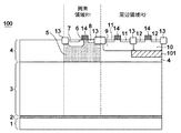
図1〜5を参照しながら第1実施形態を説明する。図1は、本実施形態の固体撮像装置100の構造を説明する模式図である。固体撮像装置100は、画素が配列された画素領域R1と、各画素との間で信号の授受を行うためのユニットが配された周辺領域R2とを有する。ここでは説明の容易化のため、画素領域R1に1画素を示している。周辺領域R2のユニットは、例えば、各画素を駆動するための駆動部、各画素から読み出された信号を処理するための信号処理部、各画素から読み出された信号を出力するための出力部のうちの1つまたは複数を含む。
図6を参照しながら第2実施形態を説明する。本実施形態は、P型半導体領域10の下にN型半導体領域101が設けられている点で第1実施形態と異なる。N型半導体領域101は、N型半導体領域4の不純物濃度よりも高い。第1実施形態(図1)の構造によると、周辺領域R2において、P型半導体領域10とN型半導体領域4とP型半導体領域3とによるPNPの寄生バイポーラトランジスタが形成されている。一方、本実施形態の構造によると、高不純物濃度領域であるN型半導体領域101により、該寄生バイポーラトランジスタがオンすることが防止される。よって、本実施形態によると、第1実施形態と同様の効果が得られる他、固体撮像装置100の動作の安定化にさらに有利である。
また、以上の実施形態は、カメラ等に代表される撮像システムに含まれる固体撮像装置について述べた。撮像システムの概念には、撮影を主目的とする装置のみならず、撮影機能を補助的に備える装置(例えば、パーソナルコンピュータ、携帯端末)も含まれる。撮像システムは、上記の実施形態として例示された本発明に係る固体撮像装置と、この固体撮像装置から出力される信号を処理する処理部とを含みうる。この処理部は、例えば、A/D変換器、および、このA/D変換器から出力されるデジタルデータを処理するプロセッサを含みうる。
Claims (23)
- 基板の上に配されたエピタキシャル層であって、前記基板からの位置が遠くなるのに従って不純物濃度が低くなる不純物濃度分布を持つ第1導電型の第1半導体領域と、
前記第1半導体領域の上に設けられた前記第1導電型の第2半導体領域と、
前記第2半導体領域に、前記第2半導体領域との間でPN接合を形成するように設けられた第2導電型の第3半導体領域と、を備え、
前記基板、前記第1半導体領域、前記第2半導体領域および前記第3半導体領域を含む構造体の深さ方向において、前記第2半導体領域が、前記第3半導体領域の側から順に、第1領域、第2領域、第3領域を有し、
前記第1領域および前記第3領域における前記第1導電型の不純物濃度のピークが前記第2領域における前記第1導電型の不純物濃度のピークより高い、
ことを特徴とする固体撮像装置。 - 前記第1領域における前記第1導電型の不純物濃度のピークが前記第3領域における前記第1導電型の不純物濃度のピークより高い、
ことを特徴とする請求項1に記載の固体撮像装置。 - 前記第1半導体領域の上に、前記第1半導体領域に接しつつ前記第2半導体領域と隣接するように設けられた前記第2導電型の第4半導体領域を更に備える、
ことを特徴とする請求項1又は請求項2に記載の固体撮像装置。 - 前記第4半導体領域はエピタキシャル層である、
ことを特徴とする請求項3に記載の固体撮像装置。 - 各々が光電変換部を含む複数の画素と、該複数の画素との間で信号の授受を行うユニットと、を備えており、
前記ユニットは、前記第4半導体領域に設けられている、
ことを特徴とする請求項3又は4に記載の固体撮像装置。 - 前記ユニットは、MOSトランジスタを有しており、
前記第4半導体領域には、前記第1導電型のウェルが設けられ、
前記MOSトランジスタの前記第2導電型のソース領域及び前記第2導電型のドレイン領域は前記ウェルに設けられ、
前記ウェルと前記第4半導体領域との間には、前記第4半導体領域よりも不純物濃度が高い前記第2導電型の第5半導体領域が設けられている、
ことを特徴とする請求項5に記載の固体撮像装置。 - 前記第4半導体領域には、前記第2導電型の第2のウェルが設けられ、
前記第5半導体領域がある深さにおいて、前記第2のウェルの下の不純物濃度は、前記第5半導体領域の不純物濃度より低い、
ことを特徴とする請求項6に記載の固体撮像装置。 - 前記第4半導体領域の厚さは、1μm以上かつ10μm以下の範囲内である、
ことを特徴とする請求項3乃至7のいずれか1項に記載の固体撮像装置。 - 前記第4半導体領域における前記第2導電型の不純物濃度が1×10¹⁴〜1×1015cm−3の範囲内である、
ことを特徴とする請求項3乃至8のいずれか1項に記載の固体撮像装置。 - 前記第1半導体領域の厚さは、5μm以上かつ500μm以下の範囲内である、
ことを特徴とする請求項1乃至9のいずれか1項に記載の固体撮像装置。 - 前記第2半導体領域の厚さは、1μm以上かつ10μm以下の範囲内である、
ことを特徴とする請求項1乃至10のいずれか1項に記載の固体撮像装置。 - 前記基板と前記第1半導体領域との間に設けられた前記第1導電型の第6半導体領域をさらに備え、前記第6半導体領域は、前記第1導電型の不純物濃度が前記第1半導体領域よりも高い、
ことを特徴とする請求項1乃至11のいずれか1項に記載の固体撮像装置。 - 前記第3領域の不純物濃度ピークにおける不純物濃度と、前記第1半導体領域の不純物濃度とが、第1型半導体領域と第2半導体領域5との境界領域にポテンシャル障壁が生じないように設定されている、
ことを特徴とする請求項1乃至12のいずれか1項に記載の固体撮像装置。 - 請求項1乃至13のいずれか1項に記載の固体撮像装置と、
前記固体撮像装置によって得られた近赤外光の画像と可視光の画像とを重ね合わせて出力する表示部と、を備える、
ことを特徴とする撮像システム。 - 基板の上に、エピタキシャル成長法により、第1導電型の第1半導体領域を、前記第1導電型の不純物濃度が前記基板からの位置が遠くなるのに従って低くなるように形成する工程と、
前記第1半導体領域にイオン注入を行って、前記第1導電型の第2半導体領域を形成する工程と、
前記第2半導体領域に、前記第2半導体領域との間でPN接合を形成するように、光電変換部の電荷蓄積領域となる第2導電型の第3半導体領域を形成する工程と、を有し、
前記第2半導体領域を形成する工程では、
前記基板、前記第1半導体領域、前記第2半導体領域および前記第3半導体領域を含む構造体の深さ方向において、前記第2半導体領域が、前記第3半導体領域の側から順に、第1領域、第2領域、第3領域を有し、
前記第1領域および前記第3領域における前記第1導電型の不純物濃度のピークが前記第2領域における前記第1導電型の不純物濃度のピークより高くなるように、
前記第2半導体領域を形成する、
ことを特徴とする固体撮像装置の製造方法。 - 基板の上に、エピタキシャル成長法により、第1導電型の第1半導体領域を、前記第1導電型の不純物濃度が前記基板からの位置が遠くなるのに従って低くなるように形成する工程と、
前記第1半導体領域の上に、エピタキシャル成長法により、第2導電型の第4半導体領域を形成する工程と、
前記第4半導体領域の一部にイオン注入を行って、前記第1導電型の第2半導体領域を形成する工程と、
前記第2半導体領域に、前記第2半導体領域との間でPN接合を形成するように、光電変換部の電荷蓄積領域となる前記第2導電型の第3半導体領域を形成する工程と、を有し、
前記第2半導体領域を形成する工程では、
前記基板、前記第1半導体領域、前記第2半導体領域および前記第3半導体領域を含む構造体の深さ方向において、前記第2半導体領域が、前記第3半導体領域の側から順に、第1領域、第2領域、第3領域を有し、
前記第1領域および前記第3領域における前記第1導電型の不純物濃度のピークが前記第2領域における前記第1導電型の不純物濃度のピークより高くなるように、
前記第2半導体領域を形成する、
ことを特徴とする固体撮像装置の製造方法。 - 前記第2半導体領域を形成する工程では、前記第1領域における前記第1導電型の不純物濃度のピークが前記第3領域における前記第1導電型の不純物濃度のピークより高くなるように、前記第2半導体領域を形成する、
ことを特徴とする請求項15又は16に記載の固体撮像装置の製造方法。 - 前記第1領域を形成するためのイオン注入と、前記第2領域を形成するためのイオン注入とが互いに異なる条件でなされる
ことを特徴とする請求項15乃至17のいずれか1項に記載の固体撮像装置の製造方法。 - 前記第4半導体領域の前記一部とは別の部分に、前記光電変換部からの信号を処理するユニットを形成する工程を含む、
ことを特徴とする請求項16に記載の固体撮像装置の製造方法。 - 前記ユニットは、MOSトランジスタを有しており、
前記第4半導体領域の前記別の部分に、前記第1導電型のウェルを形成する工程と、
前記MOSトランジスタの前記第2導電型のソース領域および前記第2導電型のドレイン領域を前記ウェルに形成する工程と、
前記ウェルと前記第1半導体領域との間の領域の不純物濃度を、前記第4半導体領域の不純物濃度よりも高くする工程と、を有する、
ことを特徴とする請求項19に記載の固体撮像装置の製造方法。 - 前記第1半導体領域を形成する工程では、前記第1半導体領域の厚さが5μm以上かつ500μm以下の範囲内になるように前記第1半導体領域を形成する、
ことを特徴とする請求項15乃至20のいずれか1項に記載の固体撮像装置の製造方法。 - 前記第2半導体領域を形成する工程では、前記第2半導体領域の厚さが1μm以上かつ10μm以下の範囲内になるように前記第2半導体領域を形成する、
ことを特徴とする請求項15乃至21のいずれか1項に記載の固体撮像装置の製造方法。 - 前記第1半導体領域を形成する工程の前に、前記基板に対して前記第1導電型の不純物を注入して前記第1導電型の第6半導体領域を形成する工程をさらに有し、
前記第6半導体領域は、前記第1導電型の不純物濃度が前記第1半導体領域よりも高い、
ことを特徴とする請求項15乃至22のいずれか1項に記載の固体撮像装置の製造方法。
Priority Applications (7)
| Application Number | Priority Date | Filing Date | Title |
|---|---|---|---|
| JP2013210588A JP6355311B2 (ja) | 2013-10-07 | 2013-10-07 | 固体撮像装置、その製造方法及び撮像システム |
| EP14184612.1A EP2866260B1 (en) | 2013-10-07 | 2014-09-12 | Solid-state imaging apparatus, method for manufacturing the same, and imaging system |
| US14/489,812 US9761618B2 (en) | 2013-10-07 | 2014-09-18 | Solid-state imaging apparatus, method for manufacturing the same, and imaging system |
| CN201410499673.6A CN104517983B (zh) | 2013-10-07 | 2014-09-26 | 固态成像装置、其制造方法和成像系统 |
| RU2014139258/28A RU2589519C2 (ru) | 2013-10-07 | 2014-09-29 | Твердотельное устройство формирования изображения, способ изготовления этого устройства и система формирования изображения |
| US15/637,155 US9947702B2 (en) | 2013-10-07 | 2017-06-29 | Solid-state imaging apparatus, method for manufacturing the same, and imaging system |
| US15/908,997 US10217780B2 (en) | 2013-10-07 | 2018-03-01 | Solid-state imaging apparatus, method for manufacturing the same, and imaging system |
Applications Claiming Priority (1)
| Application Number | Priority Date | Filing Date | Title |
|---|---|---|---|
| JP2013210588A JP6355311B2 (ja) | 2013-10-07 | 2013-10-07 | 固体撮像装置、その製造方法及び撮像システム |
Related Child Applications (1)
| Application Number | Title | Priority Date | Filing Date |
|---|---|---|---|
| JP2018107831A Division JP2018139328A (ja) | 2018-06-05 | 2018-06-05 | 固体撮像装置および撮像システム |
Publications (3)
| Publication Number | Publication Date |
|---|---|
| JP2015076453A JP2015076453A (ja) | 2015-04-20 |
| JP2015076453A5 JP2015076453A5 (ja) | 2016-08-18 |
| JP6355311B2 true JP6355311B2 (ja) | 2018-07-11 |
Family
ID=51518700
Family Applications (1)
| Application Number | Title | Priority Date | Filing Date |
|---|---|---|---|
| JP2013210588A Active JP6355311B2 (ja) | 2013-10-07 | 2013-10-07 | 固体撮像装置、その製造方法及び撮像システム |
Country Status (5)
| Country | Link |
|---|---|
| US (3) | US9761618B2 (ja) |
| EP (1) | EP2866260B1 (ja) |
| JP (1) | JP6355311B2 (ja) |
| CN (1) | CN104517983B (ja) |
| RU (1) | RU2589519C2 (ja) |
Families Citing this family (11)
| Publication number | Priority date | Publication date | Assignee | Title |
|---|---|---|---|---|
| JP6355311B2 (ja) * | 2013-10-07 | 2018-07-11 | キヤノン株式会社 | 固体撮像装置、その製造方法及び撮像システム |
| JP6274567B2 (ja) | 2014-03-14 | 2018-02-07 | キヤノン株式会社 | 固体撮像装置及び撮像システム |
| JP6595750B2 (ja) | 2014-03-14 | 2019-10-23 | キヤノン株式会社 | 固体撮像装置及び撮像システム |
| JP6579774B2 (ja) * | 2015-03-30 | 2019-09-25 | キヤノン株式会社 | 固体撮像装置およびカメラ |
| US9900539B2 (en) | 2015-09-10 | 2018-02-20 | Canon Kabushiki Kaisha | Solid-state image pickup element, and image pickup system |
| JP6541523B2 (ja) | 2015-09-11 | 2019-07-10 | キヤノン株式会社 | 撮像装置、撮像システム、および、撮像装置の制御方法 |
| JP6570384B2 (ja) | 2015-09-11 | 2019-09-04 | キヤノン株式会社 | 撮像装置及び撮像システム |
| US10205894B2 (en) | 2015-09-11 | 2019-02-12 | Canon Kabushiki Kaisha | Imaging device and imaging system |
| JP6674219B2 (ja) | 2015-10-01 | 2020-04-01 | キヤノン株式会社 | 固体撮像装置及び撮像システム |
| JP6862129B2 (ja) * | 2016-08-29 | 2021-04-21 | キヤノン株式会社 | 光電変換装置および撮像システム |
| JP7121468B2 (ja) * | 2017-02-24 | 2022-08-18 | ブリルニクス シンガポール プライベート リミテッド | 固体撮像装置、固体撮像装置の製造方法、および電子機器 |
Family Cites Families (41)
| Publication number | Priority date | Publication date | Assignee | Title |
|---|---|---|---|---|
| JPS63142848A (ja) * | 1986-12-05 | 1988-06-15 | Matsushita Electric Ind Co Ltd | 半導体集積回路装置 |
| JPS63174358A (ja) * | 1987-01-14 | 1988-07-18 | Hitachi Ltd | 固体撮像素子 |
| JPH0191453A (ja) * | 1987-10-02 | 1989-04-11 | Fuji Photo Film Co Ltd | 固体撮像装置 |
| JP2508218B2 (ja) * | 1988-09-27 | 1996-06-19 | 日本電気株式会社 | 相補型mis集積回路 |
| JP3381281B2 (ja) * | 1992-10-31 | 2003-02-24 | ソニー株式会社 | 半導体装置 |
| JPH07273364A (ja) | 1994-04-01 | 1995-10-20 | Matsushita Electron Corp | 固体撮像装置およびその製造方法 |
| JP2798006B2 (ja) | 1995-05-19 | 1998-09-17 | 日本電気株式会社 | 赤外線固体撮像素子とその製造方法 |
| JPH1126741A (ja) * | 1997-07-04 | 1999-01-29 | Toshiba Corp | 固体撮像装置 |
| JPH11251567A (ja) * | 1998-03-05 | 1999-09-17 | Canon Inc | 光電変換装置 |
| JP4109743B2 (ja) * | 1998-03-19 | 2008-07-02 | 株式会社東芝 | 固体撮像装置 |
| US6310366B1 (en) * | 1999-06-16 | 2001-10-30 | Micron Technology, Inc. | Retrograde well structure for a CMOS imager |
| JP2002043557A (ja) * | 2000-07-21 | 2002-02-08 | Mitsubishi Electric Corp | 固体撮像素子を有する半導体装置およびその製造方法 |
| JP4270742B2 (ja) | 2000-11-30 | 2009-06-03 | Necエレクトロニクス株式会社 | 固体撮像装置 |
| JP4123415B2 (ja) | 2002-05-20 | 2008-07-23 | ソニー株式会社 | 固体撮像装置 |
| JP4510414B2 (ja) * | 2003-09-12 | 2010-07-21 | キヤノン株式会社 | 光電変換装置 |
| CN101369594B (zh) | 2003-12-12 | 2012-06-27 | 佳能株式会社 | 光电变换装置及其制造方法和摄像系统 |
| US7323731B2 (en) * | 2003-12-12 | 2008-01-29 | Canon Kabushiki Kaisha | Photoelectric conversion device, method of manufacturing photoelectric conversion device, and image pickup system |
| JP4174468B2 (ja) * | 2003-12-12 | 2008-10-29 | キヤノン株式会社 | 光電変換装置及び撮像システム |
| JP4612818B2 (ja) * | 2004-08-31 | 2011-01-12 | キヤノン株式会社 | 固体撮像素子、固体撮像装置及び撮像システム |
| JP5224633B2 (ja) | 2004-03-30 | 2013-07-03 | キヤノン株式会社 | 半導体装置の製造方法 |
| JP4984376B2 (ja) * | 2004-04-15 | 2012-07-25 | ソニー株式会社 | 固体撮像装置 |
| JP4211696B2 (ja) * | 2004-06-30 | 2009-01-21 | ソニー株式会社 | 固体撮像装置の製造方法 |
| JP2006197393A (ja) | 2005-01-14 | 2006-07-27 | Canon Inc | 固体撮像装置、カメラ、及び固体撮像装置の駆動方法 |
| US8049293B2 (en) * | 2005-03-07 | 2011-11-01 | Sony Corporation | Solid-state image pickup device, electronic apparatus using such solid-state image pickup device and method of manufacturing solid-state image pickup device |
| JP2008034836A (ja) * | 2006-07-03 | 2008-02-14 | Univ Kinki | 固体撮像素子 |
| JP5328207B2 (ja) * | 2008-04-01 | 2013-10-30 | キヤノン株式会社 | 固体撮像装置 |
| JP2010056402A (ja) * | 2008-08-29 | 2010-03-11 | Panasonic Corp | 固体撮像素子 |
| JP2009088545A (ja) | 2008-11-28 | 2009-04-23 | Nec Electronics Corp | 固体撮像装置 |
| JP2010177594A (ja) * | 2009-01-30 | 2010-08-12 | Yamaha Corp | 固体撮像装置 |
| JP2010206181A (ja) | 2009-02-06 | 2010-09-16 | Canon Inc | 光電変換装置及び撮像システム |
| JP5522980B2 (ja) * | 2009-06-18 | 2014-06-18 | キヤノン株式会社 | 固体撮像装置、固体撮像装置を用いた撮像システム、および固体撮像装置の製造方法 |
| JP5306123B2 (ja) * | 2009-09-11 | 2013-10-02 | 株式会社東芝 | 裏面照射型固体撮像装置 |
| JP5546222B2 (ja) | 2009-12-04 | 2014-07-09 | キヤノン株式会社 | 固体撮像装置及び製造方法 |
| JP2011205040A (ja) | 2010-03-26 | 2011-10-13 | Brainvision Inc | 半導体基板および光電変換素子ならびにそれらの製造方法 |
| JP5726005B2 (ja) * | 2010-08-02 | 2015-05-27 | アイメックImec | Cmos撮像装置アレイの製造方法 |
| JP5677238B2 (ja) * | 2011-08-29 | 2015-02-25 | 株式会社日立製作所 | 固体撮像装置 |
| JP5864990B2 (ja) | 2011-10-03 | 2016-02-17 | キヤノン株式会社 | 固体撮像装置およびカメラ |
| JP5967915B2 (ja) | 2011-12-09 | 2016-08-10 | キヤノン株式会社 | 固体撮像装置の駆動方法 |
| JP6083930B2 (ja) * | 2012-01-18 | 2017-02-22 | キヤノン株式会社 | 光電変換装置および撮像システム、光電変換装置の製造方法 |
| JP5968146B2 (ja) | 2012-07-31 | 2016-08-10 | キヤノン株式会社 | 固体撮像装置およびカメラ |
| JP6355311B2 (ja) * | 2013-10-07 | 2018-07-11 | キヤノン株式会社 | 固体撮像装置、その製造方法及び撮像システム |
-
2013
- 2013-10-07 JP JP2013210588A patent/JP6355311B2/ja active Active
-
2014
- 2014-09-12 EP EP14184612.1A patent/EP2866260B1/en active Active
- 2014-09-18 US US14/489,812 patent/US9761618B2/en not_active Expired - Fee Related
- 2014-09-26 CN CN201410499673.6A patent/CN104517983B/zh active Active
- 2014-09-29 RU RU2014139258/28A patent/RU2589519C2/ru active
-
2017
- 2017-06-29 US US15/637,155 patent/US9947702B2/en active Active
-
2018
- 2018-03-01 US US15/908,997 patent/US10217780B2/en active Active
Also Published As
| Publication number | Publication date |
|---|---|
| JP2015076453A (ja) | 2015-04-20 |
| EP2866260A3 (en) | 2015-08-26 |
| US20160027825A1 (en) | 2016-01-28 |
| CN104517983A (zh) | 2015-04-15 |
| US9761618B2 (en) | 2017-09-12 |
| US10217780B2 (en) | 2019-02-26 |
| US20180261637A1 (en) | 2018-09-13 |
| CN104517983B (zh) | 2018-01-05 |
| RU2014139258A (ru) | 2016-04-20 |
| RU2589519C2 (ru) | 2016-07-10 |
| US9947702B2 (en) | 2018-04-17 |
| EP2866260B1 (en) | 2019-02-06 |
| EP2866260A2 (en) | 2015-04-29 |
| US20170317121A1 (en) | 2017-11-02 |
Similar Documents
| Publication | Publication Date | Title |
|---|---|---|
| JP6355311B2 (ja) | 固体撮像装置、その製造方法及び撮像システム | |
| TWI225304B (en) | Solid-state image sensing device and camera system using the same | |
| KR102404288B1 (ko) | 고체 촬상 소자 및 고체 촬상 소자의 제조 방법, 및 전자 기기 | |
| JP6406585B2 (ja) | 撮像装置 | |
| US9711558B2 (en) | Imaging device with photoelectric converter | |
| JP5971565B2 (ja) | 固体撮像装置 | |
| US10325955B2 (en) | CMOS image sensor with backside biased substrate | |
| JP2009541992A (ja) | 低クロストークpmosピクセル構造 | |
| TW201222801A (en) | Photodetector isolation in image sensors | |
| TW201312740A (zh) | 固體攝像元件 | |
| JP2009510777A (ja) | 改善された収集のための光検出器及びn型層構造 | |
| US9287319B2 (en) | CMOS multi-pinned (MP) pixel | |
| TWI451564B (zh) | 具有二磊晶層之影像感測器及其製造方法 | |
| JP2009065155A (ja) | イメージセンサー | |
| CN101471361B (zh) | 图像传感器及其制造方法 | |
| US20140124839A1 (en) | Pixel architecture and method | |
| JP2009065156A (ja) | イメージセンサーの製造方法 | |
| JP2017220603A (ja) | 固体撮像素子および固体撮像素子の製造方法 | |
| CN109638025A (zh) | Cmos图像传感器及其制备方法 | |
| JP2018139328A (ja) | 固体撮像装置および撮像システム | |
| JP2009302448A (ja) | 固体撮像素子の製造方法 | |
| JP7199013B2 (ja) | 光検出器 | |
| KR101038886B1 (ko) | 이미지센서 및 그 제조방법 |
Legal Events
| Date | Code | Title | Description |
|---|---|---|---|
| A521 | Request for written amendment filed |
Free format text: JAPANESE INTERMEDIATE CODE: A523 Effective date: 20160629 |
|
| A621 | Written request for application examination |
Free format text: JAPANESE INTERMEDIATE CODE: A621 Effective date: 20160629 |
|
| A977 | Report on retrieval |
Free format text: JAPANESE INTERMEDIATE CODE: A971007 Effective date: 20170208 |
|
| A131 | Notification of reasons for refusal |
Free format text: JAPANESE INTERMEDIATE CODE: A131 Effective date: 20170313 |
|
| A521 | Request for written amendment filed |
Free format text: JAPANESE INTERMEDIATE CODE: A523 Effective date: 20170501 |
|
| A131 | Notification of reasons for refusal |
Free format text: JAPANESE INTERMEDIATE CODE: A131 Effective date: 20171030 |
|
| A521 | Request for written amendment filed |
Free format text: JAPANESE INTERMEDIATE CODE: A523 Effective date: 20171208 |
|
| TRDD | Decision of grant or rejection written | ||
| A01 | Written decision to grant a patent or to grant a registration (utility model) |
Free format text: JAPANESE INTERMEDIATE CODE: A01 Effective date: 20180514 |
|
| A61 | First payment of annual fees (during grant procedure) |
Free format text: JAPANESE INTERMEDIATE CODE: A61 Effective date: 20180612 |
|
| R151 | Written notification of patent or utility model registration |
Ref document number: 6355311 Country of ref document: JP Free format text: JAPANESE INTERMEDIATE CODE: R151 |