JP4510414B2 - 光電変換装置 - Google Patents
光電変換装置 Download PDFInfo
- Publication number
- JP4510414B2 JP4510414B2 JP2003321533A JP2003321533A JP4510414B2 JP 4510414 B2 JP4510414 B2 JP 4510414B2 JP 2003321533 A JP2003321533 A JP 2003321533A JP 2003321533 A JP2003321533 A JP 2003321533A JP 4510414 B2 JP4510414 B2 JP 4510414B2
- Authority
- JP
- Japan
- Prior art keywords
- conductivity type
- well
- type
- photoelectric conversion
- buried layer
- Prior art date
- Legal status (The legal status is an assumption and is not a legal conclusion. Google has not performed a legal analysis and makes no representation as to the accuracy of the status listed.)
- Expired - Fee Related
Links
- 238000006243 chemical reaction Methods 0.000 title claims description 29
- 239000000758 substrate Substances 0.000 claims description 33
- 239000004065 semiconductor Substances 0.000 claims description 19
- 238000009792 diffusion process Methods 0.000 claims description 8
- 230000004888 barrier function Effects 0.000 claims description 5
- 239000012535 impurity Substances 0.000 claims description 5
- 238000000034 method Methods 0.000 description 20
- 238000002955 isolation Methods 0.000 description 12
- 230000002093 peripheral effect Effects 0.000 description 10
- 238000010586 diagram Methods 0.000 description 8
- 238000005468 ion implantation Methods 0.000 description 8
- 230000001133 acceleration Effects 0.000 description 7
- 150000002500 ions Chemical class 0.000 description 7
- ZOXJGFHDIHLPTG-UHFFFAOYSA-N Boron Chemical compound [B] ZOXJGFHDIHLPTG-UHFFFAOYSA-N 0.000 description 6
- 229910052796 boron Inorganic materials 0.000 description 6
- OAICVXFJPJFONN-UHFFFAOYSA-N Phosphorus Chemical compound [P] OAICVXFJPJFONN-UHFFFAOYSA-N 0.000 description 5
- 229910052698 phosphorus Inorganic materials 0.000 description 5
- 239000011574 phosphorus Substances 0.000 description 5
- 238000004519 manufacturing process Methods 0.000 description 3
- 238000000206 photolithography Methods 0.000 description 3
- 230000035945 sensitivity Effects 0.000 description 3
- 230000003595 spectral effect Effects 0.000 description 3
- 238000003860 storage Methods 0.000 description 3
- -1 E12 ions Chemical class 0.000 description 2
- KRHYYFGTRYWZRS-UHFFFAOYSA-N Fluorane Chemical compound F KRHYYFGTRYWZRS-UHFFFAOYSA-N 0.000 description 2
- 229910004298 SiO 2 Inorganic materials 0.000 description 2
- 230000015572 biosynthetic process Effects 0.000 description 2
- 239000000463 material Substances 0.000 description 2
- 238000000059 patterning Methods 0.000 description 2
- 238000005229 chemical vapour deposition Methods 0.000 description 1
- SLLGVCUQYRMELA-UHFFFAOYSA-N chlorosilicon Chemical compound Cl[Si] SLLGVCUQYRMELA-UHFFFAOYSA-N 0.000 description 1
- 238000007796 conventional method Methods 0.000 description 1
- 238000009826 distribution Methods 0.000 description 1
- 238000010438 heat treatment Methods 0.000 description 1
- 238000002513 implantation Methods 0.000 description 1
- 238000001459 lithography Methods 0.000 description 1
- 239000012299 nitrogen atmosphere Substances 0.000 description 1
- 230000003647 oxidation Effects 0.000 description 1
- 238000007254 oxidation reaction Methods 0.000 description 1
- 230000003071 parasitic effect Effects 0.000 description 1
- 238000002360 preparation method Methods 0.000 description 1
- 238000000926 separation method Methods 0.000 description 1
Images


Classifications
-
- H—ELECTRICITY
- H10—SEMICONDUCTOR DEVICES; ELECTRIC SOLID-STATE DEVICES NOT OTHERWISE PROVIDED FOR
- H10F—INORGANIC SEMICONDUCTOR DEVICES SENSITIVE TO INFRARED RADIATION, LIGHT, ELECTROMAGNETIC RADIATION OF SHORTER WAVELENGTH OR CORPUSCULAR RADIATION
- H10F39/00—Integrated devices, or assemblies of multiple devices, comprising at least one element covered by group H10F30/00, e.g. radiation detectors comprising photodiode arrays
- H10F39/011—Manufacture or treatment of image sensors covered by group H10F39/12
- H10F39/026—Wafer-level processing
-
- H—ELECTRICITY
- H10—SEMICONDUCTOR DEVICES; ELECTRIC SOLID-STATE DEVICES NOT OTHERWISE PROVIDED FOR
- H10F—INORGANIC SEMICONDUCTOR DEVICES SENSITIVE TO INFRARED RADIATION, LIGHT, ELECTROMAGNETIC RADIATION OF SHORTER WAVELENGTH OR CORPUSCULAR RADIATION
- H10F39/00—Integrated devices, or assemblies of multiple devices, comprising at least one element covered by group H10F30/00, e.g. radiation detectors comprising photodiode arrays
- H10F39/80—Constructional details of image sensors
- H10F39/807—Pixel isolation structures
Landscapes
- Solid State Image Pick-Up Elements (AREA)
- Light Receiving Elements (AREA)
Description
次に、SiHCl3を用いたCVD法にて、Si基体201表面に、Siのエピタキシャル層203を成長させる。本実施例では、センサの分光感度を鑑み、厚さ4μm、比抵抗10Ω・cmでN型の物を成長させた。(図2−(b)参照)
本実施例とは別に、基体201に、直接エピタキシャル層203を堆積させ、しかる後に、高エネルギーイオン注入法等の手法を用いて、埋め込み層202を形成しても、図2−(b)のような構造体を形成することは、可能である。
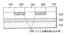
次に、エピタキシャル層203のN型のウエル207を形成しなかった領域の一部に、フォトリソグラフィ法によって、P型のウエル206の領域をレジスト209にて規定する。ここで、まず、P型のウエルを形成するための、ホウ素を、以下の3段階にて打ち込む。最も深い領域には、3E12ions/cm2のドーズ量及び250KeVの加速電圧で、中間領域には、2.5E12ions/cm2のドーズ量及び125KeVの加速電圧で、最表面には、3.8E12ions/cm2のドーズ量及び35KeVの加速電圧で、ホウ素を打ち込む。
この後、レジスト209を除去すれば、図1のような、構造体を作ることができる。
102,202,302,402 半導体基体全面に延在する埋め込み層
103,203,303,403 エピタキシャル層
304,404 フォトダイオードの障壁拡散層
305,405 フォトダイオードの電荷蓄積拡散層
106,206,306 半導体基体と反対導電型のウエル
107,207,307 半導体基体と同一導電型のウエル
108,208,308 半導体基体と同一導電型のウエル分離用埋め込み層
309 MOSFETのゲート電極
310 ソース−ドレイン領域
Claims (6)
- 第1導電型の半導体基体と、
前記第1導電型の半導体基体上に配され、光電変換素子が配された第1の領域と駆動回路が配された第2の領域とを有する第1導電型のエピタキシャル層と、
前記第1導電型の半導体基体と前記第1導電型のエピタキシャル層との間に配され、前記第1導電型の半導体基体の全面に延在する第2導電型の第1の埋め込み層と、
前記第1導電型のエピタキシャル層内の前記第2の領域に配され、第1導電型のMOSFETのソース及びドレインを有する第2導電型の第1のウエルと、を有する光電変換装置において、
前記第2導電型の第1のウエルと前記第1導電型のエピタキシャル層との間に配され、前記第2導電型の第1のウエルの下部全面に接して延在し、前記第1導電型のエピタキシャル層よりも高い不純物濃度を有する第1導電型の第2の埋め込み層を有することを特徴とする光電変換装置。 - 前記第2導電型の第1のウエルが間隔を空けて複数配されており、
複数の前記第2導電型の第1のウエルのそれぞれの下部に前記第1導電型の第2の埋め込み層が配されていることを特徴とする請求項1に記載の光電変換装置。 - 複数の前記第2導電型の第1のウエルの間に、第1導電型のウエルが配され、該第1導電型のウエル内に第2導電型のMOSFETが配されていることを特徴とする請求項2に記載の光電変換装置。
- 前記第1導電型の第2の埋め込み層は、前記第2導電型の第1のウエルに対してセルフアラインで形成されていることを特徴とする請求項1乃至3のいずれか1項に記載の光電変換装置。
- 前記第1導電型のエピタキシャル層内の前記第1の領域に配され、前記光電変換素子が配された第2導電型の第2のウエルと、
前記第2導電型の第2のウエルと前記第1導電型のエピタキシャル層との間に配され、前記第2導電型の第2のウエルの下部全面に接して延在し、前記第1導電型のエピタキシャル層よりも高い不純物濃度を有する第1導電型の第3の埋め込み層と、
前記第2導電型の第2のウエルに配され、前記第1導電型の第3の埋め込み層と接する前記光電変換素子の障壁拡散層とを有することを特徴とする請求項1乃至4のいずれか1項に記載の光電変換装置。 - 前記第1導電型の第3の埋め込み層は、前記第2導電型の第2のウエルに対してセルフアラインで形成されていることを特徴とする請求項5に記載の光電変換装置。
Priority Applications (2)
| Application Number | Priority Date | Filing Date | Title |
|---|---|---|---|
| JP2003321533A JP4510414B2 (ja) | 2003-09-12 | 2003-09-12 | 光電変換装置 |
| US10/937,382 US7247899B2 (en) | 2003-09-12 | 2004-09-10 | Semiconductor device, photoelectric conversion device and method of manufacturing same |
Applications Claiming Priority (1)
| Application Number | Priority Date | Filing Date | Title |
|---|---|---|---|
| JP2003321533A JP4510414B2 (ja) | 2003-09-12 | 2003-09-12 | 光電変換装置 |
Publications (3)
| Publication Number | Publication Date |
|---|---|
| JP2005093525A JP2005093525A (ja) | 2005-04-07 |
| JP2005093525A5 JP2005093525A5 (ja) | 2006-10-26 |
| JP4510414B2 true JP4510414B2 (ja) | 2010-07-21 |
Family
ID=34269957
Family Applications (1)
| Application Number | Title | Priority Date | Filing Date |
|---|---|---|---|
| JP2003321533A Expired - Fee Related JP4510414B2 (ja) | 2003-09-12 | 2003-09-12 | 光電変換装置 |
Country Status (2)
| Country | Link |
|---|---|
| US (1) | US7247899B2 (ja) |
| JP (1) | JP4510414B2 (ja) |
Families Citing this family (9)
| Publication number | Priority date | Publication date | Assignee | Title |
|---|---|---|---|---|
| US8513753B1 (en) * | 2004-09-14 | 2013-08-20 | Cypress Semiconductor Corporation | Photodiode having a buried well region |
| JP4667030B2 (ja) * | 2004-12-10 | 2011-04-06 | キヤノン株式会社 | 固体撮像装置用の半導体基板とその製造方法 |
| JP5272281B2 (ja) * | 2005-09-22 | 2013-08-28 | ソニー株式会社 | 固体撮像装置およびその製造方法、並びにカメラ |
| JP4679340B2 (ja) * | 2005-11-11 | 2011-04-27 | 株式会社東芝 | 固体撮像装置 |
| KR101565750B1 (ko) | 2009-04-10 | 2015-11-05 | 삼성전자 주식회사 | 고감도 이미지 센서 |
| CN102479793B (zh) * | 2010-11-29 | 2014-01-15 | 格科微电子(上海)有限公司 | Cmos图像传感器及其制造方法 |
| WO2012176454A1 (ja) * | 2011-06-22 | 2012-12-27 | パナソニック株式会社 | 固体撮像装置 |
| JP6355311B2 (ja) | 2013-10-07 | 2018-07-11 | キヤノン株式会社 | 固体撮像装置、その製造方法及び撮像システム |
| JP2018139328A (ja) * | 2018-06-05 | 2018-09-06 | キヤノン株式会社 | 固体撮像装置および撮像システム |
Citations (10)
| Publication number | Priority date | Publication date | Assignee | Title |
|---|---|---|---|---|
| JPH03214666A (ja) * | 1990-01-19 | 1991-09-19 | Toshiba Corp | 電荷転送デバイスを含む半導体装置およびその製造方法 |
| JPH06205158A (ja) * | 1993-01-01 | 1994-07-22 | Canon Inc | 固体撮像装置 |
| JPH07254691A (ja) * | 1994-03-15 | 1995-10-03 | Olympus Optical Co Ltd | 固体撮像装置の製造方法 |
| JPH09246514A (ja) * | 1996-03-12 | 1997-09-19 | Sharp Corp | 増幅型固体撮像装置 |
| JP2000150848A (ja) * | 1998-11-09 | 2000-05-30 | Toshiba Corp | 固体撮像装置 |
| JP2000232214A (ja) * | 1999-02-12 | 2000-08-22 | Nikon Corp | 半導体集積回路および固体撮像素子 |
| JP2002203954A (ja) * | 2000-10-31 | 2002-07-19 | Sharp Corp | 回路内蔵受光素子 |
| JP2002231917A (ja) * | 2001-02-05 | 2002-08-16 | Hamamatsu Photonics Kk | 半導体光検出装置 |
| JP2002353146A (ja) * | 2001-05-23 | 2002-12-06 | Sony Corp | 半導体基板の製造装置およびそれによる半導体基板を使用する半導体装置の製造方法 |
| JP2003142672A (ja) * | 2001-10-31 | 2003-05-16 | Mitsubishi Electric Corp | 固体イメージセンサ及び固体イメージセンサの製造方法 |
Family Cites Families (13)
| Publication number | Priority date | Publication date | Assignee | Title |
|---|---|---|---|---|
| JPH07109860B2 (ja) * | 1990-01-19 | 1995-11-22 | 株式会社東芝 | 電荷転送デバイスを含む半導体装置およびその製造方法 |
| US5260228A (en) * | 1990-01-19 | 1993-11-09 | Kabushiki Kaisha Toshiba | Method of making a semiconductor device having a charge transfer device, MOSFETs, and bipolar transistors |
| JPH04176171A (ja) | 1990-11-07 | 1992-06-23 | Sharp Corp | 固体撮像装置 |
| US5248624A (en) * | 1991-08-23 | 1993-09-28 | Exar Corporation | Method of making isolated vertical pnp transistor in a complementary bicmos process with eeprom memory |
| JPH05226627A (ja) * | 1992-02-10 | 1993-09-03 | Sharp Corp | 半導体装置 |
| US5302534A (en) * | 1992-03-02 | 1994-04-12 | Motorola, Inc. | Forming a vertical PNP transistor |
| JP3252432B2 (ja) | 1992-03-19 | 2002-02-04 | 松下電器産業株式会社 | 半導体装置およびその製造方法 |
| US5534069A (en) * | 1992-07-23 | 1996-07-09 | Canon Kabushiki Kaisha | Method of treating active material |
| KR100192954B1 (ko) * | 1996-07-18 | 1999-06-15 | 김광호 | 수직형 전달게이트를 가지는 전하결합형 고체촬상소자 및 그 제조방법 |
| EP0883187A1 (en) * | 1997-06-04 | 1998-12-09 | Interuniversitair Micro-Elektronica Centrum Vzw | A detector for electromagnetic radiation, pixel structure with high sensitivity using such detector and method of manufacturing such detector |
| JP4419238B2 (ja) * | 1999-12-27 | 2010-02-24 | ソニー株式会社 | 固体撮像素子及びその製造方法 |
| KR100867574B1 (ko) * | 2002-05-09 | 2008-11-10 | 페어차일드코리아반도체 주식회사 | 고전압 디바이스 및 그 제조방법 |
| US7110028B1 (en) * | 2002-08-13 | 2006-09-19 | Foveon, Inc. | Electronic shutter using buried layers and active pixel sensor and array employing same |
-
2003
- 2003-09-12 JP JP2003321533A patent/JP4510414B2/ja not_active Expired - Fee Related
-
2004
- 2004-09-10 US US10/937,382 patent/US7247899B2/en not_active Expired - Fee Related
Patent Citations (10)
| Publication number | Priority date | Publication date | Assignee | Title |
|---|---|---|---|---|
| JPH03214666A (ja) * | 1990-01-19 | 1991-09-19 | Toshiba Corp | 電荷転送デバイスを含む半導体装置およびその製造方法 |
| JPH06205158A (ja) * | 1993-01-01 | 1994-07-22 | Canon Inc | 固体撮像装置 |
| JPH07254691A (ja) * | 1994-03-15 | 1995-10-03 | Olympus Optical Co Ltd | 固体撮像装置の製造方法 |
| JPH09246514A (ja) * | 1996-03-12 | 1997-09-19 | Sharp Corp | 増幅型固体撮像装置 |
| JP2000150848A (ja) * | 1998-11-09 | 2000-05-30 | Toshiba Corp | 固体撮像装置 |
| JP2000232214A (ja) * | 1999-02-12 | 2000-08-22 | Nikon Corp | 半導体集積回路および固体撮像素子 |
| JP2002203954A (ja) * | 2000-10-31 | 2002-07-19 | Sharp Corp | 回路内蔵受光素子 |
| JP2002231917A (ja) * | 2001-02-05 | 2002-08-16 | Hamamatsu Photonics Kk | 半導体光検出装置 |
| JP2002353146A (ja) * | 2001-05-23 | 2002-12-06 | Sony Corp | 半導体基板の製造装置およびそれによる半導体基板を使用する半導体装置の製造方法 |
| JP2003142672A (ja) * | 2001-10-31 | 2003-05-16 | Mitsubishi Electric Corp | 固体イメージセンサ及び固体イメージセンサの製造方法 |
Also Published As
| Publication number | Publication date |
|---|---|
| US7247899B2 (en) | 2007-07-24 |
| US20050056905A1 (en) | 2005-03-17 |
| JP2005093525A (ja) | 2005-04-07 |
Similar Documents
| Publication | Publication Date | Title |
|---|---|---|
| JP7279277B2 (ja) | 複数遮蔽トレンチゲートfet | |
| JPH09120995A (ja) | 半導体装置およびその製造方法 | |
| JPH07183393A (ja) | 半導体装置の製造方法 | |
| JP2004241613A (ja) | 半導体装置 | |
| JP4510414B2 (ja) | 光電変換装置 | |
| JP3954140B2 (ja) | 半導体装置及びその製造方法 | |
| JPH0824144B2 (ja) | 半導体装置の製造方法 | |
| JPH077773B2 (ja) | 半導体装置の製造方法 | |
| JPS59111359A (ja) | 半導体構造体の製造方法 | |
| JP2745228B2 (ja) | 半導体装置およびその製造方法 | |
| CN100490116C (zh) | 半导体器件及其制造方法 | |
| JP2014207324A (ja) | 半導体装置及びその製造方法 | |
| KR100582374B1 (ko) | 고전압 트랜지스터 및 그 제조 방법 | |
| JP2834058B2 (ja) | 半導体装置の製造方法 | |
| JPH08316335A (ja) | 半導体装置およびその製造方法 | |
| JP2949745B2 (ja) | 縦型mos電界効果トランジスタの製造方法 | |
| JP4166031B2 (ja) | Mos半導体装置およびその製造方法 | |
| JP4147829B2 (ja) | 固体撮像装置の製造方法 | |
| JP2005044948A (ja) | 半導体装置、および、その製造方法 | |
| JP2007053399A (ja) | 半導体装置 | |
| JPH10163338A (ja) | 半導体装置とその製造方法 | |
| JP2003303959A (ja) | 縦型mos半導体装置およびその製造方法 | |
| JP6668600B2 (ja) | 固体撮像素子及びその製造方法 | |
| JP4118196B2 (ja) | 半導体素子、その製造方法および半導体装置 | |
| JP2611450B2 (ja) | 半導体集積回路及びその製造方法 |
Legal Events
| Date | Code | Title | Description |
|---|---|---|---|
| A521 | Request for written amendment filed |
Free format text: JAPANESE INTERMEDIATE CODE: A523 Effective date: 20060911 |
|
| A621 | Written request for application examination |
Free format text: JAPANESE INTERMEDIATE CODE: A621 Effective date: 20060911 |
|
| RD04 | Notification of resignation of power of attorney |
Free format text: JAPANESE INTERMEDIATE CODE: A7424 Effective date: 20080207 |
|
| RD03 | Notification of appointment of power of attorney |
Free format text: JAPANESE INTERMEDIATE CODE: A7423 Effective date: 20090326 |
|
| RD05 | Notification of revocation of power of attorney |
Free format text: JAPANESE INTERMEDIATE CODE: A7425 Effective date: 20090427 |
|
| A977 | Report on retrieval |
Free format text: JAPANESE INTERMEDIATE CODE: A971007 Effective date: 20091109 |
|
| A131 | Notification of reasons for refusal |
Free format text: JAPANESE INTERMEDIATE CODE: A131 Effective date: 20091113 |
|
| A521 | Request for written amendment filed |
Free format text: JAPANESE INTERMEDIATE CODE: A523 Effective date: 20100112 |
|
| TRDD | Decision of grant or rejection written | ||
| A01 | Written decision to grant a patent or to grant a registration (utility model) |
Free format text: JAPANESE INTERMEDIATE CODE: A01 Effective date: 20100427 |
|
| A01 | Written decision to grant a patent or to grant a registration (utility model) |
Free format text: JAPANESE INTERMEDIATE CODE: A01 |
|
| A61 | First payment of annual fees (during grant procedure) |
Free format text: JAPANESE INTERMEDIATE CODE: A61 Effective date: 20100430 |
|
| FPAY | Renewal fee payment (event date is renewal date of database) |
Free format text: PAYMENT UNTIL: 20130514 Year of fee payment: 3 |
|
| R150 | Certificate of patent or registration of utility model |
Free format text: JAPANESE INTERMEDIATE CODE: R150 |
|
| FPAY | Renewal fee payment (event date is renewal date of database) |
Free format text: PAYMENT UNTIL: 20140514 Year of fee payment: 4 |
|
| LAPS | Cancellation because of no payment of annual fees |