JP4510414B2 - Photoelectric conversion device - Google Patents
Photoelectric conversion device Download PDFInfo
- Publication number
- JP4510414B2 JP4510414B2 JP2003321533A JP2003321533A JP4510414B2 JP 4510414 B2 JP4510414 B2 JP 4510414B2 JP 2003321533 A JP2003321533 A JP 2003321533A JP 2003321533 A JP2003321533 A JP 2003321533A JP 4510414 B2 JP4510414 B2 JP 4510414B2
- Authority
- JP
- Japan
- Prior art keywords
- conductivity type
- well
- type
- photoelectric conversion
- buried layer
- Prior art date
- Legal status (The legal status is an assumption and is not a legal conclusion. Google has not performed a legal analysis and makes no representation as to the accuracy of the status listed.)
- Expired - Fee Related
Links
- 238000006243 chemical reaction Methods 0.000 title claims description 29
- 239000000758 substrate Substances 0.000 claims description 33
- 239000004065 semiconductor Substances 0.000 claims description 19
- 238000009792 diffusion process Methods 0.000 claims description 8
- 230000004888 barrier function Effects 0.000 claims description 5
- 239000012535 impurity Substances 0.000 claims description 5
- 238000000034 method Methods 0.000 description 20
- 238000002955 isolation Methods 0.000 description 12
- 230000002093 peripheral effect Effects 0.000 description 10
- 238000010586 diagram Methods 0.000 description 8
- 238000005468 ion implantation Methods 0.000 description 8
- 230000001133 acceleration Effects 0.000 description 7
- 150000002500 ions Chemical class 0.000 description 7
- ZOXJGFHDIHLPTG-UHFFFAOYSA-N Boron Chemical compound [B] ZOXJGFHDIHLPTG-UHFFFAOYSA-N 0.000 description 6
- 229910052796 boron Inorganic materials 0.000 description 6
- OAICVXFJPJFONN-UHFFFAOYSA-N Phosphorus Chemical compound [P] OAICVXFJPJFONN-UHFFFAOYSA-N 0.000 description 5
- 229910052698 phosphorus Inorganic materials 0.000 description 5
- 239000011574 phosphorus Substances 0.000 description 5
- 238000004519 manufacturing process Methods 0.000 description 3
- 238000000206 photolithography Methods 0.000 description 3
- 230000035945 sensitivity Effects 0.000 description 3
- 230000003595 spectral effect Effects 0.000 description 3
- 238000003860 storage Methods 0.000 description 3
- -1 E12 ions Chemical class 0.000 description 2
- KRHYYFGTRYWZRS-UHFFFAOYSA-N Fluorane Chemical compound F KRHYYFGTRYWZRS-UHFFFAOYSA-N 0.000 description 2
- 229910004298 SiO 2 Inorganic materials 0.000 description 2
- 230000015572 biosynthetic process Effects 0.000 description 2
- 239000000463 material Substances 0.000 description 2
- 238000000059 patterning Methods 0.000 description 2
- 238000005229 chemical vapour deposition Methods 0.000 description 1
- SLLGVCUQYRMELA-UHFFFAOYSA-N chlorosilicon Chemical compound Cl[Si] SLLGVCUQYRMELA-UHFFFAOYSA-N 0.000 description 1
- 238000007796 conventional method Methods 0.000 description 1
- 238000009826 distribution Methods 0.000 description 1
- 238000010438 heat treatment Methods 0.000 description 1
- 238000002513 implantation Methods 0.000 description 1
- 238000001459 lithography Methods 0.000 description 1
- 239000012299 nitrogen atmosphere Substances 0.000 description 1
- 230000003647 oxidation Effects 0.000 description 1
- 238000007254 oxidation reaction Methods 0.000 description 1
- 230000003071 parasitic effect Effects 0.000 description 1
- 238000002360 preparation method Methods 0.000 description 1
- 238000000926 separation method Methods 0.000 description 1
Images


Classifications
-
- H—ELECTRICITY
- H01—ELECTRIC ELEMENTS
- H01L—SEMICONDUCTOR DEVICES NOT COVERED BY CLASS H10
- H01L27/00—Devices consisting of a plurality of semiconductor or other solid-state components formed in or on a common substrate
- H01L27/14—Devices consisting of a plurality of semiconductor or other solid-state components formed in or on a common substrate including semiconductor components sensitive to infrared radiation, light, electromagnetic radiation of shorter wavelength or corpuscular radiation and specially adapted either for the conversion of the energy of such radiation into electrical energy or for the control of electrical energy by such radiation
- H01L27/144—Devices controlled by radiation
- H01L27/146—Imager structures
- H01L27/14683—Processes or apparatus peculiar to the manufacture or treatment of these devices or parts thereof
- H01L27/14687—Wafer level processing
-
- H—ELECTRICITY
- H01—ELECTRIC ELEMENTS
- H01L—SEMICONDUCTOR DEVICES NOT COVERED BY CLASS H10
- H01L27/00—Devices consisting of a plurality of semiconductor or other solid-state components formed in or on a common substrate
- H01L27/14—Devices consisting of a plurality of semiconductor or other solid-state components formed in or on a common substrate including semiconductor components sensitive to infrared radiation, light, electromagnetic radiation of shorter wavelength or corpuscular radiation and specially adapted either for the conversion of the energy of such radiation into electrical energy or for the control of electrical energy by such radiation
- H01L27/144—Devices controlled by radiation
- H01L27/146—Imager structures
- H01L27/14601—Structural or functional details thereof
- H01L27/1463—Pixel isolation structures
-
- H—ELECTRICITY
- H01—ELECTRIC ELEMENTS
- H01L—SEMICONDUCTOR DEVICES NOT COVERED BY CLASS H10
- H01L27/00—Devices consisting of a plurality of semiconductor or other solid-state components formed in or on a common substrate
- H01L27/14—Devices consisting of a plurality of semiconductor or other solid-state components formed in or on a common substrate including semiconductor components sensitive to infrared radiation, light, electromagnetic radiation of shorter wavelength or corpuscular radiation and specially adapted either for the conversion of the energy of such radiation into electrical energy or for the control of electrical energy by such radiation
- H01L27/144—Devices controlled by radiation
- H01L27/146—Imager structures
- H01L27/14601—Structural or functional details thereof
- H01L27/14632—Wafer-level processed structures
Landscapes
- Physics & Mathematics (AREA)
- Engineering & Computer Science (AREA)
- Power Engineering (AREA)
- Electromagnetism (AREA)
- Condensed Matter Physics & Semiconductors (AREA)
- General Physics & Mathematics (AREA)
- Computer Hardware Design (AREA)
- Microelectronics & Electronic Packaging (AREA)
- Solid State Image Pick-Up Elements (AREA)
- Light Receiving Elements (AREA)
Description
本発明は、デジタルカメラ等の撮像素子として用いられる光電変換装置に関する。該光電変換装置は、フォトダイオードのアノードもしくはカソードの一部に埋め込み層を有した、センサ構造を持つCCDやCMOSセンサ等の半導体装置である。 The present invention relates to a photoelectric conversion device used as an image pickup device such as a digital camera. The photoelectric conversion device is a semiconductor device such as a CCD or CMOS sensor having a sensor structure having a buried layer in a part of an anode or a cathode of a photodiode.
従来の技術で、CCDやCMOSセンサのフォトダイオードに埋め込み層を有する光電変換装置がある。 As a conventional technique, there is a photoelectric conversion device having a buried layer in a photodiode of a CCD or a CMOS sensor.
図4は、従来の光電変換装置のフォトダイオード部分の断面構造を示す概念図である。 FIG. 4 is a conceptual diagram showing a cross-sectional structure of a photodiode portion of a conventional photoelectric conversion device.
401がSi等の半導体基体(一例としてN型)、402がフォトダイオード下部を規定する埋め込み層(一例としてP型)、403がエピタキシャル層(一例としてN型)、404がフォトダイオードの横方向の感光領域を規定する、障壁用の拡散層(一例としてP型)、405がフォトダイオードの電荷蓄積拡散層(一例としてN型)である。 401 is a semiconductor substrate such as Si (N-type as an example), 402 is a buried layer (P-type as an example) defining the lower part of the photodiode, 403 is an epitaxial layer (N-type as an example), and 404 is a lateral direction of the photodiode. A barrier diffusion layer (P-type as an example) that defines a photosensitive region, and 405 is a charge storage diffusion layer (N-type as an example) of a photodiode.
CCDとCMOSセンサで、フォトダイオード構造に関しては、同一の構成要件で考えることができる。この構造の場合は、埋め込み層402と、障壁拡散層404で、囲まれた領域が、個々のセンサの感光領域になる。この構造で、センサの分光感度を決定するのはエピタキシャル層403の材料特性と、埋め込み層402の表面からの位置及び濃度分布である。埋め込み層402がSiの場合、分光感度を人間の可視光に合わせようとした場合、埋め込み層402の不純物濃度ピークは、表面から3μm以上の深さにあることが望ましい。
With a CCD and a CMOS sensor, the photodiode structure can be considered with the same configuration requirements. In the case of this structure, a region surrounded by the buried
この時、考慮すべきことは、この埋め込み層402の形成方法である。公知の技術として、埋め込み層402の形成後に、エピタキシャル層403を形成する方法(例えば、特許文献1参照)と、エピタキシャル層403を形成した後に、高エネルギーのイオン注入法を用いて埋め込み層402を、後で形成する方法(例えば、特許文献2参照)がある。基体401表面の全面に、埋め込み層を形成する場合は、どちらの方法も問題はないが、一部に埋め込み層402を形成しようとすると、前者の場合、フォトリソグラフィ法等のパターニングが必要である。また、後者の場合は、イオン打ち込みに対するマスクが、極度に厚い物が必要になる。
以上の前提がある中で、センサ周辺部に、MOSトランジスタ等による、駆動回路を同一基体に配置することを考える。CMOSセンサは当然のことだが、CCDにおいても、NMOS、PMOSの両方が、周辺部に配置できることが、望ましい。 Considering the above premise, it is considered that a driving circuit such as a MOS transistor is arranged on the same substrate around the sensor. As a matter of course, it is desirable that both the NMOS and the PMOS can be arranged in the peripheral portion even in the CCD.
前述のように、工程数を増加させないことを前提とすると、埋め込み層402は基体401の表面全体に広がっている構成になり、すなわちMOSトランジスタを配置しようとする場所の下部にも埋め込み層402が、存在することになる。ここで、一例として、基体401とエピタキシャル層403がN型、埋め込み層402がP型である場合を考える。
As described above, assuming that the number of processes is not increased, the buried
周辺回路部で、N型のウエルとP型のウエルの両方を配置すると、N型のウエルは、エピタキシャル層403を通じて、電気的につながり、同電位となる。ところがP型のウエルは、接合分離状態にあり、電気的には独立で、個別に制御できる可能性がある。
When both the N-type well and the P-type well are arranged in the peripheral circuit portion, the N-type well is electrically connected through the
完全な電気的分離を確保するためには、下部埋め込み層402との間の構造形成が最も重要な問題である。P型のウエルと、埋め込み層402がつながっている場合、埋め込み層402を通じて、複数のP型ウエルは同電位になってしまう。このことは、CMOSで周辺回路を組む場合、回路の自由度を制限し、望ましいことではない。
In order to ensure complete electrical isolation, the formation of a structure with the lower buried
前述のように、埋め込み層402を、基体401全面ではなく、周辺回路部分を除いた構成で作製すれば、P型のウエルの分離問題は容易になるが、工程が増加するか、マスク問題が発生するなど、何れにせよ埋め込み層402のパターニングに関する問題は無くならない。
As described above, if the buried
更に、例え、P型のウエルが、直接埋め込み層402に連結しなくても、エピタキシャル層403の不純物濃度は、高々、1E15(1×10¹⁵)/cm3オーダー以下なので、埋め込み層402−エピタキシャル層403−P型のウエルの寄生バイポーラ構造の中で、P型のウエルの電気的分離を確保するのは、困難である。
Further, even if the P-type well is not directly connected to the buried
以上の事情は、導電型を全て反対にした場合でも、同様である。 The above situation is the same even when all conductivity types are reversed.
そこで、本発明は、フォトダイオードのアノード又はカソードの一部に埋め込み層を有した、センサ構造を持つCCDやCMOSセンサ等の光電変換装置において、その埋め込み層と同一導電型のウエルを周辺回路に配置可能とし、且つ、各々のウエル電位を独立制御できることを目的としている。 Therefore, the present invention provides a photoelectric conversion device such as a CCD or CMOS sensor having a sensor structure having a buried layer in a part of an anode or a cathode of a photodiode, and a well having the same conductivity type as the buried layer is used as a peripheral circuit. It is intended to be able to arrange and to control each well potential independently.
上記の問題点を解決するため、本発明では、基体全面に延在している第1の埋め込み層とウエルの間の領域に、エピタキシャル層と同一導電型で、ウエル分離用の第2の埋め込み層を挿入することを考案した。 To solve the above problems, the present invention, the region between the first buried layer and the well extending to the substrate whole surface, with the same conductivity type as the epitaxial layer, the second buried for well isolation Invented to insert a layer .
そこで、本発明の光電変換装置は、第1導電型の半導体基体と、前記第1導電型の半導体基体上に配され、光電変換素子が配された第1の領域と駆動回路が配された第2の領域とを有する第1導電型のエピタキシャル層と、前記第1導電型の半導体基体と前記第1導電型のエピタキシャル層との間に配され、前記第1導電型の半導体基体の全面に延在する第2導電型の第1の埋め込み層と、前記第1導電型のエピタキシャル層内の前記第2の領域に配され、第1導電型のMOSFETのソース及びドレインを有する第2導電型の第1のウエルと、を有する光電変換装置において、前記第2導電型の第1のウエルと前記第1導電型のエピタキシャル層との間に配され、前記第2導電型の第1のウエルの下部全面に接して延在し、前記第1導電型のエピタキシャル層よりも高い不純物濃度を有する第1導電型の第2の埋め込み層を有することを特徴とする。 Therefore, the photoelectric conversion device of the present invention is provided with a first conductive type semiconductor substrate, a first region in which the photoelectric conversion element is arranged, and a drive circuit arranged on the first conductive type semiconductor substrate . A first conductivity type epitaxial layer having a second region; and the entire surface of the first conductivity type semiconductor substrate disposed between the first conductivity type semiconductor substrate and the first conductivity type epitaxial layer. A second conductivity type first buried layer extending in the first conductivity type, and a second conductivity type disposed in the second region in the first conductivity type epitaxial layer and having a source and a drain of the first conductivity type MOSFET. in the photoelectric conversion device that perforated the first well of the mold, the said second conductive type first well in disposed between the epitaxial layer of the first conductivity type, the first of the second conductivity type 1 It extends against the the entire lower surface of the well, the first conductivity type And having a second buried layer of the first conductivity type having a higher impurity concentration than the epitaxial layer.
本発明の光電変換装置により、フォトダイオードと、その駆動回路を同一基体に組み込む時に、フォトダイオード下部を規定する埋め込み層が、周辺駆動回路部分に延在していても、埋め込み層の上部にある、同一導電型のウエルと電気的分離を可能にすることができる。簡単な工程で周辺回路を容易に組み込むことが可能となった。 According to the photoelectric conversion device of the present invention, when the photodiode and its drive circuit are incorporated in the same substrate, the buried layer that defines the lower portion of the photodiode is located above the buried layer even if it extends to the peripheral drive circuit portion. , It is possible to electrically isolate wells of the same conductivity type. Peripheral circuits can be easily incorporated in a simple process.
また、本発明の光電変換装置の製造方法では、ウエル下部に基体と同一導電型のウエル分離用埋め込み層を配置する際、高エネルギーイオン注入法を用いた場合、特別なフォトマスクの追加無しに、所定の位置に形成することができる。 Further, in the method of manufacturing a photoelectric conversion device according to the present invention, when a well isolation buried layer having the same conductivity type as that of the substrate is disposed under the well, when a high energy ion implantation method is used, a special photomask is not added. , Can be formed at a predetermined position.
次に、本発明の実施の形態について図面を参照して説明する。 Next, embodiments of the present invention will be described with reference to the drawings.
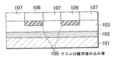
図1は、本発明の第1実施例における光電変換装置の断面構造を示す概念図である。 FIG. 1 is a conceptual diagram showing a cross-sectional structure of a photoelectric conversion device according to a first embodiment of the present invention.
ここで、101はSi等の半導体基体(一例としてN型)、102は基体全面に延在する埋め込み層(一例としてP型)、103は基体101と同一導電型のエピタキシャル層、106は埋め込み層102と同一導電型のウエル、107は基体101と同一導電型のウエルである。108が本発明の本質である、ウエル106と埋め込み層102の間の位置に挿入された、エピタキシャル層103と同一導電型のウエル分離用埋め込み層である。この、埋め込み層108の濃度をエピタキシャル層103の濃度より、十分高く設定し、且つ、ウエル106下面全面に配置することによって、ウエル106と埋め込み層102との間の電気的な分離を取ることが可能になる。
Here, 101 is a semiconductor substrate such as Si (N-type as an example), 102 is a buried layer (P-type as an example) extending over the entire surface of the substrate, 103 is an epitaxial layer of the same conductivity type as the
以下に、本発明による第1実施例の作製工程を説明する。 The manufacturing process of the first embodiment according to the present invention will be described below.
図2は、本発明の第1実施例における光電変換装置の各作製工程途中での断面構造を示す概念図である。 FIG. 2 is a conceptual diagram showing a cross-sectional structure in the middle of each manufacturing process of the photoelectric conversion device according to the first embodiment of the present invention.
最初にSi基体201を準備する。その比抵抗は15Ω・cmで、N型の導電性を持つ物である。埋め込み層202を形成するために、まず、緩衝膜として、熱酸化法によって、SiO2膜を150Å成長させる。次に、イオン注入法によって、ホウ素を8E13ions/cm2のドーズ量、及び60KeVの加速電圧で、Si基体201表面全体に打ち込む。次にこのイオンを活性化するために、900℃30分の熱処理を、窒素雰囲気中で行う。この後、緩衝膜のSiO2をフッ酸にて除去すれば、埋め込み層202が形成される。(図2−(a)参照)
次に、SiHCl3を用いたCVD法にて、Si基体201表面に、Siのエピタキシャル層203を成長させる。本実施例では、センサの分光感度を鑑み、厚さ4μm、比抵抗10Ω・cmでN型の物を成長させた。(図2−(b)参照)
本実施例とは別に、基体201に、直接エピタキシャル層203を堆積させ、しかる後に、高エネルギーイオン注入法等の手法を用いて、埋め込み層202を形成しても、図2−(b)のような構造体を形成することは、可能である。
First, the
Next, an Si
Even if the
次に、エピタキシャル層203の一部に、フォトリソグラフィ法によって、N型のウエル207の領域を規定し、その領域にリン及びホウ素を、イオン注入法にて打ち込んだ。本実施例での打ち込み条件は次のとおりである。まず、リンを6E12ions/cm2のドーズ量及び360KeVの加速電圧で、最も深い領域に打ち込み、中間領域には、リンを4E12ions/cm2のドーズ量及び180KeVで打ち込み、最表面には、ホウ素を3.8E12ions/cm2のドーズ量及び35KeVの加速電圧で打ち込んだ。最表面に打ち込んだホウ素は、このN型のウエル領域にこの後、作り込むPMOSトランジスタのチャネル領域の一部を兼ねている。(図2−(c)参照)
次に、エピタキシャル層203のN型のウエル207を形成しなかった領域の一部に、フォトリソグラフィ法によって、P型のウエル206の領域をレジスト209にて規定する。ここで、まず、P型のウエルを形成するための、ホウ素を、以下の3段階にて打ち込む。最も深い領域には、3E12ions/cm2のドーズ量及び250KeVの加速電圧で、中間領域には、2.5E12ions/cm2のドーズ量及び125KeVの加速電圧で、最表面には、3.8E12ions/cm2のドーズ量及び35KeVの加速電圧で、ホウ素を打ち込む。
Next, a region of the N-type well 207 was defined in a part of the
Next, a region of the P-
ここで、レジストを剥離せず、上記イオン注入法に連続してリンを1E12ions/cm2のドーズ量及び1.2MeVの加速電圧で打ち込めば、P型のウエル206の直下に、自己整合的にN型のウエル分離用埋め込み層208を形成することができる。(図2−(d)参照)
この後、レジスト209を除去すれば、図1のような、構造体を作ることができる。
Here, if the resist is not peeled off and phosphorus is implanted at a dose of 1E12 ions / cm 2 and an acceleration voltage of 1.2 MeV in succession to the above ion implantation method, self-aligned immediately below the P-
Thereafter, if the resist 209 is removed, a structure as shown in FIG. 1 can be formed.
上記、実施例の場合では、N型のウエル分離用埋め込み層208のピーク濃度は、1E16/cm3以上の値を取ることができ、エピタキシャル層203の濃度の2桁以上大きな値になる。
In the case of the above-described embodiment, the peak concentration of the N-type well isolation buried layer 208 can take a value of 1E16 / cm 3 or more, which is two or more orders of magnitude higher than the concentration of the
このことによって、P型の埋め込み層202とP型のウエル206との間に十分な電気的分離が取れるようになった。
As a result, sufficient electrical isolation can be obtained between the P-type buried
上記、構造形成後、公知の技術にて、フォトダイオード、及びMOSトランジスタを形成すれば、MOS型光電変換装置を単一基体の中に作り込むことができる。この時、特別なリソグラフィ工程は追加しておらず、リンのイオン注入工程の追加だけで、図1の構造体を形成している。 If the photodiode and the MOS transistor are formed by a known technique after the structure is formed, the MOS photoelectric conversion device can be built in a single substrate. At this time, a special lithography process is not added, and the structure of FIG. 1 is formed only by adding a phosphorus ion implantation process.
また、後工程でCCDを形成しても、図1の構造、及び図2に示す実施例の工程フローは有効で、MOS回路を集積化した、CCDに対しても、有用な役割を果たす。 Further, even if a CCD is formed in a later process, the structure shown in FIG. 1 and the process flow of the embodiment shown in FIG. 2 are effective and play a useful role for a CCD in which MOS circuits are integrated.
また、本発明の第2実施例は、フォトダイオード部と、周辺NMOSのP型のウエルを電気的に分離して形成した例である。 The second embodiment of the present invention is an example in which a photodiode portion and a peripheral NMOS P-type well are electrically separated.
図3は、本発明の第2実施例における光電変換装置のフォトダイオード部分と周辺MOSFET部分の断面構造を示す概念図である。 FIG. 3 is a conceptual diagram showing a cross-sectional structure of the photodiode portion and the peripheral MOSFET portion of the photoelectric conversion device according to the second embodiment of the present invention.
図3において、301は半導体基体、302は基体全面に延在する埋め込み層、303はエピタキシャル層、304はフォトダイオードの障壁拡散層、305はフォトダイオードの電荷蓄積拡散層、306は半導体基体と反対導電型のウエル、307は半導体基体と同一導電型のウエル、308は半導体基体と同一導電型のウエル分離用埋め込み層、309はNMOSのゲート電極、310は半導体基体と同一導電型のソース−ドレイン領域である。 In FIG. 3, 301 is a semiconductor substrate, 302 is a buried layer extending over the entire surface of the substrate, 303 is an epitaxial layer, 304 is a barrier diffusion layer of the photodiode, 305 is a charge storage diffusion layer of the photodiode, and 306 is opposite to the semiconductor substrate. Conductive well, 307 is a well of the same conductivity type as the semiconductor substrate, 308 is a well isolation buried layer of the same conductivity type as the semiconductor substrate, 309 is an NMOS gate electrode, and 310 is a source-drain of the same conductivity type as the semiconductor substrate. It is an area.
101,201,301,401 半導体基体
102,202,302,402 半導体基体全面に延在する埋め込み層
103,203,303,403 エピタキシャル層
304,404 フォトダイオードの障壁拡散層
305,405 フォトダイオードの電荷蓄積拡散層
106,206,306 半導体基体と反対導電型のウエル
107,207,307 半導体基体と同一導電型のウエル
108,208,308 半導体基体と同一導電型のウエル分離用埋め込み層
309 MOSFETのゲート電極
310 ソース−ドレイン領域
101, 201, 301, 401
Claims (6)
前記第1導電型の半導体基体上に配され、光電変換素子が配された第1の領域と駆動回路が配された第2の領域とを有する第1導電型のエピタキシャル層と、
前記第1導電型の半導体基体と前記第1導電型のエピタキシャル層との間に配され、前記第1導電型の半導体基体の全面に延在する第2導電型の第1の埋め込み層と、
前記第1導電型のエピタキシャル層内の前記第2の領域に配され、第1導電型のMOSFETのソース及びドレインを有する第2導電型の第1のウエルと、を有する光電変換装置において、
前記第2導電型の第1のウエルと前記第1導電型のエピタキシャル層との間に配され、前記第2導電型の第1のウエルの下部全面に接して延在し、前記第1導電型のエピタキシャル層よりも高い不純物濃度を有する第1導電型の第2の埋め込み層を有することを特徴とする光電変換装置。 A first conductivity type semiconductor substrate;
A first conductivity type epitaxial layer disposed on the first conductivity type semiconductor substrate and having a first region where a photoelectric conversion element is disposed and a second region where a drive circuit is disposed ;
A second conductive type first buried layer disposed between the first conductive type semiconductor substrate and the first conductive type epitaxial layer and extending over the entire surface of the first conductive type semiconductor substrate ;
In the first disposed on the second region of the conductivity type of the epitaxial layer, a photoelectric conversion device that perforated the first well of a second conductivity type having a source and a drain of the first conductivity type MOSFET, a,
The first conductivity type first well and the first conductivity type epitaxial layer are disposed between the first conductivity type first well and the first conductivity type first well, and extend in contact with the entire bottom surface of the second conductivity type first well. A photoelectric conversion device comprising a second buried layer of a first conductivity type having a higher impurity concentration than a type epitaxial layer .
複数の前記第2導電型の第1のウエルのそれぞれの下部に前記第1導電型の第2の埋め込み層が配されていることを特徴とする請求項1に記載の光電変換装置。 A plurality of first wells of the second conductivity type are arranged at intervals;
The photoelectric conversion device according to claim 1, wherein a plurality of said each of the lower portion of the second conductive type first well of a first conductivity type second buried layer of the are arranged.
前記第2導電型の第2のウエルと前記第1導電型のエピタキシャル層との間に配され、前記第2導電型の第2のウエルの下部全面に接して延在し、前記第1導電型のエピタキシャル層よりも高い不純物濃度を有する第1導電型の第3の埋め込み層と、 The first conductive type second well and the first conductive type epitaxial layer are disposed between the second conductive type second well and the lower surface of the second conductive type second well. A third buried layer of the first conductivity type having a higher impurity concentration than the epitaxial layer of the type;
前記第2導電型の第2のウエルに配され、前記第1導電型の第3の埋め込み層と接する前記光電変換素子の障壁拡散層とを有することを特徴とする請求項1乃至4のいずれか1項に記載の光電変換装置。 5. The device according to claim 1, further comprising a barrier diffusion layer of the photoelectric conversion element disposed in the second well of the second conductivity type and in contact with the third buried layer of the first conductivity type. The photoelectric conversion apparatus of Claim 1.
Priority Applications (2)
| Application Number | Priority Date | Filing Date | Title |
|---|---|---|---|
| JP2003321533A JP4510414B2 (en) | 2003-09-12 | 2003-09-12 | Photoelectric conversion device |
| US10/937,382 US7247899B2 (en) | 2003-09-12 | 2004-09-10 | Semiconductor device, photoelectric conversion device and method of manufacturing same |
Applications Claiming Priority (1)
| Application Number | Priority Date | Filing Date | Title |
|---|---|---|---|
| JP2003321533A JP4510414B2 (en) | 2003-09-12 | 2003-09-12 | Photoelectric conversion device |
Publications (3)
| Publication Number | Publication Date |
|---|---|
| JP2005093525A JP2005093525A (en) | 2005-04-07 |
| JP2005093525A5 JP2005093525A5 (en) | 2006-10-26 |
| JP4510414B2 true JP4510414B2 (en) | 2010-07-21 |
Family
ID=34269957
Family Applications (1)
| Application Number | Title | Priority Date | Filing Date |
|---|---|---|---|
| JP2003321533A Expired - Fee Related JP4510414B2 (en) | 2003-09-12 | 2003-09-12 | Photoelectric conversion device |
Country Status (2)
| Country | Link |
|---|---|
| US (1) | US7247899B2 (en) |
| JP (1) | JP4510414B2 (en) |
Families Citing this family (9)
| Publication number | Priority date | Publication date | Assignee | Title |
|---|---|---|---|---|
| US8513753B1 (en) * | 2004-09-14 | 2013-08-20 | Cypress Semiconductor Corporation | Photodiode having a buried well region |
| JP4667030B2 (en) * | 2004-12-10 | 2011-04-06 | キヤノン株式会社 | Semiconductor substrate for solid-state imaging device and manufacturing method thereof |
| JP5272281B2 (en) * | 2005-09-22 | 2013-08-28 | ソニー株式会社 | Solid-state imaging device, manufacturing method thereof, and camera |
| JP4679340B2 (en) * | 2005-11-11 | 2011-04-27 | 株式会社東芝 | Solid-state imaging device |
| KR101565750B1 (en) * | 2009-04-10 | 2015-11-05 | 삼성전자 주식회사 | High sensitivity image sensor |
| CN102479793B (en) * | 2010-11-29 | 2014-01-15 | 格科微电子(上海)有限公司 | Complementary metal-oxide-semiconductor (CMOS) image sensor and manufacture method thereof |
| JP5971565B2 (en) * | 2011-06-22 | 2016-08-17 | パナソニックIpマネジメント株式会社 | Solid-state imaging device |
| JP6355311B2 (en) | 2013-10-07 | 2018-07-11 | キヤノン株式会社 | Solid-state imaging device, manufacturing method thereof, and imaging system |
| JP2018139328A (en) * | 2018-06-05 | 2018-09-06 | キヤノン株式会社 | Solid-state imaging apparatus and imaging system |
Citations (10)
| Publication number | Priority date | Publication date | Assignee | Title |
|---|---|---|---|---|
| JPH03214666A (en) * | 1990-01-19 | 1991-09-19 | Toshiba Corp | Semiconductor device containing charge transfer device and manufacture thereof |
| JPH06205158A (en) * | 1993-01-01 | 1994-07-22 | Canon Inc | Solid-state image pickup device |
| JPH07254691A (en) * | 1994-03-15 | 1995-10-03 | Olympus Optical Co Ltd | Fabrication of solid state image sensor |
| JPH09246514A (en) * | 1996-03-12 | 1997-09-19 | Sharp Corp | Amplification type solid-state image sensing device |
| JP2000150848A (en) * | 1998-11-09 | 2000-05-30 | Toshiba Corp | Solid state imaging device |
| JP2000232214A (en) * | 1999-02-12 | 2000-08-22 | Nikon Corp | Semiconductor integrated circuit and solid-state imaging element |
| JP2002203954A (en) * | 2000-10-31 | 2002-07-19 | Sharp Corp | Light receiving element with built-in circuit |
| JP2002231917A (en) * | 2001-02-05 | 2002-08-16 | Hamamatsu Photonics Kk | Semiconductor light detection device |
| JP2002353146A (en) * | 2001-05-23 | 2002-12-06 | Sony Corp | System for producing semiconductor substrate and method for fabricating semiconductor device using that semiconductor substrate |
| JP2003142672A (en) * | 2001-10-31 | 2003-05-16 | Mitsubishi Electric Corp | Solid-state image sensor and method for manufacturing the same |
Family Cites Families (13)
| Publication number | Priority date | Publication date | Assignee | Title |
|---|---|---|---|---|
| US5260228A (en) | 1990-01-19 | 1993-11-09 | Kabushiki Kaisha Toshiba | Method of making a semiconductor device having a charge transfer device, MOSFETs, and bipolar transistors |
| JPH07109860B2 (en) | 1990-01-19 | 1995-11-22 | 株式会社東芝 | Semiconductor device including charge transfer device and manufacturing method thereof |
| JPH04176171A (en) | 1990-11-07 | 1992-06-23 | Sharp Corp | Solid-state image sensing device |
| US5248624A (en) * | 1991-08-23 | 1993-09-28 | Exar Corporation | Method of making isolated vertical pnp transistor in a complementary bicmos process with eeprom memory |
| JPH05226627A (en) * | 1992-02-10 | 1993-09-03 | Sharp Corp | Semiconductor device |
| US5302534A (en) * | 1992-03-02 | 1994-04-12 | Motorola, Inc. | Forming a vertical PNP transistor |
| JP3252432B2 (en) | 1992-03-19 | 2002-02-04 | 松下電器産業株式会社 | Semiconductor device and manufacturing method thereof |
| US5534069A (en) | 1992-07-23 | 1996-07-09 | Canon Kabushiki Kaisha | Method of treating active material |
| KR100192954B1 (en) * | 1996-07-18 | 1999-06-15 | 김광호 | Image pick-up device with a vertical transmission gate |
| EP0883187A1 (en) * | 1997-06-04 | 1998-12-09 | Interuniversitair Micro-Elektronica Centrum Vzw | A detector for electromagnetic radiation, pixel structure with high sensitivity using such detector and method of manufacturing such detector |
| JP4419238B2 (en) * | 1999-12-27 | 2010-02-24 | ソニー株式会社 | Solid-state imaging device and manufacturing method thereof |
| KR100867574B1 (en) * | 2002-05-09 | 2008-11-10 | 페어차일드코리아반도체 주식회사 | Power device and method for manufacturing the same |
| US7110028B1 (en) * | 2002-08-13 | 2006-09-19 | Foveon, Inc. | Electronic shutter using buried layers and active pixel sensor and array employing same |
-
2003
- 2003-09-12 JP JP2003321533A patent/JP4510414B2/en not_active Expired - Fee Related
-
2004
- 2004-09-10 US US10/937,382 patent/US7247899B2/en not_active Expired - Fee Related
Patent Citations (10)
| Publication number | Priority date | Publication date | Assignee | Title |
|---|---|---|---|---|
| JPH03214666A (en) * | 1990-01-19 | 1991-09-19 | Toshiba Corp | Semiconductor device containing charge transfer device and manufacture thereof |
| JPH06205158A (en) * | 1993-01-01 | 1994-07-22 | Canon Inc | Solid-state image pickup device |
| JPH07254691A (en) * | 1994-03-15 | 1995-10-03 | Olympus Optical Co Ltd | Fabrication of solid state image sensor |
| JPH09246514A (en) * | 1996-03-12 | 1997-09-19 | Sharp Corp | Amplification type solid-state image sensing device |
| JP2000150848A (en) * | 1998-11-09 | 2000-05-30 | Toshiba Corp | Solid state imaging device |
| JP2000232214A (en) * | 1999-02-12 | 2000-08-22 | Nikon Corp | Semiconductor integrated circuit and solid-state imaging element |
| JP2002203954A (en) * | 2000-10-31 | 2002-07-19 | Sharp Corp | Light receiving element with built-in circuit |
| JP2002231917A (en) * | 2001-02-05 | 2002-08-16 | Hamamatsu Photonics Kk | Semiconductor light detection device |
| JP2002353146A (en) * | 2001-05-23 | 2002-12-06 | Sony Corp | System for producing semiconductor substrate and method for fabricating semiconductor device using that semiconductor substrate |
| JP2003142672A (en) * | 2001-10-31 | 2003-05-16 | Mitsubishi Electric Corp | Solid-state image sensor and method for manufacturing the same |
Also Published As
| Publication number | Publication date |
|---|---|
| JP2005093525A (en) | 2005-04-07 |
| US20050056905A1 (en) | 2005-03-17 |
| US7247899B2 (en) | 2007-07-24 |
Similar Documents
| Publication | Publication Date | Title |
|---|---|---|
| JP7279277B2 (en) | Multiple shield trench gate FET | |
| JPH09120995A (en) | Semiconductor device and its manufacture | |
| JP2008085134A (en) | Semiconductor device and its manufacturing method | |
| JP2004241613A (en) | Semiconductor device | |
| JP4510414B2 (en) | Photoelectric conversion device | |
| JP2006253376A (en) | Semiconductor device and its manufacturing method | |
| JPH0824144B2 (en) | Method for manufacturing semiconductor device | |
| JPH077773B2 (en) | Method for manufacturing semiconductor device | |
| JPS59111359A (en) | Method of producing semiconductor structure | |
| JP2745228B2 (en) | Semiconductor device and manufacturing method thereof | |
| JP2009130021A (en) | Lateral mos transistor and method of manufacturing the same | |
| JP2006186392A (en) | Semiconductor device and its manufacturing method | |
| JP2004031805A (en) | Semiconductor device and its manufacturing method | |
| KR20060023009A (en) | High voltage transistor and method for fabricating the same | |
| JPH08316335A (en) | Semiconductor device and fabrication thereof | |
| JP2949745B2 (en) | Method of manufacturing vertical MOS field effect transistor | |
| JP4166031B2 (en) | MOS semiconductor device and manufacturing method thereof | |
| JP4147829B2 (en) | Method for manufacturing solid-state imaging device | |
| JP2005044948A (en) | Semiconductor device and manufacturing method thereof | |
| JP2007053399A (en) | Semiconductor device | |
| JP2003303959A (en) | Vertical mos semiconductor device and manufacturing method thereof | |
| JPH10163338A (en) | Semiconductor device and its manufacturing method | |
| JP6668600B2 (en) | Solid-state imaging device and method of manufacturing the same | |
| JP4118196B2 (en) | Semiconductor element, manufacturing method thereof and semiconductor device | |
| JP2611450B2 (en) | Semiconductor integrated circuit and manufacturing method thereof |
Legal Events
| Date | Code | Title | Description |
|---|---|---|---|
| A521 | Request for written amendment filed |
Free format text: JAPANESE INTERMEDIATE CODE: A523 Effective date: 20060911 |
|
| A621 | Written request for application examination |
Free format text: JAPANESE INTERMEDIATE CODE: A621 Effective date: 20060911 |
|
| RD04 | Notification of resignation of power of attorney |
Free format text: JAPANESE INTERMEDIATE CODE: A7424 Effective date: 20080207 |
|
| RD03 | Notification of appointment of power of attorney |
Free format text: JAPANESE INTERMEDIATE CODE: A7423 Effective date: 20090326 |
|
| RD05 | Notification of revocation of power of attorney |
Free format text: JAPANESE INTERMEDIATE CODE: A7425 Effective date: 20090427 |
|
| A977 | Report on retrieval |
Free format text: JAPANESE INTERMEDIATE CODE: A971007 Effective date: 20091109 |
|
| A131 | Notification of reasons for refusal |
Free format text: JAPANESE INTERMEDIATE CODE: A131 Effective date: 20091113 |
|
| A521 | Request for written amendment filed |
Free format text: JAPANESE INTERMEDIATE CODE: A523 Effective date: 20100112 |
|
| TRDD | Decision of grant or rejection written | ||
| A01 | Written decision to grant a patent or to grant a registration (utility model) |
Free format text: JAPANESE INTERMEDIATE CODE: A01 Effective date: 20100427 |
|
| A01 | Written decision to grant a patent or to grant a registration (utility model) |
Free format text: JAPANESE INTERMEDIATE CODE: A01 |
|
| A61 | First payment of annual fees (during grant procedure) |
Free format text: JAPANESE INTERMEDIATE CODE: A61 Effective date: 20100430 |
|
| FPAY | Renewal fee payment (event date is renewal date of database) |
Free format text: PAYMENT UNTIL: 20130514 Year of fee payment: 3 |
|
| R150 | Certificate of patent or registration of utility model |
Free format text: JAPANESE INTERMEDIATE CODE: R150 |
|
| FPAY | Renewal fee payment (event date is renewal date of database) |
Free format text: PAYMENT UNTIL: 20140514 Year of fee payment: 4 |
|
| LAPS | Cancellation because of no payment of annual fees |