JP5998521B2 - 不揮発性半導体メモリー及び不揮発性半導体メモリーの製造方法 - Google Patents
不揮発性半導体メモリー及び不揮発性半導体メモリーの製造方法 Download PDFInfo
- Publication number
- JP5998521B2 JP5998521B2 JP2012041221A JP2012041221A JP5998521B2 JP 5998521 B2 JP5998521 B2 JP 5998521B2 JP 2012041221 A JP2012041221 A JP 2012041221A JP 2012041221 A JP2012041221 A JP 2012041221A JP 5998521 B2 JP5998521 B2 JP 5998521B2
- Authority
- JP
- Japan
- Prior art keywords
- oxide film
- silicon
- nitride film
- silicon oxide
- silicon nitride
- Prior art date
- Legal status (The legal status is an assumption and is not a legal conclusion. Google has not performed a legal analysis and makes no representation as to the accuracy of the status listed.)
- Active
Links
- 239000004065 semiconductor Substances 0.000 title claims description 76
- 238000004519 manufacturing process Methods 0.000 title claims description 34
- 238000000034 method Methods 0.000 title claims description 33
- 229910052581 Si3N4 Inorganic materials 0.000 claims description 143
- HQVNEWCFYHHQES-UHFFFAOYSA-N silicon nitride Chemical compound N12[Si]34N5[Si]62N3[Si]51N64 HQVNEWCFYHHQES-UHFFFAOYSA-N 0.000 claims description 141
- 229910052814 silicon oxide Inorganic materials 0.000 claims description 135
- VYPSYNLAJGMNEJ-UHFFFAOYSA-N Silicium dioxide Chemical compound O=[Si]=O VYPSYNLAJGMNEJ-UHFFFAOYSA-N 0.000 claims description 132
- XUIMIQQOPSSXEZ-UHFFFAOYSA-N Silicon Chemical compound [Si] XUIMIQQOPSSXEZ-UHFFFAOYSA-N 0.000 claims description 61
- 229910052710 silicon Inorganic materials 0.000 claims description 61
- 239000010703 silicon Substances 0.000 claims description 61
- 239000000758 substrate Substances 0.000 claims description 59
- 229910021332 silicide Inorganic materials 0.000 claims description 21
- FVBUAEGBCNSCDD-UHFFFAOYSA-N silicide(4-) Chemical group [Si-4] FVBUAEGBCNSCDD-UHFFFAOYSA-N 0.000 claims description 19
- 238000005530 etching Methods 0.000 claims description 6
- 238000000059 patterning Methods 0.000 claims description 5
- 239000010408 film Substances 0.000 description 255
- 230000008569 process Effects 0.000 description 23
- 239000010410 layer Substances 0.000 description 19
- 230000015654 memory Effects 0.000 description 15
- 238000009792 diffusion process Methods 0.000 description 9
- 238000009825 accumulation Methods 0.000 description 8
- 238000000137 annealing Methods 0.000 description 6
- 239000010941 cobalt Substances 0.000 description 6
- 229910017052 cobalt Inorganic materials 0.000 description 6
- 238000001312 dry etching Methods 0.000 description 5
- 230000004913 activation Effects 0.000 description 4
- GUTLYIVDDKVIGB-UHFFFAOYSA-N cobalt atom Chemical compound [Co] GUTLYIVDDKVIGB-UHFFFAOYSA-N 0.000 description 4
- 230000007423 decrease Effects 0.000 description 4
- 230000000694 effects Effects 0.000 description 4
- 238000010438 heat treatment Methods 0.000 description 4
- 239000012535 impurity Substances 0.000 description 4
- 150000004767 nitrides Chemical class 0.000 description 4
- 230000008901 benefit Effects 0.000 description 3
- 230000008859 change Effects 0.000 description 3
- 239000011229 interlayer Substances 0.000 description 3
- 238000004544 sputter deposition Methods 0.000 description 3
- -1 Silicon Oxide Nitride Chemical class 0.000 description 2
- 230000004888 barrier function Effects 0.000 description 2
- 230000015572 biosynthetic process Effects 0.000 description 2
- 239000000470 constituent Substances 0.000 description 2
- 238000010586 diagram Methods 0.000 description 2
- 230000014759 maintenance of location Effects 0.000 description 2
- 229910021420 polycrystalline silicon Inorganic materials 0.000 description 2
- 229920005591 polysilicon Polymers 0.000 description 2
- 229910004298 SiO 2 Inorganic materials 0.000 description 1
- 229910020286 SiOxNy Inorganic materials 0.000 description 1
- 238000000277 atomic layer chemical vapour deposition Methods 0.000 description 1
- QVGXLLKOCUKJST-UHFFFAOYSA-N atomic oxygen Chemical compound [O] QVGXLLKOCUKJST-UHFFFAOYSA-N 0.000 description 1
- 238000009413 insulation Methods 0.000 description 1
- 238000005468 ion implantation Methods 0.000 description 1
- 150000002500 ions Chemical class 0.000 description 1
- 238000002955 isolation Methods 0.000 description 1
- 230000003446 memory effect Effects 0.000 description 1
- 230000006386 memory function Effects 0.000 description 1
- 229910044991 metal oxide Inorganic materials 0.000 description 1
- 230000001590 oxidative effect Effects 0.000 description 1
- 229910052760 oxygen Inorganic materials 0.000 description 1
- 239000001301 oxygen Substances 0.000 description 1
- 239000010409 thin film Substances 0.000 description 1
- 229910021341 titanium silicide Inorganic materials 0.000 description 1
- WFKWXMTUELFFGS-UHFFFAOYSA-N tungsten Chemical compound [W] WFKWXMTUELFFGS-UHFFFAOYSA-N 0.000 description 1
- 239000010937 tungsten Substances 0.000 description 1
- 229910052721 tungsten Inorganic materials 0.000 description 1
Images


Classifications
-
- H—ELECTRICITY
- H01—ELECTRIC ELEMENTS
- H01L—SEMICONDUCTOR DEVICES NOT COVERED BY CLASS H10
- H01L29/00—Semiconductor devices adapted for rectifying, amplifying, oscillating or switching, or capacitors or resistors with at least one potential-jump barrier or surface barrier, e.g. PN junction depletion layer or carrier concentration layer; Details of semiconductor bodies or of electrodes thereof ; Multistep manufacturing processes therefor
- H01L29/40—Electrodes ; Multistep manufacturing processes therefor
- H01L29/43—Electrodes ; Multistep manufacturing processes therefor characterised by the materials of which they are formed
- H01L29/49—Metal-insulator-semiconductor electrodes, e.g. gates of MOSFET
- H01L29/51—Insulating materials associated therewith
- H01L29/511—Insulating materials associated therewith with a compositional variation, e.g. multilayer structures
- H01L29/512—Insulating materials associated therewith with a compositional variation, e.g. multilayer structures the variation being parallel to the channel plane
-
- H—ELECTRICITY
- H10—SEMICONDUCTOR DEVICES; ELECTRIC SOLID-STATE DEVICES NOT OTHERWISE PROVIDED FOR
- H10B—ELECTRONIC MEMORY DEVICES
- H10B53/00—Ferroelectric RAM [FeRAM] devices comprising ferroelectric memory capacitors
- H10B53/30—Ferroelectric RAM [FeRAM] devices comprising ferroelectric memory capacitors characterised by the memory core region
-
- H—ELECTRICITY
- H01—ELECTRIC ELEMENTS
- H01L—SEMICONDUCTOR DEVICES NOT COVERED BY CLASS H10
- H01L29/00—Semiconductor devices adapted for rectifying, amplifying, oscillating or switching, or capacitors or resistors with at least one potential-jump barrier or surface barrier, e.g. PN junction depletion layer or carrier concentration layer; Details of semiconductor bodies or of electrodes thereof ; Multistep manufacturing processes therefor
- H01L29/40—Electrodes ; Multistep manufacturing processes therefor
- H01L29/43—Electrodes ; Multistep manufacturing processes therefor characterised by the materials of which they are formed
- H01L29/49—Metal-insulator-semiconductor electrodes, e.g. gates of MOSFET
- H01L29/51—Insulating materials associated therewith
- H01L29/511—Insulating materials associated therewith with a compositional variation, e.g. multilayer structures
- H01L29/513—Insulating materials associated therewith with a compositional variation, e.g. multilayer structures the variation being perpendicular to the channel plane
-
- H—ELECTRICITY
- H01—ELECTRIC ELEMENTS
- H01L—SEMICONDUCTOR DEVICES NOT COVERED BY CLASS H10
- H01L21/00—Processes or apparatus adapted for the manufacture or treatment of semiconductor or solid state devices or of parts thereof
- H01L21/02—Manufacture or treatment of semiconductor devices or of parts thereof
- H01L21/02104—Forming layers
- H01L21/02107—Forming insulating materials on a substrate
- H01L21/02109—Forming insulating materials on a substrate characterised by the type of layer, e.g. type of material, porous/non-porous, pre-cursors, mixtures or laminates
- H01L21/02112—Forming insulating materials on a substrate characterised by the type of layer, e.g. type of material, porous/non-porous, pre-cursors, mixtures or laminates characterised by the material of the layer
- H01L21/02123—Forming insulating materials on a substrate characterised by the type of layer, e.g. type of material, porous/non-porous, pre-cursors, mixtures or laminates characterised by the material of the layer the material containing silicon
- H01L21/02164—Forming insulating materials on a substrate characterised by the type of layer, e.g. type of material, porous/non-porous, pre-cursors, mixtures or laminates characterised by the material of the layer the material containing silicon the material being a silicon oxide, e.g. SiO2
-
- H—ELECTRICITY
- H01—ELECTRIC ELEMENTS
- H01L—SEMICONDUCTOR DEVICES NOT COVERED BY CLASS H10
- H01L21/00—Processes or apparatus adapted for the manufacture or treatment of semiconductor or solid state devices or of parts thereof
- H01L21/02—Manufacture or treatment of semiconductor devices or of parts thereof
- H01L21/02104—Forming layers
- H01L21/02107—Forming insulating materials on a substrate
- H01L21/02109—Forming insulating materials on a substrate characterised by the type of layer, e.g. type of material, porous/non-porous, pre-cursors, mixtures or laminates
- H01L21/02112—Forming insulating materials on a substrate characterised by the type of layer, e.g. type of material, porous/non-porous, pre-cursors, mixtures or laminates characterised by the material of the layer
- H01L21/02123—Forming insulating materials on a substrate characterised by the type of layer, e.g. type of material, porous/non-porous, pre-cursors, mixtures or laminates characterised by the material of the layer the material containing silicon
- H01L21/0217—Forming insulating materials on a substrate characterised by the type of layer, e.g. type of material, porous/non-porous, pre-cursors, mixtures or laminates characterised by the material of the layer the material containing silicon the material being a silicon nitride not containing oxygen, e.g. SixNy or SixByNz
-
- H—ELECTRICITY
- H01—ELECTRIC ELEMENTS
- H01L—SEMICONDUCTOR DEVICES NOT COVERED BY CLASS H10
- H01L29/00—Semiconductor devices adapted for rectifying, amplifying, oscillating or switching, or capacitors or resistors with at least one potential-jump barrier or surface barrier, e.g. PN junction depletion layer or carrier concentration layer; Details of semiconductor bodies or of electrodes thereof ; Multistep manufacturing processes therefor
- H01L29/40—Electrodes ; Multistep manufacturing processes therefor
- H01L29/401—Multistep manufacturing processes
- H01L29/4011—Multistep manufacturing processes for data storage electrodes
- H01L29/40117—Multistep manufacturing processes for data storage electrodes the electrodes comprising a charge-trapping insulator
-
- H—ELECTRICITY
- H01—ELECTRIC ELEMENTS
- H01L—SEMICONDUCTOR DEVICES NOT COVERED BY CLASS H10
- H01L29/00—Semiconductor devices adapted for rectifying, amplifying, oscillating or switching, or capacitors or resistors with at least one potential-jump barrier or surface barrier, e.g. PN junction depletion layer or carrier concentration layer; Details of semiconductor bodies or of electrodes thereof ; Multistep manufacturing processes therefor
- H01L29/40—Electrodes ; Multistep manufacturing processes therefor
- H01L29/43—Electrodes ; Multistep manufacturing processes therefor characterised by the materials of which they are formed
- H01L29/49—Metal-insulator-semiconductor electrodes, e.g. gates of MOSFET
- H01L29/51—Insulating materials associated therewith
- H01L29/518—Insulating materials associated therewith the insulating material containing nitrogen, e.g. nitride, oxynitride, nitrogen-doped material
-
- H—ELECTRICITY
- H01—ELECTRIC ELEMENTS
- H01L—SEMICONDUCTOR DEVICES NOT COVERED BY CLASS H10
- H01L29/00—Semiconductor devices adapted for rectifying, amplifying, oscillating or switching, or capacitors or resistors with at least one potential-jump barrier or surface barrier, e.g. PN junction depletion layer or carrier concentration layer; Details of semiconductor bodies or of electrodes thereof ; Multistep manufacturing processes therefor
- H01L29/66—Types of semiconductor device ; Multistep manufacturing processes therefor
- H01L29/66007—Multistep manufacturing processes
- H01L29/66075—Multistep manufacturing processes of devices having semiconductor bodies comprising group 14 or group 13/15 materials
- H01L29/66227—Multistep manufacturing processes of devices having semiconductor bodies comprising group 14 or group 13/15 materials the devices being controllable only by the electric current supplied or the electric potential applied, to an electrode which does not carry the current to be rectified, amplified or switched, e.g. three-terminal devices
- H01L29/66409—Unipolar field-effect transistors
- H01L29/66477—Unipolar field-effect transistors with an insulated gate, i.e. MISFET
- H01L29/66825—Unipolar field-effect transistors with an insulated gate, i.e. MISFET with a floating gate
-
- H—ELECTRICITY
- H01—ELECTRIC ELEMENTS
- H01L—SEMICONDUCTOR DEVICES NOT COVERED BY CLASS H10
- H01L29/00—Semiconductor devices adapted for rectifying, amplifying, oscillating or switching, or capacitors or resistors with at least one potential-jump barrier or surface barrier, e.g. PN junction depletion layer or carrier concentration layer; Details of semiconductor bodies or of electrodes thereof ; Multistep manufacturing processes therefor
- H01L29/66—Types of semiconductor device ; Multistep manufacturing processes therefor
- H01L29/66007—Multistep manufacturing processes
- H01L29/66075—Multistep manufacturing processes of devices having semiconductor bodies comprising group 14 or group 13/15 materials
- H01L29/66227—Multistep manufacturing processes of devices having semiconductor bodies comprising group 14 or group 13/15 materials the devices being controllable only by the electric current supplied or the electric potential applied, to an electrode which does not carry the current to be rectified, amplified or switched, e.g. three-terminal devices
- H01L29/66409—Unipolar field-effect transistors
- H01L29/66477—Unipolar field-effect transistors with an insulated gate, i.e. MISFET
- H01L29/66833—Unipolar field-effect transistors with an insulated gate, i.e. MISFET with a charge trapping gate insulator, e.g. MNOS transistors
-
- H—ELECTRICITY
- H01—ELECTRIC ELEMENTS
- H01L—SEMICONDUCTOR DEVICES NOT COVERED BY CLASS H10
- H01L29/00—Semiconductor devices adapted for rectifying, amplifying, oscillating or switching, or capacitors or resistors with at least one potential-jump barrier or surface barrier, e.g. PN junction depletion layer or carrier concentration layer; Details of semiconductor bodies or of electrodes thereof ; Multistep manufacturing processes therefor
- H01L29/66—Types of semiconductor device ; Multistep manufacturing processes therefor
- H01L29/68—Types of semiconductor device ; Multistep manufacturing processes therefor controllable by only the electric current supplied, or only the electric potential applied, to an electrode which does not carry the current to be rectified, amplified or switched
- H01L29/76—Unipolar devices, e.g. field effect transistors
- H01L29/772—Field effect transistors
- H01L29/78—Field effect transistors with field effect produced by an insulated gate
- H01L29/788—Field effect transistors with field effect produced by an insulated gate with floating gate
- H01L29/7881—Programmable transistors with only two possible levels of programmation
-
- H—ELECTRICITY
- H01—ELECTRIC ELEMENTS
- H01L—SEMICONDUCTOR DEVICES NOT COVERED BY CLASS H10
- H01L29/00—Semiconductor devices adapted for rectifying, amplifying, oscillating or switching, or capacitors or resistors with at least one potential-jump barrier or surface barrier, e.g. PN junction depletion layer or carrier concentration layer; Details of semiconductor bodies or of electrodes thereof ; Multistep manufacturing processes therefor
- H01L29/66—Types of semiconductor device ; Multistep manufacturing processes therefor
- H01L29/68—Types of semiconductor device ; Multistep manufacturing processes therefor controllable by only the electric current supplied, or only the electric potential applied, to an electrode which does not carry the current to be rectified, amplified or switched
- H01L29/76—Unipolar devices, e.g. field effect transistors
- H01L29/772—Field effect transistors
- H01L29/78—Field effect transistors with field effect produced by an insulated gate
- H01L29/792—Field effect transistors with field effect produced by an insulated gate with charge trapping gate insulator, e.g. MNOS-memory transistors
-
- H—ELECTRICITY
- H10—SEMICONDUCTOR DEVICES; ELECTRIC SOLID-STATE DEVICES NOT OTHERWISE PROVIDED FOR
- H10B—ELECTRONIC MEMORY DEVICES
- H10B53/00—Ferroelectric RAM [FeRAM] devices comprising ferroelectric memory capacitors
- H10B53/20—Ferroelectric RAM [FeRAM] devices comprising ferroelectric memory capacitors characterised by the three-dimensional arrangements, e.g. with cells on different height levels
Description
本適用例にかかる不揮発性半導体メモリーは、シリコン基板と、第1のシリコン酸化膜と、第2のシリコン酸化膜と、第1のシリコン窒化膜と、第2のシリコン窒化膜と、を含み、前記第1のシリコン酸化膜は、前記シリコン基板上に積層され、前記第1のシリコン窒化膜は、前記第1のシリコン酸化膜上に積層され、前記第2のシリコン酸化膜は、前記第1のシリコン窒化膜上に積層され、前記第2のシリコン窒化膜は、第1の部分が前記第1のシリコン窒化膜に接すると共に第2の部分が前記シリコン基板に接するように積層されていることを特徴とする。
本適用例にかかる不揮発性半導体メモリーは、シリコン基板と、第1のシリコン酸化膜と、第2のシリコン酸化膜と、第3のシリコン酸化膜と、第1のシリコン窒化膜と、第2のシリコン窒化膜と、を含み、前記第1のシリコン酸化膜は、前記シリコン基板上に積層され、前記第1のシリコン窒化膜は、前記第1のシリコン酸化膜上に積層され、前記第2のシリコン酸化膜は、前記第1のシリコン窒化膜上に積層され、前記第3のシリコン酸化膜の厚さは、前記第1のシリコン酸化膜の厚さよりも薄く、前記第2のシリコン窒化膜は、第1の部分が前記第1のシリコン窒化膜に接すると共に第2の部分が前記第3のシリコン酸化膜を介して前記シリコン基板に接していることを特徴とする。
上記適用例にかかる不揮発性半導体メモリーにおいて、更に、前記シリコン基板内にシリサイド領域を含み、前記シリサイド領域は、前記第2のシリコン窒化膜の第2の部分に接することが好ましい。
上記適用例にかかる不揮発性半導体メモリーにおいて、更に、前記第2のシリコン酸化膜上に第1の電極を有し、前記第2のシリコン窒化膜の第3の部分が前記第1の電極に接していることが好ましい。
上記適用例にかかる不揮発性半導体メモリーにおいて、前記第3のシリコン酸化膜は、厚さが22Å以下であることが好ましい。
上記適用例にかかる不揮発性半導体メモリーにおいて、前記第2のシリコン窒化膜は、厚さが45Å以上であることが好ましい。
本適用例にかかる不揮発性半導体メモリーの製造方法は、シリコン基板上に、第1のシリコン酸化膜を成膜する第1の工程と、前記第1のシリコン酸化膜上に、第1のシリコン窒化膜を成膜する第2の工程と、前記第1のシリコン窒化膜上に、第2のシリコン酸化膜を成膜する第3の工程と、前記第1のシリコン酸化膜、前記第1のシリコン窒化膜及び第2のシリコン酸化膜を所定の形状にパターニングする第4の工程と、前記第4の工程の後に第2のシリコン窒化膜を成膜する第5の工程と、を含み、前記第4の工程において、前記第1のシリコン窒化膜及び前記シリコン基板が露出され、前記第5の工程において、前記第1のシリコン窒化膜と前記第2のシリコン窒化膜とが接することを特徴とする。
上記適用例にかかる不揮発性半導体メモリーの製造方法において、前記第4の工程と前記第5の工程の間の第6の工程において、前記シリコン基板が露出された領域に第3のシリコン酸化膜が形成されていてもよい。
本適用例にかかる不揮発性半導体メモリーの製造方法は、シリコン基板上に、第1のシリコン酸化膜を成膜する第1の工程と、前記第1のシリコン酸化膜上に、第1のシリコン窒化膜を成膜する第2の工程と、前記第1のシリコン窒化膜上に、第2のシリコン酸化膜を成膜する第3の工程と、前記第1のシリコン酸化膜、前記第1のシリコン窒化膜及び第2のシリコン酸化膜を所定の形状にパターニングする第4の工程と、前記第4の工程の後に第2のシリコン窒化膜を成膜する第5の工程と、を含み、前記第4の工程において、前記第1のシリコン窒化膜が露出され、前記第1のシリコン酸化膜をエッチングすることで前記第1のシリコン酸化膜より膜厚が薄い第3のシリコン酸化膜が形成され、前記第5の工程において、前記第1のシリコン窒化膜と前記第2のシリコン窒化膜とが接することを特徴とする。
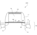
図1に本願発明を適用した不揮発性半導体メモリー100の断面図を示す。不揮発性半導体メモリー100は、シリコン基板12を用いて形成され、第1電極10、サイドウォール11、ソース領域/ドレイン領域13、シリサイド領域14、シリサイド層15、第1シリコン酸化膜20、第1シリコン窒化膜21、第2シリコン酸化膜22及び第2シリコン窒化膜23を有する。第1電極10としては、例えばポリシリコン膜、サイドウォール11としては、例えばシリコン酸化膜が用いられる。ソース領域/ドレイン領域13及びシリサイド領域14は、シリコン基板12内に形成された領域である。シリサイドは、例えばコバルトシリサイドやチタンシリサイドが用いられる。また、メモリー機能のためのトラップ層は、第1シリコン酸化膜20、第1シリコン窒化膜21及び第2シリコン酸化膜22から構成されるONO構造である。第2シリコン窒化膜23は、第1シリコン窒化膜21及びシリコン基板12に接している。以後、特に断りがない限り、シリコン基板12は、ソース領域/ドレイン領域13及びシリサイド領域14を含む意味で記載する。
本実施形態も含め、以降に記載する実施形態の説明において、第1実施形態と同様の構成要素については同じ番号を付与し、その説明を省略する。
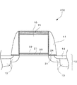
図3に本願発明を適用した不揮発性半導体メモリー300の断面図を示す。不揮発性半導体メモリー300は、シリコン基板12及び第1電極10に接する第2シリコン窒化膜24を有する。サイドウォール11は、第2シリコン窒化膜24を覆うように形成されている。上記した第2シリコン窒化膜23と同様に、第2シリコン窒化膜24の厚さは45Å以上であることが好ましい。
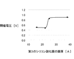
図4に本願発明を適用した不揮発性半導体メモリー400の断面図を示す。不揮発性半導体メモリー400は、不揮発性半導体メモリー300の構成要素に第3シリコン酸化膜31を付加したものである。第2シリコン窒化膜24は、第3シリコン酸化膜31を介してシリコン基板12に接している。第3シリコン酸化膜31の厚さは、第1シリコン酸化膜20の厚さよりも薄く形成されている。これにより、第1シリコン酸化膜20が第1シリコン窒化膜21の電荷を拡散させることに対する障壁となっても、第3シリコン酸化膜31を介して該電荷を拡散させることができる。上記した第3シリコン酸化膜30と同様に、第3シリコン酸化膜31の厚さは22Å以下であることが好ましい。
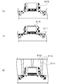
本実施形態は、本発明にかかるONO構造を有する不揮発性半導体メモリーの製造方法の1例を説明するものである。具体的には、上述した不揮発性半導体メモリー300若しくは400の製造方法となる。図7及び図8に、製造過程における素子の断面図の模式図を示す。尚、図に示しているのは、不揮発性半導体メモリーの部分のみであり、他の種類の素子の形成も同時に行われている。また、該不揮発性半導体メモリーを形成する領域をONO領域と呼ぶことにする。
Claims (6)
- 不揮発性半導体メモリーであって、
シリコン基板と、
第1のシリコン酸化膜と、
第2のシリコン酸化膜と、
第3のシリコン酸化膜と、
第1のシリコン窒化膜と、
第2のシリコン窒化膜と、を含み、
前記第1のシリコン酸化膜および前記第3のシリコン酸化膜は、前記シリコン基板上に積層され、
前記第1のシリコン窒化膜は、前記第1のシリコン酸化膜上に積層され、
前記第2のシリコン酸化膜は、前記第1のシリコン窒化膜上に積層され、
前記第3のシリコン酸化膜の厚さは、前記第1のシリコン酸化膜の厚さよりも薄く、
前記第2のシリコン窒化膜は、第1の部分が前記第1のシリコン窒化膜に接すると共に第2の部分が前記第3のシリコン酸化膜に接しており、
前記第3のシリコン酸化膜は、厚さが0Åより大きく22Å以下であることを特徴とする不揮発性半導体メモリー。 - 更に、前記シリコン基板内にシリサイド領域を含み、
前記シリサイド領域は、前記第3のシリコン酸化膜に接することを特徴する請求項1に記載の不揮発性半導体メモリー。 - 更に、前記第2のシリコン酸化膜上に第1の電極を有し、
前記第2のシリコン窒化膜の第3の部分が前記第1の電極に接していることを特徴とする請求項1又は2に記載の不揮発性半導体メモリー。 - 前記第2のシリコン窒化膜は、厚さが45Å以上であることを特徴とする請求項1乃至3のいずれか一項に記載の不揮発性半導体メモリー。
- 不揮発性半導体メモリーの製造方法であって、
シリコン基板上に、第1のシリコン酸化膜を成膜する第1の工程と、
前記第1のシリコン酸化膜上に、第1のシリコン窒化膜を成膜する第2の工程と、
前記第1のシリコン窒化膜上に、第2のシリコン酸化膜を成膜する第3の工程と、
前記第1のシリコン酸化膜、前記第1のシリコン窒化膜及び第2のシリコン酸化膜を所定の形状にパターニングする第4の工程と、
前記第4の工程の後に第2のシリコン窒化膜を成膜する第5の工程と、を含み、
前記第4の工程において、前記第1のシリコン窒化膜及び前記シリコン基板が露出され、
前記第4の工程と前記第5の工程の間の第6の工程において、前記シリコン基板が露出された領域に前記第1のシリコン酸化膜より膜厚が薄い第3のシリコン酸化膜が形成され、
前記第3のシリコン酸化膜は、厚さが0Åより大きく22Å以下であり、
前記第5の工程において、前記第1のシリコン窒化膜と前記第2のシリコン窒化膜とが接することを特徴とする不揮発性半導体メモリーの製造方法。 - 不揮発性半導体メモリーの製造方法であって、
シリコン基板上に、第1のシリコン酸化膜を成膜する第1の工程と、
前記第1のシリコン酸化膜上に、第1のシリコン窒化膜を成膜する第2の工程と、
前記第1のシリコン窒化膜上に、第2のシリコン酸化膜を成膜する第3の工程と、
前記第1のシリコン酸化膜、前記第1のシリコン窒化膜及び第2のシリコン酸化膜を所定の形状にパターニングする第4の工程と、
前記第4の工程の後に第2のシリコン窒化膜を成膜する第5の工程と、を含み、
前記第4の工程において、前記第1のシリコン窒化膜が露出され、前記第1のシリコン酸化膜をエッチングすることで前記第1のシリコン酸化膜より膜厚が薄い第3のシリコン酸化膜が形成され、
前記第3のシリコン酸化膜は、厚さが0Åより大きく22Å以下であり、
前記第5の工程において、前記第1のシリコン窒化膜と前記第2のシリコン窒化膜とが接することを特徴とする不揮発性半導体メモリーの製造方法。
Priority Applications (6)
| Application Number | Priority Date | Filing Date | Title |
|---|---|---|---|
| JP2012041221A JP5998521B2 (ja) | 2012-02-28 | 2012-02-28 | 不揮発性半導体メモリー及び不揮発性半導体メモリーの製造方法 |
| US14/377,278 US9461138B2 (en) | 2012-02-28 | 2013-02-22 | Non-volatile semiconductor memory with nitride sidewall contacting nitride layer of ONO gate stack and methods for producing the same |
| PCT/JP2013/001031 WO2013128864A1 (ja) | 2012-02-28 | 2013-02-22 | 不揮発性半導体メモリー及び不揮発性半導体メモリーの製造方法 |
| CN201380010880.4A CN104137239B (zh) | 2012-02-28 | 2013-02-22 | 非易失性半导体存储器以及非易失性半导体存储器的制造方法 |
| KR1020147026353A KR101618160B1 (ko) | 2012-02-28 | 2013-02-22 | 불휘발성 반도체 메모리 및 불휘발성 반도체 메모리의 제조 방법 |
| TW102106457A TWI609480B (zh) | 2012-02-28 | 2013-02-23 | Non-volatile semiconductor memory and non-volatile semiconductor memory manufacturing method |
Applications Claiming Priority (1)
| Application Number | Priority Date | Filing Date | Title |
|---|---|---|---|
| JP2012041221A JP5998521B2 (ja) | 2012-02-28 | 2012-02-28 | 不揮発性半導体メモリー及び不揮発性半導体メモリーの製造方法 |
Publications (3)
| Publication Number | Publication Date |
|---|---|
| JP2013179122A JP2013179122A (ja) | 2013-09-09 |
| JP2013179122A5 JP2013179122A5 (ja) | 2015-04-02 |
| JP5998521B2 true JP5998521B2 (ja) | 2016-09-28 |
Family
ID=49082077
Family Applications (1)
| Application Number | Title | Priority Date | Filing Date |
|---|---|---|---|
| JP2012041221A Active JP5998521B2 (ja) | 2012-02-28 | 2012-02-28 | 不揮発性半導体メモリー及び不揮発性半導体メモリーの製造方法 |
Country Status (6)
| Country | Link |
|---|---|
| US (1) | US9461138B2 (ja) |
| JP (1) | JP5998521B2 (ja) |
| KR (1) | KR101618160B1 (ja) |
| CN (1) | CN104137239B (ja) |
| TW (1) | TWI609480B (ja) |
| WO (1) | WO2013128864A1 (ja) |
Families Citing this family (20)
| Publication number | Priority date | Publication date | Assignee | Title |
|---|---|---|---|---|
| JP6880595B2 (ja) | 2016-08-10 | 2021-06-02 | セイコーエプソン株式会社 | 半導体装置及びその製造方法 |
| US10777566B2 (en) | 2017-11-10 | 2020-09-15 | Macronix International Co., Ltd. | 3D array arranged for memory and in-memory sum-of-products operations |
| US10719296B2 (en) | 2018-01-17 | 2020-07-21 | Macronix International Co., Ltd. | Sum-of-products accelerator array |
| US20190244662A1 (en) * | 2018-02-02 | 2019-08-08 | Macronix International Co., Ltd. | Sum-of-products array for neuromorphic computing system |
| US10957392B2 (en) | 2018-01-17 | 2021-03-23 | Macronix International Co., Ltd. | 2D and 3D sum-of-products array for neuromorphic computing system |
| JP6976190B2 (ja) * | 2018-02-20 | 2021-12-08 | キオクシア株式会社 | 記憶装置 |
| US10635398B2 (en) | 2018-03-15 | 2020-04-28 | Macronix International Co., Ltd. | Voltage sensing type of matrix multiplication method for neuromorphic computing system |
| US11138497B2 (en) | 2018-07-17 | 2021-10-05 | Macronix International Co., Ltd | In-memory computing devices for neural networks |
| US11636325B2 (en) | 2018-10-24 | 2023-04-25 | Macronix International Co., Ltd. | In-memory data pooling for machine learning |
| US11562229B2 (en) | 2018-11-30 | 2023-01-24 | Macronix International Co., Ltd. | Convolution accelerator using in-memory computation |
| US10672469B1 (en) | 2018-11-30 | 2020-06-02 | Macronix International Co., Ltd. | In-memory convolution for machine learning |
| US11934480B2 (en) | 2018-12-18 | 2024-03-19 | Macronix International Co., Ltd. | NAND block architecture for in-memory multiply-and-accumulate operations |
| US11119674B2 (en) | 2019-02-19 | 2021-09-14 | Macronix International Co., Ltd. | Memory devices and methods for operating the same |
| US10783963B1 (en) | 2019-03-08 | 2020-09-22 | Macronix International Co., Ltd. | In-memory computation device with inter-page and intra-page data circuits |
| US11132176B2 (en) | 2019-03-20 | 2021-09-28 | Macronix International Co., Ltd. | Non-volatile computing method in flash memory |
| US10910393B2 (en) | 2019-04-25 | 2021-02-02 | Macronix International Co., Ltd. | 3D NOR memory having vertical source and drain structures |
| JP2021061450A (ja) * | 2021-01-20 | 2021-04-15 | セイコーエプソン株式会社 | 半導体装置及びその製造方法 |
| US11737274B2 (en) | 2021-02-08 | 2023-08-22 | Macronix International Co., Ltd. | Curved channel 3D memory device |
| US11916011B2 (en) | 2021-04-14 | 2024-02-27 | Macronix International Co., Ltd. | 3D virtual ground memory and manufacturing methods for same |
| US11710519B2 (en) | 2021-07-06 | 2023-07-25 | Macronix International Co., Ltd. | High density memory with reference memory using grouped cells and corresponding operations |
Family Cites Families (23)
| Publication number | Priority date | Publication date | Assignee | Title |
|---|---|---|---|---|
| JPH07226502A (ja) | 1994-02-14 | 1995-08-22 | Sony Corp | Mosトランジスタ及びその製造方法 |
| JP3240999B2 (ja) | 1998-08-04 | 2001-12-25 | 日本電気株式会社 | 半導体記憶装置及びその製造方法 |
| JP3482171B2 (ja) | 1999-03-25 | 2003-12-22 | 松下電器産業株式会社 | 半導体装置及びその製造方法 |
| US6573132B1 (en) | 1999-03-25 | 2003-06-03 | Matsushita Electric Industrial Co., Ltd. | Method for fabricating a semiconductor device having contacts self-aligned with a gate electrode thereof |
| JP4730999B2 (ja) * | 2000-03-10 | 2011-07-20 | スパンション エルエルシー | 不揮発性メモリの製造方法 |
| JP3961211B2 (ja) | 2000-10-31 | 2007-08-22 | 株式会社東芝 | 半導体装置の製造方法 |
| JP2002222876A (ja) | 2001-01-25 | 2002-08-09 | Sony Corp | 不揮発性半導体記憶素子及びその製造方法 |
| JP3641596B2 (ja) | 2001-05-09 | 2005-04-20 | 株式会社東芝 | 半導体記憶装置及びその製造方法 |
| US6555865B2 (en) | 2001-07-10 | 2003-04-29 | Samsung Electronics Co. Ltd. | Nonvolatile semiconductor memory device with a multi-layer sidewall spacer structure and method for manufacturing the same |
| JP2003264247A (ja) | 2002-03-11 | 2003-09-19 | Toshiba Corp | 不揮発性半導体記憶装置及びその製造方法 |
| JP3987418B2 (ja) * | 2002-11-15 | 2007-10-10 | 株式会社東芝 | 半導体記憶装置 |
| KR100463184B1 (ko) | 2003-01-30 | 2004-12-23 | 아남반도체 주식회사 | 비휘발성 메모리 장치 제조 방법 |
| KR100546692B1 (ko) * | 2004-05-03 | 2006-01-26 | 동부아남반도체 주식회사 | 플래시 메모리 소자의 제조 방법 |
| JP2006032541A (ja) | 2004-07-14 | 2006-02-02 | Renesas Technology Corp | 半導体装置 |
| KR100642898B1 (ko) | 2004-07-21 | 2006-11-03 | 에스티마이크로일렉트로닉스 엔.브이. | 반도체 장치의 트랜지스터 및 그 제조방법 |
| WO2006080081A1 (ja) * | 2005-01-28 | 2006-08-03 | Spansion Llc | 不揮発性メモリ及びその制御方法 |
| US7405441B2 (en) * | 2005-03-11 | 2008-07-29 | Infineon Technology Ag | Semiconductor memory |
| JP4783044B2 (ja) * | 2005-03-23 | 2011-09-28 | 株式会社Genusion | 不揮発性半導体記憶装置 |
| JP2007005699A (ja) * | 2005-06-27 | 2007-01-11 | Matsushita Electric Ind Co Ltd | 不揮発性半導体記憶装置及びその製造方法 |
| JP2008218727A (ja) | 2007-03-05 | 2008-09-18 | Renesas Technology Corp | 半導体装置とその製造方法 |
| JP2009071325A (ja) * | 2008-11-25 | 2009-04-02 | Renesas Technology Corp | 半導体装置の製造方法及び半導体装置 |
| US8471328B2 (en) * | 2010-07-26 | 2013-06-25 | United Microelectronics Corp. | Non-volatile memory and manufacturing method thereof |
| US8629025B2 (en) * | 2012-02-23 | 2014-01-14 | United Microelectronics Corp. | Semiconductor device and method for fabricating semiconductor device |
-
2012
- 2012-02-28 JP JP2012041221A patent/JP5998521B2/ja active Active
-
2013
- 2013-02-22 WO PCT/JP2013/001031 patent/WO2013128864A1/ja active Application Filing
- 2013-02-22 CN CN201380010880.4A patent/CN104137239B/zh active Active
- 2013-02-22 KR KR1020147026353A patent/KR101618160B1/ko active IP Right Grant
- 2013-02-22 US US14/377,278 patent/US9461138B2/en active Active
- 2013-02-23 TW TW102106457A patent/TWI609480B/zh active
Also Published As
| Publication number | Publication date |
|---|---|
| WO2013128864A1 (ja) | 2013-09-06 |
| US20150008500A1 (en) | 2015-01-08 |
| US9461138B2 (en) | 2016-10-04 |
| KR101618160B1 (ko) | 2016-05-04 |
| TW201347149A (zh) | 2013-11-16 |
| TWI609480B (zh) | 2017-12-21 |
| JP2013179122A (ja) | 2013-09-09 |
| KR20140136000A (ko) | 2014-11-27 |
| CN104137239B (zh) | 2018-01-12 |
| CN104137239A (zh) | 2014-11-05 |
Similar Documents
| Publication | Publication Date | Title |
|---|---|---|
| JP5998521B2 (ja) | 不揮発性半導体メモリー及び不揮発性半導体メモリーの製造方法 | |
| JP4885420B2 (ja) | Sonos型装置の分離を改善するためのono形成中のソース・ドレイン注入 | |
| US6486028B1 (en) | Method of fabricating a nitride read-only-memory cell vertical structure | |
| JP2012114269A (ja) | 半導体装置および半導体装置の製造方法 | |
| JP4357526B2 (ja) | 不揮発性半導体メモリ装置およびその製造方法 | |
| JP5538828B2 (ja) | 半導体装置およびその製造方法 | |
| TW201030945A (en) | Nonvolatile memory cell and method for fabricating the same | |
| US20100270604A1 (en) | Non-Volatile Memories and Methods of Fabrication Thereof | |
| JP2010087046A (ja) | 不揮発性半導体装置及び不揮発性半導体装置の製造方法 | |
| JP4783595B2 (ja) | 半導体素子のdram製造方法 | |
| KR100606928B1 (ko) | 비휘발성 메모리 장치 및 그 제조방법 | |
| TWI228834B (en) | Method of forming a non-volatile memory device | |
| TWI555131B (zh) | Nor型快閃記憶體及其製造方法 | |
| JP2016051740A (ja) | 半導体装置の製造方法 | |
| KR100806039B1 (ko) | 플래시 메모리 소자 및 이의 제조 방법 | |
| JP5937172B2 (ja) | 半導体装置および半導体装置の製造方法 | |
| JP5421549B2 (ja) | 半導体装置の製造方法及び半導体装置 | |
| CN110729301A (zh) | 半导体器件及其制造方法 | |
| JP2005197684A (ja) | 半導体装置 | |
| US20090218615A1 (en) | Semiconductor device and method of manufacturing the same | |
| JP5363004B2 (ja) | 半導体装置の製造方法 | |
| JPH1167940A (ja) | 不揮発性半導体記憶装置及びその製造方法 | |
| KR100668727B1 (ko) | 플래쉬 메모리 소자의 제조방법 | |
| KR20100025717A (ko) | 반도체 소자의 제조방법 | |
| JP2010129594A (ja) | 半導体記憶装置及びその製造方法 |
Legal Events
| Date | Code | Title | Description |
|---|---|---|---|
| RD04 | Notification of resignation of power of attorney |
Free format text: JAPANESE INTERMEDIATE CODE: A7424 Effective date: 20150107 |
|
| A521 | Request for written amendment filed |
Free format text: JAPANESE INTERMEDIATE CODE: A523 Effective date: 20150213 |
|
| A621 | Written request for application examination |
Free format text: JAPANESE INTERMEDIATE CODE: A621 Effective date: 20150213 |
|
| A131 | Notification of reasons for refusal |
Free format text: JAPANESE INTERMEDIATE CODE: A131 Effective date: 20150818 |
|
| A521 | Request for written amendment filed |
Free format text: JAPANESE INTERMEDIATE CODE: A523 Effective date: 20151016 |
|
| A131 | Notification of reasons for refusal |
Free format text: JAPANESE INTERMEDIATE CODE: A131 Effective date: 20160524 |
|
| RD04 | Notification of resignation of power of attorney |
Free format text: JAPANESE INTERMEDIATE CODE: A7424 Effective date: 20160609 |
|
| RD03 | Notification of appointment of power of attorney |
Free format text: JAPANESE INTERMEDIATE CODE: A7423 Effective date: 20160613 |
|
| A521 | Request for written amendment filed |
Free format text: JAPANESE INTERMEDIATE CODE: A523 Effective date: 20160708 |
|
| TRDD | Decision of grant or rejection written | ||
| A01 | Written decision to grant a patent or to grant a registration (utility model) |
Free format text: JAPANESE INTERMEDIATE CODE: A01 Effective date: 20160802 |
|
| A61 | First payment of annual fees (during grant procedure) |
Free format text: JAPANESE INTERMEDIATE CODE: A61 Effective date: 20160815 |
|
| R150 | Certificate of patent or registration of utility model |
Ref document number: 5998521 Country of ref document: JP Free format text: JAPANESE INTERMEDIATE CODE: R150 |