JP5998521B2 - Nonvolatile semiconductor memory and method for manufacturing nonvolatile semiconductor memory - Google Patents
Nonvolatile semiconductor memory and method for manufacturing nonvolatile semiconductor memory Download PDFInfo
- Publication number
- JP5998521B2 JP5998521B2 JP2012041221A JP2012041221A JP5998521B2 JP 5998521 B2 JP5998521 B2 JP 5998521B2 JP 2012041221 A JP2012041221 A JP 2012041221A JP 2012041221 A JP2012041221 A JP 2012041221A JP 5998521 B2 JP5998521 B2 JP 5998521B2
- Authority
- JP
- Japan
- Prior art keywords
- oxide film
- silicon
- nitride film
- silicon oxide
- silicon nitride
- Prior art date
- Legal status (The legal status is an assumption and is not a legal conclusion. Google has not performed a legal analysis and makes no representation as to the accuracy of the status listed.)
- Active
Links
- 239000004065 semiconductor Substances 0.000 title claims description 76
- 238000004519 manufacturing process Methods 0.000 title claims description 34
- 238000000034 method Methods 0.000 title claims description 33
- 229910052581 Si3N4 Inorganic materials 0.000 claims description 143
- HQVNEWCFYHHQES-UHFFFAOYSA-N silicon nitride Chemical compound N12[Si]34N5[Si]62N3[Si]51N64 HQVNEWCFYHHQES-UHFFFAOYSA-N 0.000 claims description 141
- 229910052814 silicon oxide Inorganic materials 0.000 claims description 135
- VYPSYNLAJGMNEJ-UHFFFAOYSA-N Silicium dioxide Chemical compound O=[Si]=O VYPSYNLAJGMNEJ-UHFFFAOYSA-N 0.000 claims description 132
- XUIMIQQOPSSXEZ-UHFFFAOYSA-N Silicon Chemical compound [Si] XUIMIQQOPSSXEZ-UHFFFAOYSA-N 0.000 claims description 61
- 229910052710 silicon Inorganic materials 0.000 claims description 61
- 239000010703 silicon Substances 0.000 claims description 61
- 239000000758 substrate Substances 0.000 claims description 59
- 229910021332 silicide Inorganic materials 0.000 claims description 21
- FVBUAEGBCNSCDD-UHFFFAOYSA-N silicide(4-) Chemical group [Si-4] FVBUAEGBCNSCDD-UHFFFAOYSA-N 0.000 claims description 19
- 238000005530 etching Methods 0.000 claims description 6
- 238000000059 patterning Methods 0.000 claims description 5
- 239000010408 film Substances 0.000 description 255
- 230000008569 process Effects 0.000 description 23
- 239000010410 layer Substances 0.000 description 19
- 230000015654 memory Effects 0.000 description 15
- 238000009792 diffusion process Methods 0.000 description 9
- 238000009825 accumulation Methods 0.000 description 8
- 238000000137 annealing Methods 0.000 description 6
- 239000010941 cobalt Substances 0.000 description 6
- 229910017052 cobalt Inorganic materials 0.000 description 6
- 238000001312 dry etching Methods 0.000 description 5
- 230000004913 activation Effects 0.000 description 4
- GUTLYIVDDKVIGB-UHFFFAOYSA-N cobalt atom Chemical compound [Co] GUTLYIVDDKVIGB-UHFFFAOYSA-N 0.000 description 4
- 230000007423 decrease Effects 0.000 description 4
- 230000000694 effects Effects 0.000 description 4
- 238000010438 heat treatment Methods 0.000 description 4
- 239000012535 impurity Substances 0.000 description 4
- 150000004767 nitrides Chemical class 0.000 description 4
- 230000008901 benefit Effects 0.000 description 3
- 230000008859 change Effects 0.000 description 3
- 239000011229 interlayer Substances 0.000 description 3
- 238000004544 sputter deposition Methods 0.000 description 3
- -1 Silicon Oxide Nitride Chemical class 0.000 description 2
- 230000004888 barrier function Effects 0.000 description 2
- 230000015572 biosynthetic process Effects 0.000 description 2
- 239000000470 constituent Substances 0.000 description 2
- 238000010586 diagram Methods 0.000 description 2
- 230000014759 maintenance of location Effects 0.000 description 2
- 229910021420 polycrystalline silicon Inorganic materials 0.000 description 2
- 229920005591 polysilicon Polymers 0.000 description 2
- 229910004298 SiO 2 Inorganic materials 0.000 description 1
- 229910020286 SiOxNy Inorganic materials 0.000 description 1
- 238000000277 atomic layer chemical vapour deposition Methods 0.000 description 1
- QVGXLLKOCUKJST-UHFFFAOYSA-N atomic oxygen Chemical compound [O] QVGXLLKOCUKJST-UHFFFAOYSA-N 0.000 description 1
- 238000009413 insulation Methods 0.000 description 1
- 238000005468 ion implantation Methods 0.000 description 1
- 150000002500 ions Chemical class 0.000 description 1
- 238000002955 isolation Methods 0.000 description 1
- 230000003446 memory effect Effects 0.000 description 1
- 230000006386 memory function Effects 0.000 description 1
- 229910044991 metal oxide Inorganic materials 0.000 description 1
- 230000001590 oxidative effect Effects 0.000 description 1
- 229910052760 oxygen Inorganic materials 0.000 description 1
- 239000001301 oxygen Substances 0.000 description 1
- 239000010409 thin film Substances 0.000 description 1
- 229910021341 titanium silicide Inorganic materials 0.000 description 1
- WFKWXMTUELFFGS-UHFFFAOYSA-N tungsten Chemical compound [W] WFKWXMTUELFFGS-UHFFFAOYSA-N 0.000 description 1
- 239000010937 tungsten Substances 0.000 description 1
- 229910052721 tungsten Inorganic materials 0.000 description 1
Images


Classifications
-
- H—ELECTRICITY
- H01—ELECTRIC ELEMENTS
- H01L—SEMICONDUCTOR DEVICES NOT COVERED BY CLASS H10
- H01L29/00—Semiconductor devices adapted for rectifying, amplifying, oscillating or switching, or capacitors or resistors with at least one potential-jump barrier or surface barrier, e.g. PN junction depletion layer or carrier concentration layer; Details of semiconductor bodies or of electrodes thereof ; Multistep manufacturing processes therefor
- H01L29/40—Electrodes ; Multistep manufacturing processes therefor
- H01L29/43—Electrodes ; Multistep manufacturing processes therefor characterised by the materials of which they are formed
- H01L29/49—Metal-insulator-semiconductor electrodes, e.g. gates of MOSFET
- H01L29/51—Insulating materials associated therewith
- H01L29/511—Insulating materials associated therewith with a compositional variation, e.g. multilayer structures
- H01L29/512—Insulating materials associated therewith with a compositional variation, e.g. multilayer structures the variation being parallel to the channel plane
-
- H—ELECTRICITY
- H10—SEMICONDUCTOR DEVICES; ELECTRIC SOLID-STATE DEVICES NOT OTHERWISE PROVIDED FOR
- H10B—ELECTRONIC MEMORY DEVICES
- H10B53/00—Ferroelectric RAM [FeRAM] devices comprising ferroelectric memory capacitors
- H10B53/30—Ferroelectric RAM [FeRAM] devices comprising ferroelectric memory capacitors characterised by the memory core region
-
- H—ELECTRICITY
- H01—ELECTRIC ELEMENTS
- H01L—SEMICONDUCTOR DEVICES NOT COVERED BY CLASS H10
- H01L29/00—Semiconductor devices adapted for rectifying, amplifying, oscillating or switching, or capacitors or resistors with at least one potential-jump barrier or surface barrier, e.g. PN junction depletion layer or carrier concentration layer; Details of semiconductor bodies or of electrodes thereof ; Multistep manufacturing processes therefor
- H01L29/40—Electrodes ; Multistep manufacturing processes therefor
- H01L29/43—Electrodes ; Multistep manufacturing processes therefor characterised by the materials of which they are formed
- H01L29/49—Metal-insulator-semiconductor electrodes, e.g. gates of MOSFET
- H01L29/51—Insulating materials associated therewith
- H01L29/511—Insulating materials associated therewith with a compositional variation, e.g. multilayer structures
- H01L29/513—Insulating materials associated therewith with a compositional variation, e.g. multilayer structures the variation being perpendicular to the channel plane
-
- H—ELECTRICITY
- H01—ELECTRIC ELEMENTS
- H01L—SEMICONDUCTOR DEVICES NOT COVERED BY CLASS H10
- H01L21/00—Processes or apparatus adapted for the manufacture or treatment of semiconductor or solid state devices or of parts thereof
- H01L21/02—Manufacture or treatment of semiconductor devices or of parts thereof
- H01L21/02104—Forming layers
- H01L21/02107—Forming insulating materials on a substrate
- H01L21/02109—Forming insulating materials on a substrate characterised by the type of layer, e.g. type of material, porous/non-porous, pre-cursors, mixtures or laminates
- H01L21/02112—Forming insulating materials on a substrate characterised by the type of layer, e.g. type of material, porous/non-porous, pre-cursors, mixtures or laminates characterised by the material of the layer
- H01L21/02123—Forming insulating materials on a substrate characterised by the type of layer, e.g. type of material, porous/non-porous, pre-cursors, mixtures or laminates characterised by the material of the layer the material containing silicon
- H01L21/02164—Forming insulating materials on a substrate characterised by the type of layer, e.g. type of material, porous/non-porous, pre-cursors, mixtures or laminates characterised by the material of the layer the material containing silicon the material being a silicon oxide, e.g. SiO2
-
- H—ELECTRICITY
- H01—ELECTRIC ELEMENTS
- H01L—SEMICONDUCTOR DEVICES NOT COVERED BY CLASS H10
- H01L21/00—Processes or apparatus adapted for the manufacture or treatment of semiconductor or solid state devices or of parts thereof
- H01L21/02—Manufacture or treatment of semiconductor devices or of parts thereof
- H01L21/02104—Forming layers
- H01L21/02107—Forming insulating materials on a substrate
- H01L21/02109—Forming insulating materials on a substrate characterised by the type of layer, e.g. type of material, porous/non-porous, pre-cursors, mixtures or laminates
- H01L21/02112—Forming insulating materials on a substrate characterised by the type of layer, e.g. type of material, porous/non-porous, pre-cursors, mixtures or laminates characterised by the material of the layer
- H01L21/02123—Forming insulating materials on a substrate characterised by the type of layer, e.g. type of material, porous/non-porous, pre-cursors, mixtures or laminates characterised by the material of the layer the material containing silicon
- H01L21/0217—Forming insulating materials on a substrate characterised by the type of layer, e.g. type of material, porous/non-porous, pre-cursors, mixtures or laminates characterised by the material of the layer the material containing silicon the material being a silicon nitride not containing oxygen, e.g. SixNy or SixByNz
-
- H—ELECTRICITY
- H01—ELECTRIC ELEMENTS
- H01L—SEMICONDUCTOR DEVICES NOT COVERED BY CLASS H10
- H01L29/00—Semiconductor devices adapted for rectifying, amplifying, oscillating or switching, or capacitors or resistors with at least one potential-jump barrier or surface barrier, e.g. PN junction depletion layer or carrier concentration layer; Details of semiconductor bodies or of electrodes thereof ; Multistep manufacturing processes therefor
- H01L29/40—Electrodes ; Multistep manufacturing processes therefor
- H01L29/401—Multistep manufacturing processes
- H01L29/4011—Multistep manufacturing processes for data storage electrodes
- H01L29/40117—Multistep manufacturing processes for data storage electrodes the electrodes comprising a charge-trapping insulator
-
- H—ELECTRICITY
- H01—ELECTRIC ELEMENTS
- H01L—SEMICONDUCTOR DEVICES NOT COVERED BY CLASS H10
- H01L29/00—Semiconductor devices adapted for rectifying, amplifying, oscillating or switching, or capacitors or resistors with at least one potential-jump barrier or surface barrier, e.g. PN junction depletion layer or carrier concentration layer; Details of semiconductor bodies or of electrodes thereof ; Multistep manufacturing processes therefor
- H01L29/40—Electrodes ; Multistep manufacturing processes therefor
- H01L29/43—Electrodes ; Multistep manufacturing processes therefor characterised by the materials of which they are formed
- H01L29/49—Metal-insulator-semiconductor electrodes, e.g. gates of MOSFET
- H01L29/51—Insulating materials associated therewith
- H01L29/518—Insulating materials associated therewith the insulating material containing nitrogen, e.g. nitride, oxynitride, nitrogen-doped material
-
- H—ELECTRICITY
- H01—ELECTRIC ELEMENTS
- H01L—SEMICONDUCTOR DEVICES NOT COVERED BY CLASS H10
- H01L29/00—Semiconductor devices adapted for rectifying, amplifying, oscillating or switching, or capacitors or resistors with at least one potential-jump barrier or surface barrier, e.g. PN junction depletion layer or carrier concentration layer; Details of semiconductor bodies or of electrodes thereof ; Multistep manufacturing processes therefor
- H01L29/66—Types of semiconductor device ; Multistep manufacturing processes therefor
- H01L29/66007—Multistep manufacturing processes
- H01L29/66075—Multistep manufacturing processes of devices having semiconductor bodies comprising group 14 or group 13/15 materials
- H01L29/66227—Multistep manufacturing processes of devices having semiconductor bodies comprising group 14 or group 13/15 materials the devices being controllable only by the electric current supplied or the electric potential applied, to an electrode which does not carry the current to be rectified, amplified or switched, e.g. three-terminal devices
- H01L29/66409—Unipolar field-effect transistors
- H01L29/66477—Unipolar field-effect transistors with an insulated gate, i.e. MISFET
- H01L29/66825—Unipolar field-effect transistors with an insulated gate, i.e. MISFET with a floating gate
-
- H—ELECTRICITY
- H01—ELECTRIC ELEMENTS
- H01L—SEMICONDUCTOR DEVICES NOT COVERED BY CLASS H10
- H01L29/00—Semiconductor devices adapted for rectifying, amplifying, oscillating or switching, or capacitors or resistors with at least one potential-jump barrier or surface barrier, e.g. PN junction depletion layer or carrier concentration layer; Details of semiconductor bodies or of electrodes thereof ; Multistep manufacturing processes therefor
- H01L29/66—Types of semiconductor device ; Multistep manufacturing processes therefor
- H01L29/66007—Multistep manufacturing processes
- H01L29/66075—Multistep manufacturing processes of devices having semiconductor bodies comprising group 14 or group 13/15 materials
- H01L29/66227—Multistep manufacturing processes of devices having semiconductor bodies comprising group 14 or group 13/15 materials the devices being controllable only by the electric current supplied or the electric potential applied, to an electrode which does not carry the current to be rectified, amplified or switched, e.g. three-terminal devices
- H01L29/66409—Unipolar field-effect transistors
- H01L29/66477—Unipolar field-effect transistors with an insulated gate, i.e. MISFET
- H01L29/66833—Unipolar field-effect transistors with an insulated gate, i.e. MISFET with a charge trapping gate insulator, e.g. MNOS transistors
-
- H—ELECTRICITY
- H01—ELECTRIC ELEMENTS
- H01L—SEMICONDUCTOR DEVICES NOT COVERED BY CLASS H10
- H01L29/00—Semiconductor devices adapted for rectifying, amplifying, oscillating or switching, or capacitors or resistors with at least one potential-jump barrier or surface barrier, e.g. PN junction depletion layer or carrier concentration layer; Details of semiconductor bodies or of electrodes thereof ; Multistep manufacturing processes therefor
- H01L29/66—Types of semiconductor device ; Multistep manufacturing processes therefor
- H01L29/68—Types of semiconductor device ; Multistep manufacturing processes therefor controllable by only the electric current supplied, or only the electric potential applied, to an electrode which does not carry the current to be rectified, amplified or switched
- H01L29/76—Unipolar devices, e.g. field effect transistors
- H01L29/772—Field effect transistors
- H01L29/78—Field effect transistors with field effect produced by an insulated gate
- H01L29/788—Field effect transistors with field effect produced by an insulated gate with floating gate
- H01L29/7881—Programmable transistors with only two possible levels of programmation
-
- H—ELECTRICITY
- H01—ELECTRIC ELEMENTS
- H01L—SEMICONDUCTOR DEVICES NOT COVERED BY CLASS H10
- H01L29/00—Semiconductor devices adapted for rectifying, amplifying, oscillating or switching, or capacitors or resistors with at least one potential-jump barrier or surface barrier, e.g. PN junction depletion layer or carrier concentration layer; Details of semiconductor bodies or of electrodes thereof ; Multistep manufacturing processes therefor
- H01L29/66—Types of semiconductor device ; Multistep manufacturing processes therefor
- H01L29/68—Types of semiconductor device ; Multistep manufacturing processes therefor controllable by only the electric current supplied, or only the electric potential applied, to an electrode which does not carry the current to be rectified, amplified or switched
- H01L29/76—Unipolar devices, e.g. field effect transistors
- H01L29/772—Field effect transistors
- H01L29/78—Field effect transistors with field effect produced by an insulated gate
- H01L29/792—Field effect transistors with field effect produced by an insulated gate with charge trapping gate insulator, e.g. MNOS-memory transistors
-
- H—ELECTRICITY
- H10—SEMICONDUCTOR DEVICES; ELECTRIC SOLID-STATE DEVICES NOT OTHERWISE PROVIDED FOR
- H10B—ELECTRONIC MEMORY DEVICES
- H10B53/00—Ferroelectric RAM [FeRAM] devices comprising ferroelectric memory capacitors
- H10B53/20—Ferroelectric RAM [FeRAM] devices comprising ferroelectric memory capacitors characterised by the three-dimensional arrangements, e.g. with cells on different height levels
Description
本発明は、シリコン酸化膜−シリコン窒化膜−シリコン酸化膜の積層構造を有する不揮発性半導体メモリー、及び、該不揮発性半導体メモリーの製造方法に関する。 The present invention relates to a nonvolatile semiconductor memory having a laminated structure of silicon oxide film-silicon nitride film-silicon oxide film, and a method for manufacturing the nonvolatile semiconductor memory.
従来、読み出し及び書込みを繰り返し行うことが可能な、EEPROMと呼ばれる半導体メモリーが存在する。EEPROMは電源を切っても記憶したデータが消滅しない不揮発性半導体メモリーであり、特にデータの書換えが一部又は全部に対して一括して行うことができるものをフラッシュメモリーと呼ぶ。 Conventionally, there is a semiconductor memory called EEPROM that can be repeatedly read and written. An EEPROM is a non-volatile semiconductor memory in which stored data does not disappear even when the power is turned off. In particular, an EEPROM in which data can be rewritten in part or in whole is called a flash memory.
フラッシュメモリーは、NAND型及びNOR型と呼ばれるタイプがあるが、いずれの場合においてもメモリセル自体は類似の構造を有し、該メモリセルの構造には、フローティングゲート型と呼ばれるものとチャージトラップ型とよばれるものがある。フローティングゲート型及びチャージトラップ型のいずれもMIS型トランジスターの構造を有する。フローティングゲート型は、ゲート絶縁膜内にフローティングゲート電極を設け、該フローティングゲート電極に電荷を保持することでデータの記憶を行うものである。これに対し、チャージトラップ型は、ゲート絶縁膜がシリコン酸化膜−シリコン窒化膜−シリコン酸化膜の積層構造(ONO構造)を有し、シリコン窒化膜とシリコン基板側のシリコン酸化膜との界面近傍に存在する離散トラップに電荷を蓄積することによりトランジスターの閾値が変化することでデータが保持されるものである。チャージトラップ型には、SONOS(Silicon Oxide Nitride Oxide Semiconductor)型やMONOS(Metal Oxide Nitride Oxide Semiconductor)型と呼ばれるものがある。尚、フローティングゲート型及びチャージトラップ型のいずれにおいても、シリコン基板側の酸化膜がトンネル酸化膜と呼ばれる。 There are types of flash memory called NAND type and NOR type, but in either case, the memory cell itself has a similar structure, and the memory cell has a structure called a floating gate type and a charge trap type. There is something called. Both the floating gate type and the charge trap type have a MIS type transistor structure. In the floating gate type, a floating gate electrode is provided in a gate insulating film, and data is stored by holding electric charge in the floating gate electrode. On the other hand, in the charge trap type, the gate insulating film has a laminated structure (ONO structure) of silicon oxide film-silicon nitride film-silicon oxide film, and in the vicinity of the interface between the silicon nitride film and the silicon oxide film on the silicon substrate side. The data is held by changing the threshold value of the transistor by accumulating electric charge in the discrete trap existing in the transistor. The charge trap type includes a so-called SONOS (Silicon Oxide Nitride Oxide Semiconductor) type and MONOS (Metal Oxide Nitride Oxide Semiconductor) type. In both the floating gate type and the charge trap type, the oxide film on the silicon substrate side is called a tunnel oxide film.
以前はフローティングゲート型が主流であったが、近年はチャージトラップ型が採用される例が増える傾向にある。その理由としては、フローティングゲート型の場合はフローティングゲート層に電荷を捕獲させるためにトンネル酸化膜に対して高い絶縁性が要求されるが、チャージトラップ型の場合には、絶縁膜であるシリコン窒化膜の離散トラップに電荷を捕獲させることから、フローティングゲート型に比較してトンネル酸化膜の一部の絶縁性が多少低下しても問題とならない場合が多いという利点をもつことが挙げられる。また、トンネル酸化膜自体の厚さもチャージトラップ型の方が薄くすることが可能であることから、チャージトラップ型の方がデータの書込み電圧を低くすることができることも大きな利点である。 In the past, the floating gate type was the mainstream, but in recent years, the number of cases where the charge trap type is adopted tends to increase. The reason for this is that in the case of the floating gate type, high insulation is required for the tunnel oxide film in order to trap charges in the floating gate layer. In the case of the charge trap type, silicon nitride, which is an insulating film, is required. Since the charges are trapped in the discrete traps of the film, there is an advantage that there is often no problem even if the insulating properties of a part of the tunnel oxide film are somewhat lowered as compared with the floating gate type. In addition, since the thickness of the tunnel oxide film itself can be made thinner in the charge trap type, the charge trap type has a great advantage that the data write voltage can be lowered.
上述した理由などによりチャージトラップ型が好まれるようになってきているが、データの保持特性、書込み/消去の繰り返し耐性をより向上させたいという要求がある。該要求に対応するために、特許文献1には、トラップの形成層として、原子層化学的気相成長法により成膜された、SiO2とSi3N4の中間組成のSiOxNy薄膜を設けることが記載されている。トラップ層をこのようにすることで、トラップを高密度で制御性よく、所望の深さに形成することができ、データの保持特性、書込み/消去の繰り返し耐性を向上させることができること、メモリー効果としての閾値電圧の差を大きくとることができるので、多値化にも有利となることが記載されている。 The charge trap type has come to be preferred for the reasons described above, but there is a demand to further improve the data retention characteristics and the repeated resistance of writing / erasing. In order to meet this requirement, Patent Document 1 provides a SiOxNy thin film having an intermediate composition of SiO 2 and Si 3 N 4 formed by atomic layer chemical vapor deposition as a trap formation layer. Is described. By forming the trap layer in this way, the trap can be formed at a desired depth with high density and good controllability, data retention characteristics, and repeated write / erase endurance can be improved, memory effect It is described that the difference between the threshold voltages can be large, and this is advantageous for multi-leveling.
しかしながら、閾値電圧の差を大きく取ることが可能なトラップ層を設けたとしても、製造工程においてトラップ層に電荷が捕獲され、該電荷が捕獲されたまま製造工程が終了すると、該電荷が捕獲されていない状態と比較して閾値電圧が変動するという問題がある。 However, even if a trap layer capable of providing a large difference in threshold voltage is provided, charges are trapped in the trap layer in the manufacturing process, and the charge is trapped when the manufacturing process is completed while the charges are captured. There is a problem that the threshold voltage fluctuates in comparison with a state in which it is not.
本発明は、上述した問題若しくは課題の少なくともひとつを解決するためになされたものであり、以下の適用例若しくは実施形態として実現することが可能である。 SUMMARY An advantage of some aspects of the invention is to solve at least one of the problems or problems described above, and the invention can be implemented as the following application examples or embodiments.
[適用例1]
本適用例にかかる不揮発性半導体メモリーは、シリコン基板と、第1のシリコン酸化膜と、第2のシリコン酸化膜と、第1のシリコン窒化膜と、第2のシリコン窒化膜と、を含み、前記第1のシリコン酸化膜は、前記シリコン基板上に積層され、前記第1のシリコン窒化膜は、前記第1のシリコン酸化膜上に積層され、前記第2のシリコン酸化膜は、前記第1のシリコン窒化膜上に積層され、前記第2のシリコン窒化膜は、第1の部分が前記第1のシリコン窒化膜に接すると共に第2の部分が前記シリコン基板に接するように積層されていることを特徴とする。
[Application Example 1]
The nonvolatile semiconductor memory according to this application example includes a silicon substrate, a first silicon oxide film, a second silicon oxide film, a first silicon nitride film, and a second silicon nitride film, The first silicon oxide film is stacked on the silicon substrate, the first silicon nitride film is stacked on the first silicon oxide film, and the second silicon oxide film is stacked on the first silicon oxide film. The second silicon nitride film is laminated such that the first portion is in contact with the first silicon nitride film and the second portion is in contact with the silicon substrate. It is characterized by.
この構成によれば、不揮発性半導体メモリーの電荷の保持部が、シリコン基板上に積層された第1のシリコン酸化膜、第1のシリコン窒化膜及び第2のシリコン酸化膜により構成され(ONO構造)、第2のシリコン窒化膜が第1のシリコン窒化膜及びシリコン基板に接している構成を有することで、製造時における所定の工程においてONO構造に捕獲された余分な電荷を他の所定の工程において第2のシリコン窒化膜を介してシリコン基板に拡散することができ、該余分な電荷の閾値電圧に対する影響を低減することができる。これにより、メモリーの動作の高速化・低電圧化を図ることができる。 According to this configuration, the charge holding portion of the nonvolatile semiconductor memory is configured by the first silicon oxide film, the first silicon nitride film, and the second silicon oxide film stacked on the silicon substrate (ONO structure). ), The second silicon nitride film is in contact with the first silicon nitride film and the silicon substrate, so that excess charges trapped in the ONO structure in a predetermined process at the time of manufacturing are processed in another predetermined process. In this case, it is possible to diffuse the silicon substrate through the second silicon nitride film, and the influence of the extra charge on the threshold voltage can be reduced. As a result, the memory operation can be speeded up and the voltage can be reduced.
ONO構造は、その製造過程において、第1のシリコン窒化膜が電荷を捕獲した状態となり、電荷を捕獲した状態が維持されたまま製造が終了される場合がある。この場合、第1のシリコン窒化膜に捕獲されたままとなる電荷の量が、不揮発性半導体メモリーとしての動作に影響を与える可能性がある。第1のシリコン窒化膜に捕獲されたままの電荷がより多いと、メモリーとしての書込み動作における閾値電圧がより高くなる。閾値電圧がより高くなると、不揮発性半導体メモリーとして書込み動作を行った場合に、第1のシリコン窒化膜に新たに捕獲される電荷の量がより少なくなることが考えられる。これは、メモリーとしての読み出し動作のときに流れる電流の量に影響し、メモリーのデータ出力に所定の変化を起こさせるのにより時間を要することになる。このため、第1のシリコン窒化膜により多くの電荷が捕獲されたまま製造工程の終了した不揮発性半導体メモリーは、高速・低電圧動作に不向きな不揮発性半導体メモリーとなる。また、メモリーの閾値電圧が設計値から変動するため、閾値電圧の変動を伴うチャネル部の不純物濃度の変更・調整に制限がある。 In the ONO structure, in the manufacturing process, the first silicon nitride film may be in a state of capturing charges, and the manufacture may be terminated while maintaining the state of capturing charges. In this case, the amount of charge that remains trapped in the first silicon nitride film may affect the operation of the nonvolatile semiconductor memory. When the charge remaining trapped in the first silicon nitride film is larger, the threshold voltage in the write operation as the memory becomes higher. When the threshold voltage is higher, it is conceivable that the amount of charge newly trapped in the first silicon nitride film is smaller when a write operation is performed as a nonvolatile semiconductor memory. This affects the amount of current that flows during a read operation as a memory, and it takes time to cause a predetermined change in the data output of the memory. For this reason, the non-volatile semiconductor memory in which the manufacturing process is completed while a large amount of charge is captured by the first silicon nitride film becomes a non-volatile semiconductor memory unsuitable for high-speed and low-voltage operation. In addition, since the threshold voltage of the memory varies from the design value, there is a limit to the change / adjustment of the impurity concentration in the channel portion that accompanies the variation in threshold voltage.
本適用例にあるように、第2のシリコン窒化膜の第1の部分が第1のシリコン窒化膜に接し、第2のシリコン窒化膜の第2の部分がシリコン基板に接することにより、所定の工程において第1のシリコン窒化膜に捕獲された電荷を、該所定の工程の後の他の所定の工程において第2のシリコン窒化膜を介してシリコン基板に拡散させることが可能となる。これにより第1のシリコン窒化膜に捕獲されたままとなる電荷の量の低減化を図ることができ、不揮発性半導体メモリーの動作を高速化・低電圧化することができる。 As in this application example, the first portion of the second silicon nitride film is in contact with the first silicon nitride film, and the second portion of the second silicon nitride film is in contact with the silicon substrate. The charge trapped in the first silicon nitride film in the process can be diffused to the silicon substrate through the second silicon nitride film in another predetermined process after the predetermined process. As a result, the amount of charges remaining trapped in the first silicon nitride film can be reduced, and the operation of the nonvolatile semiconductor memory can be speeded up and the voltage can be lowered.
[適用例2]
本適用例にかかる不揮発性半導体メモリーは、シリコン基板と、第1のシリコン酸化膜と、第2のシリコン酸化膜と、第3のシリコン酸化膜と、第1のシリコン窒化膜と、第2のシリコン窒化膜と、を含み、前記第1のシリコン酸化膜は、前記シリコン基板上に積層され、前記第1のシリコン窒化膜は、前記第1のシリコン酸化膜上に積層され、前記第2のシリコン酸化膜は、前記第1のシリコン窒化膜上に積層され、前記第3のシリコン酸化膜の厚さは、前記第1のシリコン酸化膜の厚さよりも薄く、前記第2のシリコン窒化膜は、第1の部分が前記第1のシリコン窒化膜に接すると共に第2の部分が前記第3のシリコン酸化膜を介して前記シリコン基板に接していることを特徴とする。
[Application Example 2]
The nonvolatile semiconductor memory according to this application example includes a silicon substrate, a first silicon oxide film, a second silicon oxide film, a third silicon oxide film, a first silicon nitride film, and a second silicon oxide film. A silicon nitride film, wherein the first silicon oxide film is stacked on the silicon substrate, the first silicon nitride film is stacked on the first silicon oxide film, and the second silicon oxide film is stacked. The silicon oxide film is stacked on the first silicon nitride film, the thickness of the third silicon oxide film is smaller than the thickness of the first silicon oxide film, and the second silicon nitride film is The first portion is in contact with the first silicon nitride film, and the second portion is in contact with the silicon substrate through the third silicon oxide film.
この構成によれば、不揮発性半導体メモリーの電荷の保持部が、シリコン基板上に積層された第1のシリコン酸化膜、第1のシリコン窒化膜及び第2のシリコン酸化膜により構成され(ONO構造)、第2のシリコン窒化膜が第1のシリコン窒化膜に接すると共に第3のシリコン酸化膜を介してシリコン基板に接している構成を有することで、製造時における所定の工程においてONO構造に捕獲された余分な電荷を他の所定の工程において第2のシリコン窒化膜及び第3のシリコン酸化膜を介して拡散することができ、該余分な電荷の閾値電圧に対する影響を低減することができる。これによりメモリーの動作の高速化・低電圧化を図ることができる。 According to this configuration, the charge holding portion of the nonvolatile semiconductor memory is configured by the first silicon oxide film, the first silicon nitride film, and the second silicon oxide film stacked on the silicon substrate (ONO structure). ), The second silicon nitride film is in contact with the first silicon nitride film and is in contact with the silicon substrate through the third silicon oxide film, so that it is captured in the ONO structure in a predetermined process during manufacturing. The extra charge thus generated can be diffused through the second silicon nitride film and the third silicon oxide film in another predetermined process, and the influence of the extra charge on the threshold voltage can be reduced. As a result, the memory operation can be speeded up and the voltage can be reduced.
上述したように、製造過程において第1のシリコン窒化膜に捕獲された電荷をより少なくすることが、不揮発性半導体メモリーの動作を高速化・低電圧化する効果を有する。第3のシリコン酸化膜の膜厚が第1のシリコン酸化膜の膜厚よりも薄いことから、第2のシリコン窒化膜及び第3のシリコン酸化膜を介するほうが第1のシリコン酸化膜を介するほうよりも容易に第1のシリコン窒化膜に捕獲された電荷を拡散させることが可能である。 As described above, reducing the charge trapped in the first silicon nitride film during the manufacturing process has the effect of speeding up and lowering the operation of the nonvolatile semiconductor memory. Since the third silicon oxide film is thinner than the first silicon oxide film, the second silicon nitride film and the third silicon oxide film pass through the first silicon oxide film. It is possible to diffuse the charges trapped in the first silicon nitride film more easily.
[適用例3]
上記適用例にかかる不揮発性半導体メモリーにおいて、更に、前記シリコン基板内にシリサイド領域を含み、前記シリサイド領域は、前記第2のシリコン窒化膜の第2の部分に接することが好ましい。
[Application Example 3]
In the nonvolatile semiconductor memory according to the application example, it is preferable that a silicide region is further included in the silicon substrate, and the silicide region is in contact with a second portion of the second silicon nitride film.
この構成によれば、第2のシリコン窒化膜がシリサイド領域に接していることにより、第2のシリコン窒化膜からの電荷をより効率よくシリコン基板に拡散させることができる。尚、該シリサイド領域は、第3のシリコン酸化膜を介して第2のシリコン窒化膜に接していてもよい。 According to this configuration, since the second silicon nitride film is in contact with the silicide region, charges from the second silicon nitride film can be more efficiently diffused into the silicon substrate. The silicide region may be in contact with the second silicon nitride film via the third silicon oxide film.
[適用例4]
上記適用例にかかる不揮発性半導体メモリーにおいて、更に、前記第2のシリコン酸化膜上に第1の電極を有し、前記第2のシリコン窒化膜の第3の部分が前記第1の電極に接していることが好ましい。
[Application Example 4]
The nonvolatile semiconductor memory according to the application example further includes a first electrode on the second silicon oxide film, and a third portion of the second silicon nitride film is in contact with the first electrode. It is preferable.
この構成によれば、第1の電極に第2のシリコン窒化膜が接していることにより、製造過程において第1のシリコン窒化膜に捕獲された電荷を、第2のシリコン窒化膜を介して第1の電極に拡散させることができる。これにより、シリコン基板に電荷を拡散させると共に第1の電極に電荷を拡散させることができ、より効率よく第1のシリコン窒化膜に捕獲された電荷を拡散することができる。 According to this configuration, since the second silicon nitride film is in contact with the first electrode, the charges trapped in the first silicon nitride film during the manufacturing process are transferred via the second silicon nitride film. Can be diffused to one electrode. Thereby, the charge can be diffused to the silicon substrate and the charge can be diffused to the first electrode, and the charge captured by the first silicon nitride film can be diffused more efficiently.
[適用例5]
上記適用例にかかる不揮発性半導体メモリーにおいて、前記第3のシリコン酸化膜は、厚さが22Å以下であることが好ましい。
[Application Example 5]
In the nonvolatile semiconductor memory according to the application example described above, it is preferable that the third silicon oxide film has a thickness of 22 mm or less.
この構成によれば、第3のシリコン酸化膜の厚さを22Å以下とすることにより、第2のシリコン窒化膜からの電荷をより効率よくシリコン基板に拡散することができる。 According to this configuration, by setting the thickness of the third silicon oxide film to 22 mm or less, the charge from the second silicon nitride film can be more efficiently diffused into the silicon substrate.
[適用例6]
上記適用例にかかる不揮発性半導体メモリーにおいて、前記第2のシリコン窒化膜は、厚さが45Å以上であることが好ましい。
[Application Example 6]
In the nonvolatile semiconductor memory according to the application example described above, it is preferable that the second silicon nitride film has a thickness of 45 mm or more.
この構成によれば、第2のシリコン窒化膜を45Å以上とすることにより、第1のシリコン窒化膜の電荷の第2のシリコン窒化膜への伝搬をより効率よく行うことができる。 According to this configuration, by setting the second silicon nitride film to 45 mm or more, it is possible to more efficiently propagate the charge of the first silicon nitride film to the second silicon nitride film.
[適用例7]
本適用例にかかる不揮発性半導体メモリーの製造方法は、シリコン基板上に、第1のシリコン酸化膜を成膜する第1の工程と、前記第1のシリコン酸化膜上に、第1のシリコン窒化膜を成膜する第2の工程と、前記第1のシリコン窒化膜上に、第2のシリコン酸化膜を成膜する第3の工程と、前記第1のシリコン酸化膜、前記第1のシリコン窒化膜及び第2のシリコン酸化膜を所定の形状にパターニングする第4の工程と、前記第4の工程の後に第2のシリコン窒化膜を成膜する第5の工程と、を含み、前記第4の工程において、前記第1のシリコン窒化膜及び前記シリコン基板が露出され、前記第5の工程において、前記第1のシリコン窒化膜と前記第2のシリコン窒化膜とが接することを特徴とする。
[Application Example 7]
The method for manufacturing a nonvolatile semiconductor memory according to this application example includes a first step of forming a first silicon oxide film on a silicon substrate, and a first silicon nitride film on the first silicon oxide film. A second step of forming a film; a third step of forming a second silicon oxide film on the first silicon nitride film; and the first silicon oxide film and the first silicon A fourth step of patterning the nitride film and the second silicon oxide film into a predetermined shape; and a fifth step of forming a second silicon nitride film after the fourth step, In the step 4, the first silicon nitride film and the silicon substrate are exposed, and in the fifth step, the first silicon nitride film and the second silicon nitride film are in contact with each other. .
この方法によれば、第4の工程におけるパターニングで第1のシリコン窒化膜及びシリコン基板が露出し、第4の工程の後の第5の工程において第2のシリコン窒化膜を成膜することで、第2のシリコン窒化膜を第1のシリコン窒化膜に接するようにすることができると共にシリコン基板に接するようにすることができる。これにより、第5の工程より後の工程において、第1のシリコン窒化膜に捕獲された電荷を第2のシリコン窒化膜を介してシリコン基板に拡散することが可能となる。 According to this method, the first silicon nitride film and the silicon substrate are exposed by the patterning in the fourth step, and the second silicon nitride film is formed in the fifth step after the fourth step. The second silicon nitride film can be in contact with the first silicon nitride film and can be in contact with the silicon substrate. Thereby, in the process after the fifth process, it is possible to diffuse the charge trapped in the first silicon nitride film to the silicon substrate through the second silicon nitride film.
[適用例8]
上記適用例にかかる不揮発性半導体メモリーの製造方法において、前記第4の工程と前記第5の工程の間の第6の工程において、前記シリコン基板が露出された領域に第3のシリコン酸化膜が形成されていてもよい。
[Application Example 8]
In the non-volatile semiconductor memory manufacturing method according to the application example described above, in a sixth step between the fourth step and the fifth step, a third silicon oxide film is formed in a region where the silicon substrate is exposed. It may be formed.
この方法によれば、第5の工程において第2のシリコン窒化膜を成膜することで、第2のシリコン窒化膜を第1のシリコン窒化膜に接するようにすることができると共に、シリコン基板には第3のシリコン酸化膜を介して接するようにすることができる。第3のシリコン酸化膜は酸素雰囲気下で加熱することで形成してもよいが、大気にさらされることなどによりシリコン基板が酸化して形成される自然発生的なシリコン酸化膜を第3のシリコン酸化膜とすることでもよい。 According to this method, by forming the second silicon nitride film in the fifth step, the second silicon nitride film can be brought into contact with the first silicon nitride film, and the silicon substrate Can be in contact with each other via a third silicon oxide film. The third silicon oxide film may be formed by heating in an oxygen atmosphere. However, a naturally-occurring silicon oxide film formed by oxidizing the silicon substrate by exposure to air or the like is used as the third silicon oxide film. An oxide film may be used.
[適用例9]
本適用例にかかる不揮発性半導体メモリーの製造方法は、シリコン基板上に、第1のシリコン酸化膜を成膜する第1の工程と、前記第1のシリコン酸化膜上に、第1のシリコン窒化膜を成膜する第2の工程と、前記第1のシリコン窒化膜上に、第2のシリコン酸化膜を成膜する第3の工程と、前記第1のシリコン酸化膜、前記第1のシリコン窒化膜及び第2のシリコン酸化膜を所定の形状にパターニングする第4の工程と、前記第4の工程の後に第2のシリコン窒化膜を成膜する第5の工程と、を含み、前記第4の工程において、前記第1のシリコン窒化膜が露出され、前記第1のシリコン酸化膜をエッチングすることで前記第1のシリコン酸化膜より膜厚が薄い第3のシリコン酸化膜が形成され、前記第5の工程において、前記第1のシリコン窒化膜と前記第2のシリコン窒化膜とが接することを特徴とする。
[Application Example 9]
The method for manufacturing a nonvolatile semiconductor memory according to this application example includes a first step of forming a first silicon oxide film on a silicon substrate, and a first silicon nitride film on the first silicon oxide film. A second step of forming a film; a third step of forming a second silicon oxide film on the first silicon nitride film; and the first silicon oxide film and the first silicon A fourth step of patterning the nitride film and the second silicon oxide film into a predetermined shape; and a fifth step of forming a second silicon nitride film after the fourth step, In step 4, the first silicon nitride film is exposed, and a third silicon oxide film having a thickness smaller than that of the first silicon oxide film is formed by etching the first silicon oxide film. In the fifth step, the first series Characterized in that said the emissions nitride film second silicon nitride film in contact.
この方法によれば、第5の工程において第2のシリコン窒化膜を成膜することで、第2のシリコン窒化膜を第1のシリコン窒化膜に接するようにすることができると共に、シリコン基板には第3のシリコン酸化膜を介して接するようにすることができる。 According to this method, by forming the second silicon nitride film in the fifth step, the second silicon nitride film can be brought into contact with the first silicon nitride film, and the silicon substrate Can be in contact with each other via a third silicon oxide film.
以下、図を用いて本発明の実施形態について説明する。尚、以下の説明に用いる図は、主に説明に必要な部分を記載した便宜上の概略図である。このため、デフォルメがなされており、形状の異なる部分や大きさの比率が異なる部分などがある。 Hereinafter, embodiments of the present invention will be described with reference to the drawings. In addition, the figure used for the following description is the schematic for convenience which mainly described the part required for description. For this reason, deformation is made, and there are a part with a different shape and a part with a different ratio of size.
(第1実施形態)
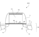
図1に本願発明を適用した不揮発性半導体メモリー100の断面図を示す。不揮発性半導体メモリー100は、シリコン基板12を用いて形成され、第1電極10、サイドウォール11、ソース領域/ドレイン領域13、シリサイド領域14、シリサイド層15、第1シリコン酸化膜20、第1シリコン窒化膜21、第2シリコン酸化膜22及び第2シリコン窒化膜23を有する。第1電極10としては、例えばポリシリコン膜、サイドウォール11としては、例えばシリコン酸化膜が用いられる。ソース領域/ドレイン領域13及びシリサイド領域14は、シリコン基板12内に形成された領域である。シリサイドは、例えばコバルトシリサイドやチタンシリサイドが用いられる。また、メモリー機能のためのトラップ層は、第1シリコン酸化膜20、第1シリコン窒化膜21及び第2シリコン酸化膜22から構成されるONO構造である。第2シリコン窒化膜23は、第1シリコン窒化膜21及びシリコン基板12に接している。以後、特に断りがない限り、シリコン基板12は、ソース領域/ドレイン領域13及びシリサイド領域14を含む意味で記載する。
(First embodiment)
FIG. 1 shows a cross-sectional view of a
比較のため、図9に、従来の不揮発性半導体メモリー900の断面図を示す。不揮発性半導体メモリー900は、第2シリコン窒化膜23が無い点で、本願発明を適用した不揮発性半導体メモリー100と異なる。不揮発性半導体メモリー900においては、サイドウォール11として、シリコン酸化膜が用いられるのが一般的であり、その場合、第1シリコン窒化膜の側面は、シリコン酸化膜に覆われる。
For comparison, FIG. 9 shows a cross-sectional view of a conventional
不揮発性半導体メモリー100及び900の製造過程においては、エッチングやスパッタリング等のプラズマを用いる処理を多用するが、その際に第1シリコン酸化膜20、第1シリコン窒化膜21及び第2シリコン酸化膜22から構成されるONO構造(トラップ層)にプラズマ由来の電荷が注入され、保持される。このような現象を本願ではプロセスチャージと呼ぶ。プロセスチャージが発生した場合、従来の不揮発性半導体メモリー900においては、シリコン酸化膜の絶縁性が高いために、プロセスチャージによる電荷を拡散させることが困難である。そのため、トラップ層に多くの電荷が捕獲されたまま製造工程が終了し、高速・低電圧動作に不向きな不揮発性半導体メモリーとなる場合がある。また、メモリーの閾値電圧が設計値から変動するため、閾値電圧の変動を伴うチャネル部の不純物濃度の変更・調整に制限がある。
In the manufacturing process of the
本願発明を適用した不揮発性半導体メモリー100(図1)においては、従来の不揮発性半導体メモリー900に対して、新たに第2シリコン窒化膜23を設けた。第2シリコン窒化膜23は、第1シリコン窒化膜21の側面と、シリコン基板12に接している。シリコン窒化膜は、シリコン酸化膜に比べて絶縁性が低い。そこで、トラップ層に保持されたプロセスチャージによる電荷を、第2シリコン窒化膜23を介してシリコン基板12に拡散させることが可能となる。電荷の拡散は、加熱処理を行うことで、加速される。加熱処理は、不純物の活性化やシリサイド化等、メモリーの製造過程で従来から行われる加熱処理を用いてもよいし、専用の工程を設けてもよい。第2シリコン窒化膜23は、シリコン酸化膜より絶縁性の低い絶縁膜であればよい。例えばシリコン酸窒化膜でもよい。
In the nonvolatile semiconductor memory 100 (FIG. 1) to which the present invention is applied, a second
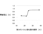
図5には、第2シリコン窒化膜の膜厚と、不揮発性半導体メモリー100及び900の閾値電圧の関係を表すグラフを示した。ここではプロセスチャージによって、電子がトラップ層に蓄積され、閾値電圧が上昇する。第2シリコン窒化膜が0Åすなわち不揮発性半導体メモリー900の場合、閾値電圧は1.0Vである。一方、第2シリコン窒化膜の膜厚が0Åより大きい不揮発性半導体メモリー100の場合、第2シリコン窒化膜の膜厚が大きくなるにつれて、トラップ層に蓄積された電子が拡散され、閾値電圧が低下する。第2シリコン窒化膜の膜厚が45Å以上の場合、閾値電圧が0.6V付近に低下して安定するようになるので、特に好ましい。この閾値電圧の膜厚依存性は、後述の第2〜第4実施形態でも同じである。
FIG. 5 shows a graph showing the relationship between the thickness of the second silicon nitride film and the threshold voltage of the
(第2実施形態)
本実施形態も含め、以降に記載する実施形態の説明において、第1実施形態と同様の構成要素については同じ番号を付与し、その説明を省略する。
(Second Embodiment)
In the description of the embodiments described below including this embodiment, the same numbers are assigned to the same components as those in the first embodiment, and the description thereof is omitted.
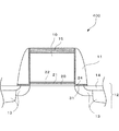
図2に本願発明を適用した不揮発性半導体メモリー200の断面図を示す。不揮発性半導体メモリー200は、不揮発性半導体メモリー100の構成要素に第3シリコン酸化膜30を付加したものである。第2シリコン窒化膜23は、第3シリコン酸化膜30を介してシリコン基板12に接している。第3シリコン酸化膜30の厚さは、第1シリコン酸化膜20の厚さよりも薄く形成されている。これにより、第1シリコン酸化膜20が第1シリコン窒化膜21の電荷を拡散することに対する障壁となっていても、第3シリコン酸化膜30を介して該電荷を拡散することができる。
FIG. 2 shows a cross-sectional view of a
図6には、第3シリコン酸化膜の膜厚と、不揮発性半導体メモリー200の閾値電圧の関係を表すグラフを示した。ここではプロセスチャージによって電子が、トラップ層に蓄積され、閾値電圧が上昇する。不揮発性半導体メモリー200においては、第3シリコン酸化膜の膜厚が小さくなるにつれて、トラップ層に蓄積された電子が拡散され、閾値電圧が低下する。第3シリコン酸化膜の膜厚が22Å以下の場合、閾値電圧が0.5V付近に低下して安定するようになるので、特に好ましい。この閾値電圧の膜厚依存性は、後述の第4実施形態でも同じである。
FIG. 6 shows a graph showing the relationship between the film thickness of the third silicon oxide film and the threshold voltage of the
尚、第3シリコン酸化膜30は、意図的に形成されるものでもよく、第2シリコン窒化膜23が形成される前の工程で自然発生的に形成されるものでもよい。
The third
(第3実施形態)
図3に本願発明を適用した不揮発性半導体メモリー300の断面図を示す。不揮発性半導体メモリー300は、シリコン基板12及び第1電極10に接する第2シリコン窒化膜24を有する。サイドウォール11は、第2シリコン窒化膜24を覆うように形成されている。上記した第2シリコン窒化膜23と同様に、第2シリコン窒化膜24の厚さは45Å以上であることが好ましい。
(Third embodiment)
FIG. 3 shows a cross-sectional view of a
第1シリコン窒化膜21に捕獲された電荷は、第2シリコン窒化膜24を介して第1電極10及びシリコン基板12に拡散されることになり、シリコン基板12のみに拡散させる場合よりも効率がよくなる。これにより、加熱処理の温度の設定及び時間の設定に対する自由度を上げることができる。
The charges trapped in the first
(第4実施形態)
図4に本願発明を適用した不揮発性半導体メモリー400の断面図を示す。不揮発性半導体メモリー400は、不揮発性半導体メモリー300の構成要素に第3シリコン酸化膜31を付加したものである。第2シリコン窒化膜24は、第3シリコン酸化膜31を介してシリコン基板12に接している。第3シリコン酸化膜31の厚さは、第1シリコン酸化膜20の厚さよりも薄く形成されている。これにより、第1シリコン酸化膜20が第1シリコン窒化膜21の電荷を拡散させることに対する障壁となっても、第3シリコン酸化膜31を介して該電荷を拡散させることができる。上記した第3シリコン酸化膜30と同様に、第3シリコン酸化膜31の厚さは22Å以下であることが好ましい。
(Fourth embodiment)
FIG. 4 shows a cross-sectional view of a
第3シリコン酸化膜31は、意図的に形成されるものでもよく、第2シリコン窒化膜24が形成される前の工程で自然発生的に形成されるものでもよい。
The third
上記した不揮発性半導体メモリー100、200、300及び400のいずれもシリコン基板12内にシリサイド領域14が形成されている。シリサイド領域14はシリコン基板12の他の部分に比較して電気抵抗が低いことから、シリサイド領域14を設けることがプロセスチャージの電荷を基板に拡散させる工程の効率を上げることに繋がり好ましい。
All of the
(第5実施形態)
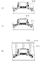
本実施形態は、本発明にかかるONO構造を有する不揮発性半導体メモリーの製造方法の1例を説明するものである。具体的には、上述した不揮発性半導体メモリー300若しくは400の製造方法となる。図7及び図8に、製造過程における素子の断面図の模式図を示す。尚、図に示しているのは、不揮発性半導体メモリーの部分のみであり、他の種類の素子の形成も同時に行われている。また、該不揮発性半導体メモリーを形成する領域をONO領域と呼ぶことにする。
(Fifth embodiment)
In the present embodiment, an example of a method for manufacturing a nonvolatile semiconductor memory having an ONO structure according to the present invention will be described. Specifically, the manufacturing method of the
図7−(a)は、シリコン基板501にSTI(Shallow Trench Isolation)502形成後に、ダミー酸化膜503を形成した状態を示す。ダミー酸化膜503は、ONO構造を形成するときのONO領域以外の領域に対するONO除去時の基板への影響を無くすためのものである。その後、ONO領域におけるダミー酸化膜503は除去され、ONO構造が積層される。図7−(b)は、ONO構造が積層された後、ダミー酸化膜503上に形成されたONO構造を除去した状態を示したものである。その後、残っていたダミー酸化膜503が除去され、ONO領域以外のトランジスターのゲート酸化膜が形成される。ONO領域におけるONO構造は、第1シリコン酸化膜504、第1シリコン窒化膜505及び第2シリコン酸化膜506から構成される。
FIG. 7A shows a state in which a
次に、ポリシリコンが全面に成膜され、ドライエッチングにより所定の形状の第1ゲート電極507が形成される(図7−(c))。該ドライエッチングの工程が、プロセスチャージが引き起こす工程となる(以下、電荷蓄積工程と称する)。その後、デバイスに応じたイオン注入が行われ不純物領域509が形成され、その後第2シリコン窒化膜508が成膜される(図7−(d))。
Next, polysilicon is formed on the entire surface, and a
次に、サイドウォールを形成するためにシリコン酸化膜を成膜し、異方性エッチングによりサイドウォール510が形成される。この異方性エッチングも電荷蓄積工程である。シリコン窒化膜はストレスの大きい膜なので、シリコン窒化膜のみでサイドウォールを形成すると、ストレスによる不具合が発生する場合がある。したがって、サイドウォール510をシリコン窒化膜だけでなく、シリコン酸化膜との積層構造とすることが好ましい。続いて、ソース領域/ドレイン領域を形成するためのイオンを注入し、活性化アニールが行われる。(図8−(e))。該活性化アニールは、プロセスチャージを拡散する工程となる(以下、電荷拡散工程と称する)。第1シリコン窒化膜505及び第2シリコン窒化膜508に蓄積された電荷が、該活性化アニールにより、シリコン基板501及び第1ゲート電極507に拡散する。
Next, a silicon oxide film is formed to form sidewalls, and sidewalls 510 are formed by anisotropic etching. This anisotropic etching is also a charge accumulation process. Since the silicon nitride film is a highly stressed film, if a sidewall is formed only with the silicon nitride film, a problem due to stress may occur. Therefore, it is preferable that the
次に、Co(コバルト)をスパッタリングしアニールすることで、コバルトシリサイド領域511およびコバルトシリサイド層515が形成される。この工程においては、該スパッタリングが電荷蓄積工程となり、該アニールが電荷拡散工程となる。(図8−(f))。
Next, Co (cobalt) is sputtered and annealed to form a
次に、層間絶縁膜512を形成し、ドライエッチングによりコンタクトホール513を形成する。該ドライエッチングが電荷蓄積工程となるが、この後のタングステン等を成膜しアニールし配線514を形成する工程が電荷拡散工程となる(図8−(g)。
Next, an
以降、必要な層数の層間絶縁膜の形成、コンタクトホールの形成及び配線の形成を行うために、所定のスパッタリング、所定のエッチング及び所定のアニールが行われ、電荷蓄積工程と電荷拡散工程が繰り返される。電荷蓄積工程で第1シリコン酸化膜504、第1シリコン窒化膜505及び第2シリコン酸化膜506から構成されるONO構造(トラップ層)に蓄積された電荷が、電荷拡散工程でシリコン基板501及び第1ゲート電極507に拡散させることができる。製造に必要な工程のすべてが終了する時点で、トラップ層に電荷が捕獲されたままにならないようにするには、最終の電荷蓄積工程より後に、電荷拡散工程を設けることが好ましい。最終工程が電荷拡散工程であることがさらに好ましい。これにより、プロセスチャージによる弊害をなくした不揮発性半導体メモリーを製造することが可能となる。
Thereafter, in order to form the required number of interlayer insulating films, contact holes and wirings, predetermined sputtering, predetermined etching and predetermined annealing are performed, and the charge accumulation process and the charge diffusion process are repeated. It is. The charges accumulated in the ONO structure (trap layer) composed of the first
また、上記の製造工程において、第2シリコン窒化膜508が成膜される前に第3シリコン酸化膜を形成する工程を付加してもよい。例えば、ドライエッチングにより所定の形状の第1ゲート電極507が形成される際に、前記シリコン基板を露出させない様にシリコン酸化膜を残すように加工する事で、第3シリコン酸化膜を意図的に形成してもよい。尚或いは、製造過程の中でシリコン基板と第2シリコン窒化膜との間に自然発生的に形成されるシリコン酸化膜を、第3シリコン酸化膜として利用することを考慮して製造工程を構成してもよい。
In the above manufacturing process, a step of forming a third silicon oxide film may be added before the second
本実施形態として、不揮発性半導体メモリー300若しくは400の場合の製造方法の説明を行ったが、不揮発性半導体メモリー100若しくは200の場合は第2シリコン窒化膜の形状が異なることから製造工程が異なってくる。しかしながら、電荷蓄積工程の後に電荷拡散工程が存在するようにすることで、本実施形態で説明した製造方法における効果と同様の効果を得ることができる。
In the present embodiment, the manufacturing method in the case of the
以上、本発明にかかる適用例及び実施形態について記載したが、本発明は上述した記載に限定されるものではない。本発明は、趣旨を逸脱しない範囲において広く適用が可能である。 As mentioned above, although the application example and embodiment concerning this invention were described, this invention is not limited to the description mentioned above. The present invention can be widely applied without departing from the spirit of the present invention.
10…第1電極、11…サイドウォール、12…シリコン基板、13…ソース/ドレイン領域、14…シリサイド領域、15…シリサイド層、20…第1シリコン酸化膜、21…第1シリコン窒化膜、22…第2シリコン酸化膜、23…第2シリコン窒化膜、24…第2シリコン窒化膜、30…第3シリコン酸化膜、31…第3シリコン酸化膜、100…不揮発性半導体メモリー、200…不揮発性半導体メモリー、300…不揮発性半導体メモリー、400…不揮発性半導体メモリー、501…シリコン基板、502…STI、503…ダミー酸化膜、504…第1シリコン酸化膜、505…第1シリコン窒化膜、506…第2シリコン酸化膜、507…第1ゲート電極、508…第2シリコン窒化膜、509…不純物領域、510…サイドウォール、511…コバルトシリサイド領域、512…層間絶縁膜、513…コンタクトホール、514…配線、515…コバルトシリサイド層、900…不揮発性半導体メモリー。
DESCRIPTION OF
Claims (6)
シリコン基板と、
第1のシリコン酸化膜と、
第2のシリコン酸化膜と、
第3のシリコン酸化膜と、
第1のシリコン窒化膜と、
第2のシリコン窒化膜と、を含み、
前記第1のシリコン酸化膜および前記第3のシリコン酸化膜は、前記シリコン基板上に積層され、
前記第1のシリコン窒化膜は、前記第1のシリコン酸化膜上に積層され、
前記第2のシリコン酸化膜は、前記第1のシリコン窒化膜上に積層され、
前記第3のシリコン酸化膜の厚さは、前記第1のシリコン酸化膜の厚さよりも薄く、
前記第2のシリコン窒化膜は、第1の部分が前記第1のシリコン窒化膜に接すると共に第2の部分が前記第3のシリコン酸化膜に接しており、
前記第3のシリコン酸化膜は、厚さが0Åより大きく22Å以下であることを特徴とする不揮発性半導体メモリー。 Non-volatile semiconductor memory,
A silicon substrate;
A first silicon oxide film;
A second silicon oxide film;
A third silicon oxide film;
A first silicon nitride film;
A second silicon nitride film,
The first silicon oxide film and the third silicon oxide film are stacked on the silicon substrate,
The first silicon nitride film is stacked on the first silicon oxide film,
The second silicon oxide film is stacked on the first silicon nitride film,
The thickness of the third silicon oxide film is thinner than the thickness of the first silicon oxide film,
The second silicon nitride film has a first portion in contact with the first silicon nitride film and a second portion in contact with the third silicon oxide film ,
The non-volatile semiconductor memory according to claim 3, wherein the third silicon oxide film has a thickness of more than 0 mm and not more than 22 mm .
前記シリサイド領域は、前記第3のシリコン酸化膜に接することを特徴する請求項1に記載の不揮発性半導体メモリー。 Furthermore, a silicide region is included in the silicon substrate,
The nonvolatile semiconductor memory according to claim 1, wherein the silicide region is in contact with the third silicon oxide film.
前記第2のシリコン窒化膜の第3の部分が前記第1の電極に接していることを特徴とする請求項1又は2に記載の不揮発性半導体メモリー。 And a first electrode on the second silicon oxide film,
The nonvolatile semiconductor memory according to claim 1, wherein a third portion of the second silicon nitride film is in contact with the first electrode.
シリコン基板上に、第1のシリコン酸化膜を成膜する第1の工程と、
前記第1のシリコン酸化膜上に、第1のシリコン窒化膜を成膜する第2の工程と、
前記第1のシリコン窒化膜上に、第2のシリコン酸化膜を成膜する第3の工程と、
前記第1のシリコン酸化膜、前記第1のシリコン窒化膜及び第2のシリコン酸化膜を所定の形状にパターニングする第4の工程と、
前記第4の工程の後に第2のシリコン窒化膜を成膜する第5の工程と、を含み、
前記第4の工程において、前記第1のシリコン窒化膜及び前記シリコン基板が露出され、
前記第4の工程と前記第5の工程の間の第6の工程において、前記シリコン基板が露出された領域に前記第1のシリコン酸化膜より膜厚が薄い第3のシリコン酸化膜が形成され、
前記第3のシリコン酸化膜は、厚さが0Åより大きく22Å以下であり、
前記第5の工程において、前記第1のシリコン窒化膜と前記第2のシリコン窒化膜とが接することを特徴とする不揮発性半導体メモリーの製造方法。 A method for manufacturing a nonvolatile semiconductor memory, comprising:
A first step of forming a first silicon oxide film on a silicon substrate;
A second step of forming a first silicon nitride film on the first silicon oxide film;
A third step of forming a second silicon oxide film on the first silicon nitride film;
A fourth step of patterning the first silicon oxide film, the first silicon nitride film, and the second silicon oxide film into a predetermined shape;
And a fifth step of forming a second silicon nitride film after the fourth step,
In the fourth step, the first silicon nitride film and the silicon substrate are exposed,
In a sixth step between the fourth step and the fifth step, a third silicon oxide film having a thickness smaller than that of the first silicon oxide film is formed in a region where the silicon substrate is exposed. ,
The third silicon oxide film has a thickness greater than 0 mm and not greater than 22 mm;
The method of manufacturing a nonvolatile semiconductor memory, wherein the first silicon nitride film and the second silicon nitride film are in contact with each other in the fifth step.
シリコン基板上に、第1のシリコン酸化膜を成膜する第1の工程と、
前記第1のシリコン酸化膜上に、第1のシリコン窒化膜を成膜する第2の工程と、
前記第1のシリコン窒化膜上に、第2のシリコン酸化膜を成膜する第3の工程と、
前記第1のシリコン酸化膜、前記第1のシリコン窒化膜及び第2のシリコン酸化膜を所定の形状にパターニングする第4の工程と、
前記第4の工程の後に第2のシリコン窒化膜を成膜する第5の工程と、を含み、
前記第4の工程において、前記第1のシリコン窒化膜が露出され、前記第1のシリコン酸化膜をエッチングすることで前記第1のシリコン酸化膜より膜厚が薄い第3のシリコン酸化膜が形成され、
前記第3のシリコン酸化膜は、厚さが0Åより大きく22Å以下であり、
前記第5の工程において、前記第1のシリコン窒化膜と前記第2のシリコン窒化膜とが接することを特徴とする不揮発性半導体メモリーの製造方法。 A method for manufacturing a nonvolatile semiconductor memory, comprising:
A first step of forming a first silicon oxide film on a silicon substrate;
A second step of forming a first silicon nitride film on the first silicon oxide film;
A third step of forming a second silicon oxide film on the first silicon nitride film;
A fourth step of patterning the first silicon oxide film, the first silicon nitride film, and the second silicon oxide film into a predetermined shape;
And a fifth step of forming a second silicon nitride film after the fourth step,
In the fourth step, the first silicon nitride film is exposed, and a third silicon oxide film having a thickness smaller than that of the first silicon oxide film is formed by etching the first silicon oxide film. And
The third silicon oxide film has a thickness greater than 0 mm and not greater than 22 mm;
The method of manufacturing a nonvolatile semiconductor memory, wherein the first silicon nitride film and the second silicon nitride film are in contact with each other in the fifth step.
Priority Applications (6)
| Application Number | Priority Date | Filing Date | Title |
|---|---|---|---|
| JP2012041221A JP5998521B2 (en) | 2012-02-28 | 2012-02-28 | Nonvolatile semiconductor memory and method for manufacturing nonvolatile semiconductor memory |
| PCT/JP2013/001031 WO2013128864A1 (en) | 2012-02-28 | 2013-02-22 | Non-volatile semiconductor memory, and production method for non-volatile semiconductor memory |
| CN201380010880.4A CN104137239B (en) | 2012-02-28 | 2013-02-22 | The manufacture method of nonvolatile semiconductor memory and nonvolatile semiconductor memory |
| KR1020147026353A KR101618160B1 (en) | 2012-02-28 | 2013-02-22 | Non-volatile semiconductor memory, and production method for non-volatile semiconductor memory |
| US14/377,278 US9461138B2 (en) | 2012-02-28 | 2013-02-22 | Non-volatile semiconductor memory with nitride sidewall contacting nitride layer of ONO gate stack and methods for producing the same |
| TW102106457A TWI609480B (en) | 2012-02-28 | 2013-02-23 | Non-volatile semiconductor memory and non-volatile semiconductor memory manufacturing method |
Applications Claiming Priority (1)
| Application Number | Priority Date | Filing Date | Title |
|---|---|---|---|
| JP2012041221A JP5998521B2 (en) | 2012-02-28 | 2012-02-28 | Nonvolatile semiconductor memory and method for manufacturing nonvolatile semiconductor memory |
Publications (3)
| Publication Number | Publication Date |
|---|---|
| JP2013179122A JP2013179122A (en) | 2013-09-09 |
| JP2013179122A5 JP2013179122A5 (en) | 2015-04-02 |
| JP5998521B2 true JP5998521B2 (en) | 2016-09-28 |
Family
ID=49082077
Family Applications (1)
| Application Number | Title | Priority Date | Filing Date |
|---|---|---|---|
| JP2012041221A Active JP5998521B2 (en) | 2012-02-28 | 2012-02-28 | Nonvolatile semiconductor memory and method for manufacturing nonvolatile semiconductor memory |
Country Status (6)
| Country | Link |
|---|---|
| US (1) | US9461138B2 (en) |
| JP (1) | JP5998521B2 (en) |
| KR (1) | KR101618160B1 (en) |
| CN (1) | CN104137239B (en) |
| TW (1) | TWI609480B (en) |
| WO (1) | WO2013128864A1 (en) |
Families Citing this family (20)
| Publication number | Priority date | Publication date | Assignee | Title |
|---|---|---|---|---|
| JP6880595B2 (en) | 2016-08-10 | 2021-06-02 | セイコーエプソン株式会社 | Semiconductor devices and their manufacturing methods |
| US10777566B2 (en) | 2017-11-10 | 2020-09-15 | Macronix International Co., Ltd. | 3D array arranged for memory and in-memory sum-of-products operations |
| US10719296B2 (en) | 2018-01-17 | 2020-07-21 | Macronix International Co., Ltd. | Sum-of-products accelerator array |
| US20190244662A1 (en) * | 2018-02-02 | 2019-08-08 | Macronix International Co., Ltd. | Sum-of-products array for neuromorphic computing system |
| US10957392B2 (en) | 2018-01-17 | 2021-03-23 | Macronix International Co., Ltd. | 2D and 3D sum-of-products array for neuromorphic computing system |
| JP6976190B2 (en) * | 2018-02-20 | 2021-12-08 | キオクシア株式会社 | Storage device |
| US10635398B2 (en) | 2018-03-15 | 2020-04-28 | Macronix International Co., Ltd. | Voltage sensing type of matrix multiplication method for neuromorphic computing system |
| US11138497B2 (en) | 2018-07-17 | 2021-10-05 | Macronix International Co., Ltd | In-memory computing devices for neural networks |
| US11636325B2 (en) | 2018-10-24 | 2023-04-25 | Macronix International Co., Ltd. | In-memory data pooling for machine learning |
| US10672469B1 (en) | 2018-11-30 | 2020-06-02 | Macronix International Co., Ltd. | In-memory convolution for machine learning |
| US11562229B2 (en) | 2018-11-30 | 2023-01-24 | Macronix International Co., Ltd. | Convolution accelerator using in-memory computation |
| US11934480B2 (en) | 2018-12-18 | 2024-03-19 | Macronix International Co., Ltd. | NAND block architecture for in-memory multiply-and-accumulate operations |
| US11119674B2 (en) | 2019-02-19 | 2021-09-14 | Macronix International Co., Ltd. | Memory devices and methods for operating the same |
| US10783963B1 (en) | 2019-03-08 | 2020-09-22 | Macronix International Co., Ltd. | In-memory computation device with inter-page and intra-page data circuits |
| US11132176B2 (en) | 2019-03-20 | 2021-09-28 | Macronix International Co., Ltd. | Non-volatile computing method in flash memory |
| US10910393B2 (en) | 2019-04-25 | 2021-02-02 | Macronix International Co., Ltd. | 3D NOR memory having vertical source and drain structures |
| JP2021061450A (en) * | 2021-01-20 | 2021-04-15 | セイコーエプソン株式会社 | Semiconductor device and method of manufacturing the same |
| US11737274B2 (en) | 2021-02-08 | 2023-08-22 | Macronix International Co., Ltd. | Curved channel 3D memory device |
| US11916011B2 (en) | 2021-04-14 | 2024-02-27 | Macronix International Co., Ltd. | 3D virtual ground memory and manufacturing methods for same |
| US11710519B2 (en) | 2021-07-06 | 2023-07-25 | Macronix International Co., Ltd. | High density memory with reference memory using grouped cells and corresponding operations |
Family Cites Families (23)
| Publication number | Priority date | Publication date | Assignee | Title |
|---|---|---|---|---|
| JPH07226502A (en) | 1994-02-14 | 1995-08-22 | Sony Corp | Mos transistor and manufacture thereof |
| JP3240999B2 (en) | 1998-08-04 | 2001-12-25 | 日本電気株式会社 | Semiconductor memory device and method of manufacturing the same |
| JP3482171B2 (en) | 1999-03-25 | 2003-12-22 | 松下電器産業株式会社 | Semiconductor device and manufacturing method thereof |
| US6573132B1 (en) | 1999-03-25 | 2003-06-03 | Matsushita Electric Industrial Co., Ltd. | Method for fabricating a semiconductor device having contacts self-aligned with a gate electrode thereof |
| JP4730999B2 (en) * | 2000-03-10 | 2011-07-20 | スパンション エルエルシー | Method for manufacturing nonvolatile memory |
| JP3961211B2 (en) | 2000-10-31 | 2007-08-22 | 株式会社東芝 | Manufacturing method of semiconductor device |
| JP2002222876A (en) | 2001-01-25 | 2002-08-09 | Sony Corp | Non-volatile semiconductor memory device and method of manufacturing the same |
| JP3641596B2 (en) | 2001-05-09 | 2005-04-20 | 株式会社東芝 | Semiconductor memory device and manufacturing method thereof |
| US6555865B2 (en) | 2001-07-10 | 2003-04-29 | Samsung Electronics Co. Ltd. | Nonvolatile semiconductor memory device with a multi-layer sidewall spacer structure and method for manufacturing the same |
| JP2003264247A (en) * | 2002-03-11 | 2003-09-19 | Toshiba Corp | Nonvolatile semiconductor memory and its manufacturing method |
| JP3987418B2 (en) | 2002-11-15 | 2007-10-10 | 株式会社東芝 | Semiconductor memory device |
| KR100463184B1 (en) | 2003-01-30 | 2004-12-23 | 아남반도체 주식회사 | Fabrication method of Non-volatile memory device |
| KR100546692B1 (en) * | 2004-05-03 | 2006-01-26 | 동부아남반도체 주식회사 | Method for fabricating of flash memory device |
| JP2006032541A (en) | 2004-07-14 | 2006-02-02 | Renesas Technology Corp | Semiconductor device |
| KR100642898B1 (en) | 2004-07-21 | 2006-11-03 | 에스티마이크로일렉트로닉스 엔.브이. | Transistor of semiconductor device and mathod for manufacturing the same |
| WO2006080081A1 (en) * | 2005-01-28 | 2006-08-03 | Spansion Llc | Non-volatile memory and control method thereof |
| US7405441B2 (en) * | 2005-03-11 | 2008-07-29 | Infineon Technology Ag | Semiconductor memory |
| JP4783044B2 (en) * | 2005-03-23 | 2011-09-28 | 株式会社Genusion | Nonvolatile semiconductor memory device |
| JP2007005699A (en) * | 2005-06-27 | 2007-01-11 | Matsushita Electric Ind Co Ltd | Nonvolatile semiconductor storage device and its manufacturing method |
| JP2008218727A (en) | 2007-03-05 | 2008-09-18 | Renesas Technology Corp | Semiconductor device and manufacturing method thereof |
| JP2009071325A (en) * | 2008-11-25 | 2009-04-02 | Renesas Technology Corp | Semiconductor device and method for manufacturing the same |
| US8471328B2 (en) * | 2010-07-26 | 2013-06-25 | United Microelectronics Corp. | Non-volatile memory and manufacturing method thereof |
| US8629025B2 (en) * | 2012-02-23 | 2014-01-14 | United Microelectronics Corp. | Semiconductor device and method for fabricating semiconductor device |
-
2012
- 2012-02-28 JP JP2012041221A patent/JP5998521B2/en active Active
-
2013
- 2013-02-22 US US14/377,278 patent/US9461138B2/en active Active
- 2013-02-22 KR KR1020147026353A patent/KR101618160B1/en active IP Right Grant
- 2013-02-22 CN CN201380010880.4A patent/CN104137239B/en active Active
- 2013-02-22 WO PCT/JP2013/001031 patent/WO2013128864A1/en active Application Filing
- 2013-02-23 TW TW102106457A patent/TWI609480B/en active
Also Published As
| Publication number | Publication date |
|---|---|
| JP2013179122A (en) | 2013-09-09 |
| KR20140136000A (en) | 2014-11-27 |
| US20150008500A1 (en) | 2015-01-08 |
| TW201347149A (en) | 2013-11-16 |
| CN104137239A (en) | 2014-11-05 |
| TWI609480B (en) | 2017-12-21 |
| WO2013128864A1 (en) | 2013-09-06 |
| US9461138B2 (en) | 2016-10-04 |
| KR101618160B1 (en) | 2016-05-04 |
| CN104137239B (en) | 2018-01-12 |
Similar Documents
| Publication | Publication Date | Title |
|---|---|---|
| JP5998521B2 (en) | Nonvolatile semiconductor memory and method for manufacturing nonvolatile semiconductor memory | |
| JP4885420B2 (en) | Source / drain implantation during ONO formation to improve isolation of SONOS type devices | |
| JP2012114269A (en) | Semiconductor device and method of manufacturing semiconductor device | |
| JP4357526B2 (en) | Nonvolatile semiconductor memory device and manufacturing method thereof | |
| JP5538828B2 (en) | Semiconductor device and manufacturing method thereof | |
| TW201030945A (en) | Nonvolatile memory cell and method for fabricating the same | |
| US20100270604A1 (en) | Non-Volatile Memories and Methods of Fabrication Thereof | |
| JP2010087046A (en) | Nonvolatile semiconductor device and method of manufacturing the same | |
| JP4783595B2 (en) | Semiconductor device DRAM manufacturing method | |
| KR100606928B1 (en) | Non-volatile memory device and fabricating method for the same | |
| TWI228834B (en) | Method of forming a non-volatile memory device | |
| TWI555131B (en) | Nor flash memory and manufacturing method thereof | |
| CN106206748B (en) | SONOS device and manufacturing method thereof | |
| JP2016051740A (en) | Method of manufacturing semiconductor device | |
| KR100806039B1 (en) | Flash memory device and method for manufacturing the flash memory device | |
| JP5937172B2 (en) | Semiconductor device and manufacturing method of semiconductor device | |
| JP5421549B2 (en) | Semiconductor device manufacturing method and semiconductor device | |
| CN110729301A (en) | Semiconductor device and method for manufacturing the same | |
| JP2005197684A (en) | Semiconductor device | |
| US20090218615A1 (en) | Semiconductor device and method of manufacturing the same | |
| JP5363004B2 (en) | Manufacturing method of semiconductor device | |
| JPH1167940A (en) | Nonvolatile semiconductor storage device and manufacture thereof | |
| KR100668727B1 (en) | Method for Fabricating of Flash Memory Device | |
| KR20100025717A (en) | Manufacturing method of semiconductor device | |
| JP2010129594A (en) | Semiconductor memory device, and method of manufacturing the same |
Legal Events
| Date | Code | Title | Description |
|---|---|---|---|
| RD04 | Notification of resignation of power of attorney |
Free format text: JAPANESE INTERMEDIATE CODE: A7424 Effective date: 20150107 |
|
| A521 | Request for written amendment filed |
Free format text: JAPANESE INTERMEDIATE CODE: A523 Effective date: 20150213 |
|
| A621 | Written request for application examination |
Free format text: JAPANESE INTERMEDIATE CODE: A621 Effective date: 20150213 |
|
| A131 | Notification of reasons for refusal |
Free format text: JAPANESE INTERMEDIATE CODE: A131 Effective date: 20150818 |
|
| A521 | Request for written amendment filed |
Free format text: JAPANESE INTERMEDIATE CODE: A523 Effective date: 20151016 |
|
| A131 | Notification of reasons for refusal |
Free format text: JAPANESE INTERMEDIATE CODE: A131 Effective date: 20160524 |
|
| RD04 | Notification of resignation of power of attorney |
Free format text: JAPANESE INTERMEDIATE CODE: A7424 Effective date: 20160609 |
|
| RD03 | Notification of appointment of power of attorney |
Free format text: JAPANESE INTERMEDIATE CODE: A7423 Effective date: 20160613 |
|
| A521 | Request for written amendment filed |
Free format text: JAPANESE INTERMEDIATE CODE: A523 Effective date: 20160708 |
|
| TRDD | Decision of grant or rejection written | ||
| A01 | Written decision to grant a patent or to grant a registration (utility model) |
Free format text: JAPANESE INTERMEDIATE CODE: A01 Effective date: 20160802 |
|
| A61 | First payment of annual fees (during grant procedure) |
Free format text: JAPANESE INTERMEDIATE CODE: A61 Effective date: 20160815 |
|
| R150 | Certificate of patent or registration of utility model |
Ref document number: 5998521 Country of ref document: JP Free format text: JAPANESE INTERMEDIATE CODE: R150 |