JP5981154B2 - 半導体装置の製造方法 - Google Patents
半導体装置の製造方法 Download PDFInfo
- Publication number
- JP5981154B2 JP5981154B2 JP2012020829A JP2012020829A JP5981154B2 JP 5981154 B2 JP5981154 B2 JP 5981154B2 JP 2012020829 A JP2012020829 A JP 2012020829A JP 2012020829 A JP2012020829 A JP 2012020829A JP 5981154 B2 JP5981154 B2 JP 5981154B2
- Authority
- JP
- Japan
- Prior art keywords
- support member
- thin
- thick
- semiconductor device
- semiconductor wafer
- Prior art date
- Legal status (The legal status is an assumption and is not a legal conclusion. Google has not performed a legal analysis and makes no representation as to the accuracy of the status listed.)
- Active
Links
Images


Classifications
-
- H—ELECTRICITY
- H01—ELECTRIC ELEMENTS
- H01L—SEMICONDUCTOR DEVICES NOT COVERED BY CLASS H10
- H01L21/00—Processes or apparatus adapted for the manufacture or treatment of semiconductor or solid state devices or of parts thereof
- H01L21/02—Manufacture or treatment of semiconductor devices or of parts thereof
- H01L21/04—Manufacture or treatment of semiconductor devices or of parts thereof the devices having at least one potential-jump barrier or surface barrier, e.g. PN junction, depletion layer or carrier concentration layer
- H01L21/18—Manufacture or treatment of semiconductor devices or of parts thereof the devices having at least one potential-jump barrier or surface barrier, e.g. PN junction, depletion layer or carrier concentration layer the devices having semiconductor bodies comprising elements of Group IV of the Periodic System or AIIIBV compounds with or without impurities, e.g. doping materials
- H01L21/30—Treatment of semiconductor bodies using processes or apparatus not provided for in groups H01L21/20 - H01L21/26
-
- H—ELECTRICITY
- H01—ELECTRIC ELEMENTS
- H01L—SEMICONDUCTOR DEVICES NOT COVERED BY CLASS H10
- H01L21/00—Processes or apparatus adapted for the manufacture or treatment of semiconductor or solid state devices or of parts thereof
- H01L21/02—Manufacture or treatment of semiconductor devices or of parts thereof
- H01L21/02002—Preparing wafers
- H01L21/02005—Preparing bulk and homogeneous wafers
-
- H—ELECTRICITY
- H01—ELECTRIC ELEMENTS
- H01L—SEMICONDUCTOR DEVICES NOT COVERED BY CLASS H10
- H01L21/00—Processes or apparatus adapted for the manufacture or treatment of semiconductor or solid state devices or of parts thereof
- H01L21/02—Manufacture or treatment of semiconductor devices or of parts thereof
- H01L21/04—Manufacture or treatment of semiconductor devices or of parts thereof the devices having at least one potential-jump barrier or surface barrier, e.g. PN junction, depletion layer or carrier concentration layer
- H01L21/18—Manufacture or treatment of semiconductor devices or of parts thereof the devices having at least one potential-jump barrier or surface barrier, e.g. PN junction, depletion layer or carrier concentration layer the devices having semiconductor bodies comprising elements of Group IV of the Periodic System or AIIIBV compounds with or without impurities, e.g. doping materials
- H01L21/30—Treatment of semiconductor bodies using processes or apparatus not provided for in groups H01L21/20 - H01L21/26
- H01L21/302—Treatment of semiconductor bodies using processes or apparatus not provided for in groups H01L21/20 - H01L21/26 to change their surface-physical characteristics or shape, e.g. etching, polishing, cutting
- H01L21/304—Mechanical treatment, e.g. grinding, polishing, cutting
-
- H—ELECTRICITY
- H01—ELECTRIC ELEMENTS
- H01L—SEMICONDUCTOR DEVICES NOT COVERED BY CLASS H10
- H01L21/00—Processes or apparatus adapted for the manufacture or treatment of semiconductor or solid state devices or of parts thereof
- H01L21/67—Apparatus specially adapted for handling semiconductor or electric solid state devices during manufacture or treatment thereof; Apparatus specially adapted for handling wafers during manufacture or treatment of semiconductor or electric solid state devices or components ; Apparatus not specifically provided for elsewhere
- H01L21/683—Apparatus specially adapted for handling semiconductor or electric solid state devices during manufacture or treatment thereof; Apparatus specially adapted for handling wafers during manufacture or treatment of semiconductor or electric solid state devices or components ; Apparatus not specifically provided for elsewhere for supporting or gripping
- H01L21/6835—Apparatus specially adapted for handling semiconductor or electric solid state devices during manufacture or treatment thereof; Apparatus specially adapted for handling wafers during manufacture or treatment of semiconductor or electric solid state devices or components ; Apparatus not specifically provided for elsewhere for supporting or gripping using temporarily an auxiliary support
- H01L21/6836—Wafer tapes, e.g. grinding or dicing support tapes
-
- H—ELECTRICITY
- H01—ELECTRIC ELEMENTS
- H01L—SEMICONDUCTOR DEVICES NOT COVERED BY CLASS H10
- H01L21/00—Processes or apparatus adapted for the manufacture or treatment of semiconductor or solid state devices or of parts thereof
- H01L21/70—Manufacture or treatment of devices consisting of a plurality of solid state components formed in or on a common substrate or of parts thereof; Manufacture of integrated circuit devices or of parts thereof
- H01L21/77—Manufacture or treatment of devices consisting of a plurality of solid state components or integrated circuits formed in, or on, a common substrate
- H01L21/78—Manufacture or treatment of devices consisting of a plurality of solid state components or integrated circuits formed in, or on, a common substrate with subsequent division of the substrate into plural individual devices
-
- H—ELECTRICITY
- H01—ELECTRIC ELEMENTS
- H01L—SEMICONDUCTOR DEVICES NOT COVERED BY CLASS H10
- H01L2221/00—Processes or apparatus adapted for the manufacture or treatment of semiconductor or solid state devices or of parts thereof covered by H01L21/00
- H01L2221/67—Apparatus for handling semiconductor or electric solid state devices during manufacture or treatment thereof; Apparatus for handling wafers during manufacture or treatment of semiconductor or electric solid state devices or components; Apparatus not specifically provided for elsewhere
- H01L2221/683—Apparatus for handling semiconductor or electric solid state devices during manufacture or treatment thereof; Apparatus for handling wafers during manufacture or treatment of semiconductor or electric solid state devices or components; Apparatus not specifically provided for elsewhere for supporting or gripping
- H01L2221/68304—Apparatus for handling semiconductor or electric solid state devices during manufacture or treatment thereof; Apparatus for handling wafers during manufacture or treatment of semiconductor or electric solid state devices or components; Apparatus not specifically provided for elsewhere for supporting or gripping using temporarily an auxiliary support
- H01L2221/68327—Apparatus for handling semiconductor or electric solid state devices during manufacture or treatment thereof; Apparatus for handling wafers during manufacture or treatment of semiconductor or electric solid state devices or components; Apparatus not specifically provided for elsewhere for supporting or gripping using temporarily an auxiliary support used during dicing or grinding
- H01L2221/68331—Apparatus for handling semiconductor or electric solid state devices during manufacture or treatment thereof; Apparatus for handling wafers during manufacture or treatment of semiconductor or electric solid state devices or components; Apparatus not specifically provided for elsewhere for supporting or gripping using temporarily an auxiliary support used during dicing or grinding of passive members, e.g. die mounting substrate
Description
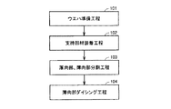
はじめに、図1を参照して、本実施の形態における半導体装置の製造方法の概略フローを説明する。まず、ステップ101にて、厚肉部と、半導体素子や配線が形成された薄肉部とを有する半導体ウエハを準備する。次に、ステップ102にて、支持部材を半導体ウエハの主表面と反対側に位置する裏面に装着する。その後、ステップ103にて、支持部材にて支持された状態で半導体ウエハを厚肉部と薄肉部とに分割する。分割後、ステップ104にて、半導体素子や配線が形成された薄肉部を、支持部材に支持された状態で個々の半導体装置に個片化する。
次に、図13と図14とを参照して、本発明の実施の形態2について説明する。本実施の形態の半導体装置の製造方法は、基本的に実施の形態1と同様の構成を備えているが、厚肉部1aを支持部材2から分離する工程の前に、厚肉部1aと接する部分における支持部材2の粘着力を低下させる工程を備える点で異なっている。
次に、本発明の実施の形態3について説明する。本実施の形態の半導体装置の製造方法は、基本的に実施の形態1と同様の構成を備えているが、薄肉部のダイシング工程をレーザダイシングにより実施する点で異なっている。
Claims (7)
- 外周端部に厚肉部を、中央部に薄肉部を有する半導体ウエハを準備する工程と、
前記半導体ウエハの一方の面に支持部材を装着する工程と、
前記支持部材の装着後に、前記半導体ウエハを前記厚肉部と前記薄肉部とに分割する工程と、
前記厚肉部を前記支持部材から分離した後に、前記支持部材を伸張させる工程と、
前記伸張させる工程の後に、前記支持部材で前記薄肉部を支持した状態で前記薄肉部を切断する工程と、を備え、
前記支持部材は、熱収縮性を有する粘着テープを含み、
前記装着する工程では、前記支持部材によって前記半導体ウエハがフレームにマウントされ、
前記分割する工程では、前記支持部材において前記薄肉部と接続されている部分が前記支持部材において前記フレームと接続されている部分よりも前記半導体ウエハの厚み方向において上方に位置している状態で実施され、
前記伸張させる工程は前記支持部材を加温する工程を含み、
前記加温する工程では、前記支持部材を介して前記薄肉部を保持する薄肉保持部が前記支持部材を介して前記フレームを保持するフレーム保持部よりも前記厚み方向において上方に位置している状態から、前記薄肉保持部と前記フレーム保持部とが同一平面上に位置するように移動させながら前記支持部材を加温する、半導体装置の製造方法。 - 前記分割後に前記厚肉部を前記支持部材から分離する工程をさらに備える、請求項1に記載の半導体装置の製造方法。
- 前記粘着テープは、前記薄肉部から前記厚肉部にわたって貼付られる、請求項1または請求項2に記載の半導体装置の製造方法。
- 前記厚肉部を、前記粘着テープから分離する前に、前記厚肉部と接する部分における前記粘着テープの粘着力を低下させる工程を備える、請求項3に記載の半導体装置の製造方法。
- 前記厚肉部を直接保持して分離する、請求項2〜請求項4のいずれか1項に記載の半導体装置の製造方法。
- 前記厚肉部を真空吸着することにより保持する、請求項5に記載の半導体装置の製造方法。
- 前記厚肉部を静電吸着することにより保持する、請求項5に記載の半導体装置の製造方法。
Priority Applications (5)
| Application Number | Priority Date | Filing Date | Title |
|---|---|---|---|
| JP2012020829A JP5981154B2 (ja) | 2012-02-02 | 2012-02-02 | 半導体装置の製造方法 |
| US13/708,358 US8993413B2 (en) | 2012-02-02 | 2012-12-07 | Method of manufacturing semiconductor device |
| DE102012223093.9A DE102012223093B4 (de) | 2012-02-02 | 2012-12-13 | Verfahren zur Herstellung einer Halbleitervorrichtung |
| KR1020130008382A KR101440393B1 (ko) | 2012-02-02 | 2013-01-25 | 반도체장치의 제조방법 |
| CN201310040271.5A CN103295892B (zh) | 2012-02-02 | 2013-02-01 | 半导体装置的制造方法 |
Applications Claiming Priority (1)
| Application Number | Priority Date | Filing Date | Title |
|---|---|---|---|
| JP2012020829A JP5981154B2 (ja) | 2012-02-02 | 2012-02-02 | 半導体装置の製造方法 |
Publications (3)
| Publication Number | Publication Date |
|---|---|
| JP2013161863A JP2013161863A (ja) | 2013-08-19 |
| JP2013161863A5 JP2013161863A5 (ja) | 2014-07-17 |
| JP5981154B2 true JP5981154B2 (ja) | 2016-08-31 |
Family
ID=48794707
Family Applications (1)
| Application Number | Title | Priority Date | Filing Date |
|---|---|---|---|
| JP2012020829A Active JP5981154B2 (ja) | 2012-02-02 | 2012-02-02 | 半導体装置の製造方法 |
Country Status (5)
| Country | Link |
|---|---|
| US (1) | US8993413B2 (ja) |
| JP (1) | JP5981154B2 (ja) |
| KR (1) | KR101440393B1 (ja) |
| CN (1) | CN103295892B (ja) |
| DE (1) | DE102012223093B4 (ja) |
Families Citing this family (7)
| Publication number | Priority date | Publication date | Assignee | Title |
|---|---|---|---|---|
| JP5772092B2 (ja) * | 2011-03-11 | 2015-09-02 | 富士電機株式会社 | 半導体製造方法および半導体製造装置 |
| JP5895676B2 (ja) * | 2012-04-09 | 2016-03-30 | 三菱電機株式会社 | 半導体装置の製造方法 |
| WO2015079489A1 (ja) * | 2013-11-26 | 2015-06-04 | 三菱電機株式会社 | 半導体装置の製造方法 |
| DE112015006472T5 (de) * | 2015-04-20 | 2017-12-28 | Mitsubishi Electric Corporation | Verfahren zum herstellen einer halbleiteranordnung |
| US10964524B2 (en) * | 2017-04-07 | 2021-03-30 | Mitsubishi Electric Corporation | Semiconductor manufacturing method for cutting a wafer |
| JP2021027305A (ja) * | 2019-08-09 | 2021-02-22 | 株式会社ディスコ | プラズマエッチング装置 |
| CN111799152A (zh) * | 2020-07-20 | 2020-10-20 | 绍兴同芯成集成电路有限公司 | 一种晶圆双面金属工艺 |
Family Cites Families (25)
| Publication number | Priority date | Publication date | Assignee | Title |
|---|---|---|---|---|
| US3521128A (en) * | 1967-08-02 | 1970-07-21 | Rca Corp | Microminiature electrical component having integral indexing means |
| US5714029A (en) * | 1984-03-12 | 1998-02-03 | Nitto Electric Industrial Co., Ltd. | Process for working a semiconductor wafer |
| KR100278137B1 (ko) * | 1997-09-04 | 2001-01-15 | 가나이 쓰도무 | 반도체소자의 탑재방법 및 그 시스템, 반도체소자 분리장치 및ic카드의 제조방법 |
| JP3538070B2 (ja) | 1999-07-08 | 2004-06-14 | 株式会社東芝 | 半導体装置の製造方法 |
| JP2001035817A (ja) * | 1999-07-22 | 2001-02-09 | Toshiba Corp | ウェーハの分割方法及び半導体装置の製造方法 |
| JP4471563B2 (ja) * | 2002-10-25 | 2010-06-02 | 株式会社ルネサステクノロジ | 半導体装置の製造方法 |
| JP2004146727A (ja) * | 2002-10-28 | 2004-05-20 | Tokyo Seimitsu Co Ltd | ウェーハの搬送方法 |
| KR100480628B1 (ko) | 2002-11-11 | 2005-03-31 | 삼성전자주식회사 | 에어 블로잉을 이용한 칩 픽업 방법 및 장치 |
| WO2005114714A1 (ja) * | 2004-05-24 | 2005-12-01 | Matsushita Electric Industrial Co., Ltd. | ウェハエキスパンド装置、部品供給装置、及びウェハシートのエキスパンド方法 |
| JP2007019379A (ja) | 2005-07-11 | 2007-01-25 | Disco Abrasive Syst Ltd | ウェーハの加工方法 |
| US7608523B2 (en) * | 2005-08-26 | 2009-10-27 | Disco Corporation | Wafer processing method and adhesive tape used in the wafer processing method |
| US20070153453A1 (en) * | 2006-01-05 | 2007-07-05 | Applied Materials, Inc. | Fully conductive pad for electrochemical mechanical processing |
| US20080242052A1 (en) * | 2007-03-30 | 2008-10-02 | Tao Feng | Method of forming ultra thin chips of power devices |
| JP5354149B2 (ja) * | 2008-04-08 | 2013-11-27 | 株式会社東京精密 | エキスパンド方法 |
| JP2009289809A (ja) * | 2008-05-27 | 2009-12-10 | Fuji Electric Device Technology Co Ltd | 半導体装置の製造方法 |
| JP2010062375A (ja) | 2008-09-04 | 2010-03-18 | Disco Abrasive Syst Ltd | ウエーハの加工方法 |
| JP2010093005A (ja) | 2008-10-07 | 2010-04-22 | Disco Abrasive Syst Ltd | ウエーハの加工方法 |
| JP5378780B2 (ja) * | 2008-12-19 | 2013-12-25 | 株式会社ディスコ | テープ拡張方法およびテープ拡張装置 |
| JP5487621B2 (ja) * | 2009-01-05 | 2014-05-07 | 株式会社ニコン | 半導体装置の製造方法及び半導体製造装置 |
| JP5471064B2 (ja) | 2009-06-24 | 2014-04-16 | 富士電機株式会社 | 半導体装置の製造方法 |
| JP5171764B2 (ja) * | 2009-09-03 | 2013-03-27 | 株式会社沖データ | 半導体複合装置の製造方法 |
| JP5523033B2 (ja) * | 2009-09-14 | 2014-06-18 | 株式会社ディスコ | ウエーハの加工方法及び環状凸部除去装置 |
| JP5346773B2 (ja) * | 2009-10-30 | 2013-11-20 | リンテック株式会社 | 半導体ウェハの凸部除去装置および除去方法 |
| JP5651362B2 (ja) * | 2010-03-29 | 2015-01-14 | リンテック株式会社 | ダイシング装置およびダイシング方法 |
| JP2011222843A (ja) * | 2010-04-13 | 2011-11-04 | Renesas Electronics Corp | 半導体装置の製造方法 |
-
2012
- 2012-02-02 JP JP2012020829A patent/JP5981154B2/ja active Active
- 2012-12-07 US US13/708,358 patent/US8993413B2/en active Active
- 2012-12-13 DE DE102012223093.9A patent/DE102012223093B4/de active Active
-
2013
- 2013-01-25 KR KR1020130008382A patent/KR101440393B1/ko active IP Right Grant
- 2013-02-01 CN CN201310040271.5A patent/CN103295892B/zh active Active
Also Published As
| Publication number | Publication date |
|---|---|
| KR101440393B1 (ko) | 2014-09-15 |
| CN103295892B (zh) | 2016-03-23 |
| US8993413B2 (en) | 2015-03-31 |
| DE102012223093B4 (de) | 2018-11-29 |
| JP2013161863A (ja) | 2013-08-19 |
| DE102012223093A1 (de) | 2013-08-08 |
| US20130203241A1 (en) | 2013-08-08 |
| KR20130089590A (ko) | 2013-08-12 |
| CN103295892A (zh) | 2013-09-11 |
Similar Documents
| Publication | Publication Date | Title |
|---|---|---|
| JP5981154B2 (ja) | 半導体装置の製造方法 | |
| JP5895676B2 (ja) | 半導体装置の製造方法 | |
| JP5599342B2 (ja) | 半導体装置の製造方法 | |
| TWI609418B (zh) | 半導體元件之製造方法以及晶圓安裝裝置 | |
| JP5591181B2 (ja) | 半導体チップの製造方法 | |
| TWI278925B (en) | Semiconductor device manufacturing apparatus and its manufacturing method | |
| JP6004100B2 (ja) | 半導体装置の製造方法 | |
| JP2003229384A (ja) | 半導体装置の製造方法 | |
| JP4198966B2 (ja) | 半導体装置の製造方法 | |
| JP6510393B2 (ja) | 半導体装置の製造方法 | |
| JP2007096115A (ja) | 半導体装置の製造方法 | |
| JP5780234B2 (ja) | Soiウェーハの製造方法 | |
| JP2012064656A (ja) | 半導体装置の製造方法 | |
| JP2021068867A (ja) | 基板処理方法及び基板処理システム | |
| JP6057616B2 (ja) | ウェーハの加工方法 | |
| US8445361B1 (en) | Method of dividing a semiconductor wafer having semiconductor and metal layers into separate devices | |
| US9831127B2 (en) | Method of processing a semiconductor substrate and semiconductor chip | |
| JP2008034875A (ja) | 半導体装置及びその製造方法 | |
| JP2010093005A (ja) | ウエーハの加工方法 | |
| CN112117186A (zh) | 晶圆切割方法 | |
| JP2016004830A (ja) | 半導体チップの製造方法 | |
| JP2016054192A (ja) | 半導体ウエハのダイシング方法 | |
| JP2003124147A (ja) | 半導体装置の製造方法 | |
| JP7258175B2 (ja) | 基板処理方法及び基板処理システム | |
| JP2009289809A (ja) | 半導体装置の製造方法 |
Legal Events
| Date | Code | Title | Description |
|---|---|---|---|
| A521 | Request for written amendment filed |
Free format text: JAPANESE INTERMEDIATE CODE: A523 Effective date: 20140530 |
|
| A621 | Written request for application examination |
Free format text: JAPANESE INTERMEDIATE CODE: A621 Effective date: 20140530 |
|
| A977 | Report on retrieval |
Free format text: JAPANESE INTERMEDIATE CODE: A971007 Effective date: 20150414 |
|
| A131 | Notification of reasons for refusal |
Free format text: JAPANESE INTERMEDIATE CODE: A131 Effective date: 20150421 |
|
| A521 | Request for written amendment filed |
Free format text: JAPANESE INTERMEDIATE CODE: A523 Effective date: 20150610 |
|
| A02 | Decision of refusal |
Free format text: JAPANESE INTERMEDIATE CODE: A02 Effective date: 20160209 |
|
| A521 | Request for written amendment filed |
Free format text: JAPANESE INTERMEDIATE CODE: A523 Effective date: 20160506 |
|
| A911 | Transfer to examiner for re-examination before appeal (zenchi) |
Free format text: JAPANESE INTERMEDIATE CODE: A911 Effective date: 20160518 |
|
| TRDD | Decision of grant or rejection written | ||
| A01 | Written decision to grant a patent or to grant a registration (utility model) |
Free format text: JAPANESE INTERMEDIATE CODE: A01 Effective date: 20160726 |
|
| A61 | First payment of annual fees (during grant procedure) |
Free format text: JAPANESE INTERMEDIATE CODE: A61 Effective date: 20160728 |
|
| R150 | Certificate of patent or registration of utility model |
Ref document number: 5981154 Country of ref document: JP Free format text: JAPANESE INTERMEDIATE CODE: R150 |
|
| R250 | Receipt of annual fees |
Free format text: JAPANESE INTERMEDIATE CODE: R250 |
|
| R250 | Receipt of annual fees |
Free format text: JAPANESE INTERMEDIATE CODE: R250 |
|
| R250 | Receipt of annual fees |
Free format text: JAPANESE INTERMEDIATE CODE: R250 |
|
| R250 | Receipt of annual fees |
Free format text: JAPANESE INTERMEDIATE CODE: R250 |
|
| R250 | Receipt of annual fees |
Free format text: JAPANESE INTERMEDIATE CODE: R250 |