JP5507178B2 - 半導体集積回路装置およびその製造方法 - Google Patents
半導体集積回路装置およびその製造方法 Download PDFInfo
- Publication number
- JP5507178B2 JP5507178B2 JP2009221238A JP2009221238A JP5507178B2 JP 5507178 B2 JP5507178 B2 JP 5507178B2 JP 2009221238 A JP2009221238 A JP 2009221238A JP 2009221238 A JP2009221238 A JP 2009221238A JP 5507178 B2 JP5507178 B2 JP 5507178B2
- Authority
- JP
- Japan
- Prior art keywords
- insulating film
- film
- wiring layer
- fuse element
- integrated circuit
- Prior art date
- Legal status (The legal status is an assumption and is not a legal conclusion. Google has not performed a legal analysis and makes no representation as to the accuracy of the status listed.)
- Active
Links
Images


Classifications
-
- H—ELECTRICITY
- H01—ELECTRIC ELEMENTS
- H01L—SEMICONDUCTOR DEVICES NOT COVERED BY CLASS H10
- H01L23/00—Details of semiconductor or other solid state devices
- H01L23/52—Arrangements for conducting electric current within the device in operation from one component to another, i.e. interconnections, e.g. wires, lead frames
- H01L23/522—Arrangements for conducting electric current within the device in operation from one component to another, i.e. interconnections, e.g. wires, lead frames including external interconnections consisting of a multilayer structure of conductive and insulating layers inseparably formed on the semiconductor body
- H01L23/525—Arrangements for conducting electric current within the device in operation from one component to another, i.e. interconnections, e.g. wires, lead frames including external interconnections consisting of a multilayer structure of conductive and insulating layers inseparably formed on the semiconductor body with adaptable interconnections
- H01L23/5256—Arrangements for conducting electric current within the device in operation from one component to another, i.e. interconnections, e.g. wires, lead frames including external interconnections consisting of a multilayer structure of conductive and insulating layers inseparably formed on the semiconductor body with adaptable interconnections comprising fuses, i.e. connections having their state changed from conductive to non-conductive
- H01L23/5258—Arrangements for conducting electric current within the device in operation from one component to another, i.e. interconnections, e.g. wires, lead frames including external interconnections consisting of a multilayer structure of conductive and insulating layers inseparably formed on the semiconductor body with adaptable interconnections comprising fuses, i.e. connections having their state changed from conductive to non-conductive the change of state resulting from the use of an external beam, e.g. laser beam or ion beam
-
- H—ELECTRICITY
- H01—ELECTRIC ELEMENTS
- H01L—SEMICONDUCTOR DEVICES NOT COVERED BY CLASS H10
- H01L21/00—Processes or apparatus adapted for the manufacture or treatment of semiconductor or solid state devices or of parts thereof
- H01L21/70—Manufacture or treatment of devices consisting of a plurality of solid state components formed in or on a common substrate or of parts thereof; Manufacture of integrated circuit devices or of parts thereof
- H01L21/77—Manufacture or treatment of devices consisting of a plurality of solid state components or integrated circuits formed in, or on, a common substrate
- H01L21/78—Manufacture or treatment of devices consisting of a plurality of solid state components or integrated circuits formed in, or on, a common substrate with subsequent division of the substrate into plural individual devices
- H01L21/82—Manufacture or treatment of devices consisting of a plurality of solid state components or integrated circuits formed in, or on, a common substrate with subsequent division of the substrate into plural individual devices to produce devices, e.g. integrated circuits, each consisting of a plurality of components
-
- H—ELECTRICITY
- H01—ELECTRIC ELEMENTS
- H01L—SEMICONDUCTOR DEVICES NOT COVERED BY CLASS H10
- H01L21/00—Processes or apparatus adapted for the manufacture or treatment of semiconductor or solid state devices or of parts thereof
- H01L21/70—Manufacture or treatment of devices consisting of a plurality of solid state components formed in or on a common substrate or of parts thereof; Manufacture of integrated circuit devices or of parts thereof
-
- H—ELECTRICITY
- H01—ELECTRIC ELEMENTS
- H01L—SEMICONDUCTOR DEVICES NOT COVERED BY CLASS H10
- H01L2924/00—Indexing scheme for arrangements or methods for connecting or disconnecting semiconductor or solid-state bodies as covered by H01L24/00
- H01L2924/0001—Technical content checked by a classifier
- H01L2924/0002—Not covered by any one of groups H01L24/00, H01L24/00 and H01L2224/00
Description
102、202、302、402 ポリサイド膜(ヒューズ素子)
103、203、403 層間絶縁膜
104、204、404 BPSG膜
105、205、305、405 コンタクト孔
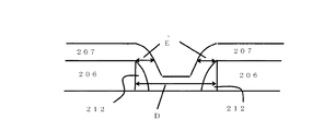
106、206、306、406 第1層目のアルミニウム膜(配線層)
107、207、407 第1層目の金属間絶縁膜
408 SOG膜
109、209、409 第2層目の金属間絶縁膜
110、210、410 SiN膜(保護膜)
311 開口領域
212 サイドスペーサー
B、D スペース幅
C、E 側壁厚さ
Claims (4)
- 半導体基板上に配置された素子分離絶縁膜と、
前記素子分離絶縁膜上に配置されたヒューズ素子と、
前記ヒューズ素子上に配置された絶縁膜と、
前記絶縁膜に設けられた接続孔を介して前記ヒューズ素子に接続される第1配線層と、
前記第1配線層とその上方に配置された第2配線層との間に設けられた、平坦化された第1金属間絶縁膜および第2金属間絶縁膜と、
前記第2金属間絶縁膜の上に設けられた保護膜と、
を有する半導体集積回路装置であって、
前記保護膜は前記ヒューズ素子上方に開口領域を有しており、
隣り合う前記ヒューズ素子に接続される前記第1配線層間のスペース幅を前記第1金属間絶縁膜の側壁厚さの2倍未満とし、前記開口領域の内側に露出する前記第1配線層間が前記第1金属絶縁層のみで埋め込まれていることを特徴とする半導体集積回路装置。 - 半導体基板上に配置された素子分離絶縁膜と、
前記素子分離絶縁膜上に配置されたヒューズ素子と、
前記ヒューズ素子上に配置された絶縁膜と、
前記絶縁膜に設けられた接続孔を介して前記ヒューズ素子に接続される第1配線層と、
前記第1配線層とその上方に配置された第2配線層との間に設けられた、平坦化された第1金属間絶縁膜および第2金属間絶縁膜と、
前記第2金属間絶縁膜の上に設けられた保護膜と、
を有する半導体集積回路装置であって、
前記保護膜は前記ヒューズ素子上方に開口領域を有し、
前記第1配線層の側面にサイドスペーサーを有し、
隣り合う前記ヒューズ素子に接続される前記第1配線層間のスペース幅を、前記サイドスペーサーを形成するための絶縁膜の側壁厚さの2倍未満とし、前記開口領域の内側に露出する前記第1配線層間が前記第1金属絶縁層のみで埋め込まれていることを特徴とする半導体集積回路装置。 - 前記サイドスペーサーは、シリコン酸化膜あるいはリン珪酸ガラス(PSG)膜あるいはシリコン窒化膜であることを特徴とする請求項2記載の半導体集積回路装置。
- 半導体基板上に素子分離絶縁膜を設ける工程と、
前記素子分離絶縁膜上にヒューズ素子を設ける工程と、
前記ヒューズ素子上に絶縁膜を設ける工程と、
前記絶縁膜に接続孔を介して前記ヒューズ素子に接続される第1配線層を、隣り合う前記ヒューズ素子に接続される前記第1配線層間のスペース幅を前記絶縁膜の側壁厚さの2倍未満となるよう設ける工程と、
前記第1配線層の側面にサイドスペーサーを形成する工程と、
前記第1配線層および前記サイドスペーサーを覆うように第1金属間絶縁膜を形成する工程と、
前記第1金属間絶縁膜の上にSOGを設けてからエッチバックにより前記第1金属間絶縁膜を平坦化し、その上に第2金属間絶縁膜を設ける工程と、
前記第2金属間絶縁膜の上に保護膜を形成する工程と、
前記ヒューズ素子上方の前記保護膜に開口領域を、前記開口領域の内側に前記第1配線層および前記第1配線層間に埋め込まれた第1金属絶縁層が露出するように形成する工程と、
を有する半導体集積回路装置の製造方法。
Priority Applications (5)
| Application Number | Priority Date | Filing Date | Title |
|---|---|---|---|
| JP2009221238A JP5507178B2 (ja) | 2009-09-25 | 2009-09-25 | 半導体集積回路装置およびその製造方法 |
| TW099130322A TWI555162B (zh) | 2009-09-25 | 2010-09-08 | 半導體積體電路裝置及其製造方法 |
| KR1020100090888A KR101663836B1 (ko) | 2009-09-25 | 2010-09-16 | 반도체 집적 회로 장치 및 그 제조 방법 |
| CN201010290650.6A CN102034791B (zh) | 2009-09-25 | 2010-09-21 | 半导体集成电路装置及其制造方法 |
| US12/888,183 US8324708B2 (en) | 2009-09-25 | 2010-09-22 | Semiconductor integrated circuit device and manufacturing method thereof |
Applications Claiming Priority (1)
| Application Number | Priority Date | Filing Date | Title |
|---|---|---|---|
| JP2009221238A JP5507178B2 (ja) | 2009-09-25 | 2009-09-25 | 半導体集積回路装置およびその製造方法 |
Publications (3)
| Publication Number | Publication Date |
|---|---|
| JP2011071324A JP2011071324A (ja) | 2011-04-07 |
| JP2011071324A5 JP2011071324A5 (ja) | 2012-08-30 |
| JP5507178B2 true JP5507178B2 (ja) | 2014-05-28 |
Family
ID=43779359
Family Applications (1)
| Application Number | Title | Priority Date | Filing Date |
|---|---|---|---|
| JP2009221238A Active JP5507178B2 (ja) | 2009-09-25 | 2009-09-25 | 半導体集積回路装置およびその製造方法 |
Country Status (5)
| Country | Link |
|---|---|
| US (1) | US8324708B2 (ja) |
| JP (1) | JP5507178B2 (ja) |
| KR (1) | KR101663836B1 (ja) |
| CN (1) | CN102034791B (ja) |
| TW (1) | TWI555162B (ja) |
Families Citing this family (7)
| Publication number | Priority date | Publication date | Assignee | Title |
|---|---|---|---|---|
| JP5981260B2 (ja) * | 2011-09-30 | 2016-08-31 | エスアイアイ・セミコンダクタ株式会社 | 半導体装置 |
| JP6620024B2 (ja) * | 2015-03-12 | 2019-12-11 | エイブリック株式会社 | 半導体装置 |
| JP6620023B2 (ja) * | 2015-03-12 | 2019-12-11 | エイブリック株式会社 | 半導体装置およびその製造方法 |
| US9917055B2 (en) * | 2015-03-12 | 2018-03-13 | Sii Semiconductor Corporation | Semiconductor device having fuse element |
| US9818691B2 (en) * | 2015-03-12 | 2017-11-14 | Sii Semiconductor Corporation | Semiconductor device having a fuse element |
| JP7158160B2 (ja) * | 2018-03-05 | 2022-10-21 | エイブリック株式会社 | 半導体装置 |
| JP6803595B1 (ja) * | 2020-09-16 | 2020-12-23 | アルディーテック株式会社 | 半導体発光素子チップ集積装置およびその製造方法 |
Family Cites Families (9)
| Publication number | Priority date | Publication date | Assignee | Title |
|---|---|---|---|---|
| JPH03171758A (ja) * | 1989-11-30 | 1991-07-25 | Nec Corp | 半導体装置及びその製造方法 |
| JPH0521605A (ja) * | 1991-07-12 | 1993-01-29 | Sony Corp | 半導体装置 |
| JPH0722508A (ja) * | 1993-06-24 | 1995-01-24 | Hitachi Ltd | 半導体集積回路装置 |
| JPH0737988A (ja) * | 1993-07-20 | 1995-02-07 | Hitachi Ltd | 半導体集積回路装置の製造方法 |
| JP3147149B2 (ja) * | 1997-02-07 | 2001-03-19 | 日本電気株式会社 | 半導体装置及びその製造方法 |
| US6589712B1 (en) * | 1998-11-04 | 2003-07-08 | Yi-Ren Hsu | Method for forming a passivation layer using polyimide layer as a mask |
| JP2002050692A (ja) * | 2000-08-01 | 2002-02-15 | Nec Corp | 半導体装置およびその製造方法 |
| CN100501973C (zh) * | 2005-03-30 | 2009-06-17 | 雅马哈株式会社 | 适合半导体器件的熔丝断开方法 |
| JP2010118427A (ja) * | 2008-11-12 | 2010-05-27 | Nec Electronics Corp | 半導体装置および半導体装置の製造方法 |
-
2009
- 2009-09-25 JP JP2009221238A patent/JP5507178B2/ja active Active
-
2010
- 2010-09-08 TW TW099130322A patent/TWI555162B/zh not_active IP Right Cessation
- 2010-09-16 KR KR1020100090888A patent/KR101663836B1/ko active IP Right Grant
- 2010-09-21 CN CN201010290650.6A patent/CN102034791B/zh not_active Expired - Fee Related
- 2010-09-22 US US12/888,183 patent/US8324708B2/en active Active
Also Published As
| Publication number | Publication date |
|---|---|
| JP2011071324A (ja) | 2011-04-07 |
| TWI555162B (zh) | 2016-10-21 |
| KR101663836B1 (ko) | 2016-10-14 |
| TW201125098A (en) | 2011-07-16 |
| KR20110033785A (ko) | 2011-03-31 |
| US20110073986A1 (en) | 2011-03-31 |
| US8324708B2 (en) | 2012-12-04 |
| CN102034791A (zh) | 2011-04-27 |
| CN102034791B (zh) | 2016-02-24 |
Similar Documents
| Publication | Publication Date | Title |
|---|---|---|
| JP5507178B2 (ja) | 半導体集積回路装置およびその製造方法 | |
| TWI406339B (zh) | Semiconductor device and manufacturing method thereof | |
| JP6075114B2 (ja) | 半導体装置および半導体装置の製造方法 | |
| JP4118029B2 (ja) | 半導体集積回路装置とその製造方法 | |
| JP4360881B2 (ja) | 多層配線を含む半導体装置およびその製造方法 | |
| JP4434606B2 (ja) | 半導体装置、半導体装置の製造方法 | |
| KR100436674B1 (ko) | 반도체 장치 및 그 제조 방법 | |
| JPH10242204A (ja) | 半導体装置および半導体装置の製造方法 | |
| JP6872553B2 (ja) | 半導体装置、撮像装置、および半導体装置の製造方法 | |
| JP4280204B2 (ja) | 半導体装置 | |
| US20070007655A1 (en) | Semiconductor device | |
| JP4050876B2 (ja) | 半導体集積回路装置とその製造方法 | |
| JP2008282903A (ja) | 半導体装置およびその製造方法 | |
| JP2009295733A (ja) | 半導体装置及びその製造方法 | |
| US11728262B2 (en) | Metal plate corner structure on metal insulator metal | |
| TWI423329B (zh) | 保護層結構及其製作方法 | |
| JP2008300385A (ja) | 配線構造およびその製造方法 | |
| JP4891296B2 (ja) | 半導体集積回路装置の製造方法 | |
| JP2010206226A (ja) | 半導体装置の製造方法 | |
| KR20090055772A (ko) | 반도체 소자의 금속 배선 형성 방법 | |
| KR100628220B1 (ko) | 반도체 소자의 콘택 제조방법 | |
| WO2010113369A1 (ja) | 半導体装置の製造方法 | |
| KR100608367B1 (ko) | 금속배선의 형성방법 | |
| JP5722651B2 (ja) | 半導体装置およびその製造方法 | |
| KR100383084B1 (ko) | 반도체 소자의 플러그 형성 방법 |
Legal Events
| Date | Code | Title | Description |
|---|---|---|---|
| A521 | Written amendment |
Free format text: JAPANESE INTERMEDIATE CODE: A523 Effective date: 20120711 |
|
| A621 | Written request for application examination |
Free format text: JAPANESE INTERMEDIATE CODE: A621 Effective date: 20120711 |
|
| A977 | Report on retrieval |
Free format text: JAPANESE INTERMEDIATE CODE: A971007 Effective date: 20131206 |
|
| A131 | Notification of reasons for refusal |
Free format text: JAPANESE INTERMEDIATE CODE: A131 Effective date: 20131210 |
|
| A521 | Written amendment |
Free format text: JAPANESE INTERMEDIATE CODE: A523 Effective date: 20140206 |
|
| TRDD | Decision of grant or rejection written | ||
| A01 | Written decision to grant a patent or to grant a registration (utility model) |
Free format text: JAPANESE INTERMEDIATE CODE: A01 Effective date: 20140225 |
|
| A61 | First payment of annual fees (during grant procedure) |
Free format text: JAPANESE INTERMEDIATE CODE: A61 Effective date: 20140319 |
|
| R150 | Certificate of patent or registration of utility model |
Ref document number: 5507178 Country of ref document: JP Free format text: JAPANESE INTERMEDIATE CODE: R150 |
|
| S111 | Request for change of ownership or part of ownership |
Free format text: JAPANESE INTERMEDIATE CODE: R313113 |
|
| R350 | Written notification of registration of transfer |
Free format text: JAPANESE INTERMEDIATE CODE: R350 |
|
| R250 | Receipt of annual fees |
Free format text: JAPANESE INTERMEDIATE CODE: R250 |
|
| S533 | Written request for registration of change of name |
Free format text: JAPANESE INTERMEDIATE CODE: R313533 |
|
| R350 | Written notification of registration of transfer |
Free format text: JAPANESE INTERMEDIATE CODE: R350 |
|
| R250 | Receipt of annual fees |
Free format text: JAPANESE INTERMEDIATE CODE: R250 |
|
| R250 | Receipt of annual fees |
Free format text: JAPANESE INTERMEDIATE CODE: R250 |
|
| R250 | Receipt of annual fees |
Free format text: JAPANESE INTERMEDIATE CODE: R250 |