JP5367531B2 - Tg基体上の平滑層及びバリア層 - Google Patents
Tg基体上の平滑層及びバリア層 Download PDFInfo
- Publication number
- JP5367531B2 JP5367531B2 JP2009244705A JP2009244705A JP5367531B2 JP 5367531 B2 JP5367531 B2 JP 5367531B2 JP 2009244705 A JP2009244705 A JP 2009244705A JP 2009244705 A JP2009244705 A JP 2009244705A JP 5367531 B2 JP5367531 B2 JP 5367531B2
- Authority
- JP
- Japan
- Prior art keywords
- barrier
- layer
- polymer
- display device
- substrate
- Prior art date
- Legal status (The legal status is an assumption and is not a legal conclusion. Google has not performed a legal analysis and makes no representation as to the accuracy of the status listed.)
- Expired - Lifetime
Links
Images


Classifications
-
- B—PERFORMING OPERATIONS; TRANSPORTING
- B05—SPRAYING OR ATOMISING IN GENERAL; APPLYING FLUENT MATERIALS TO SURFACES, IN GENERAL
- B05D—PROCESSES FOR APPLYING FLUENT MATERIALS TO SURFACES, IN GENERAL
- B05D1/00—Processes for applying liquids or other fluent materials
- B05D1/60—Deposition of organic layers from vapour phase
-
- B—PERFORMING OPERATIONS; TRANSPORTING
- B32—LAYERED PRODUCTS
- B32B—LAYERED PRODUCTS, i.e. PRODUCTS BUILT-UP OF STRATA OF FLAT OR NON-FLAT, e.g. CELLULAR OR HONEYCOMB, FORM
- B32B27/00—Layered products comprising a layer of synthetic resin
- B32B27/06—Layered products comprising a layer of synthetic resin as the main or only constituent of a layer, which is next to another layer of the same or of a different material
- B32B27/08—Layered products comprising a layer of synthetic resin as the main or only constituent of a layer, which is next to another layer of the same or of a different material of synthetic resin
-
- B—PERFORMING OPERATIONS; TRANSPORTING
- B32—LAYERED PRODUCTS
- B32B—LAYERED PRODUCTS, i.e. PRODUCTS BUILT-UP OF STRATA OF FLAT OR NON-FLAT, e.g. CELLULAR OR HONEYCOMB, FORM
- B32B27/00—Layered products comprising a layer of synthetic resin
- B32B27/28—Layered products comprising a layer of synthetic resin comprising synthetic resins not wholly covered by any one of the sub-groups B32B27/30 - B32B27/42
- B32B27/281—Layered products comprising a layer of synthetic resin comprising synthetic resins not wholly covered by any one of the sub-groups B32B27/30 - B32B27/42 comprising polyimides
-
- B—PERFORMING OPERATIONS; TRANSPORTING
- B32—LAYERED PRODUCTS
- B32B—LAYERED PRODUCTS, i.e. PRODUCTS BUILT-UP OF STRATA OF FLAT OR NON-FLAT, e.g. CELLULAR OR HONEYCOMB, FORM
- B32B27/00—Layered products comprising a layer of synthetic resin
- B32B27/28—Layered products comprising a layer of synthetic resin comprising synthetic resins not wholly covered by any one of the sub-groups B32B27/30 - B32B27/42
- B32B27/286—Layered products comprising a layer of synthetic resin comprising synthetic resins not wholly covered by any one of the sub-groups B32B27/30 - B32B27/42 comprising polysulphones; polysulfides
-
- B—PERFORMING OPERATIONS; TRANSPORTING
- B32—LAYERED PRODUCTS
- B32B—LAYERED PRODUCTS, i.e. PRODUCTS BUILT-UP OF STRATA OF FLAT OR NON-FLAT, e.g. CELLULAR OR HONEYCOMB, FORM
- B32B27/00—Layered products comprising a layer of synthetic resin
- B32B27/32—Layered products comprising a layer of synthetic resin comprising polyolefins
- B32B27/325—Layered products comprising a layer of synthetic resin comprising polyolefins comprising polycycloolefins
-
- B—PERFORMING OPERATIONS; TRANSPORTING
- B32—LAYERED PRODUCTS
- B32B—LAYERED PRODUCTS, i.e. PRODUCTS BUILT-UP OF STRATA OF FLAT OR NON-FLAT, e.g. CELLULAR OR HONEYCOMB, FORM
- B32B27/00—Layered products comprising a layer of synthetic resin
- B32B27/34—Layered products comprising a layer of synthetic resin comprising polyamides
-
- B—PERFORMING OPERATIONS; TRANSPORTING
- B32—LAYERED PRODUCTS
- B32B—LAYERED PRODUCTS, i.e. PRODUCTS BUILT-UP OF STRATA OF FLAT OR NON-FLAT, e.g. CELLULAR OR HONEYCOMB, FORM
- B32B27/00—Layered products comprising a layer of synthetic resin
- B32B27/36—Layered products comprising a layer of synthetic resin comprising polyesters
- B32B27/365—Layered products comprising a layer of synthetic resin comprising polyesters comprising polycarbonates
-
- B—PERFORMING OPERATIONS; TRANSPORTING
- B32—LAYERED PRODUCTS
- B32B—LAYERED PRODUCTS, i.e. PRODUCTS BUILT-UP OF STRATA OF FLAT OR NON-FLAT, e.g. CELLULAR OR HONEYCOMB, FORM
- B32B7/00—Layered products characterised by the relation between layers; Layered products characterised by the relative orientation of features between layers, or by the relative values of a measurable parameter between layers, i.e. products comprising layers having different physical, chemical or physicochemical properties; Layered products characterised by the interconnection of layers
- B32B7/04—Interconnection of layers
- B32B7/12—Interconnection of layers using interposed adhesives or interposed materials with bonding properties
-
- H—ELECTRICITY
- H10—SEMICONDUCTOR DEVICES; ELECTRIC SOLID-STATE DEVICES NOT OTHERWISE PROVIDED FOR
- H10K—ORGANIC ELECTRIC SOLID-STATE DEVICES
- H10K50/00—Organic light-emitting devices
- H10K50/80—Constructional details
- H10K50/84—Passivation; Containers; Encapsulations
- H10K50/844—Encapsulations
- H10K50/8445—Encapsulations multilayered coatings having a repetitive structure, e.g. having multiple organic-inorganic bilayers
-
- B—PERFORMING OPERATIONS; TRANSPORTING
- B32—LAYERED PRODUCTS
- B32B—LAYERED PRODUCTS, i.e. PRODUCTS BUILT-UP OF STRATA OF FLAT OR NON-FLAT, e.g. CELLULAR OR HONEYCOMB, FORM
- B32B2307/00—Properties of the layers or laminate
- B32B2307/40—Properties of the layers or laminate having particular optical properties
- B32B2307/41—Opaque
-
- B—PERFORMING OPERATIONS; TRANSPORTING
- B32—LAYERED PRODUCTS
- B32B—LAYERED PRODUCTS, i.e. PRODUCTS BUILT-UP OF STRATA OF FLAT OR NON-FLAT, e.g. CELLULAR OR HONEYCOMB, FORM
- B32B2307/00—Properties of the layers or laminate
- B32B2307/40—Properties of the layers or laminate having particular optical properties
- B32B2307/412—Transparent
-
- B—PERFORMING OPERATIONS; TRANSPORTING
- B32—LAYERED PRODUCTS
- B32B—LAYERED PRODUCTS, i.e. PRODUCTS BUILT-UP OF STRATA OF FLAT OR NON-FLAT, e.g. CELLULAR OR HONEYCOMB, FORM
- B32B2307/00—Properties of the layers or laminate
- B32B2307/70—Other properties
- B32B2307/724—Permeability to gases, adsorption
- B32B2307/7242—Non-permeable
- B32B2307/7244—Oxygen barrier
-
- B—PERFORMING OPERATIONS; TRANSPORTING
- B32—LAYERED PRODUCTS
- B32B—LAYERED PRODUCTS, i.e. PRODUCTS BUILT-UP OF STRATA OF FLAT OR NON-FLAT, e.g. CELLULAR OR HONEYCOMB, FORM
- B32B2307/00—Properties of the layers or laminate
- B32B2307/70—Other properties
- B32B2307/724—Permeability to gases, adsorption
- B32B2307/7242—Non-permeable
- B32B2307/7246—Water vapor barrier
-
- B—PERFORMING OPERATIONS; TRANSPORTING
- B32—LAYERED PRODUCTS
- B32B—LAYERED PRODUCTS, i.e. PRODUCTS BUILT-UP OF STRATA OF FLAT OR NON-FLAT, e.g. CELLULAR OR HONEYCOMB, FORM
- B32B2323/00—Polyalkenes
-
- B—PERFORMING OPERATIONS; TRANSPORTING
- B32—LAYERED PRODUCTS
- B32B—LAYERED PRODUCTS, i.e. PRODUCTS BUILT-UP OF STRATA OF FLAT OR NON-FLAT, e.g. CELLULAR OR HONEYCOMB, FORM
- B32B2369/00—Polycarbonates
-
- B—PERFORMING OPERATIONS; TRANSPORTING
- B32—LAYERED PRODUCTS
- B32B—LAYERED PRODUCTS, i.e. PRODUCTS BUILT-UP OF STRATA OF FLAT OR NON-FLAT, e.g. CELLULAR OR HONEYCOMB, FORM
- B32B2377/00—Polyamides
-
- B—PERFORMING OPERATIONS; TRANSPORTING
- B32—LAYERED PRODUCTS
- B32B—LAYERED PRODUCTS, i.e. PRODUCTS BUILT-UP OF STRATA OF FLAT OR NON-FLAT, e.g. CELLULAR OR HONEYCOMB, FORM
- B32B2457/00—Electrical equipment
- B32B2457/20—Displays, e.g. liquid crystal displays, plasma displays
-
- H—ELECTRICITY
- H10—SEMICONDUCTOR DEVICES; ELECTRIC SOLID-STATE DEVICES NOT OTHERWISE PROVIDED FOR
- H10K—ORGANIC ELECTRIC SOLID-STATE DEVICES
- H10K59/00—Integrated devices, or assemblies of multiple devices, comprising at least one organic light-emitting element covered by group H10K50/00
- H10K59/80—Constructional details
- H10K59/87—Passivation; Containers; Encapsulations
- H10K59/873—Encapsulations
- H10K59/8731—Encapsulations multilayered coatings having a repetitive structure, e.g. having multiple organic-inorganic bilayers
-
- Y—GENERAL TAGGING OF NEW TECHNOLOGICAL DEVELOPMENTS; GENERAL TAGGING OF CROSS-SECTIONAL TECHNOLOGIES SPANNING OVER SEVERAL SECTIONS OF THE IPC; TECHNICAL SUBJECTS COVERED BY FORMER USPC CROSS-REFERENCE ART COLLECTIONS [XRACs] AND DIGESTS
- Y10—TECHNICAL SUBJECTS COVERED BY FORMER USPC
- Y10T—TECHNICAL SUBJECTS COVERED BY FORMER US CLASSIFICATION
- Y10T428/00—Stock material or miscellaneous articles
- Y10T428/31504—Composite [nonstructural laminate]
- Y10T428/31507—Of polycarbonate
-
- Y—GENERAL TAGGING OF NEW TECHNOLOGICAL DEVELOPMENTS; GENERAL TAGGING OF CROSS-SECTIONAL TECHNOLOGIES SPANNING OVER SEVERAL SECTIONS OF THE IPC; TECHNICAL SUBJECTS COVERED BY FORMER USPC CROSS-REFERENCE ART COLLECTIONS [XRACs] AND DIGESTS
- Y10—TECHNICAL SUBJECTS COVERED BY FORMER USPC
- Y10T—TECHNICAL SUBJECTS COVERED BY FORMER US CLASSIFICATION
- Y10T428/00—Stock material or miscellaneous articles
- Y10T428/31504—Composite [nonstructural laminate]
- Y10T428/31533—Of polythioether
-
- Y—GENERAL TAGGING OF NEW TECHNOLOGICAL DEVELOPMENTS; GENERAL TAGGING OF CROSS-SECTIONAL TECHNOLOGIES SPANNING OVER SEVERAL SECTIONS OF THE IPC; TECHNICAL SUBJECTS COVERED BY FORMER USPC CROSS-REFERENCE ART COLLECTIONS [XRACs] AND DIGESTS
- Y10—TECHNICAL SUBJECTS COVERED BY FORMER USPC
- Y10T—TECHNICAL SUBJECTS COVERED BY FORMER US CLASSIFICATION
- Y10T428/00—Stock material or miscellaneous articles
- Y10T428/31504—Composite [nonstructural laminate]
- Y10T428/31652—Of asbestos
- Y10T428/31667—Next to addition polymer from unsaturated monomers, or aldehyde or ketone condensation product
-
- Y—GENERAL TAGGING OF NEW TECHNOLOGICAL DEVELOPMENTS; GENERAL TAGGING OF CROSS-SECTIONAL TECHNOLOGIES SPANNING OVER SEVERAL SECTIONS OF THE IPC; TECHNICAL SUBJECTS COVERED BY FORMER USPC CROSS-REFERENCE ART COLLECTIONS [XRACs] AND DIGESTS
- Y10—TECHNICAL SUBJECTS COVERED BY FORMER USPC
- Y10T—TECHNICAL SUBJECTS COVERED BY FORMER US CLASSIFICATION
- Y10T428/00—Stock material or miscellaneous articles
- Y10T428/31504—Composite [nonstructural laminate]
- Y10T428/31678—Of metal
-
- Y—GENERAL TAGGING OF NEW TECHNOLOGICAL DEVELOPMENTS; GENERAL TAGGING OF CROSS-SECTIONAL TECHNOLOGIES SPANNING OVER SEVERAL SECTIONS OF THE IPC; TECHNICAL SUBJECTS COVERED BY FORMER USPC CROSS-REFERENCE ART COLLECTIONS [XRACs] AND DIGESTS
- Y10—TECHNICAL SUBJECTS COVERED BY FORMER USPC
- Y10T—TECHNICAL SUBJECTS COVERED BY FORMER US CLASSIFICATION
- Y10T428/00—Stock material or miscellaneous articles
- Y10T428/31504—Composite [nonstructural laminate]
- Y10T428/31721—Of polyimide
-
- Y—GENERAL TAGGING OF NEW TECHNOLOGICAL DEVELOPMENTS; GENERAL TAGGING OF CROSS-SECTIONAL TECHNOLOGIES SPANNING OVER SEVERAL SECTIONS OF THE IPC; TECHNICAL SUBJECTS COVERED BY FORMER USPC CROSS-REFERENCE ART COLLECTIONS [XRACs] AND DIGESTS
- Y10—TECHNICAL SUBJECTS COVERED BY FORMER USPC
- Y10T—TECHNICAL SUBJECTS COVERED BY FORMER US CLASSIFICATION
- Y10T428/00—Stock material or miscellaneous articles
- Y10T428/31504—Composite [nonstructural laminate]
- Y10T428/31855—Of addition polymer from unsaturated monomers
- Y10T428/31935—Ester, halide or nitrile of addition polymer
Landscapes
- Chemical & Material Sciences (AREA)
- Inorganic Chemistry (AREA)
- Physics & Mathematics (AREA)
- Optics & Photonics (AREA)
- Laminated Bodies (AREA)
- Devices For Indicating Variable Information By Combining Individual Elements (AREA)
- Liquid Crystal (AREA)
Description
本発明は、さらに、改良された特性を有する高温基体を製造する方法も含む。この方法は、約120℃を超えるガラス転移点を有するポリマー基体を準備し、このポリマー基体上に少なくとも一つの第1バリアスタックを置くことを含む。バリアスタックは、少なくとも一つの第1バリア層と、少なくとも一つの第1ポリマー層と、を含む。
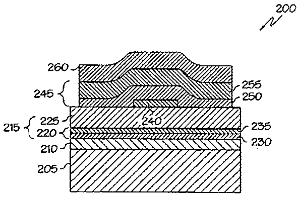
本発明の被包ディスプレイデバイスを図2に示す。被包ディスプレイデバイス200は、上述のように、基体205を含む。基体205の頂部には、ポリマー平滑層210がある。ポリマー平滑層210は、表面の粗さを減少させ、窪み、ひっかき傷及び掘痕などの表面欠陥を被包する。これは、後続層のデポジッションに理想的な平面化された表面を作り出す。所望の用途に応じて、有機層又は無機層、平面化層、電極層、ひっかき抵抗層、抗反射コーティング、及び他の機能層などの追加の層を基体205上にデポジットしてもよい。この態様において、基体は、異なる用途に対して、特別にあつらえることができる。
PETなどのポリマー性基体上の本発明のバリアスタックの酸素透過度(OTR)及び水蒸気透過度(WVTR)を測定したところ、浸透性測定として現在産業的に用いられている測定機器(Mocon OxTran 2/20L及びPermatran)の検出限界を良好に下回っていた。Table 1は、PET及びポリノルボルネン(PNB)上のいくつかのバリアスタックに対するMocon(Minneapolis, MN)で測定したOTR値及びWVTR値(それぞれASTM F 1927-98及びASTM F 1249-90に準拠して測定した)、及びいくつかの他の測定値を示す。
Claims (5)
- 改良された特性を有する高温基体であって
120℃を超えるガラス転移点を有するポリマー基体と、
該ポリマー基体の上に置かれた、少なくとも1の第1バリア層と該第1バリア層の上に置かれた少なくとも1の第1ポリマー層とを含む第1バリアスタックと、
前記ポリマー基体と前記第1バリアスタックとの間のポリマー平滑層と、
を含む高温基体と、
第1バリアスタックの上に置かれた環境感応性ディスプレイデバイスと、
該環境感応性ディスプレイデバイスの上に置かれた、少なくとも1の第2バリア層と該第2バリア層の上に置かれた少なくとも1の第2ポリマー層とを含む第2のバリアスタックであって、環境感応性ディスプレイデバイスを被包する、第2のバリアスタックと、
を含む被包ディスプレイデバイスであって、
該第1バリア層は、スパッタリング、化学蒸着、プラズマ強化化学蒸着、電子サイクロトロン共鳴プラズマ強化蒸着(ECR−PECVD)及びこれらの組合せにより蒸着され、該第1ポリマー層は真空蒸着されたアクリレート含有ポリマー層であり、
該第1バリアスタックを通過する酸素透過速度は、23℃、相対湿度0%で、0.005cc/m2/dayよりも低いことを特徴とする、被包ディスプレイデバイス。 - 前記ポリマー基体は、ポリノルボルネン、ポリイミド、ポリエーテルスルホン、ポリエーテルイミド、ポリカーボネート、及び高いガラス転移点を有する環式オレフィンポリマーから選択される請求項1に記載の被包ディスプレイデバイス。
- 前記第1バリア層は、金属酸化物、金属窒化物、金属炭化物、金属オキシナイトライド、金属オキシボライド及びこれらの組合せから選択される物質を含む請求項1又は2に記載の被包ディスプレイデバイス。
- 120℃を超えるガラス転移点を有するポリマー基体を準備する工程と、
前記ポリマー基体上にポリマー平滑層を堆積させる工程と、
該ポリマー平滑層の上に、少なくとも1の第1バリア層と該第1バリア層の上に置かれた少なくとも1の第1ポリマー層とを含む第1バリアスタックを置く工程と、
環境感応性ディスプレイデバイスを少なくとも1の第1バリアスタック上に置く工程と、
少なくとも1の第2バリア層と該第2バリア層の上に置かれた少なくとも1の第2ポリマー層とを含む第2バリアスタックを、該環境感応性ディスプレイデバイスの上方に置いて、環境感応性ディスプレイデバイスを被包する工程と、
を含み、
該第1バリア層は、スパッタリング、化学蒸着、プラズマ強化化学蒸着、電子サイクロトロン共鳴プラズマ強化蒸着(ECR−PECVD)及びこれらの組合せにより蒸着され、該第1ポリマー層は真空蒸着されたアクリレート含有ポリマー層であり、
該第1バリアスタックを通過する酸素透過速度は、23℃、相対湿度0%で、0.005cc/m2/dayよりも低い、改良された特性を有する被包ディスプレイデバイスを製造する方法。 - 環境感応性ディスプレイデバイスの上に少なくとも1の第2バリアスタックを置く工程は、少なくとも1の第2バリアスタックを環境感応性ディスプレイデバイス上にデポジットすることを含む請求項4記載の方法。
Applications Claiming Priority (2)
| Application Number | Priority Date | Filing Date | Title |
|---|---|---|---|
| US09/553,191 | 2000-04-20 | ||
| US09/553,191 US6492026B1 (en) | 2000-04-20 | 2000-04-20 | Smoothing and barrier layers on high Tg substrates |
Related Parent Applications (1)
| Application Number | Title | Priority Date | Filing Date |
|---|---|---|---|
| JP2001579332A Division JP2003531745A (ja) | 2000-04-20 | 2001-03-06 | Tg基体上の平滑層及びバリア層 |
Related Child Applications (1)
| Application Number | Title | Priority Date | Filing Date |
|---|---|---|---|
| JP2012214994A Division JP5436640B2 (ja) | 2000-04-20 | 2012-09-27 | Tg基体上の平滑層及びバリア層 |
Publications (2)
| Publication Number | Publication Date |
|---|---|
| JP2010058516A JP2010058516A (ja) | 2010-03-18 |
| JP5367531B2 true JP5367531B2 (ja) | 2013-12-11 |
Family
ID=24208472
Family Applications (3)
| Application Number | Title | Priority Date | Filing Date |
|---|---|---|---|
| JP2001579332A Withdrawn JP2003531745A (ja) | 2000-04-20 | 2001-03-06 | Tg基体上の平滑層及びバリア層 |
| JP2009244705A Expired - Lifetime JP5367531B2 (ja) | 2000-04-20 | 2009-10-23 | Tg基体上の平滑層及びバリア層 |
| JP2012214994A Expired - Lifetime JP5436640B2 (ja) | 2000-04-20 | 2012-09-27 | Tg基体上の平滑層及びバリア層 |
Family Applications Before (1)
| Application Number | Title | Priority Date | Filing Date |
|---|---|---|---|
| JP2001579332A Withdrawn JP2003531745A (ja) | 2000-04-20 | 2001-03-06 | Tg基体上の平滑層及びバリア層 |
Family Applications After (1)
| Application Number | Title | Priority Date | Filing Date |
|---|---|---|---|
| JP2012214994A Expired - Lifetime JP5436640B2 (ja) | 2000-04-20 | 2012-09-27 | Tg基体上の平滑層及びバリア層 |
Country Status (9)
| Country | Link |
|---|---|
| US (1) | US6492026B1 (ja) |
| EP (1) | EP1284835B1 (ja) |
| JP (3) | JP2003531745A (ja) |
| CN (1) | CN100365759C (ja) |
| AT (1) | ATE378129T1 (ja) |
| AU (1) | AU2001249090A1 (ja) |
| DE (1) | DE60131390T2 (ja) |
| TW (1) | TW575615B (ja) |
| WO (1) | WO2001082336A2 (ja) |
Families Citing this family (105)
| Publication number | Priority date | Publication date | Assignee | Title |
|---|---|---|---|---|
| US20040241454A1 (en) * | 1993-10-04 | 2004-12-02 | Shaw David G. | Barrier sheet and method of making same |
| EP1127381B1 (en) | 1998-11-02 | 2015-09-23 | 3M Innovative Properties Company | Transparent conductive oxides for plastic flat panel displays |
| US6207238B1 (en) | 1998-12-16 | 2001-03-27 | Battelle Memorial Institute | Plasma enhanced chemical deposition for high and/or low index of refraction polymers |
| US6228434B1 (en) | 1998-12-16 | 2001-05-08 | Battelle Memorial Institute | Method of making a conformal coating of a microtextured surface |
| US6228436B1 (en) | 1998-12-16 | 2001-05-08 | Battelle Memorial Institute | Method of making light emitting polymer composite material |
| US8853696B1 (en) | 1999-06-04 | 2014-10-07 | Semiconductor Energy Laboratory Co., Ltd. | Electro-optical device and electronic device |
| US6413645B1 (en) * | 2000-04-20 | 2002-07-02 | Battelle Memorial Institute | Ultrabarrier substrates |
| US6573652B1 (en) | 1999-10-25 | 2003-06-03 | Battelle Memorial Institute | Encapsulated display devices |
| US6623861B2 (en) | 2001-04-16 | 2003-09-23 | Battelle Memorial Institute | Multilayer plastic substrates |
| US7198832B2 (en) | 1999-10-25 | 2007-04-03 | Vitex Systems, Inc. | Method for edge sealing barrier films |
| US20100330748A1 (en) | 1999-10-25 | 2010-12-30 | Xi Chu | Method of encapsulating an environmentally sensitive device |
| US6866901B2 (en) | 1999-10-25 | 2005-03-15 | Vitex Systems, Inc. | Method for edge sealing barrier films |
| US6762124B2 (en) * | 2001-02-14 | 2004-07-13 | Avery Dennison Corporation | Method for patterning a multilayered conductor/substrate structure |
| JP4147008B2 (ja) * | 2001-03-05 | 2008-09-10 | 株式会社日立製作所 | 有機el素子に用いるフィルム及び有機el素子 |
| US8415208B2 (en) | 2001-07-16 | 2013-04-09 | Semiconductor Energy Laboratory Co., Ltd. | Semiconductor device and peeling off method and method of manufacturing semiconductor device |
| JP2003109773A (ja) * | 2001-07-27 | 2003-04-11 | Semiconductor Energy Lab Co Ltd | 発光装置、半導体装置およびそれらの作製方法 |
| JP5057619B2 (ja) | 2001-08-01 | 2012-10-24 | 株式会社半導体エネルギー研究所 | 半導体装置の作製方法 |
| TW554398B (en) * | 2001-08-10 | 2003-09-21 | Semiconductor Energy Lab | Method of peeling off and method of manufacturing semiconductor device |
| TW558743B (en) | 2001-08-22 | 2003-10-21 | Semiconductor Energy Lab | Peeling method and method of manufacturing semiconductor device |
| KR100944886B1 (ko) * | 2001-10-30 | 2010-03-03 | 가부시키가이샤 한도오따이 에네루기 켄큐쇼 | 반도체 장치의 제조 방법 |
| TWI264121B (en) | 2001-11-30 | 2006-10-11 | Semiconductor Energy Lab | A display device, a method of manufacturing a semiconductor device, and a method of manufacturing a display device |
| US6853785B2 (en) | 2001-12-14 | 2005-02-08 | 3M Innovative Properties Co. | Index modulation in glass using a femtosecond laser |
| JP2003282238A (ja) * | 2002-03-25 | 2003-10-03 | Pioneer Electronic Corp | 有機エレクトロルミネッセンス表示パネル及び製造方法 |
| US8808457B2 (en) | 2002-04-15 | 2014-08-19 | Samsung Display Co., Ltd. | Apparatus for depositing a multilayer coating on discrete sheets |
| US8900366B2 (en) | 2002-04-15 | 2014-12-02 | Samsung Display Co., Ltd. | Apparatus for depositing a multilayer coating on discrete sheets |
| US20040166335A1 (en) * | 2002-08-06 | 2004-08-26 | O'regan Marie B. | Laminated polymer with integrated lighting, sensors and electronics |
| US6929864B2 (en) | 2002-08-17 | 2005-08-16 | 3M Innovative Properties Company | Extensible, visible light-transmissive and infrared-reflective film and methods of making and using the film |
| US6933051B2 (en) | 2002-08-17 | 2005-08-23 | 3M Innovative Properties Company | Flexible electrically conductive film |
| US7215473B2 (en) * | 2002-08-17 | 2007-05-08 | 3M Innovative Properties Company | Enhanced heat mirror films |
| US8704211B2 (en) * | 2004-06-30 | 2014-04-22 | General Electric Company | High integrity protective coatings |
| US7015640B2 (en) | 2002-09-11 | 2006-03-21 | General Electric Company | Diffusion barrier coatings having graded compositions and devices incorporating the same |
| US20040229051A1 (en) | 2003-05-15 | 2004-11-18 | General Electric Company | Multilayer coating package on flexible substrates for electro-optical devices |
| US8691371B2 (en) * | 2002-09-11 | 2014-04-08 | General Electric Company | Barrier coating and method |
| US20050181212A1 (en) * | 2004-02-17 | 2005-08-18 | General Electric Company | Composite articles having diffusion barriers and devices incorporating the same |
| JP4693411B2 (ja) | 2002-10-30 | 2011-06-01 | 株式会社半導体エネルギー研究所 | 半導体装置の作製方法 |
| DE10255822B4 (de) * | 2002-11-29 | 2004-10-28 | Fraunhofer-Gesellschaft zur Förderung der angewandten Forschung e.V. | Verfahren zum Bedampfen bandförmiger Substrate mit einer transparenten Barriereschicht aus Aluminiumoxid |
| WO2004057919A1 (en) * | 2002-12-20 | 2004-07-08 | Ifire Technology Corp. | Barrier layer for thick film dielectric electroluminescent displays |
| US7229703B2 (en) * | 2003-03-31 | 2007-06-12 | Dai Nippon Printing Co. Ltd. | Gas barrier substrate |
| US7018713B2 (en) * | 2003-04-02 | 2006-03-28 | 3M Innovative Properties Company | Flexible high-temperature ultrabarrier |
| US7510913B2 (en) | 2003-04-11 | 2009-03-31 | Vitex Systems, Inc. | Method of making an encapsulated plasma sensitive device |
| US7648925B2 (en) | 2003-04-11 | 2010-01-19 | Vitex Systems, Inc. | Multilayer barrier stacks and methods of making multilayer barrier stacks |
| JP4617086B2 (ja) * | 2003-09-26 | 2011-01-19 | 大日本印刷株式会社 | 難燃性フィルム及びそれを用いた住宅用内装材、電気製品又は印刷用フィルム |
| US7297414B2 (en) * | 2003-09-30 | 2007-11-20 | Fujifilm Corporation | Gas barrier film and method for producing the same |
| US7635525B2 (en) * | 2003-09-30 | 2009-12-22 | Fujifilm Corporation | Gas barrier laminate film and method for producing the same |
| JP4233433B2 (ja) * | 2003-11-06 | 2009-03-04 | シャープ株式会社 | 表示装置の製造方法 |
| JP4313221B2 (ja) * | 2004-02-17 | 2009-08-12 | 富士フイルム株式会社 | ガスバリアフィルム |
| US20050202263A1 (en) * | 2004-03-09 | 2005-09-15 | Jonathan Sargent | Barrier layer to prevent the loss of additives in an underlying layer |
| US20050228465A1 (en) * | 2004-04-09 | 2005-10-13 | Christa Harris | Thermal device for activatable thermochemical compositions |
| JP2006007624A (ja) * | 2004-06-28 | 2006-01-12 | Dainippon Printing Co Ltd | ガスバリア性フィルム、並びにこれを用いたディスプレイ用基板及びカラーフィルタ |
| KR100615229B1 (ko) * | 2004-06-29 | 2006-08-25 | 삼성에스디아이 주식회사 | 박막 트랜지스터, 상기 박막 트랜지스터를 구비한 평판디스플레이 장치 및 상기 박막 트랜지스터의 제조방법 |
| US20060063015A1 (en) * | 2004-09-23 | 2006-03-23 | 3M Innovative Properties Company | Protected polymeric film |
| JP4716773B2 (ja) * | 2005-04-06 | 2011-07-06 | 富士フイルム株式会社 | ガスバリアフィルムとそれを用いた有機デバイス |
| US20060240275A1 (en) * | 2005-04-25 | 2006-10-26 | Gadkaree Kishor P | Flexible display substrates |
| US20070020451A1 (en) * | 2005-07-20 | 2007-01-25 | 3M Innovative Properties Company | Moisture barrier coatings |
| US7829147B2 (en) | 2005-08-18 | 2010-11-09 | Corning Incorporated | Hermetically sealing a device without a heat treating step and the resulting hermetically sealed device |
| US20070040501A1 (en) | 2005-08-18 | 2007-02-22 | Aitken Bruce G | Method for inhibiting oxygen and moisture degradation of a device and the resulting device |
| US7722929B2 (en) | 2005-08-18 | 2010-05-25 | Corning Incorporated | Sealing technique for decreasing the time it takes to hermetically seal a device and the resulting hermetically sealed device |
| US7767498B2 (en) | 2005-08-25 | 2010-08-03 | Vitex Systems, Inc. | Encapsulated devices and method of making |
| US20080006819A1 (en) * | 2006-06-19 | 2008-01-10 | 3M Innovative Properties Company | Moisture barrier coatings for organic light emitting diode devices |
| US7678701B2 (en) * | 2006-07-31 | 2010-03-16 | Eastman Kodak Company | Flexible substrate with electronic devices formed thereon |
| US7977170B2 (en) * | 2006-10-03 | 2011-07-12 | Eastman Kodak Company | Flexible substrate with electronic devices and traces |
| US8115326B2 (en) | 2006-11-30 | 2012-02-14 | Corning Incorporated | Flexible substrates having a thin-film barrier |
| WO2008083308A1 (en) | 2006-12-28 | 2008-07-10 | 3M Innovative Properties Company | Nucleation layer for thin film metal layer formation |
| CN101573471A (zh) * | 2006-12-29 | 2009-11-04 | 3M创新有限公司 | 固化含有金属烷氧化物的膜的方法 |
| BRPI0720867A2 (pt) * | 2006-12-29 | 2014-03-04 | 3M Innovative Properties Company. | Método para fabricação de filmes inorgânicos ou híbridos inorgânicos/orgânicos |
| US8241713B2 (en) * | 2007-02-21 | 2012-08-14 | 3M Innovative Properties Company | Moisture barrier coatings for organic light emitting diode devices |
| CN101668879B (zh) * | 2007-03-28 | 2012-05-09 | 陶氏康宁公司 | 含硅和碳的阻挡层的卷到卷等离子体增强化学气相沉积方法 |
| JP5296343B2 (ja) * | 2007-07-31 | 2013-09-25 | 住友化学株式会社 | バリア層つき基板、表示素子および表示素子の製造方法 |
| JP5162179B2 (ja) * | 2007-07-31 | 2013-03-13 | 住友化学株式会社 | 発光素子およびその製造方法並びに照明装置 |
| US8498464B2 (en) * | 2007-09-27 | 2013-07-30 | Siemens Medical Solutions Usa, Inc. | Intrinsic co-registration for modular multimodality medical imaging systems |
| CN104327758A (zh) | 2007-12-28 | 2015-02-04 | 3M创新有限公司 | 柔性封装膜系统 |
| US9627420B2 (en) * | 2008-02-08 | 2017-04-18 | Carestream Health, Inc. | Method for forming an electronic device on a flexible substrate supported by a detachable carrier |
| US8800138B2 (en) * | 2008-02-08 | 2014-08-12 | Carestream Health, Inc. | Method for conditioning a substrate surface for forming an electronic device thereon and resultant device |
| US7743492B2 (en) * | 2008-02-08 | 2010-06-29 | Carestream Health, Inc. | Method for forming cast flexible substrate and resultant substrate and electronic device |
| US8350451B2 (en) | 2008-06-05 | 2013-01-08 | 3M Innovative Properties Company | Ultrathin transparent EMI shielding film comprising a polymer basecoat and crosslinked polymer transparent dielectric layer |
| JP5624033B2 (ja) | 2008-06-30 | 2014-11-12 | スリーエム イノベイティブプロパティズカンパニー | 無機又は無機/有機ハイブリッドバリアフィルムの製造方法 |
| KR102383642B1 (ko) | 2008-07-10 | 2022-04-08 | 가부시키가이샤 한도오따이 에네루기 켄큐쇼 | 발광장치 및 전자기기 |
| JP5216716B2 (ja) | 2008-08-20 | 2013-06-19 | 株式会社半導体エネルギー研究所 | 発光装置及びその作製方法 |
| JP5405075B2 (ja) * | 2008-09-24 | 2014-02-05 | 富士フイルム株式会社 | ガスバリア膜の形成方法およびガスバリア膜 |
| US8033885B2 (en) | 2008-09-30 | 2011-10-11 | General Electric Company | System and method for applying a conformal barrier coating with pretreating |
| JP2010093172A (ja) * | 2008-10-10 | 2010-04-22 | Fujifilm Corp | 封止デバイス |
| JP2011003522A (ja) | 2008-10-16 | 2011-01-06 | Semiconductor Energy Lab Co Ltd | フレキシブル発光装置、電子機器及びフレキシブル発光装置の作製方法 |
| US9184410B2 (en) | 2008-12-22 | 2015-11-10 | Samsung Display Co., Ltd. | Encapsulated white OLEDs having enhanced optical output |
| US9337446B2 (en) | 2008-12-22 | 2016-05-10 | Samsung Display Co., Ltd. | Encapsulated RGB OLEDs having enhanced optical output |
| US8427845B2 (en) * | 2009-05-21 | 2013-04-23 | General Electric Company | Electrical connectors for optoelectronic device packaging |
| US20100294526A1 (en) * | 2009-05-21 | 2010-11-25 | General Electric Company | Hermetic electrical package |
| US8450926B2 (en) | 2009-05-21 | 2013-05-28 | General Electric Company | OLED lighting devices including electrodes with magnetic material |
| US8590338B2 (en) | 2009-12-31 | 2013-11-26 | Samsung Mobile Display Co., Ltd. | Evaporator with internal restriction |
| MX2012007950A (es) * | 2010-01-06 | 2012-08-01 | Dow Global Technologies Llc | Dispositivos fotovoltaicos resistentes a la humedad con capa de proteccion elastomerica de polisiloxano. |
| TWI589042B (zh) | 2010-01-20 | 2017-06-21 | 半導體能源研究所股份有限公司 | 發光裝置,撓性發光裝置,電子裝置,照明設備,以及發光裝置和撓性發光裝置的製造方法 |
| US9000442B2 (en) * | 2010-01-20 | 2015-04-07 | Semiconductor Energy Laboratory Co., Ltd. | Light-emitting device, flexible light-emitting device, electronic device, and method for manufacturing light-emitting device and flexible-light emitting device |
| CN102477531B (zh) * | 2010-11-26 | 2015-03-25 | 鸿富锦精密工业(深圳)有限公司 | 被覆件及其制造方法 |
| WO2013019698A1 (en) * | 2011-08-04 | 2013-02-07 | 3M Innovative Properties Company | Edge protected barrier assemblies |
| WO2013019695A2 (en) | 2011-08-04 | 2013-02-07 | 3M Innovative Properties Company | Edge protected barrier assemblies |
| US9362527B2 (en) | 2012-02-15 | 2016-06-07 | Konica Minolta, Inc. | Functional film having a hybrid layer of polysiloxane and fine resin particles |
| KR102079188B1 (ko) | 2012-05-09 | 2020-02-19 | 가부시키가이샤 한도오따이 에네루기 켄큐쇼 | 발광 장치 및 전자 기기 |
| WO2014129519A1 (en) | 2013-02-20 | 2014-08-28 | Semiconductor Energy Laboratory Co., Ltd. | Peeling method, semiconductor device, and peeling apparatus |
| KR102098573B1 (ko) * | 2013-07-19 | 2020-05-27 | 삼성디스플레이 주식회사 | 표시패널 및 그 제조방법 |
| KR102165869B1 (ko) | 2013-10-21 | 2020-10-15 | 삼성디스플레이 주식회사 | 봉지 부재 및 이를 포함하는 표시 장치 |
| WO2015087192A1 (en) | 2013-12-12 | 2015-06-18 | Semiconductor Energy Laboratory Co., Ltd. | Peeling method and peeling apparatus |
| EP3186319A4 (en) | 2014-07-25 | 2018-04-18 | Kateeva, Inc. | Organic thin film ink compositions and methods |
| US20160056414A1 (en) * | 2014-08-21 | 2016-02-25 | Universal Display Corporation | Thin film permeation barrier system for substrates and devices and method of making the same |
| CN107922766A (zh) | 2015-08-31 | 2018-04-17 | 科迪华公司 | 基于二‑和单(甲基)丙烯酸酯的有机薄膜油墨组合物 |
| CN105552247B (zh) * | 2015-12-08 | 2018-10-26 | 上海天马微电子有限公司 | 复合基板、柔性显示装置及其制备方法 |
| KR102890273B1 (ko) | 2017-04-21 | 2025-11-21 | 카티바, 인크. | 유기 박막을 형성하기 위한 조성물 및 기술 |
Family Cites Families (84)
| Publication number | Priority date | Publication date | Assignee | Title |
|---|---|---|---|---|
| US3475307A (en) | 1965-02-04 | 1969-10-28 | Continental Can Co | Condensation of monomer vapors to increase polymerization rates in a glow discharge |
| FR1393629A (fr) | 1965-09-13 | 1965-03-26 | Continental Oil Co | Procédé et appareil pour enduire des feuilles en matières solides |
| US3607365A (en) | 1969-05-12 | 1971-09-21 | Minnesota Mining & Mfg | Vapor phase method of coating substrates with polymeric coating |
| US4098965A (en) | 1977-01-24 | 1978-07-04 | Polaroid Corporation | Flat batteries and method of making the same |
| JPS55129345A (en) | 1979-03-29 | 1980-10-07 | Ulvac Corp | Electron beam plate making method by vapor phase film formation and vapor phase development |
| US4581337A (en) | 1983-07-07 | 1986-04-08 | E. I. Du Pont De Nemours And Company | Polyether polyamines as linking agents for particle reagents useful in immunoassays |
| US5032461A (en) | 1983-12-19 | 1991-07-16 | Spectrum Control, Inc. | Method of making a multi-layered article |
| US4842893A (en) | 1983-12-19 | 1989-06-27 | Spectrum Control, Inc. | High speed process for coating substrates |
| EP0155823B1 (en) | 1984-03-21 | 1989-07-26 | Nihon Shinku Gijutsu Kabushiki Kaisha | Improvements in or relating to the covering of substrates with synthetic resin films |
| US4695618A (en) | 1986-05-23 | 1987-09-22 | Ameron, Inc. | Solventless polyurethane spray compositions and method for applying them |
| JP2530350B2 (ja) | 1986-06-23 | 1996-09-04 | スペクトラム コントロール,インコーポレイテッド | モノマ―流体のフラッシュ蒸発 |
| US4954371A (en) | 1986-06-23 | 1990-09-04 | Spectrum Control, Inc. | Flash evaporation of monomer fluids |
| JPH07105034B2 (ja) | 1986-11-28 | 1995-11-13 | 株式会社日立製作所 | 磁気記録体 |
| JP2627619B2 (ja) | 1987-07-13 | 1997-07-09 | 日本電信電話株式会社 | 有機非晶質膜作製方法 |
| US4847469A (en) | 1987-07-15 | 1989-07-11 | The Boc Group, Inc. | Controlled flow vaporizer |
| JPH01171856A (ja) * | 1987-12-26 | 1989-07-06 | Toray Ind Inc | 金属蒸着フィルム |
| JP2742057B2 (ja) | 1988-07-14 | 1998-04-22 | シャープ株式会社 | 薄膜elパネル |
| JPH02183230A (ja) | 1989-01-09 | 1990-07-17 | Sharp Corp | 有機非線形光学材料及びその製造方法 |
| US5189405A (en) | 1989-01-26 | 1993-02-23 | Sharp Kabushiki Kaisha | Thin film electroluminescent panel |
| JP2678055B2 (ja) | 1989-03-30 | 1997-11-17 | シャープ株式会社 | 有機化合物薄膜の製法 |
| US5792550A (en) | 1989-10-24 | 1998-08-11 | Flex Products, Inc. | Barrier film having high colorless transparency and method |
| US5036249A (en) | 1989-12-11 | 1991-07-30 | Molex Incorporated | Electroluminescent lamp panel and method of fabricating same |
| US5362328A (en) | 1990-07-06 | 1994-11-08 | Advanced Technology Materials, Inc. | Apparatus and method for delivering reagents in vapor form to a CVD reactor, incorporating a cleaning subsystem |
| US5711816A (en) | 1990-07-06 | 1998-01-27 | Advanced Technolgy Materials, Inc. | Source reagent liquid delivery apparatus, and chemical vapor deposition system comprising same |
| JP2755844B2 (ja) | 1991-09-30 | 1998-05-25 | シャープ株式会社 | プラスチック基板液晶表示素子 |
| US5372851A (en) | 1991-12-16 | 1994-12-13 | Matsushita Electric Industrial Co., Ltd. | Method of manufacturing a chemically adsorbed film |
| US5759329A (en) | 1992-01-06 | 1998-06-02 | Pilot Industries, Inc. | Fluoropolymer composite tube and method of preparation |
| JP2958186B2 (ja) | 1992-04-20 | 1999-10-06 | シャープ株式会社 | プラスチック基板液晶表示素子 |
| US5427638A (en) | 1992-06-04 | 1995-06-27 | Alliedsignal Inc. | Low temperature reaction bonding |
| GB9215928D0 (en) | 1992-07-27 | 1992-09-09 | Cambridge Display Tech Ltd | Manufacture of electroluminescent devices |
| US5260095A (en) | 1992-08-21 | 1993-11-09 | Battelle Memorial Institute | Vacuum deposition and curing of liquid monomers |
| DE4232390A1 (de) | 1992-09-26 | 1994-03-31 | Roehm Gmbh | Verfahren zum Erzeugen von siliciumoxidischen kratzfesten Schichten auf Kunststoffen durch Plasmabeschichtung |
| JPH06182935A (ja) | 1992-12-18 | 1994-07-05 | Bridgestone Corp | ガスバリア性ゴム積層物及びその製造方法 |
| US5440446A (en) | 1993-10-04 | 1995-08-08 | Catalina Coatings, Inc. | Acrylate coating material |
| ATE233939T1 (de) * | 1993-10-04 | 2003-03-15 | 3M Innovative Properties Co | Vernetztes acrylatbeschichtungsmaterial zur herstellung von kondensatordielektrika und sauerstoffbarrieren |
| US5654084A (en) | 1994-07-22 | 1997-08-05 | Martin Marietta Energy Systems, Inc. | Protective coatings for sensitive materials |
| EP0733470A4 (en) * | 1994-09-30 | 1997-08-27 | Kanegafuchi Chemical Ind | HEAT-RESISTANT LAMINATED OPTICAL PLASTIC SHEET AND PROCESS FOR PRODUCING THE SAME |
| DE4438359C2 (de) | 1994-10-27 | 2001-10-04 | Schott Glas | Behälter aus Kunststoff mit einer Sperrbeschichtung |
| US6083628A (en) | 1994-11-04 | 2000-07-04 | Sigma Laboratories Of Arizona, Inc. | Hybrid polymer film |
| JP3204356B2 (ja) * | 1994-12-14 | 2001-09-04 | 住友ベークライト株式会社 | 透明導電フイルム |
| US5607789A (en) | 1995-01-23 | 1997-03-04 | Duracell Inc. | Light transparent multilayer moisture barrier for electrochemical cell tester and cell employing same |
| US5620524A (en) | 1995-02-27 | 1997-04-15 | Fan; Chiko | Apparatus for fluid delivery in chemical vapor deposition systems |
| US5811183A (en) | 1995-04-06 | 1998-09-22 | Shaw; David G. | Acrylate polymer release coated sheet materials and method of production thereof |
| US5771562A (en) | 1995-05-02 | 1998-06-30 | Motorola, Inc. | Passivation of organic devices |
| US5554220A (en) | 1995-05-19 | 1996-09-10 | The Trustees Of Princeton University | Method and apparatus using organic vapor phase deposition for the growth of organic thin films with large optical non-linearities |
| JPH08325713A (ja) | 1995-05-30 | 1996-12-10 | Matsushita Electric Works Ltd | 有機質基材表面への金属膜形成方法 |
| US5629389A (en) | 1995-06-06 | 1997-05-13 | Hewlett-Packard Company | Polymer-based electroluminescent device with improved stability |
| US5714199A (en) * | 1995-06-07 | 1998-02-03 | Libbey-Owens-Ford Co. | Method for applying a polymer powder onto a pre-heated glass substrate and the resulting article |
| BR9609594A (pt) | 1995-06-30 | 1999-02-23 | Commw Scient Ind Res Org | Tratamento melhorado da superfície de polímeros |
| US5681615A (en) | 1995-07-27 | 1997-10-28 | Battelle Memorial Institute | Vacuum flash evaporated polymer composites |
| JPH0959763A (ja) | 1995-08-25 | 1997-03-04 | Matsushita Electric Works Ltd | 有機質基材表面への金属膜形成方法 |
| JPH0957894A (ja) * | 1995-08-29 | 1997-03-04 | Fujimori Kogyo Kk | 透明電極付き光学用シート |
| US5723219A (en) | 1995-12-19 | 1998-03-03 | Talison Research | Plasma deposited film networks |
| DE19603746A1 (de) | 1995-10-20 | 1997-04-24 | Bosch Gmbh Robert | Elektrolumineszierendes Schichtsystem |
| US5811177A (en) | 1995-11-30 | 1998-09-22 | Motorola, Inc. | Passivation of electroluminescent organic devices |
| US5686360A (en) | 1995-11-30 | 1997-11-11 | Motorola | Passivation of organic devices |
| US5684084A (en) | 1995-12-21 | 1997-11-04 | E. I. Du Pont De Nemours And Company | Coating containing acrylosilane polymer to improve mar and acid etch resistance |
| US5955161A (en) | 1996-01-30 | 1999-09-21 | Becton Dickinson And Company | Blood collection tube assembly |
| US5731661A (en) | 1996-07-15 | 1998-03-24 | Motorola, Inc. | Passivation of electroluminescent organic devices |
| US5902688A (en) | 1996-07-16 | 1999-05-11 | Hewlett-Packard Company | Electroluminescent display device |
| US5693956A (en) | 1996-07-29 | 1997-12-02 | Motorola | Inverted oleds on hard plastic substrate |
| US5844363A (en) | 1997-01-23 | 1998-12-01 | The Trustees Of Princeton Univ. | Vacuum deposited, non-polymeric flexible organic light emitting devices |
| US5948552A (en) | 1996-08-27 | 1999-09-07 | Hewlett-Packard Company | Heat-resistant organic electroluminescent device |
| WO1998010116A1 (en) | 1996-09-05 | 1998-03-12 | Talison Research | Ultrasonic nozzle feed for plasma deposited film networks |
| JPH10119170A (ja) * | 1996-10-18 | 1998-05-12 | Sumitomo Bakelite Co Ltd | 可とう性積層フィルム |
| KR19980033213A (ko) | 1996-10-31 | 1998-07-25 | 조셉제이.스위니 | 스퍼터링 챔버내의 미립자 물질 발생 감소 방법 |
| US5821692A (en) | 1996-11-26 | 1998-10-13 | Motorola, Inc. | Organic electroluminescent device hermetic encapsulation package |
| US5912069A (en) | 1996-12-19 | 1999-06-15 | Sigma Laboratories Of Arizona | Metal nanolaminate composite |
| US5952778A (en) | 1997-03-18 | 1999-09-14 | International Business Machines Corporation | Encapsulated organic light emitting device |
| US5872355A (en) | 1997-04-09 | 1999-02-16 | Hewlett-Packard Company | Electroluminescent device and fabrication method for a light detection system |
| JP3290375B2 (ja) | 1997-05-12 | 2002-06-10 | 松下電器産業株式会社 | 有機電界発光素子 |
| US5994174A (en) * | 1997-09-29 | 1999-11-30 | The Regents Of The University Of California | Method of fabrication of display pixels driven by silicon thin film transistors |
| US5902641A (en) | 1997-09-29 | 1999-05-11 | Battelle Memorial Institute | Flash evaporation of liquid monomer particle mixture |
| US5965907A (en) | 1997-09-29 | 1999-10-12 | Motorola, Inc. | Full color organic light emitting backlight device for liquid crystal display applications |
| US6224948B1 (en) | 1997-09-29 | 2001-05-01 | Battelle Memorial Institute | Plasma enhanced chemical deposition with low vapor pressure compounds |
| US6194487B1 (en) | 1997-11-14 | 2001-02-27 | Sharp Kabushiki Kaisha | Method of manufacturing modified particles |
| JP3400324B2 (ja) * | 1997-11-17 | 2003-04-28 | 住友ベークライト株式会社 | 導電性フィルム |
| US6045864A (en) | 1997-12-01 | 2000-04-04 | 3M Innovative Properties Company | Vapor coating method |
| DE19802740A1 (de) | 1998-01-26 | 1999-07-29 | Leybold Systems Gmbh | Verfahren zur Behandlung von Oberflächen von Substraten aus Kunststoff |
| US5996498A (en) | 1998-03-12 | 1999-12-07 | Presstek, Inc. | Method of lithographic imaging with reduced debris-generated performance degradation and related constructions |
| US5904958A (en) | 1998-03-20 | 1999-05-18 | Rexam Industries Corp. | Adjustable nozzle for evaporation or organic monomers |
| JP4314642B2 (ja) * | 1998-04-30 | 2009-08-19 | 東洋紡績株式会社 | 真空蒸着用材料 |
| US6146225A (en) | 1998-07-30 | 2000-11-14 | Agilent Technologies, Inc. | Transparent, flexible permeability barrier for organic electroluminescent devices |
| JP3577232B2 (ja) * | 1999-01-22 | 2004-10-13 | シャープ株式会社 | 液晶表示素子 |
-
2000
- 2000-04-20 US US09/553,191 patent/US6492026B1/en not_active Expired - Lifetime
-
2001
- 2001-03-06 CN CNB018114911A patent/CN100365759C/zh not_active Expired - Lifetime
- 2001-03-06 AT AT01922271T patent/ATE378129T1/de not_active IP Right Cessation
- 2001-03-06 EP EP01922271A patent/EP1284835B1/en not_active Expired - Lifetime
- 2001-03-06 JP JP2001579332A patent/JP2003531745A/ja not_active Withdrawn
- 2001-03-06 DE DE60131390T patent/DE60131390T2/de not_active Expired - Lifetime
- 2001-03-06 AU AU2001249090A patent/AU2001249090A1/en not_active Abandoned
- 2001-03-06 WO PCT/US2001/007005 patent/WO2001082336A2/en not_active Ceased
- 2001-03-15 TW TW90106081A patent/TW575615B/zh not_active IP Right Cessation
-
2009
- 2009-10-23 JP JP2009244705A patent/JP5367531B2/ja not_active Expired - Lifetime
-
2012
- 2012-09-27 JP JP2012214994A patent/JP5436640B2/ja not_active Expired - Lifetime
Also Published As
| Publication number | Publication date |
|---|---|
| JP2003531745A (ja) | 2003-10-28 |
| DE60131390T2 (de) | 2008-09-25 |
| EP1284835A2 (en) | 2003-02-26 |
| US20020176993A1 (en) | 2002-11-28 |
| WO2001082336A3 (en) | 2002-12-05 |
| TW575615B (en) | 2004-02-11 |
| DE60131390D1 (de) | 2007-12-27 |
| CN1636258A (zh) | 2005-07-06 |
| ATE378129T1 (de) | 2007-11-15 |
| AU2001249090A1 (en) | 2001-11-07 |
| JP5436640B2 (ja) | 2014-03-05 |
| EP1284835B1 (en) | 2007-11-14 |
| WO2001082336A2 (en) | 2001-11-01 |
| JP2010058516A (ja) | 2010-03-18 |
| JP2013056546A (ja) | 2013-03-28 |
| US6492026B1 (en) | 2002-12-10 |
| CN100365759C (zh) | 2008-01-30 |
Similar Documents
| Publication | Publication Date | Title |
|---|---|---|
| JP5367531B2 (ja) | Tg基体上の平滑層及びバリア層 | |
| JP4115130B2 (ja) | 封入ディスプレーデバイス | |
| US6570325B2 (en) | Environmental barrier material for organic light emitting device and method of making | |
| JP5190525B2 (ja) | 有機発光デバイスのための環境バリヤー材料及びその製造方法 | |
| US6413645B1 (en) | Ultrabarrier substrates | |
| JP4750339B2 (ja) | 封入されたマイクロ電子デバイス | |
| WO2017033823A1 (ja) | 電子装置 |
Legal Events
| Date | Code | Title | Description |
|---|---|---|---|
| A711 | Notification of change in applicant |
Free format text: JAPANESE INTERMEDIATE CODE: A711 Effective date: 20110111 |
|
| A521 | Request for written amendment filed |
Free format text: JAPANESE INTERMEDIATE CODE: A821 Effective date: 20110111 |
|
| RD03 | Notification of appointment of power of attorney |
Free format text: JAPANESE INTERMEDIATE CODE: A7423 Effective date: 20110404 |
|
| A131 | Notification of reasons for refusal |
Free format text: JAPANESE INTERMEDIATE CODE: A131 Effective date: 20111025 |
|
| A521 | Request for written amendment filed |
Free format text: JAPANESE INTERMEDIATE CODE: A523 Effective date: 20120123 |
|
| RD04 | Notification of resignation of power of attorney |
Free format text: JAPANESE INTERMEDIATE CODE: A7424 Effective date: 20120307 |
|
| A02 | Decision of refusal |
Free format text: JAPANESE INTERMEDIATE CODE: A02 Effective date: 20120529 |
|
| A711 | Notification of change in applicant |
Free format text: JAPANESE INTERMEDIATE CODE: A712 Effective date: 20120921 |
|
| A521 | Request for written amendment filed |
Free format text: JAPANESE INTERMEDIATE CODE: A523 Effective date: 20120927 |
|
| A911 | Transfer to examiner for re-examination before appeal (zenchi) |
Free format text: JAPANESE INTERMEDIATE CODE: A911 Effective date: 20121019 |
|
| A912 | Re-examination (zenchi) completed and case transferred to appeal board |
Free format text: JAPANESE INTERMEDIATE CODE: A912 Effective date: 20121130 |
|
| A521 | Request for written amendment filed |
Free format text: JAPANESE INTERMEDIATE CODE: A523 Effective date: 20130725 |
|
| A61 | First payment of annual fees (during grant procedure) |
Free format text: JAPANESE INTERMEDIATE CODE: A61 Effective date: 20130911 |
|
| R150 | Certificate of patent or registration of utility model |
Ref document number: 5367531 Country of ref document: JP Free format text: JAPANESE INTERMEDIATE CODE: R150 Free format text: JAPANESE INTERMEDIATE CODE: R150 |
|
| R250 | Receipt of annual fees |
Free format text: JAPANESE INTERMEDIATE CODE: R250 |
|
| R250 | Receipt of annual fees |
Free format text: JAPANESE INTERMEDIATE CODE: R250 |
|
| R250 | Receipt of annual fees |
Free format text: JAPANESE INTERMEDIATE CODE: R250 |
|
| R250 | Receipt of annual fees |
Free format text: JAPANESE INTERMEDIATE CODE: R250 |
|
| R250 | Receipt of annual fees |
Free format text: JAPANESE INTERMEDIATE CODE: R250 |
|
| EXPY | Cancellation because of completion of term |