JP5183045B2 - 回路装置 - Google Patents
回路装置 Download PDFInfo
- Publication number
- JP5183045B2 JP5183045B2 JP2006228895A JP2006228895A JP5183045B2 JP 5183045 B2 JP5183045 B2 JP 5183045B2 JP 2006228895 A JP2006228895 A JP 2006228895A JP 2006228895 A JP2006228895 A JP 2006228895A JP 5183045 B2 JP5183045 B2 JP 5183045B2
- Authority
- JP
- Japan
- Prior art keywords
- insulating layer
- wiring
- conductive
- layer
- separation groove
- Prior art date
- Legal status (The legal status is an assumption and is not a legal conclusion. Google has not performed a legal analysis and makes no representation as to the accuracy of the status listed.)
- Expired - Fee Related
Links
- 239000010410 layer Substances 0.000 claims description 374
- 238000000926 separation method Methods 0.000 claims description 179
- 229910052751 metal Inorganic materials 0.000 claims description 65
- 239000002184 metal Substances 0.000 claims description 65
- 239000012792 core layer Substances 0.000 claims description 42
- 239000004065 semiconductor Substances 0.000 claims description 36
- 239000000758 substrate Substances 0.000 claims description 32
- 239000004020 conductor Substances 0.000 claims description 9
- RYGMFSIKBFXOCR-UHFFFAOYSA-N Copper Chemical compound [Cu] RYGMFSIKBFXOCR-UHFFFAOYSA-N 0.000 claims description 8
- 229910052802 copper Inorganic materials 0.000 claims description 7
- 239000010949 copper Substances 0.000 claims description 7
- 239000003822 epoxy resin Substances 0.000 claims description 5
- 229920000647 polyepoxide Polymers 0.000 claims description 5
- 239000011888 foil Substances 0.000 description 93
- 239000000463 material Substances 0.000 description 49
- 239000011229 interlayer Substances 0.000 description 47
- 238000000034 method Methods 0.000 description 43
- 238000004519 manufacturing process Methods 0.000 description 36
- 229920005989 resin Polymers 0.000 description 29
- 239000011347 resin Substances 0.000 description 29
- 238000005530 etching Methods 0.000 description 24
- 238000007747 plating Methods 0.000 description 18
- 229910000679 solder Inorganic materials 0.000 description 16
- 230000008569 process Effects 0.000 description 15
- 230000002093 peripheral effect Effects 0.000 description 13
- 238000001039 wet etching Methods 0.000 description 12
- 230000017525 heat dissipation Effects 0.000 description 11
- 238000007789 sealing Methods 0.000 description 6
- 239000007787 solid Substances 0.000 description 6
- 239000000945 filler Substances 0.000 description 5
- 238000009413 insulation Methods 0.000 description 4
- 230000000149 penetrating effect Effects 0.000 description 4
- 229910001111 Fine metal Inorganic materials 0.000 description 3
- 229910045601 alloy Inorganic materials 0.000 description 3
- 239000000956 alloy Substances 0.000 description 3
- 229910052782 aluminium Inorganic materials 0.000 description 3
- XAGFODPZIPBFFR-UHFFFAOYSA-N aluminium Chemical compound [Al] XAGFODPZIPBFFR-UHFFFAOYSA-N 0.000 description 3
- 230000015572 biosynthetic process Effects 0.000 description 3
- 239000003990 capacitor Substances 0.000 description 3
- 230000001678 irradiating effect Effects 0.000 description 3
- 229920005992 thermoplastic resin Polymers 0.000 description 3
- 229920001187 thermosetting polymer Polymers 0.000 description 3
- 238000013459 approach Methods 0.000 description 2
- 230000008859 change Effects 0.000 description 2
- 238000007772 electroless plating Methods 0.000 description 2
- 239000011521 glass Substances 0.000 description 2
- PCHJSUWPFVWCPO-UHFFFAOYSA-N gold Chemical compound [Au] PCHJSUWPFVWCPO-UHFFFAOYSA-N 0.000 description 2
- 239000010931 gold Substances 0.000 description 2
- 229910052737 gold Inorganic materials 0.000 description 2
- 239000007788 liquid Substances 0.000 description 2
- -1 made of aluminum Chemical compound 0.000 description 2
- 239000000203 mixture Substances 0.000 description 2
- 230000035515 penetration Effects 0.000 description 2
- 238000012545 processing Methods 0.000 description 2
- 239000004593 Epoxy Substances 0.000 description 1
- 229910052581 Si3N4 Inorganic materials 0.000 description 1
- VYPSYNLAJGMNEJ-UHFFFAOYSA-N Silicium dioxide Chemical compound O=[Si]=O VYPSYNLAJGMNEJ-UHFFFAOYSA-N 0.000 description 1
- 238000005299 abrasion Methods 0.000 description 1
- 239000000853 adhesive Substances 0.000 description 1
- 230000001070 adhesive effect Effects 0.000 description 1
- PNEYBMLMFCGWSK-UHFFFAOYSA-N aluminium oxide Inorganic materials [O-2].[O-2].[O-2].[Al+3].[Al+3] PNEYBMLMFCGWSK-UHFFFAOYSA-N 0.000 description 1
- 230000008901 benefit Effects 0.000 description 1
- 239000007767 bonding agent Substances 0.000 description 1
- 239000011889 copper foil Substances 0.000 description 1
- ORTQZVOHEJQUHG-UHFFFAOYSA-L copper(II) chloride Chemical compound Cl[Cu]Cl ORTQZVOHEJQUHG-UHFFFAOYSA-L 0.000 description 1
- 238000005520 cutting process Methods 0.000 description 1
- 230000002950 deficient Effects 0.000 description 1
- 238000011161 development Methods 0.000 description 1
- 238000005868 electrolysis reaction Methods 0.000 description 1
- 238000009713 electroplating Methods 0.000 description 1
- 230000020169 heat generation Effects 0.000 description 1
- 238000010438 heat treatment Methods 0.000 description 1
- 230000006872 improvement Effects 0.000 description 1
- 238000002347 injection Methods 0.000 description 1
- 239000007924 injection Substances 0.000 description 1
- FBAFATDZDUQKNH-UHFFFAOYSA-M iron chloride Chemical compound [Cl-].[Fe] FBAFATDZDUQKNH-UHFFFAOYSA-M 0.000 description 1
- 238000002955 isolation Methods 0.000 description 1
- 238000010329 laser etching Methods 0.000 description 1
- 239000007769 metal material Substances 0.000 description 1
- 229920013716 polyethylene resin Polymers 0.000 description 1
- 238000005096 rolling process Methods 0.000 description 1
- HQVNEWCFYHHQES-UHFFFAOYSA-N silicon nitride Chemical compound N12[Si]34N5[Si]62N3[Si]51N64 HQVNEWCFYHHQES-UHFFFAOYSA-N 0.000 description 1
- 229910052814 silicon oxide Inorganic materials 0.000 description 1
- 239000000243 solution Substances 0.000 description 1
- 238000012546 transfer Methods 0.000 description 1
Images


Landscapes
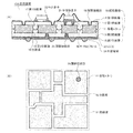
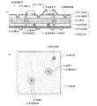
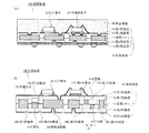
- Insulated Metal Substrates For Printed Circuits (AREA)
Priority Applications (1)
| Application Number | Priority Date | Filing Date | Title |
|---|---|---|---|
| JP2006228895A JP5183045B2 (ja) | 2006-07-20 | 2006-08-25 | 回路装置 |
Applications Claiming Priority (3)
| Application Number | Priority Date | Filing Date | Title |
|---|---|---|---|
| JP2006198782 | 2006-07-20 | ||
| JP2006198782 | 2006-07-20 | ||
| JP2006228895A JP5183045B2 (ja) | 2006-07-20 | 2006-08-25 | 回路装置 |
Publications (3)
| Publication Number | Publication Date |
|---|---|
| JP2008047843A JP2008047843A (ja) | 2008-02-28 |
| JP2008047843A5 JP2008047843A5 (enExample) | 2009-09-24 |
| JP5183045B2 true JP5183045B2 (ja) | 2013-04-17 |
Family
ID=39181254
Family Applications (1)
| Application Number | Title | Priority Date | Filing Date |
|---|---|---|---|
| JP2006228895A Expired - Fee Related JP5183045B2 (ja) | 2006-07-20 | 2006-08-25 | 回路装置 |
Country Status (1)
| Country | Link |
|---|---|
| JP (1) | JP5183045B2 (enExample) |
Families Citing this family (10)
| Publication number | Priority date | Publication date | Assignee | Title |
|---|---|---|---|---|
| JP5517927B2 (ja) * | 2008-05-29 | 2014-06-11 | 電気化学工業株式会社 | 金属ベース回路基板 |
| JP5184319B2 (ja) * | 2008-12-03 | 2013-04-17 | 株式会社オートネットワーク技術研究所 | 回路構成体及び回路構成体の製造方法 |
| JP2012028511A (ja) * | 2010-07-22 | 2012-02-09 | On Semiconductor Trading Ltd | 回路基板およびその製造方法、回路装置およびその製造方法、絶縁層付き導電箔 |
| JP2012114217A (ja) * | 2010-11-24 | 2012-06-14 | Nitto Denko Corp | 配線回路基板の製造方法 |
| TWI542260B (zh) * | 2010-12-24 | 2016-07-11 | Lg伊諾特股份有限公司 | 印刷電路板及其製造方法 |
| KR101865124B1 (ko) * | 2011-12-27 | 2018-06-08 | 해성디에스 주식회사 | 비아홀을 구비하지 않은 회로 기판 및 그 제조방법 |
| KR102435124B1 (ko) * | 2015-10-07 | 2022-08-24 | 삼성전기주식회사 | 인쇄회로기판 및 인쇄회로기판의 제조방법 |
| WO2018181678A1 (ja) * | 2017-03-30 | 2018-10-04 | 太陽誘電株式会社 | 配線基板及びその製造方法 |
| JP7069082B2 (ja) | 2019-05-08 | 2022-05-17 | 三菱電機株式会社 | 電力用半導体装置およびその製造方法 |
| JP2023069418A (ja) * | 2021-11-05 | 2023-05-18 | 日東電工株式会社 | 再配線基板およびその製造方法 |
Family Cites Families (13)
| Publication number | Priority date | Publication date | Assignee | Title |
|---|---|---|---|---|
| JPS6372180A (ja) * | 1986-09-12 | 1988-04-01 | ティーディーケイ株式会社 | 電子部品及びその製造方法 |
| JPS6432652A (en) * | 1987-07-29 | 1989-02-02 | Hitachi Chemical Co Ltd | Manufacture of wiring board for loading semiconductor element |
| JPH04196345A (ja) * | 1990-11-28 | 1992-07-16 | Nissan Motor Co Ltd | 金属基板の構造 |
| JP2000003980A (ja) * | 1998-04-17 | 2000-01-07 | Sumitomo Metal Electronics Devices Inc | 半導体搭載用回路基板及びその製造方法 |
| JP2000315749A (ja) * | 1999-04-30 | 2000-11-14 | Mitsubishi Gas Chem Co Inc | 金属芯入りボールグリッドアレイ型半導体プラスチックパッケージ用プリント配線板 |
| JP4295395B2 (ja) * | 1999-06-30 | 2009-07-15 | 富士機工電子株式会社 | 回路基板の製造方法及びリードフレームの製造方法 |
| JP3849573B2 (ja) * | 2001-05-22 | 2006-11-22 | 株式会社日立製作所 | 電子装置 |
| JP3953900B2 (ja) * | 2002-06-27 | 2007-08-08 | 日本特殊陶業株式会社 | 積層樹脂配線基板及びその製造方法 |
| JP4008782B2 (ja) * | 2002-08-23 | 2007-11-14 | 日本特殊陶業株式会社 | 多層配線基板の製造方法 |
| JP2004311849A (ja) * | 2003-04-09 | 2004-11-04 | Ngk Spark Plug Co Ltd | 配線基板およびその製造方法 |
| JP2005072063A (ja) * | 2003-08-27 | 2005-03-17 | Ngk Spark Plug Co Ltd | 配線基板およびその製造方法 |
| JP2005151850A (ja) * | 2003-11-21 | 2005-06-16 | Ccs Inc | そば育成方法及びそば育成装置 |
| JP4339739B2 (ja) * | 2004-04-26 | 2009-10-07 | 太陽誘電株式会社 | 部品内蔵型多層基板 |
-
2006
- 2006-08-25 JP JP2006228895A patent/JP5183045B2/ja not_active Expired - Fee Related
Also Published As
| Publication number | Publication date |
|---|---|
| JP2008047843A (ja) | 2008-02-28 |
Similar Documents
| Publication | Publication Date | Title |
|---|---|---|
| CN100413056C (zh) | 电路装置及其制造方法 | |
| JP5100081B2 (ja) | 電子部品搭載多層配線基板及びその製造方法 | |
| CN100423241C (zh) | 电路装置及其制造方法 | |
| KR101696705B1 (ko) | 칩 내장형 pcb 및 그 제조 방법과, 그 적층 패키지 | |
| JP2008028376A (ja) | 回路基板、半導体モジュールおよび回路基板の製造方法 | |
| WO2011102561A1 (ja) | 多層プリント配線基板およびその製造方法 | |
| JPWO2008069260A1 (ja) | 回路素子実装用の基板、これを用いた回路装置およびエアコンディショナ | |
| JP2005217225A (ja) | 半導体装置及びその製造方法 | |
| CN103378014A (zh) | 封装载板及其制作方法 | |
| JPH0936549A (ja) | ベアチップ実装用プリント基板 | |
| JP4900624B2 (ja) | 回路装置 | |
| JP4383257B2 (ja) | 回路装置およびその製造方法 | |
| TWI513379B (zh) | 內埋元件的基板結構與其製造方法 | |
| JP5183045B2 (ja) | 回路装置 | |
| JP5173758B2 (ja) | 半導体パッケージの製造方法 | |
| CN100578762C (zh) | 电路装置及混合集成电路装置 | |
| JP2008124247A (ja) | 部品内蔵基板及びその製造方法 | |
| CN100411154C (zh) | 电路装置及其制造方法 | |
| JP2008060372A (ja) | 回路装置およびその製造方法、配線基板およびその製造方法 | |
| CN101853818B (zh) | 具有凹穴的封装基板结构及其制作方法 | |
| TWI599283B (zh) | 印刷電路板及其製作方法 | |
| JP6111832B2 (ja) | 多層基板およびこれを用いた電子装置、電子装置の製造方法 | |
| JP4439336B2 (ja) | 回路装置の製造方法 | |
| JP4969072B2 (ja) | 回路装置およびその製造方法 | |
| JP4467540B2 (ja) | 回路装置 |
Legal Events
| Date | Code | Title | Description |
|---|---|---|---|
| A521 | Written amendment |
Free format text: JAPANESE INTERMEDIATE CODE: A523 Effective date: 20090807 |
|
| A621 | Written request for application examination |
Free format text: JAPANESE INTERMEDIATE CODE: A621 Effective date: 20090807 |
|
| A977 | Report on retrieval |
Free format text: JAPANESE INTERMEDIATE CODE: A971007 Effective date: 20110712 |
|
| A131 | Notification of reasons for refusal |
Free format text: JAPANESE INTERMEDIATE CODE: A131 Effective date: 20110720 |
|
| A521 | Written amendment |
Free format text: JAPANESE INTERMEDIATE CODE: A523 Effective date: 20110906 |
|
| A131 | Notification of reasons for refusal |
Free format text: JAPANESE INTERMEDIATE CODE: A131 Effective date: 20120321 |
|
| A521 | Written amendment |
Free format text: JAPANESE INTERMEDIATE CODE: A523 Effective date: 20120516 |
|
| TRDD | Decision of grant or rejection written | ||
| A01 | Written decision to grant a patent or to grant a registration (utility model) |
Free format text: JAPANESE INTERMEDIATE CODE: A01 Effective date: 20121218 |
|
| A61 | First payment of annual fees (during grant procedure) |
Free format text: JAPANESE INTERMEDIATE CODE: A61 Effective date: 20130115 |
|
| FPAY | Renewal fee payment (event date is renewal date of database) |
Free format text: PAYMENT UNTIL: 20160125 Year of fee payment: 3 |
|
| LAPS | Cancellation because of no payment of annual fees |