JP5183045B2 - Circuit equipment - Google Patents
Circuit equipment Download PDFInfo
- Publication number
- JP5183045B2 JP5183045B2 JP2006228895A JP2006228895A JP5183045B2 JP 5183045 B2 JP5183045 B2 JP 5183045B2 JP 2006228895 A JP2006228895 A JP 2006228895A JP 2006228895 A JP2006228895 A JP 2006228895A JP 5183045 B2 JP5183045 B2 JP 5183045B2
- Authority
- JP
- Japan
- Prior art keywords
- insulating layer
- wiring
- conductive
- layer
- separation groove
- Prior art date
- Legal status (The legal status is an assumption and is not a legal conclusion. Google has not performed a legal analysis and makes no representation as to the accuracy of the status listed.)
- Expired - Fee Related
Links
Images


Description
本発明は、回路装置およびその製造方法に関し、特に、厚い金属から成るコア層が内蔵された配線基板を具備する回路装置およびその製造方法に関する。更に、本発明は、厚い金属から成るコア層が内蔵された配線基板およびその製造方法に関する。 The present invention relates to a circuit device and a manufacturing method thereof, and more particularly, to a circuit device including a wiring board in which a core layer made of a thick metal is built, and a manufacturing method thereof. Furthermore, the present invention relates to a wiring board having a core layer made of a thick metal and a method for manufacturing the same.
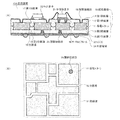
携帯電話等の電子機器の小型化および高機能化に伴い、その内部に収納される回路装置においては、多層の配線層を具備するものが主流になっている。図15を参照して、多層基板107を有する回路装置を説明する(下記特許文献1)。 As electronic devices such as mobile phones become smaller and more functional, circuit devices housed therein are mainly provided with a multilayer wiring layer. A circuit device having a multilayer substrate 107 will be described with reference to FIG.
ここでは、多層基板107の上面に形成された第1の配線層102Aにパッケージ105等の回路素子が実装されることで回路装置が構成されている。 Here, a circuit device is configured by mounting circuit elements such as a package 105 on the first wiring layer 102 </ b> A formed on the upper surface of the multilayer substrate 107.
多層基板107は、ガラスエポキシ等の樹脂から成る基材101の表面及び裏面に配線層が形成されている。ここでは、基材101の上面に第1の配線層102Aおよび第2の配線層102Bが形成されている。第1の配線層102Aと第2の配線層102Bとは、絶縁層103を介して積層されている。基材101の下面には、第3の配線層102Cおよび第4の配線層102Dが、絶縁層103を介して積層されている。また、各配線層は、絶縁層103を貫通して設けられた接続部104により所定の箇所にて接続されている。 In the multilayer substrate 107, wiring layers are formed on the front surface and the back surface of the base material 101 made of a resin such as glass epoxy. Here, the first wiring layer 102 </ b> A and the second wiring layer 102 </ b> B are formed on the upper surface of the substrate 101. The first wiring layer 102A and the second wiring layer 102B are stacked with an insulating layer 103 interposed therebetween. A third wiring layer 102 </ b> C and a fourth wiring layer 102 </ b> D are stacked on the lower surface of the substrate 101 with an insulating layer 103 interposed therebetween. Each wiring layer is connected at a predetermined location by a connecting portion 104 provided through the insulating layer 103.
最上層の第1の配線層102Aには、パッケージ105が固着されている。ここでは、半導体素子105Aが樹脂封止されたパッケージ105が、半田等から成る接続電極106を介して面実装されている。多層基板107の表面には、パッケージ105の他にも、チップコンデンサやチップ抵抗等の受動素子や、ベアの半導体素子等が実装されても良い。ここで、多層基板107の厚みは、例えば1mm程度である。 A package 105 is fixed to the uppermost first wiring layer 102A. Here, the package 105 in which the semiconductor element 105A is resin-sealed is surface-mounted via a connection electrode 106 made of solder or the like. In addition to the package 105, passive elements such as chip capacitors and chip resistors, bare semiconductor elements, and the like may be mounted on the surface of the multilayer substrate 107. Here, the thickness of the multilayer substrate 107 is, for example, about 1 mm.
上記した構成の多層基板107の製造方法は次の通りである。先ず、エポキシ樹脂等の樹脂系の材料から成る基材101の上面及び下面に第2の配線層102Bおよび第3の配線層102Cを形成する。これらの配線層は、貼着された導電膜のエッチングまたは選択的なメッキ処理により形成される。次に、第2の配線層102Bおよび第3の配線層102Cを、樹脂から成る絶縁層103により被覆する。更に、絶縁層103の表面に第1の配線層102Aおよび第4の配線層102Dを形成する。これらの配線層の形成方法は、上記した第2の配線層102B等と同様である。更に、絶縁層103を貫通して第1の配線層102Aと第2の配線層102Bとを接続する接続部104を形成する。
しかしながら、上述した構成の多層基板(配線基板)を有する回路装置では、多層基板107のコア層である基材101が、ガラスエポキシ樹脂等の樹脂材料から成るものであったため、熱伝導率が低く、基板を経由した放熱を良好に行えない問題があった。 However, in the circuit device having the multilayer substrate (wiring substrate) having the above-described configuration, since the base material 101 which is the core layer of the multilayer substrate 107 is made of a resin material such as glass epoxy resin, the thermal conductivity is low. There was a problem that heat dissipation via the substrate could not be performed satisfactorily.
また、基材101の材料として金属を採用する構造もあるが、通常は、1枚の金属板の如き状態のコア基材が用いられるため、このコア基材の電位を例えば接地電位に固定すると、局所的にコア基材の電位を変化させることが困難な問題があった。更に、基材101の材料を金属とすると、導電材料である基材101の外周端部が、多層基板107の側面から外部に露出する。従って、金属から成る基材101を外部と絶縁させることが困難になる問題があった。 In addition, there is a structure in which metal is used as the material of the base material 101. However, since a core base material in a state like a single metal plate is usually used, when the potential of the core base material is fixed to, for example, a ground potential. There is a problem that it is difficult to locally change the potential of the core substrate. Furthermore, when the material of the base material 101 is a metal, the outer peripheral end portion of the base material 101 which is a conductive material is exposed to the outside from the side surface of the multilayer substrate 107. Accordingly, there is a problem that it is difficult to insulate the base material 101 made of metal from the outside.
更に、製法上に於いては、樹脂から成る基材101を採用していたので、製造工程の途中段階に於いて基材101にクラックが発生して多層基板107が不良となる問題があった。具体的には、多層基板101の機械的強度を向上させるために、更には、基板全体の放熱性を向上させるために、基材101はアルミナ等のフィラーが高充填された樹脂から成る。このことから、基材101が脆くなり、搬送の工程や、多層基板107に素子を差し込み実装する工程等に於いて、基材101にクラックが多発していた。 Further, since the base material 101 made of resin is used in the manufacturing method, there is a problem that a crack occurs in the base material 101 in the middle of the manufacturing process and the multilayer substrate 107 becomes defective. . Specifically, in order to improve the mechanical strength of the multilayer substrate 101, and further to improve the heat dissipation of the entire substrate, the base material 101 is made of a resin highly filled with a filler such as alumina. For this reason, the base material 101 becomes fragile, and cracks frequently occur in the base material 101 in the transporting process, the process of inserting and mounting elements on the multilayer substrate 107, and the like.
また、基材101の材料として金属を採用する方法もあるが、この場合は、基材の上面に積層される配線層と、基材の下面に積層される配線層とを効率的に導通させる製造方法が確立されていなかった。 There is also a method of using metal as the material of the base material 101. In this case, the wiring layer laminated on the upper surface of the base material and the wiring layer laminated on the lower surface of the base material are efficiently conducted. The manufacturing method has not been established.
本発明は上記問題点を鑑みて成されたものであり、その主な目的は、内層の金属コア層の外部との絶縁性が向上された回路装置および配線基板を提供することにある。更に、本発明の目的は、金属から成るコア層を備えた配線基板と回路装置の効率的な製造方法を提供することにある。 The present invention has been made in view of the above-mentioned problems, and a main object thereof is to provide a circuit device and a wiring board with improved insulation from the outside of the inner metal core layer. It is another object of the present invention to provide an efficient manufacturing method of a circuit board and a circuit board having a core layer made of metal.
本発明の回路装置は、配線基板と、前記配線基板に実装された回路素子とを具備し、前記配線基板は、金属コア層と、前記金属コア層の上面および下面を被覆する絶縁層と、前記絶縁層の上面および下面に形成された第1配線層および第2配線層とを有し、前記金属コア層は、分離溝により互いに離間された導電パターンから成り、前記分離溝に前記絶縁層が充填されることで前記導電パターン同士は電気的に絶縁されることを特徴とする。 The circuit device of the present invention comprises a wiring board and a circuit element mounted on the wiring board, and the wiring board includes a metal core layer, an insulating layer covering the upper surface and the lower surface of the metal core layer, A first wiring layer and a second wiring layer formed on an upper surface and a lower surface of the insulating layer, wherein the metal core layer is formed of a conductive pattern separated from each other by a separation groove; The conductive patterns are electrically insulated from each other by being filled.
更に、本発明の回路装置は、配線基板と、前記配線基板に実装された回路素子とを具備し、前記配線基板は、金属コア層と、前記金属コア層の上面および下面を被覆する絶縁層と、前記絶縁層の上面および下面に形成された第1配線層および第2配線層とを有し、前記金属コア層の外周端部は、前記絶縁層から成る前記配線基板の外周端部から離間した内側に位置することを特徴とする。 Furthermore, the circuit device of the present invention includes a wiring board and a circuit element mounted on the wiring board, and the wiring board includes a metal core layer and an insulating layer that covers an upper surface and a lower surface of the metal core layer. And a first wiring layer and a second wiring layer formed on an upper surface and a lower surface of the insulating layer, and an outer peripheral end portion of the metal core layer is an outer peripheral end portion of the wiring substrate made of the insulating layer. It is characterized by being located inside the space.
本発明の回路装置の製造方法は、導電箔の一主面を部分的に除去して導電箔よりも浅い分離溝を形成する第1工程と、前記分離溝が充填されるように前記導電箔の前記一主面を第1絶縁層で被覆する第2工程と、前記分離溝に充填された前記第1絶縁層が露出するまで前記導電箔を他主面から除去して、前記分離溝が設けられた箇所で前記導電箔を分離して導電パターンを形成する第3工程と、前記導電パターンが被覆されるように第2絶縁層を形成する第4工程と、前記第1絶縁層および前記第2絶縁層の主面に、第1配線層および第2配線層を形成する第5工程と、前記第1配線層に回路素子を電気的に接続する第6工程とを具備することを特徴とする。 The method for manufacturing a circuit device of the present invention includes a first step of partially removing one main surface of a conductive foil to form a separation groove shallower than the conductive foil, and the conductive foil so that the separation groove is filled. A second step of covering the one main surface with a first insulating layer; removing the conductive foil from the other main surface until the first insulating layer filled in the separation groove is exposed; A third step of separating the conductive foil at the provided location to form a conductive pattern; a fourth step of forming a second insulating layer so as to cover the conductive pattern; the first insulating layer; A fifth step of forming a first wiring layer and a second wiring layer on the main surface of the second insulating layer, and a sixth step of electrically connecting a circuit element to the first wiring layer are provided. And
更に、本発明の回路装置の製造方法は、導電箔の一主面を部分的に除去して導電箔よりも浅い接続孔を形成する第1工程と、前記接続孔が充填されるように前記導電箔の前記一主面を第1絶縁層で被覆する第2工程と、前記接続孔に充填された前記第1絶縁層が露出するまで前記導電箔を他主面から除去する第3工程と、前記導電箔の他主面および前記接続孔から露出する前記第1絶縁層が被覆されるように第2絶縁層を形成する第4工程と、前記接続孔に対応する箇所の前記第1絶縁層および前記第2絶縁層を貫通する貫通孔を形成する第5工程と、前記第1絶縁層および前記第2絶縁層の主面に、第1配線層および第2配線層を形成して、前記第1配線層と前記第2配線層とを接続する貫通接続部を前記貫通孔の内部に形成する第6工程と、前記第1配線層に回路素子を電気的に接続する第7工程とを具備することを特徴とする。 Furthermore, the method for manufacturing a circuit device according to the present invention includes a first step of partially removing one main surface of the conductive foil to form a connection hole shallower than the conductive foil, and the connection hole filled with the connection hole. A second step of covering the one main surface of the conductive foil with a first insulating layer; a third step of removing the conductive foil from the other main surface until the first insulating layer filled in the connection hole is exposed; A fourth step of forming a second insulating layer so as to cover the other main surface of the conductive foil and the first insulating layer exposed from the connection hole, and the first insulation at a position corresponding to the connection hole. A fifth step of forming a through hole penetrating the layer and the second insulating layer, and forming a first wiring layer and a second wiring layer on a main surface of the first insulating layer and the second insulating layer, A sixth step of forming a through connection portion for connecting the first wiring layer and the second wiring layer inside the through hole. , Characterized by comprising a seventh step of electrically connecting circuit elements to said first wiring layer.
本発明の配線基板は、金属コア層と、前記金属コア層の上面および下面を被覆する絶縁層と、前記絶縁層の上面および下面に形成された第1配線層および第2配線層とを有し、前記金属コア層は、分離溝により互いに離間された導電パターンから成り、前記分離溝に前記絶縁層が充填されることで前記導電パターン同士は電気的に絶縁されることを特徴とする。 The wiring board of the present invention includes a metal core layer, an insulating layer covering the upper surface and the lower surface of the metal core layer, and a first wiring layer and a second wiring layer formed on the upper surface and the lower surface of the insulating layer. The metal core layer includes conductive patterns separated from each other by a separation groove, and the conductive patterns are electrically insulated from each other by filling the separation groove with the insulating layer.
更に、本発明の配線基板は、金属コア層と、前記金属コア層の上面および下面を被覆する絶縁層と、前記絶縁層の上面および下面に形成された第1配線層および第2配線層とを有し、前記金属コア層の外周端部は、前記絶縁層から成る外周端部から離間した内側に位置することを特徴とする。 Furthermore, the wiring board of the present invention includes a metal core layer, an insulating layer covering the upper surface and the lower surface of the metal core layer, a first wiring layer and a second wiring layer formed on the upper surface and the lower surface of the insulating layer, The outer peripheral end of the metal core layer is located inside the outer peripheral end made of the insulating layer.
本発明の配線基板の製造方法は、導電箔の一主面を部分的に除去して導電箔よりも浅い分離溝を形成する第1工程と、前記分離溝が充填されるように前記導電箔の前記一主面を第1絶縁層で被覆する第2工程と、前記分離溝に充填された前記第1絶縁層が露出するまで前記導電箔を他主面から除去して、前記分離溝が設けられた箇所で前記導電箔を分離して導電パターンを形成する第3工程と、前記導電パターンが被覆されるように第2絶縁層を形成する第4工程と、前記第1絶縁層および前記第2絶縁層の主面に、第1配線層および第2配線層を形成する第5工程とを具備することを特徴とする。 The method for manufacturing a wiring board of the present invention includes a first step of partially removing one main surface of a conductive foil to form a separation groove shallower than the conductive foil, and the conductive foil so that the separation groove is filled. A second step of covering the one main surface with a first insulating layer; removing the conductive foil from the other main surface until the first insulating layer filled in the separation groove is exposed; A third step of separating the conductive foil at the provided location to form a conductive pattern; a fourth step of forming a second insulating layer so as to cover the conductive pattern; the first insulating layer; And a fifth step of forming a first wiring layer and a second wiring layer on the main surface of the second insulating layer.
更に、本発明の配線基板の製造方法は、導電箔の一主面を部分的に除去して導電箔よりも浅い接続孔を形成する第1工程と、前記接続孔が充填されるように前記導電箔の前記一主面を第1絶縁層で被覆する第2工程と、前記接続孔に充填された前記第1絶縁層が露出するまで前記導電箔を他主面から除去する第3工程と、前記導電箔の他主面および前記接続孔から露出する前記第1絶縁層が被覆されるように第2絶縁層を形成する第4工程と、前記接続孔に対応する箇所の前記第1絶縁層および前記第2絶縁層を貫通する貫通孔を形成する第5工程と、前記第1絶縁層および前記第2絶縁層の主面に、第1配線層および第2配線層を形成して、前記第1配線層と前記第2配線層とを接続する貫通接続部を前記貫通孔の内部に形成する第6工程とを具備する。 Furthermore, the method for manufacturing a wiring board according to the present invention includes a first step of partially removing one main surface of the conductive foil to form a connection hole shallower than the conductive foil, and the connection hole being filled with the connection hole. A second step of covering the one main surface of the conductive foil with a first insulating layer; a third step of removing the conductive foil from the other main surface until the first insulating layer filled in the connection hole is exposed; A fourth step of forming a second insulating layer so as to cover the other main surface of the conductive foil and the first insulating layer exposed from the connection hole, and the first insulation at a position corresponding to the connection hole. A fifth step of forming a through hole penetrating the layer and the second insulating layer, and forming a first wiring layer and a second wiring layer on a main surface of the first insulating layer and the second insulating layer, A sixth step of forming a through connection portion for connecting the first wiring layer and the second wiring layer inside the through hole. Comprising a.
本発明の回路装置および配線基板によれば、分離溝により互いに電気的に絶縁された複数の導電パターンが、金属コア層として配線基板に内蔵されている。従って、金属コア同士の電位を異ならせることが可能となり、更には、導電パターンを配線として用いることもできる。従って、放熱機能以外の機能を金属コア層に持たせることができ、回路装置の多機能化や小型化を実現することができる。 According to the circuit device and the wiring board of the present invention, the plurality of conductive patterns that are electrically insulated from each other by the separation groove are built in the wiring board as the metal core layer. Accordingly, the potentials of the metal cores can be made different, and further, a conductive pattern can be used as the wiring. Therefore, functions other than the heat dissipation function can be provided to the metal core layer, and the multi-function and miniaturization of the circuit device can be realized.
更に、本発明の回路装置および配線基板によれば、金属コア層を、金属コア層を被覆する絶縁層の外周端部よりも内側に位置させている。即ち、金属コア層の外周端部が絶縁層により被覆されており、外部に露出していない。従って、金属コア層と外部とを良好に絶縁させることができる。 Furthermore, according to the circuit device and the wiring board of the present invention, the metal core layer is positioned inside the outer peripheral end of the insulating layer covering the metal core layer. That is, the outer peripheral end of the metal core layer is covered with the insulating layer and is not exposed to the outside. Therefore, the metal core layer can be well insulated from the outside.
本発明の回路装置および配線基板の製造方法に依れば、コア層として機能する導電パターンを容易に形成することができる。具体的には、本発明では、導電箔の一主面に分離溝を設け、第1絶縁層が分離溝に充填されるように導電箔の一主面を第1絶縁層にて被覆し、その後に分離溝が設けられた箇所で導電箔を分離して導電パターンを形成している。従って、コア層として機能する所望の形状の導電パターンを回路装置の内部に容易に形成できる。 According to the circuit device and the method for manufacturing a wiring board of the present invention, a conductive pattern functioning as a core layer can be easily formed. Specifically, in the present invention, a separation groove is provided on one main surface of the conductive foil, and the main surface of the conductive foil is covered with the first insulating layer so that the first insulating layer is filled in the separation groove. Thereafter, the conductive foil is separated at the location where the separation groove is provided, thereby forming a conductive pattern. Therefore, a conductive pattern having a desired shape that functions as a core layer can be easily formed inside the circuit device.
更に、本発明の回路装置および配線基板の製造方法に依れば、コア層として機能する導電箔を厚み方向に貫通する貫通接続部により、配線層同士を容易に接続することができる。具体的には、導電箔を部分的に窪ませて接続孔を設け、この接続孔が充填されるように導電箔の一主面を第1絶縁層により被覆し、接続孔に充填された第1絶縁層が露出するまで導電箔を他主面から除去し、更に、配線層同士を接続する貫通接続部を接続孔の内部に形成している。このことから、コアとなる導電箔を貫通して配線層同士を貫通する貫通接続部を、任意の箇所に容易に形成することができる。 Furthermore, according to the circuit device and the method for manufacturing a wiring board of the present invention, the wiring layers can be easily connected to each other by the through connection portion that penetrates the conductive foil functioning as the core layer in the thickness direction. Specifically, the conductive foil is partially recessed to provide a connection hole, one main surface of the conductive foil is covered with the first insulating layer so that the connection hole is filled, and the connection hole is filled. The conductive foil is removed from the other main surface until one insulating layer is exposed, and a through connection portion for connecting the wiring layers is formed inside the connection hole. From this, the penetration connection part which penetrates the electrically conductive foil used as a core and penetrates wiring layers can be easily formed in arbitrary places.
<第1の実施の形態>
本形態では、図1から図8を参照して、本形態の回路装置の構成を説明する。
<First Embodiment>
In the present embodiment, the configuration of the circuit device of the present embodiment will be described with reference to FIGS.
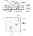
図1を参照して、回路装置10Aの構成を説明する。図1(A)は回路装置10Aの断面図であり、図1(B)は回路装置10Aに内蔵される導電パターン11を示す平面図である。 The configuration of the circuit device 10A will be described with reference to FIG. 1A is a cross-sectional view of the circuit device 10A, and FIG. 1B is a plan view showing a conductive pattern 11 built in the circuit device 10A.
図1(A)を参照して、回路装置10Aは、金属コア層を有する配線基板50の上面に半導体素子21等の回路素子が実装されて構成されている。更に、配線基板50は、金属コア層として機能する導電パターン11と、第1絶縁層12を介して導電パターン11の上面に積層された第1配線層14と、第2絶縁層13を介して導電パターン11の下面に積層された第2配線層15とを主要に具備している。そして、配線基板50の第1配線層14に半導体素子21等の回路素子が実装されている。 Referring to FIG. 1A, circuit device 10A is configured by mounting circuit elements such as semiconductor element 21 on the upper surface of wiring board 50 having a metal core layer. Further, the wiring substrate 50 includes a conductive pattern 11 functioning as a metal core layer, a first wiring layer 14 stacked on the upper surface of the conductive pattern 11 via the first insulating layer 12, and a second insulating layer 13. The second wiring layer 15 is mainly provided on the lower surface of the conductive pattern 11. A circuit element such as the semiconductor element 21 is mounted on the first wiring layer 14 of the wiring board 50.
導電パターン11は、配線基板50全体の機械的強度を担い且つ放熱性を向上させる金属コア層として機能している。従って、導電パターン11は、他の配線層よりも厚く形成され、その厚みは例えば100μm〜200μm程度である。導電パターン11の材料としては、銅を主材料とする金属、アルミニウムを主材料とする金属、合金等を採用することができる。また、導電パターン11の材料として、圧延された銅箔等の圧延金属を採用すると、導電パターン11の機械的強度や放熱性を更に向上させることができる。圧延金属は、メッキ膜と比較すると熱伝導率が数%程度優れている。 The conductive pattern 11 functions as a metal core layer that bears the mechanical strength of the entire wiring board 50 and improves heat dissipation. Therefore, the conductive pattern 11 is formed thicker than the other wiring layers, and the thickness is, for example, about 100 μm to 200 μm. As the material of the conductive pattern 11, a metal mainly made of copper, a metal mainly made of aluminum, an alloy, or the like can be adopted. Further, when a rolled metal such as a rolled copper foil is employed as the material of the conductive pattern 11, the mechanical strength and heat dissipation of the conductive pattern 11 can be further improved. The rolled metal has an excellent thermal conductivity of several percent compared to the plated film.
導電パターン11同士は、第1分離溝17および第2分離溝18から成る分離溝16により所定の間隔で離間されている。分離溝16の幅は例えば100μm〜150μm程度である。ここで、第1分離溝17は導電パターン11の材料である導電箔を上面から選択的にハーフエッチングすることにより設けられ、第2分離溝18はこの導電箔の裏面を選択的にエッチングすることにより設けられる。また、第1分離溝17には、導電パターン11の上面を被覆する第1絶縁層12が充填され、第2分離溝18には導電パターン11の下面を被覆する第2絶縁層13が充填される。 The conductive patterns 11 are separated from each other at a predetermined interval by a separation groove 16 including a first separation groove 17 and a second separation groove 18. The width of the separation groove 16 is, for example, about 100 μm to 150 μm. Here, the first separation groove 17 is provided by selectively half-etching the conductive foil as the material of the conductive pattern 11 from the upper surface, and the second separation groove 18 is formed by selectively etching the back surface of the conductive foil. Is provided. The first separation groove 17 is filled with the first insulating layer 12 covering the upper surface of the conductive pattern 11, and the second separation groove 18 is filled with the second insulating layer 13 covering the lower surface of the conductive pattern 11. The
ここで、第1分離溝17および第2分離溝18の側面は湾曲形状となっており、内部に充填される絶縁層との密着強度が向上されている。また、等方性で進行するウェットエッチングにより形成される第1分離溝17および第2分離溝18により、分離溝16が構成されることで、分離溝16の中央部付近は括れた構成(導電パターン11の側面が外側に突出する構成)となる。このことによっても、第1絶縁層12および第2絶縁層13と導電パターン11との密着強度が向上されている。 Here, the side surfaces of the first separation groove 17 and the second separation groove 18 are curved, and the adhesion strength with the insulating layer filled therein is improved. In addition, the first separation groove 17 and the second separation groove 18 formed by isotropically proceeding wet etching constitute the separation groove 16 so that the vicinity of the central portion of the separation groove 16 is constricted (conductivity). The side surface of the pattern 11 protrudes outward). Also by this, the adhesion strength between the first insulating layer 12 and the second insulating layer 13 and the conductive pattern 11 is improved.
第1絶縁層12および第2絶縁層13は、導電パターン11の上面および下面を被覆している。また、第1絶縁層12は第1分離溝17に充填され、第2絶縁層13は第2分離溝18に充填されている。第1絶縁層12および第2絶縁層13が導電パターン11を被覆する厚みは、例えば50μm〜100μm程度である。更に、第1絶縁層12および第2絶縁層13の材料としては、エポキシ樹脂等の熱硬化性樹脂や、ポリエチレン樹脂等の熱可塑性樹脂を採用することができる。 The first insulating layer 12 and the second insulating layer 13 cover the upper and lower surfaces of the conductive pattern 11. The first insulating layer 12 is filled in the first separation groove 17, and the second insulation layer 13 is filled in the second separation groove 18. The thickness with which the first insulating layer 12 and the second insulating layer 13 cover the conductive pattern 11 is, for example, about 50 μm to 100 μm. Furthermore, as a material for the first insulating layer 12 and the second insulating layer 13, a thermosetting resin such as an epoxy resin or a thermoplastic resin such as a polyethylene resin can be employed.
更に、繊維状または粒子状のフィラーが充填された樹脂材料を第1絶縁層12および第2絶縁層13の材料として採用すると、これらの樹脂層の熱抵抗が低減されて、配線基板50の放熱性を向上させることができる。フィラーの材料としてはシリコン酸化物やシリコン窒化物を採用することができる。また、これらのフィラーが第1絶縁層12および第2絶縁層13に混入されることにより、絶縁層の熱膨張係数が導電パターン11等の導電材料に接近して、温度変化が作用した際の配線基板50の反りが抑制される。 Furthermore, when a resin material filled with fibrous or particulate filler is adopted as the material of the first insulating layer 12 and the second insulating layer 13, the thermal resistance of these resin layers is reduced, and the heat dissipation of the wiring board 50 is achieved. Can be improved. Silicon oxide or silicon nitride can be used as the filler material. In addition, when these fillers are mixed into the first insulating layer 12 and the second insulating layer 13, the thermal expansion coefficient of the insulating layer approaches the conductive material such as the conductive pattern 11, and a temperature change occurs. Warpage of the wiring board 50 is suppressed.
第1配線層14は、第1絶縁層12の上面に形成された配線層であり、第1絶縁層12に貼着された導電膜またはメッキ膜を選択的にエッチングして形成される。薄い導電膜等をエッチングしてパターニングされるため、第1配線層14は微細化が可能であり、その配線幅は20μm〜50μm程度に細くすることができる。また、第1配線層14は、第1絶縁層12を貫通して設けた層間接続部19を経由して、導電パターン11と電気的に接続される。 The first wiring layer 14 is a wiring layer formed on the upper surface of the first insulating layer 12 and is formed by selectively etching a conductive film or a plating film attached to the first insulating layer 12. Since the thin conductive film or the like is patterned by etching, the first wiring layer 14 can be miniaturized, and the wiring width can be reduced to about 20 μm to 50 μm. Further, the first wiring layer 14 is electrically connected to the conductive pattern 11 via an interlayer connection portion 19 provided through the first insulating layer 12.
また、第1配線層14には、チップ素子22や半導体素子21等の回路素子が電気的に接続される。チップ素子22は両端の電極が半田等の導電性の接合材料を介して固着されている。LSIやトランジスタ等である半導体素子21は、導電性または絶縁性の接合剤を介して底面がランド状の第1配線層14に固着され、その上面に設けられた電極は金属細線を介して第1配線層14と接続される。
In addition, circuit elements such as the
第2配線層15は、第2絶縁層13の下面に形成された配線層であり、上記した第1配線層14と同様に、配線幅を20μm〜50μm程度に細くすることができる。また、第2配線層15は、第2絶縁層13を貫通して設けた層間接続部20を介して、導電パターン11の下面と導通している。第2配線層15には、半田等の導電性接着材から成る外部電極を溶着させても良い。 The second wiring layer 15 is a wiring layer formed on the lower surface of the second insulating layer 13, and the wiring width can be reduced to about 20 μm to 50 μm similarly to the first wiring layer 14 described above. In addition, the second wiring layer 15 is electrically connected to the lower surface of the conductive pattern 11 through an interlayer connection portion 20 provided through the second insulating layer 13. An external electrode made of a conductive adhesive such as solder may be welded to the second wiring layer 15.
層間接続部19および層間接続部20は、絶縁層を除去して設けた貫通孔に形成されたメッキ膜等の導電材料から成り、各配線層と導電パターンとを接続する働きを有する。ここでは、第1絶縁層12を貫通して設けた層間接続部19により第1配線層14と導電パターン11とが接続される。また、第2絶縁層13を貫通して設けた層間接続部20により、第2配線層15と導電パターン11とが接続される。ここで、各層間接続部は、電気信号が通過する経路して機能しても良いし、電気信号が通過しない所謂ダミーのものでも良い。層間接続部19が電気信号を通過させないものであっても、層間接続部19を熱が通過するサーマルビアホールとして用いることができる。 The interlayer connection portion 19 and the interlayer connection portion 20 are made of a conductive material such as a plating film formed in a through hole provided by removing the insulating layer, and have a function of connecting each wiring layer and the conductive pattern. Here, the first wiring layer 14 and the conductive pattern 11 are connected by an interlayer connection portion 19 provided through the first insulating layer 12. Further, the second wiring layer 15 and the conductive pattern 11 are connected by the interlayer connection portion 20 provided through the second insulating layer 13. Here, each interlayer connection portion may function as a path through which an electric signal passes, or may be a so-called dummy member through which an electric signal does not pass. Even if the interlayer connection portion 19 does not allow electric signals to pass therethrough, it can be used as a thermal via hole through which heat passes through the interlayer connection portion 19.
上記した第1配線層14と第2配線層15とは、層間接続部19等を経由して導通させることができる。この場合は、第1配線層14→層間接続部19→導電パターン11→層間接続部20→第2配線層15の経路で、両配線層が電気的に接続される。 The first wiring layer 14 and the second wiring layer 15 described above can be conducted through the interlayer connection portion 19 and the like. In this case, both wiring layers are electrically connected through a route of the first wiring layer 14 → the interlayer connection portion 19 → the conductive pattern 11 → the interlayer connection portion 20 → the second wiring layer 15.
ここで、上記した第1配線層14および第2配線層15は、外部と接続される箇所や回路素子が実装される箇所を除いて、ソルダーレジスト(樹脂膜)により被覆されても良い。ここでは、図1(A)を参照して、最下層の第2配線層15は略全面的にソルダーレジスト53により被覆され、部分的にレジスト53が除去されることで、第2配線層15が部分的に露出している。更に、レジスト53から露出する第2配線層15の下面には、半田等から成る外部電極54が溶着されている。更に、レジストから露出する第1配線層14および第2配線層15は、ボンディング性を向上させるために、金メッキ膜により被覆されても良い。 Here, the first wiring layer 14 and the second wiring layer 15 described above may be covered with a solder resist (resin film) except for a portion connected to the outside and a portion where a circuit element is mounted. Here, referring to FIG. 1A, the lowermost second wiring layer 15 is almost entirely covered with a solder resist 53, and the resist 53 is partially removed, so that the second wiring layer 15 is removed. Is partially exposed. Further, an external electrode 54 made of solder or the like is welded to the lower surface of the second wiring layer 15 exposed from the resist 53. Furthermore, the first wiring layer 14 and the second wiring layer 15 exposed from the resist may be covered with a gold plating film in order to improve bonding properties.
更に、第1配線層14、導電パターン11および第2配線層15から成る3層の多層配線が構成されているが、絶縁層を介して更に多層の配線層を積層させることにより、4層以上の配線層を構築しても良い。 Further, a three-layered multilayer wiring composed of the first wiring layer 14, the conductive pattern 11 and the second wiring layer 15 is configured. By stacking a multilayer wiring layer through an insulating layer, four or more layers are formed. The wiring layer may be constructed.
図1(B)に、配線基板50に埋め込まれる導電パターン11の平面的な形状の一例を示す。ここでは、略等間隔の分離溝16により、多数個の導電パターン11が離間されている。換言すると分離溝16に充填された第1絶縁層12および第2絶縁層13により各導電パターン11同士は電気的に分離(絶縁)されている。従って、各導電パターン11を層間接続部19、20を経由して、第1配線層14または第2配線層15と接続することで、各導電パターン11の電位を異ならせることができる。例えば、これらの導電パターン11は、第1配線層14と第2配線層15に入出力される電気信号が通過する信号パターンとして用いられても良いし、所定の箇所にて固定電位(例えば電源電位や接地電位)を取り出すためのパターンとして用いられても良い。 FIG. 1B shows an example of a planar shape of the conductive pattern 11 embedded in the wiring board 50. Here, a large number of conductive patterns 11 are separated by substantially uniform separation grooves 16. In other words, the conductive patterns 11 are electrically separated (insulated) by the first insulating layer 12 and the second insulating layer 13 filled in the separation groove 16. Therefore, by connecting each conductive pattern 11 to the first wiring layer 14 or the second wiring layer 15 via the interlayer connection portions 19 and 20, the potential of each conductive pattern 11 can be made different. For example, these conductive patterns 11 may be used as a signal pattern through which an electric signal input / output to / from the first wiring layer 14 and the second wiring layer 15 passes, or a fixed potential (for example, a power source) at a predetermined location. (Potential or ground potential) may be used as a pattern for extracting.
本形態の回路装置10Aは、半導体素子21やチップ素子22等の多数の回路素子が内蔵されるSIP型のものである。従って、一つの半導体素子が内蔵されるディスクリート型のものと比較すると、本形態の回路装置10Aは、装置全体の発熱量は非常に大きく、より大規模且つ複雑な電気回路が内蔵される。このことから、金属コア層である導電パターン11を互いに分離して電位を異ならせることで、放熱性の向上以外の機能を金属コア層に持たせることが可能となり、装置全体の高機能化および小型化を実現できる。
The circuit device 10A of this embodiment is of the SIP type in which a large number of circuit elements such as the semiconductor element 21 and the
更に、導電パターン11は、上面および下面がサーマルビアとして機能する層間接続部19、層間接続部20を介して各配線層と熱的に結合されて、放熱を向上させるためのパターンとして用いられても良い。ここでは、半導体素子21の下方に複数のサーマルビアホール46が設けられており、半導体素子21はサーマルビアホール46を介して直下の導電パターン11と熱的に結合されている。このことにより、半導体素子21として発熱量が大きいパワー系のトランジスタが採用されても、発生する多量の熱は、サーマルビアホール46および導電パターン11を経由して外部に良好に放出される。 Furthermore, the conductive pattern 11 is thermally coupled to each wiring layer via the interlayer connection portion 19 and the interlayer connection portion 20 whose upper and lower surfaces function as thermal vias, and is used as a pattern for improving heat dissipation. Also good. Here, a plurality of thermal via holes 46 are provided below the semiconductor element 21, and the semiconductor element 21 is thermally coupled to the conductive pattern 11 directly below via the thermal via hole 46. Thus, even if a power transistor having a large calorific value is adopted as the semiconductor element 21, a large amount of generated heat is favorably released to the outside through the thermal via hole 46 and the conductive pattern 11.
更にまた、図1(B)を参照して、金属コア層である導電パターン11の外周端部は、絶縁層51(第1絶縁層12および第2絶縁層13)から離間した内部に位置している。即ち、図1(A)に示すように、導電パターン11の最外周部の側面は、第1絶縁層12および第2絶縁層13から成る絶縁層51により被覆されて、外部に露出していない。このことにより、全ての導電パターン11が絶縁層51により包み込まれて外部に露出しない構造が実現され、導電パターン11を外部から絶縁することができる。 Still further, referring to FIG. 1B, the outer peripheral end of the conductive pattern 11 that is the metal core layer is located inside the insulating layer 51 (the first insulating layer 12 and the second insulating layer 13). ing. That is, as shown in FIG. 1A, the side surface of the outermost peripheral portion of the conductive pattern 11 is covered with the insulating layer 51 including the first insulating layer 12 and the second insulating layer 13 and is not exposed to the outside. . As a result, a structure in which all the conductive patterns 11 are enclosed by the insulating layer 51 and are not exposed to the outside is realized, and the conductive patterns 11 can be insulated from the outside.
また、上記した配線基板50に於いては、各層の残存率(基板全体の面積に対するパターンまたは配線層の面積の比率)は、略一定にした方がよい。例えば、第1配線層14、導電パターン11および第2配線層15の残存率は、80%±10%程度が好ましい。このように各層の残存率を略一定にすることで、ワイヤボンディングの工程等の加熱が伴う工程に於ける、配線基板50の反り上がりを防止することができる。また、金属コア層が図2に示すようにパターニングされていないベタのものである場合は、第1配線層14および第2配線層15の残存率を上記した範囲で略同等にしたらよい。 Further, in the wiring board 50 described above, it is preferable that the remaining ratio of each layer (the ratio of the pattern or the area of the wiring layer to the area of the entire board) is substantially constant. For example, the remaining ratio of the first wiring layer 14, the conductive pattern 11, and the second wiring layer 15 is preferably about 80% ± 10%. Thus, by making the remaining rate of each layer substantially constant, it is possible to prevent the wiring substrate 50 from warping in a process involving heating, such as a wire bonding process. In addition, when the metal core layer is a solid one that is not patterned as shown in FIG. 2, the remaining rates of the first wiring layer 14 and the second wiring layer 15 may be made substantially equal in the above-described range.
更に、基板全体の放熱性を考慮すると、金属材料から成る第1配線層14等の方が、樹脂材料から成る第1絶縁層12等よりも熱伝導率が良いので、第1配線層14等の各層の残存率は高い方がよい。例えば、第1配線層14、導電パターン11および第2配線層15の残存率は、50%以上が好ましく、更に好ましいのは70%以上であり、特に好ましいのは80%以上である。このように第1配線層14等の各層の残存率を大きくすることで、定常熱抵抗を小さくし、半導体素子21等の回路素子から発生する熱を、配線基板50を経由して良好に外部に放出させることができる。ここで、金属コア層が図2に示すようにパターニングされていないベタのものである場合は、第1配線層14および第2配線層15の残存率を上記した範囲で高くしたらよい。 Furthermore, considering the heat dissipation of the entire substrate, the first wiring layer 14 made of a metal material has better thermal conductivity than the first insulating layer 12 made of a resin material, so the first wiring layer 14 etc. The higher the remaining rate of each layer, the better. For example, the remaining ratio of the first wiring layer 14, the conductive pattern 11, and the second wiring layer 15 is preferably 50% or more, more preferably 70% or more, and particularly preferably 80% or more. Thus, by increasing the residual ratio of each layer such as the first wiring layer 14, the steady thermal resistance is reduced, and the heat generated from the circuit elements such as the semiconductor element 21 can be satisfactorily externalized via the wiring substrate 50. Can be released. Here, when the metal core layer is a solid one that is not patterned as shown in FIG. 2, the residual ratio of the first wiring layer 14 and the second wiring layer 15 may be increased within the above-described range.
次に、図2を参照して、他の形態の回路装置10Bの構成を説明する。図2(A)は回路装置10Bの断面図であり、図2(B)は内蔵される導電箔25を示す平面図である。回路装置10Bの基本的な構成は上述した回路装置10Aと同様であり、相違点は貫通接続部23を有している点にある。この相違点を中心に回路装置10Bの構成を説明する。 Next, with reference to FIG. 2, the configuration of another form of circuit device 10B will be described. 2A is a cross-sectional view of the circuit device 10B, and FIG. 2B is a plan view showing the conductive foil 25 incorporated therein. The basic configuration of the circuit device 10 </ b> B is the same as that of the circuit device 10 </ b> A described above, and the difference is that it has a through connection part 23. The configuration of the circuit device 10B will be described focusing on this difference.
図2(A)を参照して、回路装置10Bでは、金属コア層としてパターニングされていないベタの導電箔25を具備している。導電箔25の厚み及び材料は、上述した導電パターン11と同様でよい。導電箔25は、第1配線層14に実装された回路素子に入出力される電気信号が通過しても良いし、所定の箇所にて固定電位(接地電位や電源電位)が層間接続部を介して取り出されても良いし、電気的にフローティングにして放熱の為のみに用いられても良い。このような導電箔25を金属コア層として採用することで、導電箔25により配線基板50全体の機械的強度が向上される。更に、任意の箇所で、層間接続部19、層間接続部20を経由して、導電箔25から所定の電位(接地電位や電源電位)を取り出すことができるので、第1配線層14および第2配線層15を設計する際の自由度を向上させることができる。 Referring to FIG. 2A, the circuit device 10B includes a solid conductive foil 25 that is not patterned as a metal core layer. The thickness and material of the conductive foil 25 may be the same as those of the conductive pattern 11 described above. The conductive foil 25 may pass an electric signal input / output to / from a circuit element mounted on the first wiring layer 14, and a fixed potential (a ground potential or a power supply potential) may pass through the interlayer connection portion at a predetermined location. Or may be used only for heat dissipation by being electrically floating. By adopting such a conductive foil 25 as the metal core layer, the mechanical strength of the entire wiring board 50 is improved by the conductive foil 25. Furthermore, since a predetermined potential (ground potential or power supply potential) can be taken out from the conductive foil 25 via the interlayer connection portion 19 and the interlayer connection portion 20 at an arbitrary place, the first wiring layer 14 and the second wiring layer 14 The degree of freedom in designing the wiring layer 15 can be improved.
導電箔25を部分的に厚み方向に貫通して接続孔42が設けられている。接続孔42は、導電箔25の上面から設けた第1接続孔27と、導電箔25の下面から設けた第2接続孔28とから成る。また、第1接続孔27には第1絶縁層12が充填され、第2接続孔28には第2絶縁層13が充填されている。平面的に円形の形状を呈する接続孔42の径は、例えば、100μm〜200μm程度である。 A connection hole 42 is provided through the conductive foil 25 partially in the thickness direction. The connection hole 42 includes a first connection hole 27 provided from the upper surface of the conductive foil 25 and a second connection hole 28 provided from the lower surface of the conductive foil 25. The first connection hole 27 is filled with the first insulating layer 12, and the second connection hole 28 is filled with the second insulating layer 13. The diameter of the connection hole 42 having a circular shape in plan is, for example, about 100 μm to 200 μm.
図2(A)および図2(B)を参照して、貫通接続部23は、接続孔42の内部に充填された樹脂材料を貫通して設けられ、上層の第1配線層14と下層の第2配線層15とを導通させる働きを有する。具体的には、貫通接続部23は、平面的に貫通孔24の内部に位置する第1絶縁層12および第2絶縁層13が貫通されるように貫通孔を設け、この貫通孔に銅等の導電材料を埋め込むことにより形成される。貫通接続部23の直径は、例えば50μm〜100μm程度である。貫通接続部23を設けることにより、導電箔25を経由せずに第1配線層14と第2配線層15とを電気的に接続させることができる。 Referring to FIGS. 2A and 2B, the through-connection portion 23 is provided through the resin material filled in the connection hole 42, and the upper first wiring layer 14 and the lower layer are connected to each other. The second wiring layer 15 is electrically connected. Specifically, the through-connecting portion 23 is provided with a through-hole so that the first insulating layer 12 and the second insulating layer 13 that are located inside the through-hole 24 in plan view are penetrated, and copper or the like is provided in the through-hole. It is formed by embedding a conductive material. The diameter of the through connection portion 23 is, for example, about 50 μm to 100 μm. By providing the through connection portion 23, the first wiring layer 14 and the second wiring layer 15 can be electrically connected without passing through the conductive foil 25.
図2(B)を参照して、金属コア層である導電箔25の外周端部は、配線基板50の外周端部よりも内側に位置している。即ち、導電箔25の側面は、絶縁層51により被覆されているので、導電箔25は外部と絶縁されており耐圧が充分に確保されている。 Referring to FIG. 2B, the outer peripheral end of conductive foil 25 that is a metal core layer is located inside the outer peripheral end of wiring substrate 50. That is, since the side surface of the conductive foil 25 is covered with the insulating layer 51, the conductive foil 25 is insulated from the outside, and a sufficient withstand voltage is secured.
図3を参照して、更なる他の構成の回路装置10Cを説明する。図3(A)は回路装置10Cの断面図であり、図3(B)は回路装置10Cに内蔵される導電パターン11の平面図である。 A circuit device 10C having still another configuration will be described with reference to FIG. 3A is a cross-sectional view of the circuit device 10C, and FIG. 3B is a plan view of the conductive pattern 11 built in the circuit device 10C.
この図に示す回路装置10Cは、上述した回路装置10Aと回路装置10Bとを組み合わせたものである。即ち、導電パターン11に設けた接続孔42の内部に貫通接続部23が設けられている。この構成により、より複雑な電気回路を回路装置10Cに構成することができる。 The circuit device 10C shown in this figure is a combination of the circuit device 10A and the circuit device 10B described above. That is, the through connection portion 23 is provided inside the connection hole 42 provided in the conductive pattern 11. With this configuration, a more complicated electric circuit can be configured in the circuit device 10C.
図3(A)を参照して、第1配線層14は、第1絶縁層12を貫通する層間接続部19を介して、導電パターン11と電気的または熱的に接続される。同様に、第2配線層15は、第2絶縁層13を貫通する層間接続部20を介して、電気的または熱的に導電パターン11と接続される。 Referring to FIG. 3A, the first wiring layer 14 is electrically or thermally connected to the conductive pattern 11 through an interlayer connection portion 19 that penetrates the first insulating layer 12. Similarly, the second wiring layer 15 is electrically or thermally connected to the conductive pattern 11 via the interlayer connection portion 20 that penetrates the second insulating layer 13.
また、接続孔42が設けられた領域の第1絶縁層12および第2絶縁層13を貫通する貫通接続部23を介して、第1配線層14と第2配線層15が電気的に接続されている。具体的には、図3(B)を参照して、回路装置10Cの右側下側に設けた導電パターン11Aに接続孔42を設け、この接続孔42の内部に貫通接続部23が形成されている。ここで、貫通接続部23は、必ずしも接続孔42の内部に設けられる必要はなく、分離溝16の内部に位置する第1絶縁層12および第2絶縁層13を貫通するように貫通接続部23を設けても良い。 In addition, the first wiring layer 14 and the second wiring layer 15 are electrically connected through the through connection portion 23 that penetrates the first insulating layer 12 and the second insulating layer 13 in the region where the connection hole 42 is provided. ing. Specifically, referring to FIG. 3B, a connection hole 42 is provided in the conductive pattern 11 </ b> A provided on the lower right side of the circuit device 10 </ b> C, and the through-connection portion 23 is formed inside the connection hole 42. Yes. Here, the through-connection portion 23 is not necessarily provided in the connection hole 42, and the through-connection portion 23 penetrates the first insulating layer 12 and the second insulating layer 13 located in the separation groove 16. May be provided.
図4の断面図を参照して、他の構成の回路装置10Dを説明する。回路装置10Dの基本的な構成は上述した回路装置10Aと同様であり、相違点は絶縁層に回路素子が内蔵された点にある。 A circuit device 10D having another configuration will be described with reference to the cross-sectional view of FIG. The basic configuration of the circuit device 10D is the same as that of the circuit device 10A described above, and the difference is that a circuit element is built in the insulating layer.
ここでは、導電パターン11の下面を被覆する第2絶縁層13の内部に内蔵素子26が内蔵されている。ここでは、内蔵素子26はチップコンデンサやチップ抵抗であるチップ型素子であり、半田等の接合材を介して両端の電極が導電パターン11に接続されている。ここで、内蔵素子26としては、チップ型素子の他にも、LIS等の能動素子や受動素子を全般的に採用できる。内蔵素子26は、第2絶縁層13に内蔵されても良いし、第1絶縁層12に内蔵されても良いし、両者に内蔵されても良い。内蔵素子26を採用することで、回路装置10Dの実装密度を向上させることができる。 Here, a built-in element 26 is built in the second insulating layer 13 covering the lower surface of the conductive pattern 11. Here, the built-in element 26 is a chip-type element that is a chip capacitor or a chip resistor, and electrodes at both ends are connected to the conductive pattern 11 via a bonding material such as solder. Here, as the built-in element 26, in addition to the chip-type element, an active element such as LIS or a passive element can be generally employed. The built-in element 26 may be built into the second insulating layer 13, may be built into the first insulating layer 12, or may be built into both. By adopting the built-in element 26, the mounting density of the circuit device 10D can be improved.
図5を参照して、次に、他の構成の回路装置10Eの構造を説明する。図5(A)は回路装置10Eの断面図であり、図5(B)は分離溝16Aの部分を拡大した断面図である。 Next, the structure of the circuit device 10E having another configuration will be described with reference to FIG. 5A is a cross-sectional view of the circuit device 10E, and FIG. 5B is an enlarged cross-sectional view of the separation groove 16A.
図5(A)を参照して、回路装置10Eの基本的な構成は、図1に示した回路装置10Aと基本的には同様であり、相違点は、分離溝16Aを構成する第1分離溝17Aと第2分離溝18Aとの大きさが異なる点になる。 Referring to FIG. 5A, the basic configuration of circuit device 10E is basically the same as that of circuit device 10A shown in FIG. 1, and the difference is the first separation that forms separation groove 16A. The size of the groove 17A and the second separation groove 18A is different.
即ち、図5(A)の左側に示す分離溝16では、上部に設けた第1分離溝17と第2分離溝18の深さや幅は略同一である。このような構成にすることで、例えば分離溝16の幅を150μm程度に狭くすることができる。しかしながら、この構成であると、回路装置10Eを上方から見た場合、分離溝16が設けられた幅が150μmの領域がデッドスペースとなる。即ち、この領域に層間接続部19や層間接続部20を設けることができず、これらの層間接続の設計の自由度が低かった。 That is, in the separation groove 16 shown on the left side of FIG. 5A, the depth and width of the first separation groove 17 and the second separation groove 18 provided in the upper part are substantially the same. With such a configuration, for example, the width of the separation groove 16 can be reduced to about 150 μm. However, with this configuration, when the circuit device 10E is viewed from above, a region where the width of the separation groove 16 is 150 μm is a dead space. That is, the interlayer connection 19 and the interlayer connection 20 cannot be provided in this region, and the degree of freedom in designing these interlayer connections is low.
そこで、この図に示す回路装置10Eでは、分離溝16を構成する第1分離溝17と第2分離溝18の大きさを異ならせて、配線密度を向上させている。即ち、回路装置10Eの中央部付近に設けた分離溝16Aでは、上部の第1分離溝17Aを小さく形成し、下部の第2分離溝18Aを第1分離溝17Aよりも大きく形成している。このことにより、分離溝16Aが専有する面積を小さくして、層間接続部19の設計の自由度を向上させ、更に、第1配線層14のパターンレイアウトの自由度を向上させることができる。 Therefore, in the circuit device 10E shown in this figure, the first and second separation grooves 17 and 18 constituting the separation groove 16 are made different in size to improve the wiring density. That is, in the separation groove 16A provided near the center of the circuit device 10E, the upper first separation groove 17A is formed smaller, and the lower second separation groove 18A is formed larger than the first separation groove 17A. As a result, the area occupied by the isolation trench 16A can be reduced, the degree of freedom in designing the interlayer connection portion 19 can be improved, and the degree of freedom in pattern layout of the first wiring layer 14 can be improved.
図5(B)を参照して、分離溝16Aの構造を詳述する。導電パターン11間に設けられる分離溝16Aは、上部の第1分離溝17Aと下部の第2分離溝18Aから成り、第1分離溝17Aよりも第2分離溝18Aの方が大きな構成となっている。具体的な大きさの一例を述べると、第1分離溝17Aの幅L1は100μmであり、深さL3は例えば50μm程度である。それに対して、第2分離溝18Aの幅L2は300μmであり、深さL4は100μm程度である。 With reference to FIG. 5B, the structure of the separation groove 16A will be described in detail. The separation groove 16A provided between the conductive patterns 11 includes an upper first separation groove 17A and a lower second separation groove 18A, and the second separation groove 18A is larger than the first separation groove 17A. Yes. As an example of a specific size, the width L1 of the first separation groove 17A is 100 μm, and the depth L3 is, for example, about 50 μm. On the other hand, the width L2 of the second separation groove 18A is 300 μm, and the depth L4 is about 100 μm.
上記のように構成することで、上部に位置する第1分離溝17Aの幅を狭くすることができる。例えば、上述した第1分離溝17と第2分離溝18の幅が同一の場合、分離溝16の幅は150μm程度である。それに対して、ここでは、第1分離溝17Aの幅を比較的小さくすることで、分離溝16Aの上端の幅L1は、100μm程度となる。即ち、本形態の構成により、分離溝16Aの上端部の幅が50μm狭くなり、その分だけ層間接続部19が形成可能な導電パターン11上面の有効面積が増大する。図5(B)を参照すると、第2分離溝18Aの上方に対応する導電パターン11の上面に層間接続部19Aが形成されている。 By comprising as mentioned above, the width | variety of 17 A of 1st separation grooves located in the upper part can be narrowed. For example, when the first separation groove 17 and the second separation groove 18 have the same width, the separation groove 16 has a width of about 150 μm. On the other hand, here, by making the width of the first separation groove 17A relatively small, the width L1 of the upper end of the separation groove 16A becomes about 100 μm. That is, according to the configuration of the present embodiment, the width of the upper end portion of the separation groove 16A is reduced by 50 μm, and the effective area of the upper surface of the conductive pattern 11 on which the interlayer connection portion 19 can be formed increases accordingly. Referring to FIG. 5B, an interlayer connection 19A is formed on the upper surface of the conductive pattern 11 corresponding to the upper side of the second separation groove 18A.
このことにより、層間接続部19の設計の自由度が大きくなり、更に、層間接続部19を介して導電パターン11と接続される第1配線層14の設計の自由度も向上する。特に、第1配線層14は、半導体素子21等が実装される配線層であるので、微細なパターンが多数必要になる場合が多い。従って、この分離溝16Aの構成により、第1配線層14の設計の自由度を益すことで、より多機能な半導体素子21を実装することができる。 As a result, the degree of freedom in designing the interlayer connection portion 19 is increased, and the degree of freedom in designing the first wiring layer 14 connected to the conductive pattern 11 via the interlayer connection portion 19 is also improved. In particular, since the first wiring layer 14 is a wiring layer on which the semiconductor element 21 and the like are mounted, many fine patterns are often required. Therefore, the configuration of the separation groove 16A increases the degree of freedom in designing the first wiring layer 14, and thus a more multifunctional semiconductor element 21 can be mounted.
ここで、上記した分離溝16Aは、コア層である導電パターン11同士を電気的に分離するためのものであったが、この構成は、図2(A)に示した接続孔42にも適用可能である。この場合は、第1接続孔27が第2接続孔28よりも小さく形成される。このような構成によっても、層間接続部19の位置的制約を少なくして、更に、第1配線層14の設計の自由度を向上させることができる。 Here, the separation groove 16A described above is for electrically separating the conductive patterns 11 as the core layer, but this configuration is also applied to the connection hole 42 shown in FIG. Is possible. In this case, the first connection hole 27 is formed smaller than the second connection hole 28. Even with such a configuration, it is possible to reduce the positional restriction of the interlayer connection portion 19 and further improve the degree of freedom in designing the first wiring layer 14.
更に、上記説明では、第1分離溝17Aよりも第2分離溝18Aを大きく形成したが、この大小関係を逆にして、第1分離溝17Aを第2分離溝18Aよりも大きく形成しても良い。このことにより、導電パターン11の下面の有効面積が増大し、図5(A)に示す層間接続部20および第2配線層15の設計の自由度が大きくなる。 Furthermore, in the above description, the second separation groove 18A is formed larger than the first separation groove 17A. However, even if the size relationship is reversed, the first separation groove 17A may be formed larger than the second separation groove 18A. good. This increases the effective area of the lower surface of the conductive pattern 11 and increases the degree of freedom in designing the interlayer connection portion 20 and the second wiring layer 15 shown in FIG.
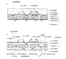
図6を参照して、次に、他の形態の回路装置10Fの構成を説明する。図6(A)は回路装置10Fの断面図であり、図6(B)は回路装置10Fの配線基板50に内蔵される導電パターン11の断面図である。回路装置10Fの基本的な構成は上述した回路装置10Aと同様であり、相違点は、導電パターン11の一部から成る配線47A、47Bが設けられた点にある。 Next, the configuration of another form of circuit device 10F will be described with reference to FIG. 6A is a cross-sectional view of the circuit device 10F, and FIG. 6B is a cross-sectional view of the conductive pattern 11 built in the wiring board 50 of the circuit device 10F. The basic configuration of the circuit device 10F is the same as that of the circuit device 10A described above, and the difference is that wirings 47A and 47B made of a part of the conductive pattern 11 are provided.
図6(A)を参照して、配線47A、47Bは、導電パターン11の一部から成り、他の導電パターン11よりも薄く且つ幅が狭い構成となっている。具体的には、導電パターン11を分離するエッチングの工程にて、分離溝の大きさおよび位置を調節することで配線47A、47Bは形成される。 With reference to FIG. 6A, the wirings 47 </ b> A and 47 </ b> B are composed of a part of the conductive pattern 11, and are thinner and narrower than the other conductive patterns 11. Specifically, the wirings 47A and 47B are formed by adjusting the size and position of the separation groove in the etching process for separating the conductive pattern 11.
先ず、図にて左側に位置する配線47Aは、上方に幅広の第1分離溝17Bを設け、この第1分離溝17Bに接触するように下方から2つの第2分離溝18B、18Cを設けることで、形成される。このことにより、下面が他の導電パターン11の下面と同一平面上に位置し、上面が他の導電パターンの上面よりも下方に位置する配線47Aが得られる。具体的には、例えば、第1分離溝17Bの幅が500μmであり、その下方の両端に幅が150μmの第2分離溝18B、18Cを設けると、幅が200μmの配線47Aが得られる。また、配線47Aの厚みは、導電パターン11の半分程度であり、例えば50μm〜100μm程度である。 First, the wiring 47A located on the left side in the drawing is provided with a wide first separation groove 17B on the upper side, and two second separation grooves 18B and 18C from below so as to be in contact with the first separation groove 17B. And formed. As a result, a wiring 47A is obtained in which the lower surface is located on the same plane as the lower surfaces of the other conductive patterns 11, and the upper surface is located below the upper surfaces of the other conductive patterns. Specifically, for example, when the second separation grooves 18B and 18C having a width of 500 μm and a width of 150 μm are provided at both ends below the first separation groove 17B, a wiring 47A having a width of 200 μm is obtained. Moreover, the thickness of the wiring 47A is about half of the conductive pattern 11, for example, about 50 μm to 100 μm.
更に、幅広の第1分離溝17Bは他の分離溝よりも深くエッチングされるので、パターン分離の為に第2分離溝18B、18Cに要求される深さが浅くなり、その分だけ第2分離溝18B、18Cの幅を狭くすることができる。例えば、第1分離溝17Bの深さは、導電パターン11(材料となる導電箔)の厚みの半分以上とされる。従って、第2分離溝18B、18Cの幅を例えば100μm程度にすることが可能となり、配線47Aと他の導電パターン11とを接近させることができ、パターンの密度を向上させることができる。 Furthermore, since the wide first separation groove 17B is etched deeper than the other separation grooves, the depth required for the second separation grooves 18B and 18C for pattern separation becomes shallower, and the second separation is accordingly made. The width of the grooves 18B and 18C can be reduced. For example, the depth of the first separation groove 17 </ b> B is at least half the thickness of the conductive pattern 11 (conductive foil as a material). Accordingly, the width of the second separation grooves 18B and 18C can be set to about 100 μm, for example, the wiring 47A and the other conductive pattern 11 can be brought close to each other, and the pattern density can be improved.
図にて右側に位置する配線47Bは、下方から幅広の第2分離溝18Dを設け、この第2分離溝18Dに接触する2つの第1分離溝17C、17Dを上方から設けることで形成される。配線47Bの大きさは、上述した配線47Aと同様でよい。配線47Bの上面は、他の導電パターン11の上面と同一平面上に位置し、下面は他の導電パターン11よりも上方に位置している。 The wiring 47B located on the right side in the drawing is formed by providing a wide second separation groove 18D from below and providing two first separation grooves 17C and 17D in contact with the second separation groove 18D from above. . The size of the wiring 47B may be the same as that of the wiring 47A described above. The upper surface of the wiring 47 </ b> B is located on the same plane as the upper surfaces of the other conductive patterns 11, and the lower surface is located above the other conductive patterns 11.
図6(B)を参照して、配線47Aは他の導電パターン11と比較すると細長く延在して、層間接続部20を介して他の配線層と接続される。ここでは、配線47Aは、2つの層間接続部20を経由して、図6(A)に示す第2配線層15と接続される。一方、配線47Bは、2つの層間接続部19を経由して、第1配線層14と接続される。ここで、配線47A、47Bは、一方が層間接続部19を経由して第1配線層14と接続され、他方が層間接続部20を経由して第2配線層15と接続されても良い。 Referring to FIG. 6B, the wiring 47 </ b> A extends longer than the other conductive pattern 11 and is connected to another wiring layer via the interlayer connection portion 20. Here, the wiring 47A is connected to the second wiring layer 15 shown in FIG. On the other hand, the wiring 47B is connected to the first wiring layer 14 via the two interlayer connection portions 19. Here, one of the wirings 47 </ b> A and 47 </ b> B may be connected to the first wiring layer 14 via the interlayer connection portion 19, and the other may be connected to the second wiring layer 15 via the interlayer connection portion 20.
更に、上記した配線47Bと同様に、幅広の第2分離溝18Dが深くエッチングされるので、第1分離溝17C、17Dの幅を狭くすることが可能となり、結果的に配線47Bと他の導電パターン11とを接近させることができる。 Further, similarly to the wiring 47B described above, the wide second separation groove 18D is deeply etched, so that the widths of the first separation grooves 17C and 17D can be reduced. As a result, the wiring 47B and other conductive materials can be reduced. The pattern 11 can be made to approach.
上記したように、配線47A等を設けることで、金属コア層として機能する導電パターン11に、配線を引き回す機能を持たせることが可能となり、より多機能な電気回路を回路装置10Fに内蔵させることができる。 As described above, by providing the wiring 47A and the like, the conductive pattern 11 functioning as the metal core layer can have a function of routing the wiring, and a more multifunctional electric circuit can be built in the circuit device 10F. Can do.
図7を参照して、次に、他の形態の回路装置10Gの構成を説明する。回路装置10Gが上述した回路装置10Aと異なる点は、配線基板50に堀込み部52A、52Bを設けた点にある。 Next, the configuration of another type of circuit device 10G will be described with reference to FIG. The circuit device 10G is different from the circuit device 10A described above in that the wiring substrate 50 is provided with the digging portions 52A and 52B.
堀込み部52Aは、部分的に第1配線層14および第1絶縁層12を除去して設けられており、堀込み部52Aの下面には導電パターン11の上面が露出されている。そして、堀込み部52Aの上面には、半田等の接合材を用いて半導体素子21が実装されている。更に、半導体素子21の上面の電極は、第1配線層14から成り堀込み部52Aの周辺に設けたパッドに、金属細線を用いて電気的に接続される。このように、堀込み部52Aを設けて、導電パターン11の上面に直に半導体素子21を実装することにより、半導体素子21から発生する熱を、導電パターン11を経由して良好に外部に放出させることができる。 The dug portion 52A is provided by partially removing the first wiring layer 14 and the first insulating layer 12, and the upper surface of the conductive pattern 11 is exposed on the lower surface of the dug portion 52A. The semiconductor element 21 is mounted on the upper surface of the dug portion 52A using a bonding material such as solder. Furthermore, the electrode on the upper surface of the semiconductor element 21 is electrically connected to a pad made of the first wiring layer 14 and provided around the engraved portion 52A using a fine metal wire. In this way, by providing the digging portion 52A and mounting the semiconductor element 21 directly on the upper surface of the conductive pattern 11, the heat generated from the semiconductor element 21 is released to the outside through the conductive pattern 11 well. Can be made.
堀込み部52Bは、第2絶縁層13および第2配線層15を部分的に除去して設けられており、その上面からは、半導体素子21が実装された導電パターン11の裏面が露出している。更に、堀込み部52Bの内部に露出する導電パターン11の下面には、半田等から成る外部電極54が溶着されている。このようにすることで、半導体素子21から発生する熱は、樹脂材料を経由することなく、導電パターン11および外部電極54を経由して、良好に外部に放出される。 The dug portion 52B is provided by partially removing the second insulating layer 13 and the second wiring layer 15, and the back surface of the conductive pattern 11 on which the semiconductor element 21 is mounted is exposed from the top surface. Yes. Further, an external electrode 54 made of solder or the like is welded to the lower surface of the conductive pattern 11 exposed inside the dug portion 52B. By doing in this way, the heat generated from the semiconductor element 21 is released to the outside through the conductive pattern 11 and the external electrode 54 without going through the resin material.
図8(A)の断面図を参照して、次に、他の形態の回路装置10Hの構成を説明する。回路装置10Hの構成は、封止樹脂49を具備している点が他の上述した回路装置と異なる。ここでは、チップ素子22、半導体素子21および配線基板50の上面が被覆されるように、封止樹脂49が形成されている。封止樹脂49は、熱可塑性樹脂を用いたインジェクションモールドまたは、熱硬化性樹脂を用いたトランスファーモールドにより形成される。この封止樹脂49の構成は、上述した全ての回路装置に対して適用可能である。
Next, the configuration of another form of the circuit device 10H will be described with reference to the cross-sectional view of FIG. The configuration of the circuit device 10H is different from the other circuit devices described above in that the sealing resin 49 is provided. Here, the sealing resin 49 is formed so that the upper surfaces of the
図8(B)の断面図を参照して、他の形態の回路装置10Iの構成を説明する。回路装置10Iの構成は、上述した回路装置10Fと基本的には同様であり、相違点は配線47A等の構成にある。この相違点を以下に説明する。 With reference to a cross-sectional view of FIG. 8B, the configuration of another form of circuit device 10I will be described. The configuration of the circuit device 10I is basically the same as that of the circuit device 10F described above, and the difference is in the configuration of the wiring 47A and the like. This difference will be described below.
紙面上にて左側に形成される配線47Aの上面には、内蔵素子26が固着されている。ここで、内蔵素子26としては、チップコンデンサやチップ抵抗等が採用される。配線47Aの上面は、第1分離溝17Bの深さに応じて、上面の位置が他の導電パターン11よりも低く形成されている。従って、内蔵素子26を実装することによる配線基板50の厚みの増加が抑制される。 The built-in element 26 is fixed to the upper surface of the wiring 47A formed on the left side on the paper. Here, a chip capacitor, a chip resistor, or the like is employed as the built-in element 26. The upper surface of the wiring 47 </ b> A is formed such that the position of the upper surface is lower than the other conductive patterns 11 in accordance with the depth of the first separation groove 17 </ b> B. Therefore, an increase in the thickness of the wiring board 50 due to the mounting of the built-in element 26 is suppressed.
更に、紙面上の右側には、2つの配線47B、47Cが接近して形成されている。上部に位置している配線47Bは、第1分離溝17C、17Dにより分離されており、第1分離溝17Dは、第1分離溝17Cよりも幅が広く形成されている。更に、下部に位置する配線47Cは、第2分離溝18D、18Eにより分離されており、第2分離溝18Dの方が第2分離溝18Eよりも幅が広く形成されている。 Further, two wirings 47B and 47C are formed close to each other on the right side on the paper surface. The wiring 47B located in the upper part is separated by the first separation grooves 17C and 17D, and the first separation groove 17D is formed wider than the first separation groove 17C. Further, the lower wiring 47C is separated by the second separation grooves 18D and 18E, and the second separation groove 18D is formed wider than the second separation groove 18E.
ここでは、上部の第1分離溝17Dと下部の第2分離溝18Dとを平面的に重畳するように配置することで、配線47Bと配線47Cとを極めて接近させることができる。例えば、配線47Bと配線47Cとが離間する距離D1は、20μm程度まで短くすることができる。このことは、パターンの微細化に大きく寄与する。 Here, by arranging the upper first separation groove 17D and the lower second separation groove 18D so as to overlap each other in a plane, the wiring 47B and the wiring 47C can be made extremely close to each other. For example, the distance D1 between the wiring 47B and the wiring 47C can be shortened to about 20 μm. This greatly contributes to pattern miniaturization.
<第2の実施の形態>
本形態では、図9および図10の断面図を参照して、図1に示した構成の回路装置10Aを製造する方法を説明する。
<Second Embodiment>
In the present embodiment, a method for manufacturing the circuit device 10A having the configuration shown in FIG. 1 will be described with reference to the cross-sectional views of FIGS.
図9(A)を参照して、先ず、導電箔30の表面を部分的にエッチングすることにより第1分離溝17を形成する。導電箔30は、銅またはアルミニウムを主材料とする金属もしくは合金から成り、その厚みは例えば100μm〜200μm程度である。また、導電箔30の材料として、圧延処理が施された圧延金属を採用すると、圧延金属は機械的強度に優れているため、製造工程の途中段階に於いて基板の割れや変形が発生することを抑制することができる。 Referring to FIG. 9A, first, the first separation groove 17 is formed by partially etching the surface of the conductive foil 30. The conductive foil 30 is made of a metal or alloy whose main material is copper or aluminum, and has a thickness of about 100 μm to 200 μm, for example. In addition, when a rolled metal subjected to a rolling process is used as the material of the conductive foil 30, the rolled metal is excellent in mechanical strength, so that cracks and deformation of the substrate occur in the middle of the manufacturing process. Can be suppressed.
ここでは、第1分離溝17が形成される予定の領域を除外した導電箔30の上面をレジスト(不図示)にて被覆した後に、このレジストをエッチングマスクとして用いて導電箔30を上面からエッチングしている。本工程では、塩化鉄または塩化銅を含むエッチャントを用いて、導電箔30をウェットエッチングする。 Here, after covering the upper surface of the conductive foil 30 excluding the region where the first separation groove 17 is to be formed with a resist (not shown), the conductive foil 30 is etched from the upper surface using this resist as an etching mask. doing. In this step, the conductive foil 30 is wet etched using an etchant containing iron chloride or copper chloride.
本工程で形成される第1分離溝17の深さは、導電箔30の厚みの半分程度が好適である。このことにより、等方性に進行するウェットエッチングで形成される第1分離溝17および第2分離溝18により分離溝16を構成でき、分離溝16の幅を分離溝の厚みの半分程度に狭くすることができる(図9(C)参照)。結果的に、配線基板全体に占める導電パターンの面積が増大し、配線基板の機械的強度および放熱特性が向上される。 The depth of the first separation groove 17 formed in this step is preferably about half of the thickness of the conductive foil 30. Accordingly, the separation groove 16 can be constituted by the first separation groove 17 and the second separation groove 18 formed by isotropically proceeding wet etching, and the width of the separation groove 16 is narrowed to about half of the thickness of the separation groove. (See FIG. 9C). As a result, the area of the conductive pattern occupying the entire wiring board increases, and the mechanical strength and heat dissipation characteristics of the wiring board are improved.
例えば、導電箔30の厚みが100μm〜200μmの範囲であれば、第1分離溝17の深さは50μm〜100μm程度でよい。また、本工程のウェットエッチングが等方性に進行することを考慮すると、導電箔30の厚みに応じて、第1分離溝17の幅は50μm〜100μmとなる。 For example, if the thickness of the conductive foil 30 is in the range of 100 μm to 200 μm, the depth of the first separation groove 17 may be about 50 μm to 100 μm. Further, considering that the wet etching in this step proceeds isotropic, the width of the first separation groove 17 is 50 μm to 100 μm depending on the thickness of the conductive foil 30.
上記工程により第1分離溝17が形成された後に、エッチングマスクとして用いた不図示のレジストは導電箔30から剥離されて除去される。 After the first separation groove 17 is formed by the above process, a resist (not shown) used as an etching mask is peeled off from the conductive foil 30 and removed.
図9(B)を参照して、次に、第1分離溝17に充填されるように導電箔30の上面を第1絶縁層12により被覆して、第1絶縁層12の上面に第1導電膜31を貼着する。第1絶縁層12の製造方法としては、半固形状または液状の樹脂材料を導電箔30の上面に塗布した後に加熱硬化しても良いし、フィルム状の樹脂材料を導電箔30の上面に真空プレスで密着させても良い。本工程では、第1分離溝17は導電箔30を貫通せずに厚み方向の途中で終端しているので、液状または半固形状の第1絶縁層12を導電箔30に塗布しても、第1分離溝17からの樹脂材料の漏れ等の問題は発生しない。 Referring to FIG. 9B, next, the upper surface of the conductive foil 30 is covered with the first insulating layer 12 so as to fill the first separation groove 17, and the first insulating layer 12 is covered with the first insulating layer 12. A conductive film 31 is attached. As a manufacturing method of the first insulating layer 12, a semi-solid or liquid resin material may be applied to the upper surface of the conductive foil 30 and then heat-cured, or a film-shaped resin material may be vacuumed on the upper surface of the conductive foil 30. You may make it contact | adhere with a press. In this step, since the first separation groove 17 does not penetrate the conductive foil 30 and terminates in the middle of the thickness direction, even if the liquid or semi-solid first insulating layer 12 is applied to the conductive foil 30, Problems such as leakage of the resin material from the first separation groove 17 do not occur.
第1分離溝17の側面はウェットエッチングにより形成される湾曲面と成っているので、第1絶縁層12は第1分離溝17の側面と嵌合して、両者の密着強度は強固である。 Since the side surface of the first separation groove 17 is a curved surface formed by wet etching, the first insulating layer 12 is fitted to the side surface of the first separation groove 17 and the adhesion strength between the two is strong.
更に、第1絶縁層12の上面は全面的に第1導電膜31により被覆される。ここで、第1導電膜31が貼着された第1絶縁層12を、導電箔30に積層させても良いし、第1絶縁層12が導電箔30に密着された後に、第1導電膜31を第1絶縁層12に貼着しても良い。また、第1導電膜31は、圧延金属から構成しても良いしメッキ法により形成されても良い。第1導電膜31の厚みは、例えば20μm〜50μm程度である。 Further, the upper surface of the first insulating layer 12 is entirely covered with the first conductive film 31. Here, the first insulating layer 12 to which the first conductive film 31 is adhered may be laminated on the conductive foil 30, or after the first insulating layer 12 is in close contact with the conductive foil 30, 31 may be attached to the first insulating layer 12. Moreover, the 1st electrically conductive film 31 may be comprised from a rolled metal, and may be formed by the plating method. The thickness of the first conductive film 31 is, for example, about 20 μm to 50 μm.
第1絶縁層12を構成する樹脂材料としては、熱硬化性樹脂または熱可塑性樹脂の両方が採用可能である。また、繊維状または粒子状のフィラーが混入された樹脂材料を第1絶縁層12として採用しても良い。導電箔30の上面を被覆する第1絶縁層12の厚みは、例えば50μm〜100μm程度である。 As the resin material constituting the first insulating layer 12, both a thermosetting resin or a thermoplastic resin can be employed. Further, a resin material mixed with a fibrous or particulate filler may be adopted as the first insulating layer 12. The thickness of the first insulating layer 12 covering the upper surface of the conductive foil 30 is, for example, about 50 μm to 100 μm.
図9(C)を参照して、次に、導電箔30の裏面から選択的にエッチングして第2分離溝18を形成して、導電箔30を分離して各導電パターン11を得る。具体的な方法は、先ず、第1分離溝17に対応する領域の導電箔30の裏面が露出されるようにレジスト(不図示)を形成する。次に、不図示のレジストから露出する部分の導電箔30の裏面をウェットエッチングして、第2分離溝18を形成する。ここでは、第1分離溝17に充填された第1絶縁層12が露出するまで、ウェットエッチングにより第2分離溝18が形成される。換言すると、第2分離溝18は第1分離溝17に到達するまで形成され、第1分離溝17に充填された第1絶縁層12は、第2分離溝18から露出する。 With reference to FIG. 9C, next, the second separation groove 18 is formed by selectively etching from the back surface of the conductive foil 30, and the conductive foil 30 is separated to obtain each conductive pattern 11. Specifically, first, a resist (not shown) is formed so that the back surface of the conductive foil 30 in a region corresponding to the first separation groove 17 is exposed. Next, the second separation groove 18 is formed by wet-etching the back surface of the portion of the conductive foil 30 exposed from the resist (not shown). Here, the second separation groove 18 is formed by wet etching until the first insulating layer 12 filled in the first separation groove 17 is exposed. In other words, the second separation groove 18 is formed until it reaches the first separation groove 17, and the first insulating layer 12 filled in the first separation groove 17 is exposed from the second separation groove 18.
第2分離溝18の深さは、少なくとも第1分離溝17に充填された第1絶縁層12が露出する深さ以上である必要がある。従って、例えば、導電箔30の厚みが100μm〜200μmであり、第1分離溝17の深さが50μm〜100μmである場合は、第2分離溝18の深さは50μm〜100μm程度である。即ち、第1分離溝17の深さと第2分離溝18の深さとを加算した距離は、導電箔30の厚み以上である必要がある。第1分離溝17に充填された第1絶縁層12を、確実に第2分離溝18から露出させるためには、第1分離溝17の深さと第2分離溝18の深さとを加算した距離は、導電箔30の厚みよりも数十μm程度長い方が好適である。 The depth of the second separation groove 18 needs to be at least greater than the depth at which the first insulating layer 12 filled in the first separation groove 17 is exposed. Therefore, for example, when the thickness of the conductive foil 30 is 100 μm to 200 μm and the depth of the first separation groove 17 is 50 μm to 100 μm, the depth of the second separation groove 18 is about 50 μm to 100 μm. That is, the distance obtained by adding the depth of the first separation groove 17 and the depth of the second separation groove 18 needs to be equal to or greater than the thickness of the conductive foil 30. In order to reliably expose the first insulating layer 12 filled in the first separation groove 17 from the second separation groove 18, a distance obtained by adding the depth of the first separation groove 17 and the depth of the second separation groove 18. Is preferably longer by about several tens of μm than the thickness of the conductive foil 30.
上記工程により、図1(B)に示すような形状の導電パターンが得られる。 Through the above steps, a conductive pattern having a shape as shown in FIG.
ここで、第2分離溝18は必ずしも設けられる必要はない。例えば、本工程でエッチングマスクを用いずに導電箔30を裏面から全面的に除去して、第1分離溝17に充填された第1絶縁層12を下方に露出させても良い。この場合は、第1分離溝17のみによって導電パターン11が分離される。 Here, the second separation groove 18 is not necessarily provided. For example, the conductive foil 30 may be entirely removed from the back surface without using an etching mask in this step, and the first insulating layer 12 filled in the first separation groove 17 may be exposed downward. In this case, the conductive pattern 11 is separated only by the first separation groove 17.
図9(D)を参照して、次に、導電パターン11の裏面を第2絶縁層13により被覆し、第2絶縁層13の表面に第2導電膜32を貼着する。ここでは、導電パターン11の下面が被覆され、更に第2分離溝18が充填されるように第2絶縁層13が形成される。第2絶縁層13の厚み、組成および形成方法は、上述した第1絶縁層12と同様でよい。更に、第2絶縁層13の下面に形成される第2導電膜32の厚み、組成および形成方法も、上述した第1導電膜31と同様でよい。 Next, referring to FIG. 9D, the back surface of the conductive pattern 11 is covered with the second insulating layer 13, and the second conductive film 32 is attached to the surface of the second insulating layer 13. Here, the second insulating layer 13 is formed so that the lower surface of the conductive pattern 11 is covered and the second separation groove 18 is filled. The thickness, composition, and formation method of the second insulating layer 13 may be the same as those of the first insulating layer 12 described above. Furthermore, the thickness, composition, and formation method of the second conductive film 32 formed on the lower surface of the second insulating layer 13 may be the same as those of the first conductive film 31 described above.
図10(A)を参照して、次に、導電パターン11と接続される予定の領域の第1導電膜31および第2導電膜32を部分的に除去する。具体的には、第1導電膜31の上面全域にエッチングマスクとして機能するレジスト45を塗布した後に、露光・現像の処理を行い、導電パターン11と接続される箇所の第1導電膜31の表面を露出させる。更に、ウェットエッチングを行い、レジスト45から露出する第1導電膜31を除去する。同様の工程を、第2導電膜32に対しても行い、第2導電膜32を部分的に除去する。本工程が終了した後に、レジスト45は剥離して除去される。 Referring to FIG. 10A, next, the first conductive film 31 and the second conductive film 32 in a region to be connected to the conductive pattern 11 are partially removed. Specifically, after applying a resist 45 functioning as an etching mask over the entire upper surface of the first conductive film 31, exposure / development processing is performed, and the surface of the first conductive film 31 at a location connected to the conductive pattern 11. To expose. Further, wet etching is performed to remove the first conductive film 31 exposed from the resist 45. A similar process is performed on the second conductive film 32 to partially remove the second conductive film 32. After this step is completed, the resist 45 is peeled off and removed.
図10(B)を参照して、次に、第1導電膜31をマスクとして用いたレーザー処理を行い、第1導電膜31の露出部から露出する第1絶縁層12を除去して、露出孔33を形成する。ここでは、露出孔33の底部から導電パターン11の上面が露出するように、第1導電膜31から露出する第1絶縁層12をレーザーエッチングする。更に、本工程では、第2導電膜32から露出する第2絶縁層13を除去して、底部に導電パターン11が露出する露出孔34を形成する。本工程のレーザー照射により、露出孔33等の底部に蒸発された樹脂材料等の残渣が残存する場合は、デスミア処理を行ってこの残渣を除去する。本工程で形成される露出孔33等の側面は、外側に向かって開口面積が増大する傾斜面である。従って、メッキ処理を行う次工程にて、露出孔33内部に於けるメッキ液の流動が促進され、露出孔33の内壁に容易にメッキ膜が付着できる利点がある。 Referring to FIG. 10B, next, laser processing using the first conductive film 31 as a mask is performed, and the first insulating layer 12 exposed from the exposed portion of the first conductive film 31 is removed and exposed. Hole 33 is formed. Here, the first insulating layer 12 exposed from the first conductive film 31 is laser-etched so that the upper surface of the conductive pattern 11 is exposed from the bottom of the exposed hole 33. Further, in this step, the second insulating layer 13 exposed from the second conductive film 32 is removed to form an exposed hole 34 in which the conductive pattern 11 is exposed at the bottom. If a residue such as an evaporated resin material remains on the bottom of the exposure hole 33 or the like by laser irradiation in this step, desmear treatment is performed to remove the residue. Side surfaces such as the exposure holes 33 formed in this step are inclined surfaces whose opening area increases toward the outside. Therefore, in the next process of performing the plating process, the flow of the plating solution in the exposed hole 33 is promoted, and there is an advantage that the plated film can easily adhere to the inner wall of the exposed hole 33.
図10(C)を参照して、次に、露出孔33の内部に層間接続部19等を形成して、各配線層と導電パターンとを導通させる。層間接続部19は、メッキ法により露出孔33内部に形成される金属膜から構成しても良いし、半田や導電性樹脂ペースト等の導電材料を露出孔33に埋め込んでも良い。メッキ法により層間接続部19が形成される場合は、先ず、無電解メッキ法による薄い金属膜(シード層)を少なくとも露出孔33の内壁に設けた後に、このシード層に電圧を印加して電解メッキ法により厚みが数μm程度の銅から成るメッキ膜を形成する。同様の方法により、第2絶縁層13を貫通する露出孔34の側面に、層間接続部20を設ける。ここで、フィリングメッキを行うと、露出孔33、露出孔34が埋め込まれるようにメッキ膜を生成することができる。 Referring to FIG. 10C, next, an interlayer connection portion 19 or the like is formed inside the exposure hole 33, and each wiring layer is electrically connected to the conductive pattern. The interlayer connection portion 19 may be formed of a metal film formed in the exposed hole 33 by a plating method, or a conductive material such as solder or conductive resin paste may be embedded in the exposed hole 33. When the interlayer connection portion 19 is formed by plating, first, a thin metal film (seed layer) by electroless plating is provided on at least the inner wall of the exposure hole 33, and then a voltage is applied to the seed layer to perform electrolysis. A plating film made of copper having a thickness of about several μm is formed by a plating method. By the same method, the interlayer connection portion 20 is provided on the side surface of the exposure hole 34 that penetrates the second insulating layer 13. Here, when filling plating is performed, a plating film can be generated so that the exposed hole 33 and the exposed hole 34 are embedded.
層間接続部19、20が形成された後に、第1導電膜31および第2導電膜32を選択的にエッチングして、第1配線層14および第2配線層15をパターニングする。第1導電膜31および第2導電膜32の厚みは例えば10μm程度で薄いため、その配線幅は20μm〜50μm程度に微細にすることができる。 After the interlayer connection portions 19 and 20 are formed, the first conductive layer 31 and the second conductive layer 32 are selectively etched to pattern the first wiring layer 14 and the second wiring layer 15. Since the thickness of the first conductive film 31 and the second conductive film 32 is about 10 μm, for example, the wiring width can be reduced to about 20 μm to 50 μm.
なお、ここでは、導電パターン11の上方に第1配線層14が積層され、下方に第2配線層15が積層されて3層の多層配線が実現されているが、絶縁層を介して更に配線層を積層させることにより、4層以上の配線層を実現しても良い。積層される配線層の数を増加させることにより、より大規模な電気回路を配線基板に組み込むことができる。 Here, the first wiring layer 14 is stacked above the conductive pattern 11 and the second wiring layer 15 is stacked below the conductive pattern 11 to realize a three-layer multilayer wiring. Four or more wiring layers may be realized by stacking layers. By increasing the number of wiring layers to be stacked, a larger-scale electric circuit can be incorporated into the wiring board.
上記工程が終了した後は、回路素子の実装や外部との接続が行われる箇所を除いて、第1配線層14および第2配線層15を、樹脂膜から成るソルダーレジストにより被覆しても良い。 After the above steps are completed, the first wiring layer 14 and the second wiring layer 15 may be covered with a solder resist made of a resin film, except for a place where circuit elements are mounted or connected to the outside. .
図10(D)を参照して、次に、第1配線層14に回路素子を実装して電気的に接続する。ここでは、チップ素子22が半田等の接合材を介して第1配線層14に接続される。更に、LSI等である半導体素子21の裏面が接合材を介してランド状の第1配線層14に実装され、表面の電極は金属細線を介して第1配線層14と接続される。
Referring to FIG. 10D, next, circuit elements are mounted on the first wiring layer 14 to be electrically connected. Here, the
更に、第2配線層15が被覆されるようにレジスト53を形成した後に、部分的に第2配線層15が露出されるようにレジスト53を除去し、露出する部分の第2配線層15に半田から成る外部電極54を溶着する。更に、一点鎖線が示された箇所で、各ユニットに配線基板50を分離する。また、半導体素子21等が被覆されるように封止樹脂を配線基板50の上面に形成した後に、上記分離の工程を行っても良い。本工程に於いて、レジスト53から露出する各配線層は、金メッキ膜により被覆されても良い。 Further, after the resist 53 is formed so as to cover the second wiring layer 15, the resist 53 is removed so that the second wiring layer 15 is partially exposed, and the exposed second wiring layer 15 is formed. An external electrode 54 made of solder is welded. Further, the wiring board 50 is separated into each unit at a location where a one-dot chain line is shown. Further, after the sealing resin is formed on the upper surface of the wiring substrate 50 so as to cover the semiconductor element 21 and the like, the separation step may be performed. In this step, each wiring layer exposed from the resist 53 may be covered with a gold plating film.
本工程では、分離溝16が形成された箇所で(即ち、導電パターン11や第1配線層14等が存在しない場所で)、配線基板50を分離しているので、ダイシングソー等の切除手段の摩耗を抑制して、分離を行うことができる。また、銅等の導電材料を分離しないので、分離に伴うバリの発生も抑制される。 In this step, since the wiring board 50 is separated at the position where the separation groove 16 is formed (that is, where the conductive pattern 11 and the first wiring layer 14 are not present), the cutting means such as a dicing saw is used. Abrasion can be suppressed and separation can be performed. Moreover, since the conductive material such as copper is not separated, the generation of burrs associated with the separation is suppressed.
上記工程により、例えば、図1に構成を示す回路装置10Aが製造される。 Through the above process, for example, the circuit device 10A having the configuration shown in FIG. 1 is manufactured.
ここで、上記した製造方法では、膜状の導電膜(第1導電膜31および第2導電膜32)をエッチングすることにより配線層を形成したが、導電膜に替えてメッキ膜を用いることもできる。この場合は、第1導電膜31および第2導電膜32は設けられずに、図10(B)に示す露出孔33等を形成した後に、メッキ法により第1絶縁層12および第2絶縁層13を被覆する金属膜を設ける。その後にこの金属膜を選択的にエッチングして、図10(C)に示す第1配線層14および第2配線層15を形成する。このメッキ膜により配線層を設ける製造方法によると、厚みが5μm〜10μm程度の薄い金属膜をエッチングすることにより配線層を形成するので、幅が40μm程度以下の微細な配線層を構成することができる。 Here, in the manufacturing method described above, the wiring layer is formed by etching the film-like conductive film (the first conductive film 31 and the second conductive film 32), but a plating film may be used instead of the conductive film. it can. In this case, the first conductive layer 31 and the second conductive layer 32 are not provided, and after forming the exposed holes 33 and the like shown in FIG. A metal film covering 13 is provided. Thereafter, the metal film is selectively etched to form the first wiring layer 14 and the second wiring layer 15 shown in FIG. According to the manufacturing method in which the wiring layer is provided by this plating film, the wiring layer is formed by etching a thin metal film having a thickness of about 5 μm to 10 μm, and therefore, a fine wiring layer having a width of about 40 μm or less can be formed. it can.
また、図4に示す回路装置10Dを製造する場合は、第2絶縁層13を形成する前に、内蔵素子26を導電パターン11に実装すればよい。更に、図5に示す回路装置10Eを製造する場合は、上記工程にて、第2分離溝18の幅を第1分離溝17よりも大きくすればよい。 Further, when the circuit device 10 </ b> D shown in FIG. 4 is manufactured, the built-in element 26 may be mounted on the conductive pattern 11 before the second insulating layer 13 is formed. Furthermore, when manufacturing the circuit device 10 </ b> E shown in FIG. 5, the width of the second separation groove 18 may be made larger than that of the first separation groove 17 in the above process.
<第3の実施の形態>
次に、図11および図12の断面図を参照して、図2に構成を示した回路装置10Bの製造方法を説明する。回路装置10Bの製造方法は、基本的には上述した回路装置10Aの製造方法と同様である。両者の相違点は、各絶縁層を貫通する貫通接続部23を形成する点、パターニングされていないベタの導電箔25により金属コアを構成する点にある。この相違点を中心に回路装置10Bの製造方法を説明する。
<Third Embodiment>
Next, a method for manufacturing the circuit device 10B having the configuration shown in FIG. 2 will be described with reference to the cross-sectional views of FIGS. The method for manufacturing the circuit device 10B is basically the same as the method for manufacturing the circuit device 10A described above. The difference between the two is that a through-connecting portion 23 that penetrates each insulating layer is formed, and that a metal core is constituted by a solid conductive foil 25 that is not patterned. A method for manufacturing the circuit device 10B will be described focusing on this difference.
図11(A)を参照して、先ず、導電箔25を上面から部分的にエッチングして、第1接続孔40を設ける。導電箔25の材料としては、厚みが100μm〜200μm程度の金属が採用され、具体的には、銅を主材料とする金属、アルミニウムを主材料とする金属、合金、圧延金属等が採用される。 Referring to FIG. 11A, first, the conductive foil 25 is partially etched from the upper surface to provide the first connection hole 40. As the material of the conductive foil 25, a metal having a thickness of about 100 μm to 200 μm is adopted. Specifically, a metal mainly made of copper, a metal mainly made of aluminum, an alloy, a rolled metal, or the like is adopted. .
第1接続孔40は、導電箔25の上面を選択的にエッチングマスク(不図示)で被覆した後に、エッチングマスクから露出する導電箔25をウェットエッチングすることにより形成される。ここで、第1接続孔40は、導電箔25を貫通して配線層同士を接続する貫通接続部が設けられる箇所に対応して形成される。第1接続孔40の深さは、例えば導電箔25の厚みの半分程度であり、50μm〜100μm程度である。また、等方性に進行するウェットエッチングにより形成される第1接続孔40の幅(直径)は、その深さと同様に、50μm〜100μm程度である。 The first connection hole 40 is formed by wet-etching the conductive foil 25 exposed from the etching mask after selectively covering the upper surface of the conductive foil 25 with an etching mask (not shown). Here, the 1st connection hole 40 is formed corresponding to the location in which the penetration connection part which penetrates the conductive foil 25 and connects wiring layers is provided. The depth of the first connection hole 40 is, for example, about half the thickness of the conductive foil 25 and is about 50 μm to 100 μm. Further, the width (diameter) of the first connection hole 40 formed by wet etching that proceeds isotropically is about 50 μm to 100 μm, similarly to the depth.
図11(B)を参照して、次に、第1接続孔40に充填されるように導電箔25の上面を第1絶縁層12で被覆して、第1絶縁層12の上面に第1導電膜31を貼着する。更に、第1接続孔40に充填された第1絶縁層12が露出されるように、導電箔25を裏面から除去する。ここでは、厚み方向に連続する第1接続孔40および第2接続孔41から接続孔42が構成される。本工程の基本的なプロセスは、上述した第2の実施の形態と同様である。 Referring to FIG. 11B, next, the upper surface of the conductive foil 25 is covered with the first insulating layer 12 so as to fill the first connection holes 40, and the first upper surface of the first insulating layer 12 is covered with the first insulating layer 12. A conductive film 31 is attached. Further, the conductive foil 25 is removed from the back surface so that the first insulating layer 12 filled in the first connection hole 40 is exposed. Here, the connection hole 42 is constituted by the first connection hole 40 and the second connection hole 41 which are continuous in the thickness direction. The basic process of this step is the same as that of the second embodiment described above.
ここでは、第1接続孔40の下方の領域の導電箔25を選択的にウェットエッチングすることにより、第2接続孔41を形成している。第1接続孔40に充填された第1絶縁層12は、第2接続孔41から露出する。ここでも、第1接続孔40に充填された第1絶縁層12を外部に露出させるためには、第1接続孔40の深さと第2接続孔41の深さを加算した長さは、導電箔25の厚みよりも長くなる必要がある。ここで、第2接続孔41を形成するための選択的なエッチングを行わずに、エッチングマスクを使用しない所謂マスクレスなエッチングにより、導電箔25を裏面から全面的に除去して、第1接続孔40に充填された第1絶縁層12を導電箔25の裏面に露出させても良い。 Here, the second connection hole 41 is formed by selectively wet-etching the conductive foil 25 in the region below the first connection hole 40. The first insulating layer 12 filled in the first connection hole 40 is exposed from the second connection hole 41. Also here, in order to expose the first insulating layer 12 filled in the first connection hole 40 to the outside, the length obtained by adding the depth of the first connection hole 40 and the depth of the second connection hole 41 is the conductive length. It needs to be longer than the thickness of the foil 25. Here, the conductive foil 25 is completely removed from the back surface by so-called maskless etching that does not use an etching mask without performing selective etching for forming the second connection hole 41, and the first connection is made. The first insulating layer 12 filled in the holes 40 may be exposed on the back surface of the conductive foil 25.
図11(C)を参照して、次に、第2接続孔41に充填されるように、第2絶縁層13により導電箔25の裏面を被覆して、更に、第2絶縁層13の下面に第2導電膜32を貼着する。この工程の詳細も、上述した第2の実施の形態と同様である。 Referring to FIG. 11C, next, the back surface of the conductive foil 25 is covered with the second insulating layer 13 so that the second connection holes 41 are filled, and the lower surface of the second insulating layer 13 is further covered. The second conductive film 32 is attached to the substrate. The details of this process are also the same as in the second embodiment described above.
図11(D)を参照して、次に、第1導電膜31および第2導電膜32を部分的にエッチングして、露出部43および露出部44を設ける。露出部43は、第1導電膜31または第2導電膜32と、導電パターン11とを接続する層間接続部が形成される箇所に対応して設けられている。更に、露出部44は、接続孔42の上方に位置する第1導電膜31を除去して設けられる。更に、接続孔42の下方にも、第2導電膜32を除去して露出部44が設けられる。露出部43および露出部44を設けることにより、第1導電膜31および第2導電膜32をマスクとしたレーザーエッチングを行い、第1絶縁層12および第2絶縁層13を部分的に除去することができる。 Referring to FIG. 11D, next, the first conductive film 31 and the second conductive film 32 are partially etched to provide an exposed portion 43 and an exposed portion 44. The exposed portion 43 is provided corresponding to a location where an interlayer connection portion that connects the first conductive film 31 or the second conductive film 32 and the conductive pattern 11 is formed. Further, the exposed portion 44 is provided by removing the first conductive film 31 located above the connection hole 42. Further, the exposed portion 44 is also provided below the connection hole 42 by removing the second conductive film 32. By providing the exposed portion 43 and the exposed portion 44, laser etching is performed using the first conductive film 31 and the second conductive film 32 as a mask, and the first insulating layer 12 and the second insulating layer 13 are partially removed. Can do.
図12(A)を参照して、次に、第1導電膜31から露出する第1絶縁層12にレーザーを照射して除去し、露出孔33および貫通孔24を形成する。露出孔33の底部からは導電パターン11の上面を露出させる。また、第2導電膜32から露出する第2絶縁層13をレーザーにて除去して露出孔34を形成し、露出孔34の底部から導電パターン11の下面を露出させる。また、貫通孔24に関しては、一主面からレーザーを照射させることにより、接続孔42に充填された第1絶縁層12および第2絶縁層13を除去して、他主面まで到達させても良い。更には、一主面から照射されるレーザーにより貫通孔24を途中まで形成し、他主面から照射されるレーザーにより残りの部分の貫通孔24を形成しても良い。 Referring to FIG. 12A, next, the first insulating layer 12 exposed from the first conductive film 31 is removed by irradiating a laser to form an exposed hole 33 and a through hole 24. The upper surface of the conductive pattern 11 is exposed from the bottom of the exposure hole 33. Further, the second insulating layer 13 exposed from the second conductive film 32 is removed with a laser to form an exposed hole 34, and the lower surface of the conductive pattern 11 is exposed from the bottom of the exposed hole 34. In addition, with respect to the through hole 24, the first insulating layer 12 and the second insulating layer 13 filled in the connection hole 42 can be removed by irradiating laser from one main surface to reach the other main surface. good. Furthermore, the through-hole 24 may be formed partway with a laser irradiated from one main surface, and the remaining through-hole 24 may be formed with a laser irradiated from the other main surface.
本工程では、接続孔42の内部に充填された第1絶縁層12および第2絶縁層13を貫通する貫通孔24が設けられる。貫通孔24の径は接続孔42よりも細く形成され例えば50μm〜100μm程度である。更に、後に貫通孔24の内部に形成される接続部と導電パターン11とを絶縁させるために、貫通孔24は接続孔42の側壁から離間して設けられている。 In this step, a through hole 24 penetrating the first insulating layer 12 and the second insulating layer 13 filled in the connection hole 42 is provided. The diameter of the through hole 24 is smaller than that of the connection hole 42 and is, for example, about 50 μm to 100 μm. Further, the through hole 24 is provided apart from the side wall of the connection hole 42 in order to insulate the connection portion formed later in the through hole 24 from the conductive pattern 11.
図12(B)を参照して、次に、無電解メッキ法および電解メッキ法により金属膜を形成して、層間接続部19、20および貫通接続部23を形成する。第1絶縁層12を貫通する露出孔33の内部にメッキ膜から成る層間接続部19を形成して、第1導電膜31と導電パターン11とを接続する。また、第2絶縁層13を貫通する露出孔34の内部にメッキ膜から成る層間接続部20を設けて、第2導電膜32と導電パターン11とを接続する。更に、貫通孔24の内部に生成された金属膜により、貫通接続部23が形成される。貫通接続部23により、導電パターン11を挟んで積層された第1導電膜31と第2導電膜32とが、導電箔25を経由せずに電気的に接続される。 Referring to FIG. 12B, next, a metal film is formed by an electroless plating method and an electrolytic plating method, and interlayer connection portions 19 and 20 and through connection portion 23 are formed. An interlayer connection portion 19 made of a plating film is formed in the exposed hole 33 penetrating the first insulating layer 12 to connect the first conductive film 31 and the conductive pattern 11. Further, an interlayer connection portion 20 made of a plating film is provided inside the exposed hole 34 that penetrates the second insulating layer 13 to connect the second conductive film 32 and the conductive pattern 11. Further, the through-connection portion 23 is formed by the metal film generated inside the through-hole 24. The first conductive film 31 and the second conductive film 32 stacked with the conductive pattern 11 interposed therebetween are electrically connected without passing through the conductive foil 25 by the through connection portion 23.
図12(C)を参照して、次に、第1導電膜31および第2導電膜32を選択的にエッチングして、第1配線層14および第2配線層15をパターニングする。ここで、第1配線層14と第2配線層15とは、貫通接続部23を経由して電気的に接続される。 Referring to FIG. 12C, next, the first conductive layer 31 and the second conductive layer 32 are selectively etched, and the first wiring layer 14 and the second wiring layer 15 are patterned. Here, the first wiring layer 14 and the second wiring layer 15 are electrically connected via the through connection portion 23.
図12(D)を参照して、次に、第1配線層14に回路素子を実装する。ここでは、チップ素子22および半導体素子21が第1配線層14に接続される。
Next, referring to FIG. 12D, circuit elements are mounted on the first wiring layer 14. Here, the
以上の工程により、図2に構造を示した回路装置10Bが製造される。ここで、図3に構造を示した回路装置10Cを製造する場合は、分離溝16を製造する工程にて同時に接続孔42が設けられ、層間接続部20を形成する工程と同時に貫通接続部23が設けられる。 Through the above steps, the circuit device 10B having the structure shown in FIG. 2 is manufactured. Here, when the circuit device 10 </ b> C having the structure shown in FIG. 3 is manufactured, the connection hole 42 is provided at the same time in the process of manufacturing the separation groove 16, and the through-connection part 23 is formed at the same time as the process of forming the interlayer connection 20. Is provided.
<第4の実施の形態>
本形態では、図13を参照して、図6に構成を示す回路装置10Fの製造方法を説明する。この製造方法は、基本的には上述した第2の実施の形態と同様であり、相違点は配線47A等を形成するために各分離溝の幅および位置を調節することにある。
<Fourth embodiment>
In this embodiment, a method for manufacturing the circuit device 10F having the configuration shown in FIG. 6 will be described with reference to FIG. This manufacturing method is basically the same as that of the second embodiment described above, and the difference is that the width and position of each separation groove are adjusted in order to form the wiring 47A and the like.
図13(A)を参照して、先ず、ウェットエッチングにより導電箔30の上面から第1分離溝17を形成する。単に後の工程にて導電パターン11を分離するのが目的であれば、第1分離溝17の幅は均一にすればよいが、ここでは、配線を形成するために、幅広の第1分離溝を設けている。具体的には、紙面上にて左側に設けられる第1分離溝17Bの幅は、例えば500μm程度である。それに対して、第1分離溝17C、17Dの幅は、例えば150μm程度である。本工程では、導電箔30の上面を選択的にエッチングマスクで被覆して、ウェットエッチングを行うことで上記第1分離溝17が形成される。 Referring to FIG. 13A, first, first separation grooves 17 are formed from the upper surface of conductive foil 30 by wet etching. If the purpose is simply to separate the conductive pattern 11 in a later step, the width of the first separation groove 17 may be made uniform, but here, in order to form a wiring, the wide first separation groove 17 is formed. Is provided. Specifically, the width of the first separation groove 17B provided on the left side on the paper surface is, for example, about 500 μm. On the other hand, the width of the first separation grooves 17C and 17D is, for example, about 150 μm. In this step, the first separation groove 17 is formed by selectively covering the upper surface of the conductive foil 30 with an etching mask and performing wet etching.
図13(B)を参照して、次に、第1分離溝17B等に充填されるように、導電箔30の上面を第1絶縁層12により被覆して、更に、第1絶縁層12の上面に膜状の第1導電膜31を貼着する。 Referring to FIG. 13B, next, the upper surface of the conductive foil 30 is covered with the first insulating layer 12 so that the first separation grooves 17B and the like are filled. A film-like first conductive film 31 is attached to the upper surface.
図13(C)を参照して、次に、導電箔30を選択的に裏面からウェットエッチングして、各導電パターン11を分離し、更に配線47A等を形成する。先ず、図面にて右端には、第1分離溝17と略同等の幅の第2分離溝18が形成されており、これらの分離溝により、電気的に分離された導電パターン11が得られる。 Referring to FIG. 13C, next, the conductive foil 30 is selectively wet-etched from the back surface to separate the conductive patterns 11 and further form wirings 47A and the like. First, a second separation groove 18 having a width substantially equal to that of the first separation groove 17 is formed at the right end in the drawing, and an electrically isolated conductive pattern 11 is obtained by these separation grooves.
一方、幅広の第1分離溝17Bの下方には、2つの第2分離溝18B、18Cが設けられる。そして、第2分離溝18B、18Cの間に残存する導電箔が配線47Aとなる。第2分離溝18B、18Cの幅は、導電パターン11の分離のために設けられる他の第2分離溝18と同様でよい。具体的には、第1分離溝17Bの幅を500μm、その下方に位置する第2分離溝18B、18Cの幅を150μmとすると、配線47Aの幅は200μm程度である。ここで、第2分離溝18B、18Cは、全ての部分が第1分離溝17Bの下方に位置する必要は無く、第2分離溝18B、18Cの一部が第1分離溝17Bの下方に位置し、他の部分が外側にはみ出ても良い。即ち、第2分離溝18B、18Cと第1分離溝17Bとの断面が接触して、配線47Aが隣接する導電パターン11と分離されてば良い。上記構成の第1分離溝17B等により形成される配線47Aは、その下面が他の導電パターン11の下面と同一平面上に位置し、上面が他の導電パターン11の上面よりも下方に位置している。 On the other hand, two second separation grooves 18B and 18C are provided below the wide first separation groove 17B. The conductive foil remaining between the second separation grooves 18B and 18C becomes the wiring 47A. The widths of the second separation grooves 18 </ b> B and 18 </ b> C may be the same as those of the other second separation grooves 18 provided for separating the conductive pattern 11. Specifically, if the width of the first separation groove 17B is 500 μm and the widths of the second separation grooves 18B and 18C located therebelow are 150 μm, the width of the wiring 47A is about 200 μm. Here, the second separation grooves 18B and 18C do not have to be located all below the first separation groove 17B, and a part of the second separation grooves 18B and 18C is located below the first separation groove 17B. However, other parts may protrude outside. That is, the cross-sections of the second separation grooves 18B and 18C and the first separation groove 17B are in contact with each other, and the wiring 47A is separated from the adjacent conductive pattern 11. The lower surface of the wiring 47A formed by the first separation groove 17B and the like having the above configuration is located on the same plane as the lower surface of the other conductive pattern 11, and the upper surface is located below the upper surface of the other conductive pattern 11. ing.
第1分離溝17C、17Dの下方には、幅が広い第2分離溝18Dが形成される。第2分離溝18Dの幅は、上述した第1分離溝17Bと同様で良く、例えば500μm程度である。第1分離溝17C、17Dおよび第2分離溝18Dで囲まれる部分が、配線47Bである。配線47Bの断面の大きさは上述した配線47Aと同様でよい。配線47Bの上面は、他の導電パターン11の上面と同一平面上に位置し、その下面は他の導電パターン11よりも上方に位置する。 A second separation groove 18D having a large width is formed below the first separation grooves 17C and 17D. The width of the second separation groove 18D may be the same as that of the first separation groove 17B described above, for example, about 500 μm. A portion surrounded by the first separation grooves 17C and 17D and the second separation groove 18D is the wiring 47B. The size of the cross section of the wiring 47B may be the same as that of the wiring 47A described above. The upper surface of the wiring 47B is positioned on the same plane as the upper surfaces of the other conductive patterns 11, and the lower surface thereof is positioned above the other conductive patterns 11.
図13(E)を参照して、次に、層間接続部19、20を設けて、第1配線層14および第2配線層15を形成した後に、半導体素子21等の回路素子を配線基板50に実装して、図6に示す回路装置10Fが製造される。この工程の詳細は、上述した他の実施の形態と同様である。本工程では、層間接続部19、20は、配線47A、47Bが設けられた箇所にも形成されて、これらの配線は第1配線層14または第2配線層15と接続される。 Referring to FIG. 13E, next, after providing interlayer connection portions 19 and 20 to form first wiring layer 14 and second wiring layer 15, circuit elements such as semiconductor element 21 are connected to wiring board 50. The circuit device 10F shown in FIG. 6 is manufactured. The details of this step are the same as in the other embodiments described above. In this step, the interlayer connection portions 19 and 20 are also formed at locations where the wirings 47A and 47B are provided, and these wirings are connected to the first wiring layer 14 or the second wiring layer 15.
<第5の実施の形態>
次に、図14を参照して、図7に構成を示した回路装置10Gの製造方法を説明する。この製造方法は、基本的には上述した第2の実施の形態と同様であり、相違点は堀込み部52A等を設ける点にある。
<Fifth embodiment>
Next, a method for manufacturing the circuit device 10G having the configuration shown in FIG. 7 will be described with reference to FIG. This manufacturing method is basically the same as that of the second embodiment described above, and the difference is that a dug 52A and the like are provided.
図14(A)を参照して、先ず、導電パターン11等が形成された基板を用意する。ここでは、分離溝で分離された導電パターン11の上面および下面が第1絶縁層12および第2絶縁層13により被覆され、第1絶縁層12の上面が第1導電膜31により覆われ、第2絶縁層13の下面が第2導電膜32により被覆される。 Referring to FIG. 14A, first, a substrate on which a conductive pattern 11 and the like are formed is prepared. Here, the upper and lower surfaces of the conductive pattern 11 separated by the separation groove are covered with the first insulating layer 12 and the second insulating layer 13, and the upper surface of the first insulating layer 12 is covered with the first conductive film 31, The lower surface of the two insulating layer 13 is covered with the second conductive film 32.
図14(B)を参照して、次に、堀込み部52Aは、回路素子が実装される予定の部分およびその周辺部に対応する、第1導電膜31および第1絶縁層12を除去して設けられる。具体的な除去方法は、レーザー照射のみにより行われても良いし、エッチング処理とレーザー照射とを組み合わせて行われても良い。第1導電膜31の厚みは数μm程度であるので、出力が大きいレーザーを照射することで、第1導電膜31とその下方の第1絶縁層12を除去することができる。また、エッチングとレーザーとを組み合わせて堀込み部52Aを形成する場合は、先ず、エッチングマスクを用いた選択的なエッチングにより、堀込み部52Aが形成予定の領域の第1導電膜31を除去して第1絶縁層12を露出させる。次に、第1導電膜31から露出する第1絶縁層12をレーザー照射により除去する。いずれの方法によっても、導電パターン11の上面を堀込み部52Aの底面に露出させる。 Referring to FIG. 14B, next, the dug portion 52A removes the first conductive film 31 and the first insulating layer 12 corresponding to the portion where the circuit element is to be mounted and its peripheral portion. Provided. A specific removal method may be performed only by laser irradiation, or may be performed by a combination of etching treatment and laser irradiation. Since the thickness of the first conductive film 31 is about several μm, the first conductive film 31 and the first insulating layer 12 below the first conductive film 31 can be removed by irradiating with a laser having a large output. In the case where the trench 52A is formed by combining etching and laser, first, the first conductive film 31 in the region where the trench 52A is to be formed is removed by selective etching using an etching mask. The first insulating layer 12 is exposed. Next, the first insulating layer 12 exposed from the first conductive film 31 is removed by laser irradiation. In any method, the upper surface of the conductive pattern 11 is exposed on the bottom surface of the engraved portion 52A.
また、堀込み部52Bの形成方法も堀込み部52Aと同様である。この場合は、第2導電膜32およびその上方の第2絶縁層13を部分的に除去して、導電パターン11の下面が露出する堀込み部52Bが設けられる。ここで、堀込み部52Bは、半田等から成る外部電極を導電パターン11の裏面に接触させるために設けられているので、その平面的な大きさは、後に実装される半導体素子21よりも小さくても良い。 The formation method of the dug portion 52B is the same as that of the dug portion 52A. In this case, the second conductive film 32 and the second insulating layer 13 above the second conductive film 32 are partially removed to provide a dug 52B where the lower surface of the conductive pattern 11 is exposed. Here, since the digging portion 52B is provided in order to bring the external electrode made of solder or the like into contact with the back surface of the conductive pattern 11, its planar size is smaller than that of the semiconductor element 21 to be mounted later. May be.
図14(C)を参照して、次に、第1配線層14等を形成した後に回路素子を実装して、回路装置を完成させる。具体的には、第1配線層14および第2配線層15を形成した後に、半導体素子21およびチップ素子22を、第1配線層14に電気的に接続する。本形態では、堀込み部52Aに半導体素子21を収納し、半田等の接合材を介して、半導体素子21を導電パターン11の上面に固着する。そして、堀込み部52Aの周辺部に位置する第1配線層14から成るパッドと、半導体素子21の上面に形成された電極とを、金属細線により電気的に接続する。
Referring to FIG. 14C, next, after forming the first wiring layer 14 and the like, circuit elements are mounted to complete the circuit device. Specifically, after forming the first wiring layer 14 and the second wiring layer 15, the semiconductor element 21 and the
更に、堀込み部52Bから露出する導電パターン11の下面には、半田等から成る外部電極54が溶着される。このように形成することで、半導体素子21は導電パターン11にダイレクトに固着される。従って、半導体素子21から発生した熱は、導電パターン11および外部電極54を経由して良好に外部に放出される。 Further, an external electrode 54 made of solder or the like is welded to the lower surface of the conductive pattern 11 exposed from the dug portion 52B. By forming in this way, the semiconductor element 21 is directly fixed to the conductive pattern 11. Therefore, the heat generated from the semiconductor element 21 is released to the outside through the conductive pattern 11 and the external electrode 54.
10A、10B、10C、10D、10E、10F、10G、10H、10I 回路装置
11、11A 導電パターン
12 第1絶縁層
13 第2絶縁層
14 第1配線層
15 第2配線層
16、16A 分離溝
17、17A、17B、17C、17D 第1分離溝
18、18A、18B、18C、18D、18E 第2分離溝
19、19A、20 層間接続部
21 半導体素子
22 チップ素子
23 貫通接続部
24 貫通孔
25 導電箔
26 内蔵素子
27 第1接続孔
28 第2接続孔
30 導電箔
31 第1導電膜
32 第2導電膜
33、34 露出孔
40 第1接続孔
41 第2接続孔
42 接続孔
43、44 露出部
45 レジスト
46 サーマルビアホール
47A、47B、47C 配線
48 金属細線
49 封止樹脂
50 配線基板
51 絶縁層
52A、52B 堀込み部
53 レジスト
54 外部電極
10A, 10B, 10C, 10D, 10E, 10F, 10G, 10H, 10I Circuit device 11, 11A Conductive pattern 12 First insulating layer 13 Second insulating layer 14 First wiring layer 15 Second wiring layer 16, 16A Separation groove 17 , 17A, 17B, 17C, 17D First separation groove 18, 18A, 18B, 18C, 18D, 18E Second separation groove 19, 19A, 20 Interlayer connection part 21
Claims (2)
前記配線基板は、銅を主材料とする金属コア層と、前記金属コア層の上面および下面を被覆するエポキシ樹脂から成る第1絶縁層および前記エポキシ樹脂から成る第2絶縁層と、前記第1絶縁層の上面および前記第2絶縁層の下面に形成された第1配線層および第2配線層とを有し、
前記金属コア層は、分離溝により互いに離間された複数の導電パターンから成り、前記分離溝に前記絶縁層が充填されることで前記複数の導電パターン同士は電気的に絶縁され、
前記複数の導電パターンの内の第1導電パターンに位置する前記第1絶縁層には、前記複数の回路素子の中の半導体素子が設けられ、前記半導体素子の下方に位置する前記第1絶縁層には、複数の第1サーマルビアホールが設けられ、
前記半導体素子の下方に位置する前記第2絶縁層に第2サーマルビアホールが設けられ、前記第1配線層の面積、前記導電パターンの面積および前記第2配線層の面積の前記配線基板の面積に対する比率は、70%以上で、且つほぼ同等である事を特徴とした回路装置。 Comprising a wiring board and a plurality of circuit elements mounted on the wiring board;
The wiring board includes a metal core layer mainly composed of copper, a first insulating layer made of an epoxy resin covering an upper surface and a lower surface of the metal core layer, a second insulating layer made of the epoxy resin , and the first A first wiring layer and a second wiring layer formed on the upper surface of the insulating layer and the lower surface of the second insulating layer;
The metal core layer includes a plurality of conductive patterns separated from each other by a separation groove, and the plurality of conductive patterns are electrically insulated from each other by filling the separation groove with the insulating layer.
The first insulating layer positioned in the first conductive pattern of the plurality of conductive patterns is provided with a semiconductor element in the plurality of circuit elements, and the first insulating layer positioned below the semiconductor element Are provided with a plurality of first thermal via holes,
A second thermal via hole is provided in the second insulating layer located below the semiconductor element, and the area of the first wiring layer, the area of the conductive pattern, and the area of the second wiring layer with respect to the area of the wiring substrate A circuit device characterized in that the ratio is equal to or greater than 70% .
前記第1サーマルビアホールおよび前記第2サーマルビアホールに対応する前記第1絶縁層および第2絶縁層が除去されて第1貫通孔および第2貫通孔が形成され、前記第1配線層と前記第1導電パターンは、前記第1貫通孔に設けられた導電材料により熱的に結合され、前記第2配線層と前記第1導電パターンは、前記第2貫通孔に設けられた導電材料により熱的に結合される請求項1に記載の回路装置。 A first wiring layer provided on the first insulating layer and a second wiring layer provided on a lower surface of the second insulating layer;
The first insulating layer and the second insulating layer corresponding to the first thermal via hole and the second thermal via hole are removed to form a first through hole and a second through hole, and the first wiring layer and the first thermal via hole are formed. The conductive pattern is thermally coupled by a conductive material provided in the first through hole, and the second wiring layer and the first conductive pattern are thermally coupled by a conductive material provided in the second through hole. The circuit device according to claim 1, which is coupled.
Priority Applications (1)
| Application Number | Priority Date | Filing Date | Title |
|---|---|---|---|
| JP2006228895A JP5183045B2 (en) | 2006-07-20 | 2006-08-25 | Circuit equipment |
Applications Claiming Priority (3)
| Application Number | Priority Date | Filing Date | Title |
|---|---|---|---|
| JP2006198782 | 2006-07-20 | ||
| JP2006198782 | 2006-07-20 | ||
| JP2006228895A JP5183045B2 (en) | 2006-07-20 | 2006-08-25 | Circuit equipment |
Publications (3)
| Publication Number | Publication Date |
|---|---|
| JP2008047843A JP2008047843A (en) | 2008-02-28 |
| JP2008047843A5 JP2008047843A5 (en) | 2009-09-24 |
| JP5183045B2 true JP5183045B2 (en) | 2013-04-17 |
Family
ID=39181254
Family Applications (1)
| Application Number | Title | Priority Date | Filing Date |
|---|---|---|---|
| JP2006228895A Expired - Fee Related JP5183045B2 (en) | 2006-07-20 | 2006-08-25 | Circuit equipment |
Country Status (1)
| Country | Link |
|---|---|
| JP (1) | JP5183045B2 (en) |
Families Citing this family (8)
| Publication number | Priority date | Publication date | Assignee | Title |
|---|---|---|---|---|
| JP5517927B2 (en) * | 2008-05-29 | 2014-06-11 | 電気化学工業株式会社 | Metal base circuit board |
| JP5184319B2 (en) * | 2008-12-03 | 2013-04-17 | 株式会社オートネットワーク技術研究所 | Circuit structure and method for manufacturing circuit structure |
| JP2012028511A (en) * | 2010-07-22 | 2012-02-09 | On Semiconductor Trading Ltd | Circuit board and its manufacturing method, circuit device and its manufacturing method, and conductive foil with insulation layer |
| JP2012114217A (en) * | 2010-11-24 | 2012-06-14 | Nitto Denko Corp | Manufacturing method of wiring circuit board |
| TWI542260B (en) * | 2010-12-24 | 2016-07-11 | Lg伊諾特股份有限公司 | Printed circuit board and method for manufacturing the same |
| KR101865124B1 (en) * | 2011-12-27 | 2018-06-08 | 해성디에스 주식회사 | Circuit board without via hole and manufacturing method same |
| JP6743287B2 (en) * | 2017-03-30 | 2020-08-19 | 太陽誘電株式会社 | Wiring board and manufacturing method thereof |
| JP7069082B2 (en) | 2019-05-08 | 2022-05-17 | 三菱電機株式会社 | Power semiconductor devices and their manufacturing methods |
Family Cites Families (13)
| Publication number | Priority date | Publication date | Assignee | Title |
|---|---|---|---|---|
| JPS6372180A (en) * | 1986-09-12 | 1988-04-01 | ティーディーケイ株式会社 | Electronic component and manufacture of the same |
| JPS6432652A (en) * | 1987-07-29 | 1989-02-02 | Hitachi Chemical Co Ltd | Manufacture of wiring board for loading semiconductor element |
| JPH04196345A (en) * | 1990-11-28 | 1992-07-16 | Nissan Motor Co Ltd | Structure of metal substrate |
| JP2000003980A (en) * | 1998-04-17 | 2000-01-07 | Sumitomo Metal Electronics Devices Inc | Semiconductor mounting circuit board and its manufacture |
| JP2000315749A (en) * | 1999-04-30 | 2000-11-14 | Mitsubishi Gas Chem Co Inc | Printed wiring board for metal core-containing ball grid array type semiconductor plastic package |
| JP4295395B2 (en) * | 1999-06-30 | 2009-07-15 | 富士機工電子株式会社 | Circuit board manufacturing method and lead frame manufacturing method |
| JP3849573B2 (en) * | 2001-05-22 | 2006-11-22 | 株式会社日立製作所 | Electronic equipment |
| JP3953900B2 (en) * | 2002-06-27 | 2007-08-08 | 日本特殊陶業株式会社 | Multilayer resin wiring board and manufacturing method thereof |
| JP4008782B2 (en) * | 2002-08-23 | 2007-11-14 | 日本特殊陶業株式会社 | Manufacturing method of multilayer wiring board |
| JP2004311849A (en) * | 2003-04-09 | 2004-11-04 | Ngk Spark Plug Co Ltd | Wiring board and its producing process |
| JP2005072063A (en) * | 2003-08-27 | 2005-03-17 | Ngk Spark Plug Co Ltd | Wiring board and its manufacturing method |
| JP2005151850A (en) * | 2003-11-21 | 2005-06-16 | Ccs Inc | Method and device for growing buckwheat |
| JP4339739B2 (en) * | 2004-04-26 | 2009-10-07 | 太陽誘電株式会社 | Multi-layer board with built-in components |
-
2006
- 2006-08-25 JP JP2006228895A patent/JP5183045B2/en not_active Expired - Fee Related
Also Published As
| Publication number | Publication date |
|---|---|
| JP2008047843A (en) | 2008-02-28 |
Similar Documents
| Publication | Publication Date | Title |
|---|---|---|
| JP5183045B2 (en) | Circuit equipment | |
| KR100661948B1 (en) | Circuit device and manufacturing method thereof | |
| JP5100081B2 (en) | Electronic component-mounted multilayer wiring board and manufacturing method thereof | |
| WO2011102561A1 (en) | Multilayer printed circuit board and manufacturing method therefor | |
| JP2008028376A (en) | Circuit board, semiconductor module and method of manufacturing circuit board | |
| JP2005217225A (en) | Semiconductor device and method for manufacturing the same | |
| JPWO2008069260A1 (en) | Circuit element mounting board, circuit device using the same, and air conditioner | |
| JP2005209689A (en) | Semiconductor device and its manufacturing method | |
| TWI513379B (en) | Embedded passive component substrate and method for fabricating the same | |
| US7439614B2 (en) | Circuit device with dummy elements | |
| JP4383257B2 (en) | Circuit device and manufacturing method thereof | |
| JP2005347353A (en) | Circuit device and its manufacturing method | |
| JP2008300854A (en) | Semiconductor device and method for manufacturing the same | |
| JP5173758B2 (en) | Manufacturing method of semiconductor package | |
| TW201712816A (en) | Package carrier and manufacturing method thereof | |
| JP2008060372A (en) | Circuit apparatus, method of manufacturing the same, wiring substrate, and method of manufacturing the same | |
| JP4900624B2 (en) | Circuit equipment | |
| JP2008124247A (en) | Substrate with built-in component and its manufacturing method | |
| KR101696705B1 (en) | Chip embedded type printed circuit board and method of manufacturing the same and stack package using the same | |
| JP4969072B2 (en) | Circuit device and manufacturing method thereof | |
| JP6111832B2 (en) | Multilayer substrate, electronic device using the same, and method for manufacturing electronic device | |
| JP4592333B2 (en) | Circuit device and manufacturing method thereof | |
| JP2008084998A (en) | Plate member and method of manufacturing circuit apparatus using it | |
| TWI599283B (en) | Printed circuit board and fabrication method thereof | |
| JP4467540B2 (en) | Circuit equipment |
Legal Events
| Date | Code | Title | Description |
|---|---|---|---|
| A521 | Written amendment |
Free format text: JAPANESE INTERMEDIATE CODE: A523 Effective date: 20090807 |
|
| A621 | Written request for application examination |
Free format text: JAPANESE INTERMEDIATE CODE: A621 Effective date: 20090807 |
|
| A977 | Report on retrieval |
Free format text: JAPANESE INTERMEDIATE CODE: A971007 Effective date: 20110712 |
|
| A131 | Notification of reasons for refusal |
Free format text: JAPANESE INTERMEDIATE CODE: A131 Effective date: 20110720 |
|
| A521 | Written amendment |
Free format text: JAPANESE INTERMEDIATE CODE: A523 Effective date: 20110906 |
|
| A131 | Notification of reasons for refusal |
Free format text: JAPANESE INTERMEDIATE CODE: A131 Effective date: 20120321 |
|
| A521 | Written amendment |
Free format text: JAPANESE INTERMEDIATE CODE: A523 Effective date: 20120516 |
|
| TRDD | Decision of grant or rejection written | ||
| A01 | Written decision to grant a patent or to grant a registration (utility model) |
Free format text: JAPANESE INTERMEDIATE CODE: A01 Effective date: 20121218 |
|
| A61 | First payment of annual fees (during grant procedure) |
Free format text: JAPANESE INTERMEDIATE CODE: A61 Effective date: 20130115 |
|
| FPAY | Renewal fee payment (event date is renewal date of database) |
Free format text: PAYMENT UNTIL: 20160125 Year of fee payment: 3 |
|
| LAPS | Cancellation because of no payment of annual fees |