JP3953900B2 - Multilayer resin wiring board and manufacturing method thereof - Google Patents
Multilayer resin wiring board and manufacturing method thereof Download PDFInfo
- Publication number
- JP3953900B2 JP3953900B2 JP2002187257A JP2002187257A JP3953900B2 JP 3953900 B2 JP3953900 B2 JP 3953900B2 JP 2002187257 A JP2002187257 A JP 2002187257A JP 2002187257 A JP2002187257 A JP 2002187257A JP 3953900 B2 JP3953900 B2 JP 3953900B2
- Authority
- JP
- Japan
- Prior art keywords
- metal plate
- resin
- hole
- conductor pattern
- main surface
- Prior art date
- Legal status (The legal status is an assumption and is not a legal conclusion. Google has not performed a legal analysis and makes no representation as to the accuracy of the status listed.)
- Expired - Fee Related
Links
Images


Description
【0001】
【発明の属する技術分野】
本発明は積層樹脂配線基板及びその製造方法に係り、特にはコア材またはベース材として用いられる金属板の構造に特徴を有する積層樹脂配線基板及びその製造方法に関するものである。
【0002】
【従来の技術】
近年、電気機器、電子機器等の小型化に伴い、これらの機器に搭載される配線基板にも小型化や高密度化が要求されている。かかる市場の要求に応えるべく、配線基板の多層化技術が検討されている。多層化の方法としては、コア材やベース材に対して絶縁層と配線層とを交互に積層一体化する、いわゆるビルドアップ法が一般的に採用されている。従来のこの種の配線基板としては、放熱性の向上や基板全体の熱膨張係数の低減のために金属板を用いたメタルコア基板やメタルベース基板が知られている(特開2000−133913号公報参照)。
【0003】
ところで、メタルコア基板やメタルベース基板の有する配線層のうち、特に金属板に最も近い位置にあるものについては、金属板との間に所定の絶縁信頼性を確保しておく必要がある。そして、この部分についての絶縁信頼性は、基本的に、絶縁層として使用する樹脂の物理的特性や厚さなどに依存することとなる。
【0004】
【発明が解決しようとする課題】
最近のメタルコア基板やメタルベース基板では、軽薄短小化の要請が強いことから、基板厚さ方向の寸法を抑えるべく絶縁層の厚さを極力薄くすることが要求されている。かかる絶縁層の薄層化は、絶縁層にビアホールを形成する際の孔加工性の向上という観点からも要求されている。
【0005】
しかしながら、樹脂絶縁層の薄層化がいっそう進んだ場合、配線層と金属板との間の絶縁信頼性を確保することが非常に困難になる。特に、金属板との間に通常の導体パターン(便宜上「第1の導体パターン」と呼ぶ。)よりもさらに高い絶縁信頼性が要求される導体パターン(便宜上「第2の導体パターン」と呼ぶ。)を有するような場合、この問題がより顕著になる。
【0006】
つまり、絶縁層の厚さを第1の導体パターンに必要とされる絶縁厚みに設定したのでは、それよりもさらに高い絶縁信頼性が要求される第2の導体パターンについて絶縁厚みが不足してしまう。よって現状では、両者についての絶縁信頼性を確保するために、絶縁層の厚さを第2の導体パターンに必要とされる絶縁厚みに設定せざるをえなかった。それゆえ、絶縁層がある程度厚くなってしまい、基板厚さ方向の寸法を十分に抑えることができなかった。
【0007】
本発明は上記の課題に鑑みてなされたものであり、その目的は、基板厚さ方向の寸法を抑えつつ、配線層と金属板との間の絶縁信頼性に優れた積層樹脂配線基板及びその製造方法を提供することにある。
【0008】
【課題を解決するための手段、作用及び効果】
上記の課題を解決するための解決手段は、第1主面及び第2主面を有する金属板と、前記第1主面及び前記第2主面のうちの少なくともいずれかの側に位置する配線層と、前記金属板と前記配線層との間に介在する樹脂絶縁層とを備え、前記配線層は、前記金属板との間に所定の絶縁信頼性が要求される第1の導体パターンと、前記金属板との間に前記第1の導体パターンよりもさらに高い絶縁信頼性が要求される第2の導体パターンとを有するとともに、前記金属板において前記第2の導体パターンに対面する箇所には、孔部が設けられていることを特徴とする積層樹脂配線基板をその要旨とする。
【0009】
従って、上記発明によると、第1の導体パターンよりもさらに高い絶縁信頼性が要求される第2の導体パターンがあったとしても、金属板においてそれに対面する箇所には孔部が設けられている。そして、孔部が設けられた箇所については、第2の導体パターンから金属板の表面までの距離が大きくなる。このため、絶縁層の厚さを第1の導体パターンに必要とされる絶縁厚みに設定したときでも、第1の導体パターンと金属板との間の絶縁信頼性のみならず、第2の導体パターンと金属板との間の絶縁信頼性も確保される。また、本発明によると、絶縁層の厚さを第1の導体パターンに必要とされる絶縁厚みに設定すればよくなるため、基板厚さ方向の寸法を十分に抑えることが可能となる。
【0010】
前記金属板は、導電性やコスト性、さらには孔あけを行う場合には孔加工の容易性を考慮して適宜選択される。好適な金属板の例としては、銅板や銅合金板、銅以外の金属単体や合金からなる板材などが挙げられる。銅合金としては、アルミニウム青銅(Cu−Al系)、りん青銅(Cu−P系)、黄銅(Cu−Zn系)、キュプロニッケル(Cu−Ni系)などがある。銅以外の金属単体としては、アルミニウム、鉄、クロム、ニッケル、モリブテンなどがある。銅以外の合金としては、ステンレス(Fe−Cr系、Fe−Cr−Ni系などの鉄合金)、アンバー(Fe−Ni系合金、36%Ni)、いわゆる42アロイ(Fe−Ni系合金、42%Ni)、いわゆる50アロイ(Fe−Ni系合金、50%Ni)、ニッケル合金(Ni−P系、Ni−B系、Ni−Cu−P系)、コバルト合金(Co−P系、Co−B系、Co−Ni−P系)、スズ合金(Sn−Pb系、Sn−Pb−Pd系)などがある。
【0011】
これらの中でも特に、アンバー、42アロイ、50アロイといったFe−Ni系合金からなる板材を金属板として用いることがよい。即ち、Fe−Ni系合金は銅よりも熱膨張係数が小さいという性質を有しているため、それを積層樹脂配線基板用の金属板として用いることにより基板全体の低熱膨張化を図ることができるからである。また、Fe−Ni系合金は銅には劣るものの好適な導電性を有しているため、配線層と接続導通することでグランド層や電源層として機能させることができ、高付加価値化に好適だからである。さらに、Fe−Ni系合金は銅には劣るものの好適な熱伝導性を有しているため、それを積層樹脂配線基板用の金属板として用いることにより高放熱化を図ることができるからである。
【0012】
また、金属板の厚さは特に限定されないが、強いて言えば150μm以上であることがよく、さらには150μm〜500μm、特には150μm〜300μmであることがよい。その理由は、金属板の厚さが150μm未満であると、金属板自体の剛性が低くなる結果、製造工程中において皺や折キズが生じやすくなって取扱性が低下し、さらには歩留まりの低下につながるからである。逆に、金属板の厚さが500μmであると、剛性に関して何ら問題は生じない反面、積層樹脂配線基板が厚肉化するばかりでなく、孔加工が困難になるからである。なお、上記のように厚さが150μm以上である場合、コスト性や生産性などの観点から、圧延金属材が使用されることがよい。
【0013】
前記配線層は、金属板における第1主面及び第2主面の両側に位置していてもよく、第1主面側のみまたは第2主面側のみに位置していてもよい。かかる配線層形成用の金属材料や配線層の形成手法は、導電性や樹脂絶縁層との密着性などを考慮して適宜選択されることができる。配線層形成用の金属材料の例としては、銅、銅合金、ニッケル、ニッケル合金、スズ、スズ合金などが挙げられる。また、かかる配線層は、サブトラクティブ法、セミアディティブ法、フルアディティブ法などといった公知の手法によって形成されることができる。具体的にいうと、例えば、銅箔のエッチング、無電解銅めっきあるいは電解銅めっき、無電解ニッケルめっきあるいは電解ニッケルめっきなどの手法を用いることができる。なお、スパッタやCVD等の手法により金属層を形成した後にエッチングを行うことで配線層を形成したり、導電性ペースト等の印刷により配線層を形成したりすることも可能である。
【0014】
金属板と配線層との間に介在する樹脂絶縁層は、絶縁性、耐熱性、耐湿性等を考慮して適宜選択することができる。樹脂絶縁層を形成する樹脂材料の好適例としては、EP樹脂(エポキシ樹脂)、PI樹脂(ポリイミド樹脂)、BT樹脂(ビスマレイミド−トリアジン樹脂)、PPE樹脂(ポリフェニレンエーテル樹脂)等が挙げられる。そのほか、これらの樹脂とガラス繊維(ガラス織布やガラス不織布)やポリアミド繊維等の有機繊維との複合材料、あるいは、連続多孔質PTFE等の三次元網目状フッ素系樹脂基材にエポキシ樹脂などの熱硬化性樹脂を含浸させた樹脂−樹脂複合材料等を使用してもよい。
【0015】
また、金属板における主面上に形成された樹脂絶縁層の表面にはさらに樹脂絶縁層が1層または2層以上形成されていてもよく、各層の樹脂絶縁層上には配線層が形成されていてもよい。別の言い方をすると、上記の積層樹脂配線基板は、金属板と配線層との間に介在する樹脂絶縁層のみを備えるものでもよいほか、金属板と配線層との間及び異層の配線層間に介在する複数の樹脂絶縁層を備えるものでもよい。
【0016】
前記積層樹脂配線基板は、樹脂絶縁層に形成されていて、配線層と金属板との間を接続導通するビアホール導体(即ち第1のビアホール導体)を備えていてもよい。このようなビアホール導体があると、前記金属板をグランド層や電源層として機能させることが可能となるからである。かかる第1のビアホール導体は、最も内層に位置する配線層と金属板との間を接続導通するもののみに限定されず、それよりも外層側に位置する配線層と金属板との間を接続導通するものであってもよい。
【0017】
前記金属板における第1主面及び第2主面の両側に配線層及び樹脂絶縁層が存在する場合、金属板には第1主面及び第2主面を連通させる金属板貫通孔が形成されるとともに、その内部には樹脂充填体が充填されることがよい。
【0018】
ここで樹脂充填体としては、絶縁性、耐熱性、耐湿性等を考慮して適宜選択することができる。樹脂充填体を形成する樹脂材料の好適例としては、EP樹脂、PI樹脂、BT樹脂、PPE樹脂等が挙げられる。つまり、上述した樹脂絶縁層形成用の樹脂材料として使用可能なものであれば、樹脂充填体形成用の樹脂材料として問題なく使用することができる。なお、樹脂絶縁層形成用の樹脂材料として使用したものを、そのまま樹脂充填体形成用の樹脂材料として流用することが、コスト性や生産性の観点からみて好ましい。
【0019】
さらに前記積層樹脂配線基板は、金属板との間で絶縁を保ちつつ第1主面側の配線層と第2主面側の配線層との間を接続導通する第2のビアホール導体(即ち金属板絶縁ビアホール導体)を指すものであって、樹脂充填体を貫通するビアホール形成用孔内にビア導体を形成してなるものを備えていてもよい。この場合、ビアホール形成用孔は、例えばフォトエッチングやドリル加工などによって形成されることができる。
【0020】
なお、上記の積層樹脂配線基板は、第1及び第2のビアホール導体とは異なる別のビアホール導体、例えば金属板との間で接続導通状態を保ちつつ両主面側の配線層同士を接続導通するビアホール導体(即ち金属板導通ビアホール導体)などを備えるものであってもよい。
【0021】
ここで金属板に金属板貫通孔を形成する手法としては、特に限定されることはなく、従来公知の各種の孔あけ法を採用することができる。かかる手法の例としては、エッチング、レーザ加工、パンチ加工などが挙げられるが、金属板の厚さが厚いような場合については、エッチング(とりわけ両面同時エッチング)を採用することが望ましい。また、さらにはフォトエッチングを採用することが望ましく、この場合には形成される金属板貫通孔の位置精度を高くすることができ、歩留まりの向上を図ることが可能となる。
【0022】
前記金属板に設けられる「孔部」とは、第2の導体パターンから金属板の表面までの距離を実質的に大きくしうる凹状の構造のことを指す。前記孔部は、貫通していても貫通していなくもよいが、どちらかというと非貫通の孔部であることが好ましい。
【0023】
その理由は、非貫通の孔部を設ける構成のほうが、金属板の強度低下を伴いにくく、しかも金属板の容積減少による放熱性の低下を伴いにくいからである。また、非貫通の孔部であればレイアウトの自由度が大きいため、前記第2の導体パターンが両方の主面側に存在するような場合の設計時に有利だからである。
【0024】
前記非貫通の孔部は、前記第2の導体パターンの延びる方向に沿って略平行に形成された溝部であることが好ましい。
【0025】
その理由は、第2の導体パターンの延びる方向全体にわたって、金属板の表面との距離を大きくとることができ、金属板との間に十分な絶縁信頼性を確保することができるからである。
【0026】
前記孔部が溝部である場合、溝部の幅は第2の導体パターンの線幅よりも大きくなるように設定されていることが望ましく、具体的には第2の導体パターンの線幅の1.5倍〜10倍、特には1.5倍〜3倍に設定されていることがよい。その理由は、溝部の幅が第2の導体パターンの線幅と同じまたはそれよりも小さいと、第2の導体パターンの両縁部については、金属板との距離が小さくなり、十分な絶縁信頼性の確保が困難になるからである。また、溝部の幅が第2の導体パターンの線幅の1.5倍未満であると、第2の導体パターンの寸法公差如何によっては、十分な絶縁信頼性の確保が難しくなる場合もありうる。逆に、第2の導体パターンの線幅の10倍を超えるような幅の溝部の形成は、金属板におけるスペースの関係上、困難になるおそれがある。
【0027】
前記非貫通の孔部の深さは、前記金属板の厚さの半分未満であることが望ましく、具体的には金属板の厚さの1/100〜1/3、特には1/10〜1/3に設定されることがよい。その理由は、孔部が浅すぎると、第2の導体パターンから金属板の表面までの距離を十分に大きくとることができないからである。逆に、孔部が深すぎると、場合によっては金属板の強度や放熱性が低下するおそれがあるからである。なお、金属板の両主面に非貫通の孔部を形成する場合、その深さは、第1主面側と第2主面側とで同一に設定してもよく、異なるように設定してもよい。もっとも、両面に同一の深さの孔部を形成するほうが一般的には工程上有利である。
【0028】
金属板の両主面に非貫通の孔部を形成する場合、第1主面側に設けられた非貫通の孔部(溝部)と、第2主面側に設けられた非貫通の孔部(溝部)とが第1主面側から見て重なり合わないように、これらを基板面方向にずらした状態で配置することが望ましい。その理由は、重なり合って薄肉になる部分の発生による金属板の強度低下を未然に防止するためである。
【0029】
前記孔部内には絶縁材料が埋まっていることがよく、具体的には絶縁層形成用の樹脂が埋まっていることがよい。その理由は、金属板に孔部を設けただけでそこに何も埋まっていない(即ちボイドがある)とすると、金属板と樹脂絶縁層との密着性低下につながりやすく、信頼性の向上という目的の達成を阻害するからである。
【0030】
また、他の解決手段は、第1主面及び第2主面を有する金属板における所定箇所に、ハーフエッチング法によって非貫通の孔部を形成する工程と、前記孔部が形成された前記金属板における前記第1主面及び前記第2主面のうちの少なくともいずれかの側に、樹脂絶縁層を形成する工程と、前記金属板との間に所定の絶縁信頼性が要求される第1の導体パターンと、前記金属板との間に前記第1の導体パターンよりもさらに高い絶縁信頼性が要求される第2の導体パターンとを有する配線層を前記樹脂絶縁層上に形成するとともに、その際に前記孔部に対応して前記第2の導体パターンを配置する工程とを含むことを特徴とする積層樹脂配線基板の製造方法をその要旨とする。
【0031】
従って、上記発明によると、ハーフエッチング法によって金属板を部分的に侵蝕することにより、比較的容易に非貫通の孔部が形成される。この後、孔部が形成された金属板上に樹脂絶縁層を形成することにより、その絶縁層形成用の樹脂材料によって前記孔部が埋められる。そして、上記のごとく第2の導体パターンを形成すれば、第2の導体パターンがちょうど孔部に対応した位置にある状態となり、第2の導体パターンから金属板の表面までの距離が大きくなる。ゆえにこの製造方法によると、上記の優れた積層樹脂配線基板を比較的容易に得ることができる。ここでハーフエッチング法とは、エッチャントによって基材をその片側面から侵蝕する際にエッチング孔を完全に貫通させずに途中で止めておく手法のことをいう。かかるハーフエッチング法を利用した場合、例えば、金属板貫通孔の形成と非貫通の孔部の形成とを同時に実施することが可能となり、生産性及びコスト性の低下を回避することができる。
【0032】
【発明の実施の形態】
以下、本発明を具体化した一実施形態の積層樹脂配線基板(いわゆるメタルコア基板)を図1〜図10に基づき詳細に説明する。
【0033】
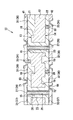
図1には、本実施形態の積層樹脂配線基板11が概略的に示されている。この積層樹脂配線基板11は、Fe−Ni系圧延合金の一種であるアンバーからなる金属板(以下「圧延アンバー板12」と呼ぶ。)をコア材として備えている。図1において圧延アンバー板12の上面(即ち第1主面)13及び下面(即ち第2主面)14には、それぞれビルドアップ層が形成されている。
【0034】
圧延アンバー板12の厚さは0.25mmに設定されていて、その所定箇所には上面13及び下面14を連通させる0.30mmφの金属板貫通孔15が多数透設されている。
【0035】
上面13の側のビルドアップ層は、樹脂絶縁層21,41と配線層31とを交互に積層した構造を有している。下面14の側のビルドアップ層は、樹脂絶縁層22,42と配線層32とを交互に積層した構造を有している。即ち、本実施形態では積層樹脂配線基板11の両側において配線層31,32の層数が等しくなっている。上記配線層31,32は、圧延アンバー板12との間に所定の絶縁信頼性が要求される第1の導体パターン37と、圧延アンバー板12との間に前記第1の導体パターン37よりもさらに高い絶縁信頼性が要求される第2の導体パターン38とからなる。本実施形態では、かかる第2の導体パターン38は、圧延アンバー板12の上面13の側及び下面14の側のそれぞれに存在している。
【0036】
圧延アンバー板12の上面13において第2の導体パターン38に対面する箇所には、非貫通の孔部の一態様である溝部18が設けられている。一方、圧延アンバー板12の下面14において第2の導体パターン38に対面する箇所には、非貫通の孔部の一態様である溝部19が設けられている。本実施形態における溝部18,19は、第2の導体パターン38の延びる方向に沿って略平行に形成されている(図7参照)。溝部18,19の幅は第2の導体パターン38の線幅よりも1.5倍〜3倍程度大きくなるように設定されている。溝部18,19の深さはともに等しく、圧延アンバー板12の厚さの約1/4に設定されている。
【0037】
なお、圧延アンバー板12を上面13側から見た場合、上面13側に設けられた溝部18と、下面14側に設けられた溝部19とが重なり合わないように、これらを基板面方向にずらした状態で配置している。
【0038】
第1層めの樹脂絶縁層21,22は、その厚さが25μmであって、連続多孔質PTFEにエポキシ樹脂を含浸させた樹脂−樹脂複合材料からなる。第1層めの樹脂絶縁層21,22は、圧延アンバー板12の上面13及び下面14の上に形成されている。なお、金属板貫通孔15内には、前記樹脂−樹脂複合材料に由来するエポキシ樹脂が充填されることにより、樹脂充填体23が形成されている。
【0039】
配線層31,32はいずれも厚さ約15μm(15〜40μm)の銅からなり、第1層めの樹脂絶縁層21,22上にそれぞれ形成されている。第1層めの樹脂絶縁層21,22には直径70μmのビアホール形成用孔33が形成されている。ビアホール形成用孔33の内部には無電解銅めっきによりビア導体35が形成され、これによりブラインドビアホール導体34(第1のビアホール導体)が構成されている。そして、このブラインドビアホール導体34を介して、圧延アンバー板12−配線層31間、圧延アンバー板12−配線層32間がそれぞれ接続導通されている。
【0040】
第2層めの樹脂絶縁層41,42は、その厚さが20μmであって、感光性エポキシ樹脂を用いて第2層めの樹脂絶縁層21,22上に形成されている。第2層めの樹脂絶縁層41,42にはビアホール形成用孔63,64が透設されている。ビアホール形成用孔63,64内には、銅めっき層、ニッケルめっき層及び金フラッシュめっき層(いずれも図示しない)という3層の導体からなるすり鉢状のパッド71,72が形成されている。パッド71の底部は配線層31に対して接続導通されていて、パッド72の底部は配線層32に対して接続導通されている。なお、これらのパッド71,72は、図示しないICチップやマザーボード等の接続端子に対し、はんだ付け等により接続されるようになっている。第2層めの樹脂絶縁層41,42は、ソルダレジスト層としての役割も有している。
【0041】
第1層めの樹脂絶縁層21,22及び樹脂充填体23には、それらを貫通する直径0.15mmのビアホール形成用孔25が形成されている。ビアホール形成用孔25の内部には銅めっきからなるビア導体27が形成され、その結果として金属板絶縁ビアホール導体26(第2のビアホール導体)が構成されている。金属板絶縁ビアホール導体26は、圧延アンバー板12の金属板貫通孔15の内壁面との間で絶縁を保ちつつ、上面側の配線層31と下面側の配線層32との間を接続導通している。
【0042】
そして、このような積層樹脂配線基板11に図示しないICチップ等を搭載すれば、いわゆるメタルコアパッケージを得ることができる。かかるパッケージに対して通電を行った場合、圧延アンバー板12は、ブラインドビアホール導体34を通じて所定の電位(接地電位または電源電位など)となり、グランド層または電源層として機能するようになっている。
【0043】
次に、上記構成の積層樹脂配線基板11を製造する手順について説明する。
【0044】
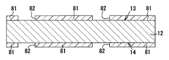
まず、厚さ0.25mmの圧延アンバー板12を用意する(図2参照)。そして、この圧延アンバー板12の上面13及び下面14の上に、感光性レジストを形成し、露光・現像を行うことにより、所定パターンを有する金属板貫通孔形成用マスク81を形成する。かかるマスク81において金属板貫通孔15が形成されるべき箇所には、開口部82が設けられる(図3参照)。
【0045】
この状態で、Fe−Ni合金を溶解しうる従来公知のエッチャント(ここでは塩化第二鉄)により圧延アンバー板12を両面から同時にエッチングする。ここでは、エッチングによる侵蝕部同士が内部にて確実に連通するような条件を設定すべく、片面側からのエッチング深さを圧延アンバー板12の厚さの半分以上(具体的には0.15mm程度)に設定している。
【0046】
そして、このような条件にて両面同時エッチングを行うと、上面13及び下面14の両方から圧延アンバー板12が侵蝕され、侵蝕部同士が内部で互いに連通する結果、開口部82のある位置に金属板貫通孔15が形成される。その後、不要となったマスク81を専用の剥離液で溶解除去する(図4参照)。
【0047】
次に、この圧延アンバー板12の上面13及び下面14の上に、感光性レジストを形成し、露光・現像を行うことにより、先ほどのものとは異なるパターンを有する溝部形成用マスク91を形成する。かかるマスク91において溝部18,19が形成されるべき箇所には、開口部92が設けられる(図5参照)。
【0048】
この状態で、Fe−Ni合金を溶解しうる上記エッチャントにより圧延アンバー板12を両面から同時にエッチングする。ただし、ここではエッチングによる侵蝕部同士が内部にて連通しないような条件を設定することにより、ハーフエッチングを行うようにする。即ち、片面側からのエッチング深さを圧延アンバー板12の厚さの1/4程度(具体的には0.06mm程度)に設定する。
【0049】
そして、このような条件にて両面同時エッチングを行うと、上面13及び下面14の両方から圧延アンバー板12が侵蝕され、開口部92のある位置に溝部18,19(非貫通の孔部)がそれぞれ形成される。その後、不要となったマスク91を専用の剥離液で溶解除去する(図6,図7参照)。
【0050】
次に、前記圧延アンバー板12に対し、第1層めの樹脂絶縁層21,22及び樹脂充填体23を形成する。ここでは、まず、前記圧延アンバー板12の上面13及び下面14に、それぞれ連続多孔質PTFEに半硬化のエポキシ樹脂を含浸させたプリプレグ(図示略)を介して、厚さ20μmの銅箔83,84を重ね合わせる。そして、このような積層物を真空熱プレス機(図示しない)によって真空熱圧着することにより、半硬化状態であったプリプレグを本硬化させ、これにより厚さ30μmの樹脂絶縁層21,22を各々形成する。このとき、金属板貫通孔15内には、プリプレグから滲出したエポキシ樹脂が充填される結果、樹脂充填体23が形成される(図8参照)。なお、このとき溝部18,19も、プリプレグから滲出したエポキシ樹脂によって完全に埋められる。
【0051】
次に、YAGレーザまたは炭酸ガスレーザを用いたレーザ孔あけ加工を実施することにより、第1層めの樹脂絶縁層21,22、樹脂充填体23、銅箔83,84を穿孔し、直径70μmのビアホール形成用孔25,33を形成する。なお、本実施形態では、圧延アンバー板12を穿孔しないような条件にレーザ出力等を設定する必要がある。
【0052】
次に、従来公知の手法によって、ビアホール形成用孔33内にビア導体35を形成し、かつビアホール形成用孔25内にビア導体27を形成する。その結果、ブラインドビアホール導体34及び金属板絶縁ビアホール導体26が形成される(図9参照)。また、従来公知の手法によって、第1層めの樹脂絶縁層21の上、及び樹脂絶縁層22の下面の上に、それぞれ第1層めの配線層31,32をパターン形成する。なお、配線層31,32を構成する導体パターン37,38のうち、より高い絶縁信頼性が要求される第2の導体パターン38については、溝部18,19に対応して配置するようにパターニングを行う。
【0053】
具体的には、無電解銅めっきの後、露光・現像を行って所定パターンのめっきレジストを形成する。この状態で無電解銅めっき層を共通電極として電解銅めっきを施した後、まずレジストを溶解除去して、さらに不要な無電解銅めっき層をエッチングで除去する。
【0054】
次に、ブラインドビアホール導体34及び金属板絶縁ビアホール導体26の内部にエポキシ樹脂を充填し、これを硬化させることにより、プラグ体28を形成する。さらに、第1層めの樹脂絶縁層21,22の上にプリプレグを介して銅箔83,84を重ね合わせ、真空熱プレスにより圧着硬化させる。その結果、第2層めの樹脂絶縁層41,42及び銅箔83,84を積層形成する(図10参照)。
【0055】
次に、レーザー孔あけ加工を実施することにより、ビアホール形成用孔63,64を穿孔し、かつビア導体を形成する。さらに、銅箔83,84上及びビアホール形成用孔63,64上に、従来公知の手法を用いて無電解銅めっきを行う。次に、前記電解銅めっき及び銅箔83,84のうち不要部分をエッチングし、無電解ニッケルめっき、無電解金めっきを順次施すことにより、パッド71,72を形成する。以上の結果、図1に示す積層樹脂配線基板11が完成する。
【0056】
従って、本実施形態によれば以下のような効果を得ることができる。
【0057】
(1)本実施形態の積層樹脂配線基板11では、第1の導体パターン37よりもさらに高い絶縁信頼性が要求される第2の導体パターン38があったとしても、圧延アンバー板12においてそれに対面する箇所には溝部18,19が設けられている。そして、溝部18,19が設けられた箇所については、第2の導体パターン38から圧延アンバー板12の表面までの距離が大きくなる。このため、樹脂絶縁層21,22の厚さを第1の導体パターン37に必要とされる絶縁厚みに設定したとしても、第1の導体パターン37と圧延アンバー板12の間の絶縁信頼性のみならず、第2の導体パターン38と圧延アンバー板12との間の絶縁信頼性も確保される。また、本実施形態によると、樹脂絶縁層21,22の厚さを第1の導体パターン37に必要とされる絶縁厚みに設定すればよくなるため、基板厚さ方向の寸法を十分に抑えることが可能となる。よって、積層樹脂配線基板11の軽薄短小化の要請に確実に応えることができる。
【0058】
(2)また、ハーフエッチング法を利用した本実施形態の製造方法によると、上記の優れた積層樹脂配線基板11を、比較的容易にかつ生産性及びコスト性を低下させることなく確実に得ることができる。
【0059】
なお、本発明の実施形態は以下のように変更してもよい。
【0060】
・図11には別の実施形態の積層樹脂配線基板11が示されている。この積層樹脂配線基板11では、前記実施形態のものに比べて溝部18,19が深く、圧延アンバー板12(金属板)の厚さの半分以上になっている。この積層樹脂配線基板11は、例えば、金属板貫通孔用マスクを兼ねる溝部形成用マスク101を用いて形成可能である。つまり、このマスク101において溝部18,19が形成されるべき箇所には開口部92が設けられ、金属板貫通孔15が形成されるべき箇所には開口部82が設けられている(図12参照)。従って、両面同時エッチングを行うと、溝部18,19及び金属板貫通孔15が同時に形成される(図13参照)。よって、前記実施形態のときと比べてマスク数が1つ少なくて済み、その分だけ工数を減らすことができる。
【0061】
・溝部18,19(非貫通の孔部)の形成方法は、実施形態にて示したようなエッチング法のみに限定されず、それ以外の方法であってもよい。例えば、研削等の機械的加工法を採用してもよいほか、金型で押圧することにより部分的に凹みを造るという加工法を採用してもよい。
【0062】
・第2の導体パターン38に対面して設けられる溝部18,19は、実施形態ではその周囲にある金属板貫通孔15と全く連結しない状態で設けられていたが、これを金属板貫通孔15と部分的に連結する状態で設けてもよい。
【0063】
・また、樹脂絶縁層21,22,41,42として、連続多孔質PTFEにエポキシ樹脂を含浸させたプリプレグを硬化させたものを用いたが、その他の材質でもよいことは明らかであり、例えば、ガラス繊維−エポキシ樹脂複合材料などを用いることができる。
【0064】
・上記実施形態では、圧延アンバー板12(金属板)をコア材として1枚のみ使用した積層樹脂配線基板11の具体例を示した。本発明は勿論このような態様のみに限定されることはない。例えば、上記圧延アンバー板12(金属板)を2枚またはそれ以上の枚数使用した積層樹脂配線基板として具体化することも可能である。このような構造であれば、基板全体の低熱膨張化をより確実に達成できることに加え、2枚以上あるコア材にさまざまな機能を担わせることができる。このため、よりいっそうの高信頼化・高機能化を達成することが可能となる。
【0065】
・上記実施形態では、コア材の上下にそれぞれ同数の樹脂絶縁層21,22、41,42及び配線層31,32を形成したが、これに限定されることはなく、上下にて異なる数にしても勿論よい。また、配線層31,32の層数を片面について2層またはそれ以上にして、さらなる多層化を図っても勿論よい。
【0066】
・上記実施形態では、圧延アンバー板12(金属板)をコア材として用い、その上下にビルドアップ層を有する積層樹脂配線基板11の具体例を示した。本発明は勿論このような態様のみに限定されることはない。例えば、前記圧延アンバー板12(金属板)をベース材として用い、その上下いずれか片面のみにビルドアップ層を有する積層樹脂配線基板(いわゆるメタルベース基板)として具体化することも可能である。
【0067】
次に、特許請求の範囲に記載された技術的思想のほかに、前述した実施形態によって把握される技術的思想を以下に列挙する。
【0068】
(1)前記溝部の幅は前記第2の導体パターンの線幅よりも大きくなるように設定されていることを特徴とする請求項3に記載の積層樹脂配線基板。
【0069】
(2)前記溝部の幅は前記第2の導体パターンの線幅の1.5倍〜10倍(特には1.5倍〜3倍)に設定されていることを特徴とする請求項3に記載の積層樹脂配線基板。
【0070】
(3)前記非貫通の孔部の深さは、前記金属板の厚さの半分未満(前記金属板の厚さの1/100〜1/3、特には1/10〜1/3)に設定されていることを特徴とする請求項2または3に記載の積層樹脂配線基板。
【0071】
(4)前記金属板における前記第1主面及び前記第2主面の両方に非貫通の孔部を形成する場合、前記第1主面側に設けられた非貫通の孔部と、前記第2主面側に設けられた非貫通の孔部とが前記第1主面側から見て重なり合わないように、これらを基板面方向にずらした状態で配置することを特徴とする請求項2または3に記載の積層樹脂配線基板。
【0072】
(5)前記孔部内には絶縁層形成用の樹脂が埋まっていることを特徴とする請求項2または3に記載の積層樹脂配線基板。
【0073】
(6)第1主面及び第2主面を有する厚さ150μm以上の圧延Fe−Ni系合金材からなる金属板と、前記金属板の第1主面側及び第2主面側に位置する複数の配線層と、前記金属板と前記配線層との間、または前記金属板と前記配線層との間及び前記配線層間に介在する複数の樹脂絶縁層と、前記樹脂絶縁層に形成され、前記配線層と前記金属板との間を接続導通する第1のビアホール導体と、前記金属板の前記第1主面及び前記第2主面を連通させる金属板貫通孔内に充填された樹脂充填体と、前記樹脂充填体を貫通するビアホール形成用孔内に形成され、前記金属板との間で絶縁を保ちつつ前記第1主面側の配線層と第2主面側の配線層との間を接続導通する第2のビアホール導体とを備え、前記配線層は、前記金属板との間に所定の絶縁信頼性が要求される第1の導体パターンと、前記金属板との間に前記第1の導体パターンよりもさらに高い絶縁信頼性が要求される第2の導体パターンとを有するとともに、前記金属板において前記第2の導体パターンに対面する箇所には、前記第2の導体パターンの延びる方向に沿って略平行に形成され、その幅が前記第2の導体パターンの線幅よりも大きくなるように設定され、その深さが前記金属板の厚さの半分未満に設定された溝部が設けられていることを特徴とする積層樹脂配線基板。
【図面の簡単な説明】
【図1】本発明を具体化した実施形態の積層樹脂配線基板を示す部分断面概略図。
【図2】同配線基板の構成部材である圧延アンバー板を示す部分断面概略図。
【図3】圧延アンバー板にフォトエッチング用マスクを形成した状態を示す部分断面概略図。
【図4】フォトエッチングにより金属板貫通孔を形成した状態を示す部分断面概略図。
【図5】圧延アンバー板に別のフォトエッチング用マスクを形成した状態を示す部分断面概略図。
【図6】フォトエッチングにより溝部を形成した状態を示す部分断面概略図。
【図7】フォトエッチングにより溝部を形成した状態を示す部分平面図。
【図8】第1層めの樹脂絶縁層及び銅箔を積層した状態を示す部分断面概略図。
【図9】第1層めの樹脂絶縁層に各種ビアホール導体を形成した状態を示す部分断面概略図。
【図10】第2層めの樹脂絶縁層及び銅箔を積層した状態を示す部分断面概略図。
【図11】本発明を具体化した別の実施形態の積層樹脂配線基板を示す部分断面概略図。
【図12】前記積層樹脂配線基板の製造にあたり、圧延アンバー板にフォトエッチング用マスクを形成した状態を示す部分断面概略図。
【図13】フォトエッチングにより溝部を形成した状態を示す部分断面概略図。
【符号の説明】
11…積層樹脂配線基板
12…金属板である圧延アンバー板
13…第1主面である上面
14…第2主面である下面
18,19…孔部としての溝部
21,22,41,42…樹脂絶縁層
31,32…配線層
37…配線層を構成する第1の導体パターン
38…配線層を構成する第2の導体パターン[0001]
BACKGROUND OF THE INVENTION
The present invention relates to a laminated resin wiring board and a method for manufacturing the same, and more particularly to a laminated resin wiring board characterized by the structure of a metal plate used as a core material or a base material and a method for manufacturing the same.
[0002]
[Prior art]
In recent years, with the miniaturization of electrical equipment, electronic equipment, etc., miniaturization and high density are also required for wiring boards mounted on these equipments. In order to meet such market demand, multilayer circuit board technology has been studied. As a multilayering method, a so-called build-up method in which insulating layers and wiring layers are alternately laminated and integrated with a core material or a base material is generally employed. As this type of conventional wiring board, a metal core board or a metal base board using a metal plate is known for improving heat dissipation and reducing the thermal expansion coefficient of the whole board (Japanese Patent Laid-Open No. 2000-133913). reference).
[0003]
By the way, among the wiring layers of the metal core substrate and the metal base substrate, particularly those that are closest to the metal plate need to ensure a predetermined insulation reliability with the metal plate. And the insulation reliability about this part will depend on the physical characteristic, thickness, etc. of resin used as an insulating layer fundamentally.
[0004]
[Problems to be solved by the invention]
In recent metal core substrates and metal base substrates, there is a strong demand for lightness and reduction in size. Therefore, it is required to reduce the thickness of the insulating layer as much as possible in order to suppress the dimension in the substrate thickness direction. Such a thinning of the insulating layer is also required from the viewpoint of improving the hole workability when a via hole is formed in the insulating layer.
[0005]
However, when the resin insulation layer is further thinned, it is very difficult to ensure the insulation reliability between the wiring layer and the metal plate. In particular, a conductor pattern that is required to have higher insulation reliability than a normal conductor pattern (referred to as “first conductor pattern” for convenience) between the metal plate and the metal plate (referred to as “second conductor pattern” for convenience). ), This problem becomes more prominent.
[0006]
That is, if the thickness of the insulating layer is set to the insulating thickness required for the first conductor pattern, the insulating thickness is insufficient for the second conductor pattern that requires higher insulation reliability than that. End up. Therefore, at present, in order to ensure the insulation reliability of both, the thickness of the insulating layer has to be set to the insulation thickness required for the second conductor pattern. Therefore, the insulating layer becomes thick to some extent, and the dimension in the substrate thickness direction cannot be sufficiently suppressed.
[0007]
SUMMARY OF THE INVENTION The present invention has been made in view of the above-mentioned problems, and an object of the present invention is to provide a laminated resin wiring board excellent in insulation reliability between the wiring layer and the metal plate while suppressing the dimension in the substrate thickness direction, and its It is to provide a manufacturing method.
[0008]
[Means, actions and effects for solving the problems]
Solution means for solving the above-described problems include a metal plate having a first main surface and a second main surface, and a wiring located on at least one of the first main surface and the second main surface. And a resin insulating layer interposed between the metal plate and the wiring layer, and the wiring layer includes a first conductor pattern required to have a predetermined insulation reliability between the metal plate and the metal layer. And a second conductor pattern that is required to have a higher insulation reliability than the first conductor pattern between the metal plate and a portion facing the second conductor pattern on the metal plate. The gist of the present invention is a laminated resin wiring board provided with holes.
[0009]
Therefore, according to the above invention, even if there is a second conductor pattern that requires higher insulation reliability than the first conductor pattern, the metal plate is provided with a hole at a location facing it. . And about the location in which the hole part was provided, the distance from the 2nd conductor pattern to the surface of a metal plate becomes large. Therefore, even when the thickness of the insulating layer is set to the insulating thickness required for the first conductor pattern, not only the insulation reliability between the first conductor pattern and the metal plate but also the second conductor Insulation reliability between the pattern and the metal plate is also ensured. In addition, according to the present invention, the thickness of the insulating layer may be set to an insulating thickness required for the first conductor pattern, so that the dimension in the substrate thickness direction can be sufficiently suppressed.
[0010]
The metal plate is appropriately selected in consideration of conductivity, cost, and ease of drilling when drilling. Examples of suitable metal plates include copper plates, copper alloy plates, and plate materials made of simple metals or alloys other than copper. Examples of the copper alloy include aluminum bronze (Cu—Al series), phosphor bronze (Cu—P series), brass (Cu—Zn series), cupronickel (Cu—Ni series), and the like. Examples of simple metals other than copper include aluminum, iron, chromium, nickel, molybdenum and the like. Examples of alloys other than copper include stainless steel (iron alloy such as Fe—Cr and Fe—Cr—Ni), amber (Fe—Ni alloy, 36% Ni), so-called 42 alloy (Fe—Ni alloy, 42 % Ni), so-called 50 alloy (Fe—Ni alloy, 50% Ni), nickel alloy (Ni—P, Ni—B, Ni—Cu—P), cobalt alloy (Co—P, Co—) B series, Co-Ni-P series), tin alloys (Sn-Pb series, Sn-Pb-Pd series) and the like.
[0011]
Among these, in particular, a plate material made of an Fe—Ni alloy such as amber, 42 alloy, or 50 alloy is preferably used as the metal plate. That is, since the Fe—Ni-based alloy has a property that its thermal expansion coefficient is smaller than that of copper, the thermal expansion of the entire substrate can be reduced by using it as a metal plate for a laminated resin wiring board. Because. In addition, Fe-Ni alloy is suitable for high added value because it is suitable for high added value because it is suitable for high added value though it is inferior to copper and has suitable conductivity. That's why. Furthermore, although Fe—Ni-based alloys are suitable for copper, although they are inferior to copper, high heat dissipation can be achieved by using them as metal plates for laminated resin wiring boards. .
[0012]
In addition, the thickness of the metal plate is not particularly limited, but to be strong, it is preferably 150 μm or more, more preferably 150 μm to 500 μm, and particularly preferably 150 μm to 300 μm. The reason for this is that if the thickness of the metal plate is less than 150 μm, the rigidity of the metal plate itself is reduced, so that wrinkles and scratches are likely to occur during the manufacturing process, resulting in a decrease in handleability and a decrease in yield. Because it leads to. On the other hand, if the thickness of the metal plate is 500 μm, there is no problem with respect to rigidity, but the laminated resin wiring board is not only thickened, but hole processing becomes difficult. In addition, when thickness is 150 micrometers or more as mentioned above, it is good to use a rolled metal material from viewpoints, such as cost property and productivity.
[0013]
The wiring layer may be located on both sides of the first main surface and the second main surface of the metal plate, and may be located only on the first main surface side or only on the second main surface side. Such a metal material for forming the wiring layer and a method for forming the wiring layer can be appropriately selected in consideration of conductivity, adhesion to the resin insulating layer, and the like. Examples of the metal material for forming the wiring layer include copper, copper alloy, nickel, nickel alloy, tin, tin alloy and the like. Such a wiring layer can be formed by a known method such as a subtractive method, a semi-additive method, or a full additive method. Specifically, for example, techniques such as etching of copper foil, electroless copper plating or electrolytic copper plating, electroless nickel plating or electrolytic nickel plating can be used. It is also possible to form a wiring layer by etching after forming a metal layer by a technique such as sputtering or CVD, or to form a wiring layer by printing a conductive paste or the like.
[0014]
The resin insulating layer interposed between the metal plate and the wiring layer can be appropriately selected in consideration of insulation, heat resistance, moisture resistance, and the like. Preferable examples of the resin material forming the resin insulating layer include EP resin (epoxy resin), PI resin (polyimide resin), BT resin (bismaleimide-triazine resin), PPE resin (polyphenylene ether resin) and the like. In addition, composite materials of these resins and organic fibers such as glass fibers (glass woven fabrics and glass nonwoven fabrics) and polyamide fibers, or three-dimensional network fluorine-based resin base materials such as continuous porous PTFE, epoxy resins, etc. A resin-resin composite material impregnated with a thermosetting resin may be used.
[0015]
Further, one or more resin insulation layers may be formed on the surface of the resin insulation layer formed on the main surface of the metal plate, and a wiring layer is formed on each resin insulation layer. It may be. In other words, the above laminated resin wiring board may be provided with only a resin insulating layer interposed between the metal plate and the wiring layer, or between the metal plate and the wiring layer and between different wiring layers. It may be provided with a plurality of resin insulation layers intervening.
[0016]
The laminated resin wiring board may be provided with a via-hole conductor (that is, a first via-hole conductor) that is formed in a resin insulating layer and connects and conducts between the wiring layer and the metal plate. This is because the presence of such a via-hole conductor allows the metal plate to function as a ground layer or a power supply layer. The first via-hole conductor is not limited to the one that conducts connection between the wiring layer located on the innermost layer and the metal plate, but connects between the wiring layer located on the outer layer side and the metal plate. It may be conductive.
[0017]
When the wiring layer and the resin insulating layer are present on both sides of the first main surface and the second main surface of the metal plate, the metal plate is formed with a metal plate through hole that communicates the first main surface and the second main surface. In addition, it is preferable that the inside be filled with a resin filler.
[0018]
Here, the resin filler can be appropriately selected in consideration of insulation, heat resistance, moisture resistance, and the like. Preferable examples of the resin material forming the resin filler include EP resin, PI resin, BT resin, PPE resin, and the like. That is, as long as it can be used as the resin material for forming the resin insulating layer, it can be used without any problem as the resin material for forming the resin filler. In addition, it is preferable from a viewpoint of cost efficiency or productivity to use what was used as the resin material for resin insulation layer as it is as a resin material for resin filler formation.
[0019]
Further, the laminated resin wiring board has a second via-hole conductor (that is, a metal that connects and connects the wiring layer on the first main surface side and the wiring layer on the second main surface side while maintaining insulation with the metal plate. (Plate insulating via-hole conductor), which may be formed by forming a via conductor in a via-hole forming hole penetrating the resin filler. In this case, the via hole forming hole can be formed by, for example, photoetching or drilling.
[0020]
The above-mentioned laminated resin wiring board connects and continually connects the wiring layers on both main surfaces while maintaining a connection conduction state with another via hole conductor different from the first and second via hole conductors, for example, a metal plate. A via hole conductor (that is, a metal plate conduction via hole conductor) or the like may be provided.
[0021]
Here, the method for forming the metal plate through-hole in the metal plate is not particularly limited, and various conventionally known hole-piercing methods can be employed. Examples of such methods include etching, laser processing, punching, and the like, but it is desirable to employ etching (especially double-sided simultaneous etching) when the metal plate is thick. Furthermore, it is desirable to employ photo-etching. In this case, it is possible to increase the positional accuracy of the metal plate through-hole formed, and to improve the yield.
[0022]
The “hole” provided in the metal plate refers to a concave structure that can substantially increase the distance from the second conductor pattern to the surface of the metal plate. The hole may or may not penetrate, but is preferably a non-through hole.
[0023]
The reason for this is that the configuration in which the non-penetrating hole is provided is less likely to be accompanied by a decrease in strength of the metal plate and less likely to be accompanied by a decrease in heat dissipation due to a decrease in volume of the metal plate. Further, since the non-through hole portion has a high degree of freedom in layout, it is advantageous in designing when the second conductor pattern is present on both main surface sides.
[0024]
The non-penetrating hole is preferably a groove formed substantially in parallel along the direction in which the second conductor pattern extends.
[0025]
This is because the distance from the surface of the metal plate can be increased over the entire extending direction of the second conductor pattern, and sufficient insulation reliability can be ensured between the metal plate and the second conductor pattern.
[0026]
When the hole is a groove, it is desirable that the width of the groove is set to be larger than the line width of the second conductor pattern. It is preferable to set 5 times to 10 times, particularly 1.5 times to 3 times. The reason is that if the width of the groove is the same as or smaller than the line width of the second conductor pattern, the distance from the metal plate is reduced at both edges of the second conductor pattern, and sufficient insulation reliability is achieved. This is because it is difficult to ensure the sex. Further, if the width of the groove is less than 1.5 times the line width of the second conductor pattern, it may be difficult to ensure sufficient insulation reliability depending on the dimensional tolerance of the second conductor pattern. . Conversely, the formation of a groove having a width exceeding 10 times the line width of the second conductor pattern may be difficult due to the space in the metal plate.
[0027]
The depth of the non-penetrating hole is preferably less than half of the thickness of the metal plate, specifically 1/100 to 1/3, particularly 1/10 to the thickness of the metal plate. It is good to set to 1/3. The reason is that if the hole is too shallow, the distance from the second conductor pattern to the surface of the metal plate cannot be made sufficiently large. On the other hand, if the hole is too deep, the strength and heat dissipation of the metal plate may be lowered in some cases. When forming non-through holes on both main surfaces of the metal plate, the depth may be set the same on the first main surface side and the second main surface side, or set differently. May be. However, it is generally more advantageous in terms of the process to form holes having the same depth on both sides.
[0028]
When forming non-penetrating holes on both main surfaces of the metal plate, non-penetrating holes (grooves) provided on the first main surface side and non-penetrating holes provided on the second main surface side It is desirable to dispose these in a state of being shifted in the substrate surface direction so that they do not overlap with the (groove portion) when viewed from the first main surface side. The reason is to prevent a reduction in the strength of the metal plate due to the occurrence of overlapping and thin portions.
[0029]
The hole is preferably filled with an insulating material, and more specifically, a resin for forming an insulating layer is preferably buried. The reason is that if a hole is provided in the metal plate and nothing is buried there (that is, there is a void), the adhesion between the metal plate and the resin insulating layer is likely to decrease, and reliability is improved. This is because the achievement of the objective is hindered.
[0030]
Another solution includes a step of forming a non-penetrating hole by a half-etching method at a predetermined location in a metal plate having a first main surface and a second main surface, and the metal in which the hole is formed. A predetermined insulation reliability is required between the step of forming a resin insulating layer on at least one of the first main surface and the second main surface of the plate and the metal plate. And forming a wiring layer on the resin insulating layer having a second conductive pattern that requires higher insulation reliability than the first conductive pattern between the conductive pattern and the metal plate, In that case, the gist is a method for manufacturing a laminated resin wiring board, including a step of arranging the second conductor pattern corresponding to the hole.
[0031]
Therefore, according to the said invention, a non-through-hole is comparatively easily formed by partially eroding a metal plate by a half etching method. Thereafter, by forming a resin insulating layer on the metal plate in which the hole is formed, the hole is filled with the resin material for forming the insulating layer. If the second conductor pattern is formed as described above, the second conductor pattern is in a position just corresponding to the hole, and the distance from the second conductor pattern to the surface of the metal plate is increased. Therefore, according to this manufacturing method, the above excellent laminated resin wiring substrate can be obtained relatively easily. Here, the half-etching method refers to a method of stopping the etching hole halfway without completely penetrating the etching hole when the substrate is eroded from one side surface by the etchant. When such a half-etching method is used, for example, the formation of a metal plate through hole and the formation of a non-through hole can be performed simultaneously, and a reduction in productivity and cost can be avoided.
[0032]
DETAILED DESCRIPTION OF THE INVENTION
Hereinafter, a laminated resin wiring board (so-called metal core board) according to an embodiment of the present invention will be described in detail with reference to FIGS.
[0033]
FIG. 1 schematically shows the laminated
[0034]
The thickness of the rolled
[0035]
The buildup layer on the
[0036]
On the
[0037]
The rolled
[0038]
The first resin insulation layers 21 and 22 have a thickness of 25 μm and are made of a resin-resin composite material in which continuous porous PTFE is impregnated with an epoxy resin. The first resin insulation layers 21 and 22 are formed on the
[0039]
Each of the wiring layers 31 and 32 is made of copper having a thickness of about 15 μm (15 to 40 μm), and is formed on the first
[0040]
The second resin insulation layers 41 and 42 have a thickness of 20 μm and are formed on the second resin insulation layers 21 and 22 using a photosensitive epoxy resin. Via
[0041]
The first resin insulation layers 21 and 22 and the
[0042]
A so-called metal core package can be obtained by mounting an IC chip or the like (not shown) on such a laminated
[0043]
Next, a procedure for manufacturing the laminated
[0044]
First, a rolled
[0045]
In this state, the rolled
[0046]
When the double-sided simultaneous etching is performed under such conditions, the rolled
[0047]
Next, a photosensitive resist is formed on the
[0048]
In this state, the rolled
[0049]
When the double-sided simultaneous etching is performed under such conditions, the rolled
[0050]
Next, first resin insulation layers 21 and 22 and a
[0051]
Next, by carrying out laser drilling using a YAG laser or a carbon dioxide laser, the first resin insulation layers 21 and 22, the
[0052]
Next, a via
[0053]
Specifically, after electroless copper plating, exposure / development is performed to form a predetermined pattern of plating resist. In this state, after electrolytic copper plating is performed using the electroless copper plating layer as a common electrode, first, the resist is dissolved and removed, and further unnecessary electroless copper plating layer is removed by etching.
[0054]
Next, an epoxy resin is filled in the blind via-
[0055]
Next, by carrying out laser drilling, via-
[0056]
Therefore, according to the present embodiment, the following effects can be obtained.
[0057]
(1) In the laminated
[0058]
(2) Further, according to the manufacturing method of the present embodiment using the half etching method, the above excellent laminated
[0059]
In addition, you may change embodiment of this invention as follows.
[0060]
FIG. 11 shows a laminated
[0061]
-The formation method of the
[0062]
In the embodiment, the
[0063]
In addition, as the
[0064]
In the above embodiment, a specific example of the laminated
[0065]
In the above embodiment, the same number of
[0066]
In the above embodiment, a specific example of the laminated
[0067]
Next, in addition to the technical ideas described in the claims, the technical ideas grasped by the embodiment described above are listed below.
[0068]
(1) The laminated resin wiring board according to claim 3, wherein the width of the groove is set to be larger than the line width of the second conductor pattern.
[0069]
(2) The width of the groove is set to 1.5 to 10 times (particularly 1.5 to 3 times) the line width of the second conductor pattern. The laminated resin wiring board described.
[0070]
(3) The depth of the non-penetrating hole is less than half of the thickness of the metal plate (1/100 to 1/3, particularly 1/10 to 1/3 of the thickness of the metal plate). The laminated resin wiring board according to claim 2, wherein the laminated resin wiring board is set.
[0071]
(4) When a non-penetrating hole is formed in both the first main surface and the second main surface of the metal plate, the non-penetrating hole provided on the first main surface side, and the first 3. The non-through holes provided on the two principal surface sides are arranged in a state of being shifted in the substrate surface direction so as not to overlap each other when viewed from the first principal surface side. Or the laminated resin wiring board of 3.
[0072]
(5) The laminated resin wiring board according to claim 2 or 3, wherein a resin for forming an insulating layer is buried in the hole.
[0073]
(6) A metal plate made of a rolled Fe—Ni alloy material having a first main surface and a second main surface and having a thickness of 150 μm or more, and located on the first main surface side and the second main surface side of the metal plate. A plurality of wiring layers, a plurality of resin insulating layers interposed between the metal plate and the wiring layer, or between the metal plate and the wiring layer and between the wiring layers, and formed in the resin insulating layer, A first via-hole conductor that connects and connects the wiring layer and the metal plate, and a resin filling that fills the metal plate through-hole that communicates the first main surface and the second main surface of the metal plate And a wiring layer on the first main surface side and a wiring layer on the second main surface side while maintaining insulation between the body and the via hole forming hole penetrating the resin filler. A second via-hole conductor connecting and conducting between the wiring layers, and the wiring layer between the metal plate A first conductor pattern that requires insulation reliability; and a second conductor pattern that requires higher insulation reliability than the first conductor pattern between the metal plate and the metal. A portion of the plate facing the second conductor pattern is formed substantially in parallel along the direction in which the second conductor pattern extends, and the width thereof is larger than the line width of the second conductor pattern. The laminated resin wiring board is characterized in that a groove portion whose depth is set to less than half of the thickness of the metal plate is provided.
[Brief description of the drawings]
FIG. 1 is a schematic partial cross-sectional view showing a laminated resin wiring board according to an embodiment of the present invention.
FIG. 2 is a partial cross-sectional schematic view showing a rolled amber plate that is a component of the wiring board.
FIG. 3 is a partial cross-sectional schematic view showing a state where a photoetching mask is formed on a rolled amber plate.
FIG. 4 is a partial cross-sectional schematic view showing a state where metal plate through holes are formed by photoetching.
FIG. 5 is a partial cross-sectional schematic view showing a state in which another photoetching mask is formed on a rolled amber plate.
FIG. 6 is a partial cross-sectional schematic view showing a state in which a groove is formed by photoetching.
FIG. 7 is a partial plan view showing a state in which a groove is formed by photoetching.
FIG. 8 is a partial cross-sectional schematic view showing a state in which a first resin insulating layer and a copper foil are laminated.
FIG. 9 is a partial cross-sectional schematic view showing a state in which various via-hole conductors are formed in the first resin insulating layer.
FIG. 10 is a partial cross-sectional schematic view showing a state in which a second resin insulating layer and a copper foil are laminated.
FIG. 11 is a partial cross-sectional schematic view showing a laminated resin wiring board of another embodiment embodying the present invention.
FIG. 12 is a partial cross-sectional schematic view showing a state in which a photoetching mask is formed on a rolled amber plate in manufacturing the laminated resin wiring board.
FIG. 13 is a partial cross-sectional schematic view showing a state in which a groove is formed by photoetching.
[Explanation of symbols]
11 ... Laminated resin wiring board
12 ... Rolled amber plate which is a metal plate
13 ... Upper surface as the first main surface
14 ... lower surface which is the second main surface
18, 19 ... Groove as a hole
21, 22, 41, 42 ... resin insulation layer
31, 32 ... wiring layer
37 ... 1st conductor pattern which comprises a wiring layer
38 ... Second conductor pattern constituting the wiring layer
Claims (4)
前記孔部が形成された前記金属板における前記第1主面及び前記第2主面のうちの少なくともいずれかの側に、樹脂絶縁層を形成する工程と、
前記金属板との間に所定の絶縁信頼性が要求される第1の導体パターンと、前記金属板との間に前記第1の導体パターンよりもさらに高い絶縁信頼性が要求される第2の導体パターンとを有する配線層を前記樹脂絶縁層上に形成するとともに、その際に前記孔部に対応して前記第2の導体パターンを配置する工程と
を含むことを特徴とする積層樹脂配線基板の製造方法。Forming a non-penetrating hole by a half-etching method at a predetermined location in the metal plate having the first main surface and the second main surface;
Forming a resin insulating layer on at least one of the first main surface and the second main surface of the metal plate in which the hole is formed;
A first conductor pattern that requires a predetermined insulation reliability between the metal plate and a second conductor that requires a higher insulation reliability than the first conductor pattern between the metal plate. Forming a wiring layer having a conductor pattern on the resin insulation layer, and placing the second conductor pattern corresponding to the hole at that time. Manufacturing method.
Priority Applications (1)
| Application Number | Priority Date | Filing Date | Title |
|---|---|---|---|
| JP2002187257A JP3953900B2 (en) | 2002-06-27 | 2002-06-27 | Multilayer resin wiring board and manufacturing method thereof |
Applications Claiming Priority (1)
| Application Number | Priority Date | Filing Date | Title |
|---|---|---|---|
| JP2002187257A JP3953900B2 (en) | 2002-06-27 | 2002-06-27 | Multilayer resin wiring board and manufacturing method thereof |
Publications (3)
| Publication Number | Publication Date |
|---|---|
| JP2004031732A JP2004031732A (en) | 2004-01-29 |
| JP2004031732A5 JP2004031732A5 (en) | 2005-06-02 |
| JP3953900B2 true JP3953900B2 (en) | 2007-08-08 |
Family
ID=31182345
Family Applications (1)
| Application Number | Title | Priority Date | Filing Date |
|---|---|---|---|
| JP2002187257A Expired - Fee Related JP3953900B2 (en) | 2002-06-27 | 2002-06-27 | Multilayer resin wiring board and manufacturing method thereof |
Country Status (1)
| Country | Link |
|---|---|
| JP (1) | JP3953900B2 (en) |
Families Citing this family (10)
| Publication number | Priority date | Publication date | Assignee | Title |
|---|---|---|---|---|
| US7765691B2 (en) * | 2005-12-28 | 2010-08-03 | Intel Corporation | Method and apparatus for a printed circuit board using laser assisted metallization and patterning of a substrate |
| JP5183045B2 (en) * | 2006-07-20 | 2013-04-17 | 三洋電機株式会社 | Circuit equipment |
| JP2008060372A (en) * | 2006-08-31 | 2008-03-13 | Sanyo Electric Co Ltd | Circuit apparatus, method of manufacturing the same, wiring substrate, and method of manufacturing the same |
| US8436250B2 (en) | 2006-11-30 | 2013-05-07 | Sanyo Electric Co., Ltd. | Metal core circuit element mounting board |
| JP2010278379A (en) * | 2009-06-01 | 2010-12-09 | Murata Mfg Co Ltd | Wiring board and method of manufacturing the same |
| JPWO2011002031A1 (en) | 2009-06-30 | 2012-12-13 | 三洋電機株式会社 | Device mounting substrate and semiconductor module |
| KR101044127B1 (en) | 2009-11-16 | 2011-06-28 | 삼성전기주식회사 | Heat-dissipating substrate and fabricating method of the same |
| JP2012114217A (en) | 2010-11-24 | 2012-06-14 | Nitto Denko Corp | Manufacturing method of wiring circuit board |
| KR101177651B1 (en) * | 2011-01-25 | 2012-08-27 | 삼성전기주식회사 | Printed circuit board and method of manufacturing the same |
| JP5178899B2 (en) | 2011-05-27 | 2013-04-10 | 太陽誘電株式会社 | Multilayer board |
-
2002
- 2002-06-27 JP JP2002187257A patent/JP3953900B2/en not_active Expired - Fee Related
Also Published As
| Publication number | Publication date |
|---|---|
| JP2004031732A (en) | 2004-01-29 |
Similar Documents
| Publication | Publication Date | Title |
|---|---|---|
| JP3956204B2 (en) | MULTILAYER RESIN WIRING BOARD AND METHOD FOR MANUFACTURING THE SAME, METAL PLATE FOR LAMINATED RESIN WIRING BOARD | |
| KR101049389B1 (en) | Multilayer printed wiring plate, and method for fabricating the same | |
| JP4527045B2 (en) | Method for manufacturing multilayer wiring board having cable portion | |
| JPWO2008053833A1 (en) | Multilayer printed wiring board | |
| JP4973494B2 (en) | Multilayer printed wiring board | |
| KR100701353B1 (en) | Multi-layer printed circuit board and manufacturing method thereof | |
| JPWO2007007857A1 (en) | Multilayer printed wiring board | |
| JPWO2007007861A1 (en) | Multilayer printed wiring board | |
| JP4008782B2 (en) | Manufacturing method of multilayer wiring board | |
| JP2009277916A (en) | Wiring board, manufacturing method thereof, and semiconductor package | |
| JP4287733B2 (en) | Multi-layer printed wiring board with built-in electronic components | |
| JP3953900B2 (en) | Multilayer resin wiring board and manufacturing method thereof | |
| TWI500366B (en) | Multilayer printed wiring board and manufacturing method thereof | |
| JP2005236067A (en) | Wiring substrate, its manufacturing method and semiconductor package | |
| JP4717316B2 (en) | Component built-in wiring board, method of manufacturing component built-in wiring board | |
| JP4061137B2 (en) | Multilayer resin wiring board and manufacturing method thereof | |
| TWI391063B (en) | Multilayer circuit board and manufacturing method thereof | |
| JP2013122962A (en) | Wiring board | |
| JP4279090B2 (en) | Manufacturing method of component built-in wiring board, component built-in wiring board | |
| JP3914102B2 (en) | Manufacturing method of laminated resin wiring board | |
| JP3905802B2 (en) | Printed wiring board and manufacturing method thereof | |
| JP2004111578A (en) | Process for producing build-up printed wiring board with heat spreader and build-up printed wiring board with heat spreader | |
| JP2005072085A (en) | Method of manufacturing wiring board and wiring board | |
| JP2004047587A (en) | Method for manufacturing wiring circuit board, and wiring circuit board | |
| JP3961909B2 (en) | Multilayer printed circuit board |
Legal Events
| Date | Code | Title | Description |
|---|---|---|---|
| A521 | Written amendment |
Free format text: JAPANESE INTERMEDIATE CODE: A523 Effective date: 20040817 |
|
| A621 | Written request for application examination |
Free format text: JAPANESE INTERMEDIATE CODE: A621 Effective date: 20040817 |
|
| A977 | Report on retrieval |
Free format text: JAPANESE INTERMEDIATE CODE: A971007 Effective date: 20070327 |
|
| TRDD | Decision of grant or rejection written | ||
| A01 | Written decision to grant a patent or to grant a registration (utility model) |
Free format text: JAPANESE INTERMEDIATE CODE: A01 Effective date: 20070416 |
|
| A61 | First payment of annual fees (during grant procedure) |
Free format text: JAPANESE INTERMEDIATE CODE: A61 Effective date: 20070425 |
|
| R150 | Certificate of patent or registration of utility model |
Free format text: JAPANESE INTERMEDIATE CODE: R150 |
|
| FPAY | Renewal fee payment (event date is renewal date of database) |
Free format text: PAYMENT UNTIL: 20100511 Year of fee payment: 3 |
|
| FPAY | Renewal fee payment (event date is renewal date of database) |
Free format text: PAYMENT UNTIL: 20100511 Year of fee payment: 3 |
|
| FPAY | Renewal fee payment (event date is renewal date of database) |
Free format text: PAYMENT UNTIL: 20110511 Year of fee payment: 4 |
|
| FPAY | Renewal fee payment (event date is renewal date of database) |
Free format text: PAYMENT UNTIL: 20120511 Year of fee payment: 5 |
|
| FPAY | Renewal fee payment (event date is renewal date of database) |
Free format text: PAYMENT UNTIL: 20120511 Year of fee payment: 5 |
|
| FPAY | Renewal fee payment (event date is renewal date of database) |
Free format text: PAYMENT UNTIL: 20130511 Year of fee payment: 6 |
|
| FPAY | Renewal fee payment (event date is renewal date of database) |
Free format text: PAYMENT UNTIL: 20130511 Year of fee payment: 6 |
|
| FPAY | Renewal fee payment (event date is renewal date of database) |
Free format text: PAYMENT UNTIL: 20140511 Year of fee payment: 7 |
|
| R250 | Receipt of annual fees |
Free format text: JAPANESE INTERMEDIATE CODE: R250 |
|
| R250 | Receipt of annual fees |
Free format text: JAPANESE INTERMEDIATE CODE: R250 |
|
| LAPS | Cancellation because of no payment of annual fees |