JP4061137B2 - Multilayer resin wiring board and manufacturing method thereof - Google Patents
Multilayer resin wiring board and manufacturing method thereof Download PDFInfo
- Publication number
- JP4061137B2 JP4061137B2 JP2002187256A JP2002187256A JP4061137B2 JP 4061137 B2 JP4061137 B2 JP 4061137B2 JP 2002187256 A JP2002187256 A JP 2002187256A JP 2002187256 A JP2002187256 A JP 2002187256A JP 4061137 B2 JP4061137 B2 JP 4061137B2
- Authority
- JP
- Japan
- Prior art keywords
- metal plate
- resin
- wiring
- layer
- alloy
- Prior art date
- Legal status (The legal status is an assumption and is not a legal conclusion. Google has not performed a legal analysis and makes no representation as to the accuracy of the status listed.)
- Expired - Fee Related
Links
Images


Description
【0001】
【発明の属する技術分野】
本発明は積層樹脂配線基板及びその製造方法に係り、特には金属板をコア材またはベース材として用いた積層樹脂配線基板及びその製造方法に関するものである。
【0002】
【従来の技術】
近年、電気機器、電子機器等の小型化に伴い、これらの機器に搭載される配線基板等にも小型化や高密度化が要求されている。かかる市場の要求に応えるべく、配線基板の多層化技術が検討されている。多層化の方法としては、コア材に対して絶縁層と配線層とを交互に積層一体化する、いわゆるビルドアップ法が一般的に採用されている。また、従来この種の配線基板におけるコア材としては、放熱性の向上や基板全体の熱膨張係数の低減のため、銅合金やFe−Ni系合金などからなる金属板を用いることが多い(特開2000−133913号公報参照)。
【0003】
【発明が解決しようとする課題】
しかしながら、上記従来の積層樹脂配線基板の場合、コア材については熱膨張係数が比較的低い金属を材料として用いている反面、配線層については現状のところ熱膨張係数が比較的高い銅を材料として用いている。このため、基板全体の熱膨張係数の低減という効果を得る目的で上記コア材を使用しているにもかかわらず、銅の使用によってその効果が相殺されてしまうという問題があった。それゆえ、基板全体の熱膨張係数の低減を確実に達成することができず、寸法安定性や信頼性に優れた積層樹脂配線基板を得ることが従来では難しかった。
【0004】
なお、今後現状よりもさらにビルドアップ層の多層化・高密度化が進み、基板内の配線層の存在比率(即ち銅の使用比率)がいっそう高くなるとすれば、この問題が顕著になることも十分に予想される。
【0005】
本発明は上記の課題に鑑みてなされたものであり、その目的は、基板全体の熱膨張係数の低減を確実に達成することで寸法安定性や信頼性に優れた積層樹脂配線基板及びその製造方法を提供することにある。
【0006】
【課題を解決するための手段、作用及び効果】
上記の課題を解決するための解決手段は、第1主面及び第2主面を有し、銅よりも熱膨張係数の低い導電性金属材料である圧延Fe−Ni合金板からなる金属板と、前記第1主面及び前記第2主面のうちの少なくともいずれかの側に位置し、銅よりも熱膨張係数の低い導電性金属材料である圧延Fe−Ni系合金箔をエッチングして形成された配線層と、前記金属板と前記配線層との間に介在する樹脂絶縁層と、前記配線層と前記金属板との間を接続導通するとともに無電解Fe−Ni合金めっきからなるビア導体を有するビアホール導体とを備え、前記金属板がグランド層または電源層として機能しうることを特徴とする積層樹脂配線基板をその要旨とする。
【0007】
また、他の解決手段は、第1主面及び第2主面を有し、銅よりも熱膨張係数の低い導電性金属材料である圧延Fe−Ni合金板からなる金属板と、前記金属板の第1主面側及び第2主面側に位置し、銅よりも熱膨張係数の低い導電性金属材料である圧延Fe−Ni系合金箔をエッチングして形成された複数の配線層と、前記金属板と前記配線層との間、または前記金属板と前記配線層との間及び前記配線層間に介在する複数の樹脂絶縁層と、前記配線層と前記金属板との間を接続導通するとともに無電解Fe−Ni合金めっきからなるビア導体を有するビアホール導体とを備え、前記金属板がグランド層または電源層として機能しうることを特徴とする積層樹脂配線基板をその要旨とする。
【0008】
そして、上記発明によると、金属板の形成材料のみならず配線層の形成材料についても、銅よりも熱膨張係数の低い導電性金属材料が使用されている。このため、従来の積層樹脂配線基板に比べて金属板と配線層との熱膨張係数差が小さくなり、配線層があったとしても、基板全体の熱膨張係数の低減という効果が相殺されにくくなる。よって、基板全体の熱膨張係数の低減が確実に達成され、寸法安定性や信頼性に優れた積層樹脂配線基板を得ることができる。
【0009】
上記発明では、金属板の形成材料及び配線層の形成材料として、銅よりも熱膨張係数の低い導電性金属材料を使用する必要がある。銅の熱膨張係数(30℃−300℃)は17ppm/℃程度であるため、金属板の形成材料及び配線層の形成材料としては、17ppm/℃未満の金属または合金が使用される必要がある。この場合、14ppm/℃未満の金属または合金が使用されること(言い換えると銅の熱膨張係数よりも3ppm/℃以上熱膨張係数が低い金属または合金が使用されること)が望ましい。さらには11ppm/℃未満の金属または合金が使用されること(言い換えると銅の熱膨張係数よりも6ppm/℃以上熱膨張係数が低い金属または合金が使用されること)が望ましい。特には6ppm/℃未満の金属または合金が使用されること(言い換えると銅の熱膨張係数よりも11ppm/℃以上熱膨張係数が低い金属または合金が使用されること)が望ましい。その理由は、金属板及び配線層の熱膨張係数の絶対値が小さくなればなるほど寸法安定性が高くなるからである。また、金属板及び配線層の熱膨張係数が、ICチップの形成材料として通常よく用いられるシリコンの熱膨張係数(約2.8ppm/℃,30℃−300℃)に近づくほど、チップとの接続信頼性が向上するからである。なお、銅よりも熱膨張係数の低い金属材料は、導電性を有している必要がある。その理由は、配線層は電気を効率よく流すことを主目的として形成される層だからである。
【0010】
金属板を構成する導電性金属材料としては、銅よりも熱膨張係数が低いという条件を満たしていれば、銅合金、銅以外の金属単体及びその合金の中から適宜選択することができる。配線層を構成する導電性金属材料についても基本的には同じである。銅以外の金属の合金の好適例としては、Fe−Ni系合金を挙げることができる。
【0011】
配線層を構成する導電性金属材料と、金属板を構成する導電性金属材料との差は、6ppm/℃以下であることが望ましく、さらには2ppm/℃以下であることが望ましく、特には1ppm/℃以下であることが望ましい。その理由は、両者の熱膨張係数差が小さければ基板内部に熱応力が発生しにくくなるため、基板全体の熱膨張係数の低減という効果が相殺されず、寸法安定性及び信頼性が確実に向上するからである。
【0012】
ここで前記配線層及び前記金属板はともに同種の金属からなることが望ましく、特にはともにFe−Ni系合金からなることが望ましい。
【0013】
同種の金属であれば熱膨張係数差がゼロもしくはあったとしても極僅かであるため、寸法安定性及び信頼性の向上を達成するうえで非常に好都合だからである。また、Fe−Ni系合金の多くのものは、銅よりも熱膨張係数が低いという性質を有しているため、それを金属板及び配線層として用いることにより基板全体の熱膨張係数の低減をより確実に達成できるからである。また、Fe−Ni系合金は銅には劣るものの好適な導電性を有しているため、配線層として好適であり、しかも配線層と接続導通することでグランド層や電源層として機能させることができるからである。さらに、Fe−Ni系合金は銅には劣るものの好適な熱伝導性を有しているため、それを金属板等として用いることにより高放熱化を図ることができるからである。
【0014】
前記Fe−Ni系合金の具体例としては、42アロイ(Fe−42%Ni)、50アロイ(Fe−50%Ni)、アンバー(Fe−36%Ni)、スーパーアンバー(Fe−31%Ni−5%Co)、コバール(Fe−29%Ni−17%Co)などがある。もっとも、銅よりも熱膨張係数が小さいという条件を満たすものであれば、上記組成以外のFe−Ni系合金であっても構わない。例えば、ニッケルを40%、45%、55%または60%含むものを選択してもよい。
【0015】
なお、ここでいうFe−Ni系合金とは、合金組成中に鉄及びニッケル(または鉄、ニッケル及びコバルト)を主成分として含むものを指す。それら以外の元素(例えば炭素、けい素、マンガンなど)を少量含むものも、ここでいうFe−Ni系合金の範疇に入るものとする。
【0016】
前記金属板の厚さは特に限定されないが、強いて言えば150μm以上であることがよく、さらには150μm〜500μm、特には150μm〜300μmであることがよい。金属板の厚さが150μm未満であると、金属板自体の剛性が低くなる結果、製造工程中において皺や折キズが生じやすくなって取扱性が低下し、さらには歩留まりの低下につながるからである。逆に、厚さが500μmであると、剛性に関して何ら問題は生じない反面、積層樹脂配線基板が厚肉化するばかりでなく、孔加工が困難になるからである。なお、厚さ150μm以上の金属板である場合には、圧延金属板を用いることがよい。
【0017】
前記配線層は、金属板における第1主面及び第2主面の両側に位置していてもよく、第1主面側のみまたは第2主面側のみに位置していてもよい。かかる配線層の形成手法は、導電性や樹脂絶縁層との密着性などを考慮して適宜選択されることができる。即ち、サブトラクティブ法、セミアディティブ法、フルアディティブ法などといった公知の手法によって形成されることができる。具体的にいうと、例えば、金属層のエッチング、無電解めっきあるいは電解めっきなどの手法を用いることができる。なお、スパッタやCVD等の手法により金属層を形成した後にエッチングを行うことで配線層を形成したり、導電性ペースト等の印刷により配線層を形成したりすることも可能である。
【0018】
金属板と配線層との間に介在する樹脂絶縁層は、絶縁性、耐熱性、耐湿性等を考慮して適宜選択することができる。樹脂絶縁層形成用材料の好適例としては、EP樹脂(エポキシ樹脂)、PI樹脂(ポリイミド樹脂)、BT樹脂(ビスマレイミド−トリアジン樹脂)、PPE樹脂(ポリフェニレンエーテル樹脂)等が挙げられる。そのほか、これらの樹脂とガラス繊維(ガラス織布やガラス不織布)やポリアミド繊維等の有機繊維との複合材料、あるいは、連続多孔質PTFE等の三次元網目状フッ素系樹脂基材にエポキシ樹脂などの熱硬化性樹脂を含浸させた樹脂−樹脂複合材料等を使用してもよい。
【0019】
また、金属板における主面上に形成された樹脂絶縁層の表面にはさらに樹脂絶縁層が1層または2層以上形成されていてもよく、各層の樹脂絶縁層上には配線層が形成されていてもよい。別の言い方をすると、上記の積層樹脂配線基板は、金属板と配線層との間に介在する樹脂絶縁層のみを備えるものでもよいほか、金属板と配線層との間及び異層の配線層間に介在する複数の樹脂絶縁層を備えるものでもよい。
【0020】
前記樹脂絶縁層には、配線層と金属板との間を接続導通するビアホール導体(第1のビアホール導体)が形成されていてもよい。かかるビアホール導体があると、導電性を有する前記金属板をグランド層や電源層として機能させることが可能となる。また、最も内層に位置する配線層と金属板との間を接続導通するビアホール導体のみならず、それよりも外層側に位置する配線層と金属板との間を接続導通するビアホール導体が形成されていてもよい。また、異なる層の配線層同士を接続導通するビアホール導体が形成されていてもよい。
【0021】
なお、ビアホール導体を構成するビア導体は、例えば無電解銅めっき、無電解ニッケルめっき、無電解Fe−Ni合金めっき等によって形成される。それらの中でも、配線層及び金属板との熱膨張係数の整合という観点からすれば、配線層及び金属板と同様に銅よりも熱膨張係数の低い金属の無電解めっきを用いることがよく、特には無電解Fe−Ni合金めっきを用いることが好ましい。
【0022】
前記金属板における第1主面及び第2主面の両側に配線層及び樹脂絶縁層が存在する場合、金属板には第1主面及び第2主面を連通させる金属板貫通孔が形成されるとともに、その内部には樹脂充填体が充填されることがよい。
【0023】
ここで樹脂充填体としては、絶縁性、耐熱性、耐湿性等を考慮して適宜選択することができる。樹脂充填体を形成する樹脂材料の好適例としては、EP樹脂、PI樹脂、BT樹脂、PPE樹脂等が挙げられる。つまり、上述した樹脂絶縁層形成用の樹脂材料として使用可能なものであれば、樹脂充填体形成用の樹脂材料として問題なく使用することができる。なお、樹脂絶縁層形成用の樹脂材料として使用したものを、そのまま樹脂充填体形成用の樹脂材料として流用することが、コスト性や生産性の観点からみて好ましい。
【0024】
前記樹脂絶縁層及び前記樹脂充填体には、金属板との間で絶縁を保ちつつ第1主面側の配線層と第2主面側の配線層との間を接続導通するビアホール導体(即ち第2のビアホール導体である金属板絶縁ビアホール導体)が形成されていてもよい。また、金属板との間で接続導通状態を保ちつつ両主面側の配線層同士を接続導通するビアホール導体(即ち金属板導通ビアホール導体)が形成されていてもよい。
【0025】
前記金属板貫通孔を形成する手法としては、特に限定されることはなく、従来公知の各種の孔あけ法を採用することができる。かかる手法の例としては、エッチング、レーザ加工、パンチ加工などが挙げられるが、板厚が厚い金属板については、エッチング(とりわけ両面同時エッチング)を採用することが望ましい。さらにはフォトエッチングを採用することが望ましく、この場合には形成される貫通孔の位置精度を高くすることができ、歩留まりの向上を図ることが可能となる。
【0026】
次に、他の解決手段は、第1主面及び第2主面を有し、銅よりも熱膨張係数の低い導電性金属材料である圧延Fe−Ni合金板からなる金属板と、前記第1主面及び前記第2主面のうちの少なくともいずれかの側に位置し、銅よりも熱膨張係数の低い導電性金属材料である圧延Fe−Ni系合金箔をエッチングして形成された配線層と、前記金属板と前記配線層との間に介在する樹脂絶縁層と、前記配線層と前記金属板との間を接続導通するとともに無電解Fe−Ni合金めっきからなるビア導体を有するビアホール導体とを備え、前記金属板がグランド層または電源層として機能しうる積層樹脂配線基板の製造方法であって、前記圧延Fe−Ni合金板における前記第1主面及び前記第2主面のうちの少なくともいずれかの側に、樹脂絶縁層形成用材料を介して、前記圧延Fe−Ni系合金箔を積層する工程と、積層された前記圧延Fe−Ni系合金箔をエッチングして前記配線層を形成する工程と、前記無電解Fe−Ni合金めっきによって、前記樹脂絶縁層に形成されたビアホール形成用孔内に前記ビア導体を形成する工程とを含むことを特徴とする積層樹脂配線基板の製造方法をその要旨とする。
【0027】
従って、上記の製造方法によると、積層された上記金属箔のエッチングにより、即ちサブトラクティブ法により、配線層のパターン形成が行われることになる。よって、アディティブ法によりパターン形成を行う場合に比べて、短時間かつ低コストで上記構成の積層樹脂配線基板を製造することができる。
【0028】
前記金属箔としては、電解法により形成された箔(電解金属箔)及び圧延法により形成された箔(圧延金属箔)のいずれを使用してもよいが、強いて言えば圧延金属箔を使用することが好ましい。その理由は、圧延金属箔は電解金属箔に比べて緻密な結晶組織を有しているため、剛性や導電性等の観点からして電解金属箔よりも有利であると考えられるからである。
【0029】
特に、金属板が圧延金属板である場合において同種の金属からなる金属箔を選択すること(例えば、金属板として圧延Fe−Ni合金板を選択し、金属箔として圧延Fe−Ni系合金箔を選択すること等)が望ましい。その理由は、ともに圧延法により形成された金属同士であれば、基本的に性状が等しいため、熱膨張係数差を殆どゼロにすることが可能だからである。
【0030】
使用される金属箔の厚さは5μm〜70μmであることがよく、さらには5μm〜35μmであることがよく、特には10μm〜18μmであることがよい。金属箔の厚さが5μm未満であると、取扱性の大幅な低下は言うまでもなく、箔の製造自体も困難になるおそれがあるからである。逆に、金属板の厚さが70μmを超えると、もはや箔とは言い難くなり、板に近い性状になってしまうからである。
【0031】
積層された金属箔をエッチングして配線層を形成する工程では、例えば金属箔を溶解除去しうるエッチャントを用いて金属箔を化学的にエッチングすることが行われる。この場合のエッチャントとしては特に限定されることはなく、従来公知のものを使用することができるが、その一例を挙げるとすると塩化第二鉄などがある。
【0032】
【発明の実施の形態】
以下、本発明を具体化した一実施形態の積層樹脂配線基板(いわゆるメタルコア基板)を図1〜図13に基づき詳細に説明する。
【0033】
図1には、本実施形態の積層樹脂配線基板11が概略的に示されている。この積層樹脂配線基板11は、Fe−Ni系圧延合金からなる金属板12をコア材として備えている。図1において金属板12の上面(即ち第1主面)13及び下面(即ち第2主面)14には、それぞれビルドアップ層が形成されている。
【0034】
金属板12の厚さは0.25mmに設定されていて、その所定箇所には上面13及び下面14を連通させる0.30mmφの金属板貫通孔15が多数透設されている。
【0035】
上面13の側のビルドアップ層は、樹脂絶縁層21,41,61と配線層31,51とを交互に積層した構造を有している。下面14の側のビルドアップ層は、樹脂絶縁層22,42,62と配線層32,52とを交互に積層した構造を有している。即ち、本実施形態では積層樹脂配線基板11の両側において配線層31,32,51,52の層数が等しくなっている。
【0036】
第1層めの樹脂絶縁層21,22及び第2層めの樹脂絶縁層41,42は、その厚さが30μmであって、連続多孔質PTFEにエポキシ樹脂を含浸させた樹脂−樹脂複合材料からなる。第1層めの樹脂絶縁層21,22は、金属板12の上面13及び下面14の上に形成されている。第2層めの樹脂絶縁層41,42は、第1層めの樹脂絶縁層21,22上にそれぞれ形成されている。なお、金属板貫通孔15内には、前記樹脂−樹脂複合材料に由来するエポキシ樹脂が充填されることにより、樹脂充填体23が形成されている。
【0037】
第1層めの配線層31,32はいずれも厚さ約15μmのFe−Ni系合金からなり、第1層めの樹脂絶縁層21,22上にそれぞれ形成されている。第1層めの樹脂絶縁層21,22には直径70μmのビアホール形成用孔33が形成されている。ビアホール形成用孔33の内部には無電解Fe−Ni合金めっきによりビア導体35が形成され、これによりブラインドビアホール導体34が構成されている。そして、このブラインドビアホール導体34を介して、金属板12−配線層31間、金属板12−配線層32間がそれぞれ接続導通されている。
【0038】
第2層めの配線層51,52はいずれも厚さ約15μmのFe−Ni系合金からなり、第2層めの樹脂絶縁層41,42上にそれぞれ形成されている。第2層めの樹脂絶縁層41,42には直径70μmのビアホール形成用孔53が形成されている。ビアホール形成用孔53の内部には無電解Fe−Ni合金めっきによりビア導体55が形成され、これによりブラインドビアホール導体54が構成されている。そして、このブラインドビアホール導体54を介して、配線層31−配線層51間、配線層32−配線層52間がそれぞれ接続導通されている。
【0039】
最外層に位置する第3層めの樹脂絶縁層61,62は、その厚さが20μmであって、感光性エポキシ樹脂を用いて第2層めの樹脂絶縁層41,42上に形成されている。第3層めの樹脂絶縁層61,62にはビアホール形成用孔63,64が透設されている。ビアホール形成用孔63,64内には、Fe−Ni合金めっき層、ニッケルめっき層及び金フラッシュめっき層(いずれも図示しない)という3層の導体からなるすり鉢状のパッド71,72が形成されている。パッド71の底部は第2層めの配線層51に対して接続導通されていて、パッド72の底部は第2層めの配線層52に対して接続導通されている。なお、これらのパッド71,72は、図示しないICチップやマザーボード等の接続端子に対し、はんだ付け等により接続されるようになっている。第3層めの樹脂絶縁層61,62は、ソルダレジスト層としての役割も有している。
【0040】
第1層めの樹脂絶縁層21,22及び樹脂充填体23には、それらを貫通する直径0.15mmのビアホール形成用孔25が形成されている。ビアホール形成用孔25の内部には無電解Fe−Ni合金めっきによりビア導体27が形成され、その結果として金属板絶縁ビアホール導体26が構成されている。金属板絶縁ビアホール導体26は、金属板12の金属板貫通孔15の内壁面との間で絶縁を保ちつつ、上面側の配線層31,51と下面側の配線層32,52との間を接続導通している。なお、金属板絶縁ビアホール導体26は、第1層めの樹脂絶縁層21,22及び樹脂充填体23のみならず、第2層めの樹脂絶縁層41,42をも貫通するようなものであってもよい。
【0041】
そして、このような積層樹脂配線基板11に図示しないICチップ等を搭載すれば、いわゆるメタルコアパッケージを得ることができる。かかるパッケージに対して通電を行った場合、金属板12は、ブラインドビアホール導体34を通じて所定の電位(接地電位または電源電位など)となり、グランド層または電源層として機能するようになっている。
【0042】
次に、上記構成の積層樹脂配線基板11を製造する手順について説明する。
【0043】
まず、厚さ0.25mmの金属板12を用意する(図2参照)。本実施形態では、具体的には実施例として、図13の表に示すように、5種類の金属板12(即ち圧延42アロイ板、圧延50アロイ板、圧延アンバー板、圧延スーパーアンバー板、圧延コバール板)を用いた。そして、この金属板12の上面13及び下面14の上に、感光性レジストを形成し、露光・現像を行うことにより、所定パターンのマスク81を形成する。マスク81において金属板貫通孔15が形成されるべき箇所には、開口部82が設けられる(図3参照)。
【0044】
この状態で、Fe−Ni系合金を溶解しうるエッチャント(具体的には塩化第二鉄)により金属板12をエッチングすると、上面13及び下面14の両方から金属板12が侵蝕され、結果として開口部82のある位置に金属板貫通孔15が形成される(図4参照)。その後、不要となったマスク81を専用の剥離液で溶解除去する(図5参照)。
【0045】
続いて、前記金属板12に対し、第1層めの樹脂絶縁層21,22及び樹脂充填体23を形成する。ここでは、まず、前記金属板12の上面13及び下面14に、それぞれ連続多孔質PTFEに半硬化のエポキシ樹脂を含浸させたプリプレグ(図示略)を介して、Fe−Ni系圧延合金からなる厚さ12μmの金属箔83,84を重ね合わせる。そして、このような積層物を真空熱プレス機(図示しない)によって真空熱圧着することにより、半硬化状態であったプリプレグを本硬化させ、これにより厚さ30μmの樹脂絶縁層21,22を各々形成する。図6において破線で示す金属板貫通孔15内には、プリプレグから滲出したエポキシ樹脂が充填される結果、樹脂充填体23が形成される。
【0046】
なお、具体的には図13の表に示すように、実施例については、5種類のFe−Ni系圧延合金からなる金属箔83,84(即ち圧延42アロイ箔、圧延50アロイ箔、圧延アンバー箔、圧延スーパーアンバー箔、圧延コバール箔)を用いた。一方、比較例(即ち従来例)については銅箔を用いた。
【0047】
次に、YAGレーザまたは炭酸ガスレーザを用いたレーザ孔あけ加工を実施することにより、第1層めの樹脂絶縁層21,22、樹脂充填体23、金属箔83,84を穿孔し、直径70μmのビアホール形成用孔25,33を形成する(図7参照)。なお、本実施形態では、金属板12を穿孔しないような条件にレーザ出力等を設定する必要がある。
【0048】
次に、従来公知の手法によって、ビアホール形成用孔33内にビア導体35を形成し、かつビアホール形成用孔25内にビア導体27を形成する。その結果、ブラインドビアホール導体34及び金属板絶縁ビアホール導体26が形成される(図8参照)。また、従来公知の手法に従って、第1層めの樹脂絶縁層21の上、及び樹脂絶縁層22の下面の上に、それぞれ第1層めの配線層31,32をパターン形成する。具体的には、無電解Fe−Ni合金めっきの後、露光・現像を行って所定パターンのめっきレジストを形成する。この状態で無電解Fe−Ni合金めっき層を共通電極として電解Fe−Ni合金めっきを施した後、まずレジストを溶解除去して、さらに不要な無電解Fe−Ni合金めっき層を例えば塩化第二鉄などを用いたエッチングにて除去する。
【0049】
次に、ブラインドビアホール導体34及び金属板絶縁ビアホール導体26の内部にエポキシ樹脂を充填し、これを硬化させることにより、プラグ体28を形成する。さらに、第1層めの樹脂絶縁層21,22の上にプリプレグを介して金属箔83,84を重ね合わせ、真空熱プレスにより圧着硬化させる。その結果、第2層めの樹脂絶縁層41,42及び金属箔83,84を積層形成する(図9参照)。
【0050】
次に、YAGレーザまたは炭酸ガスレーザを用いたレーザ孔あけ加工を実施することにより、第1層めの樹脂絶縁層21,22、第2層めの樹脂絶縁層41,42、樹脂充填体23、金属箔83,84を穿孔し、直径70μmのビアホール形成用孔25,53を形成する(図10参照)。
【0051】
次に、従来公知の手法によって、ビアホール形成用孔53内にビア導体55を形成し、かつビアホール形成用孔25内にビア導体27を形成する。その結果、ブラインドビアホール導体54及び金属板絶縁ビアホール導体26が形成される(図11参照)。また、従来公知の手法によって、第2層めの樹脂絶縁層41の上、及び樹脂絶縁層42の下面の上に、それぞれ第2層めの配線層51,52をパターン形成する。具体的な形成方法としては、ブラインドビアホール導体34、金属板絶縁ビアホール導体26、第1層めの配線層31,32の形成方法と同様である。
【0052】
次に、ブラインドビアホール導体54及び金属板絶縁ビアホール導体26内にエポキシ樹脂を充填し、それを硬化させることにより、プラグ体28を形成する。その後、第2層めの樹脂絶縁層41,42の上に感光性エポキシ樹脂を被着し、露光・現像を行うことにより、ビアホール形成用孔63,64を有する第3層めの樹脂絶縁層61,62を形成する。このとき、ビアホール形成用孔63,64の底部に、それぞれ第2層めの配線層51,52を露出させる(図12参照)。
【0053】
次に、第3層めの樹脂絶縁層61,62の上に、従来公知の手法を用いて、無電解Fe−Ni合金めっきの後、エッチング処理、無電解ニッケルめっき、無電解金めっきを順次施すことにより、パッド71,72を形成する。以上の結果、図1に示す積層樹脂配線基板11が完成する。
【0054】
従って、本実施形態によれば以下のような効果を得ることができる。
【0055】
(1)この積層樹脂配線基板11では、金属板12の形成材料のみならず全ての配線層31,32,51,52の形成材料についても、銅よりも熱膨張係数の低いFe−Ni系合金が使用されている。このため、従来の積層樹脂配線基板に比べて、金属板12と配線層31,32,51,52との熱膨張係数差が極めて小さくなっている(図13の表1参照)。具体的にいうと、比較例では熱膨張係数差が12.9ppm/℃(30℃−300℃)であるのに対し、実施例1〜14では熱膨張係数差が0〜5.8ppm/℃(30℃−300℃)になっている。従って、たとえ複数の配線層31,32,51,52があったとしても、基板全体の熱膨張係数の低減という効果が相殺されにくくなる。よって、基板全体の熱膨張係数の低減が確実に達成され、寸法安定性や信頼性に優れた積層樹脂配線基板11を比較的容易にかつ確実に得ることができる。
【0056】
また、この積層樹脂配線基板11であれば、今後さらにビルドアップ層の多層化・高密度化が進み、基板内の配線層31,32,51,52の存在比率(即ち銅の使用比率)がいっそう高くなったとしても、基板全体の熱膨張係数の低減を確実に達成することが可能である。つまり、本実施形態の積層樹脂配線基板11の構造は多層化・高密度化に適したものであるということができる。
【0057】
(2)また、本実施形態の製造方法では、積層された金属箔83,84のエッチング(即ちサブトラクティブ法)により、配線層31,32,51,52のパターン形成を行うようにしている。よって、アディティブ法によりパターン形成を行う場合に比べて、短時間かつ低コストで上記構成の積層樹脂配線基板11を製造することができる。
【0058】
なお、本発明の実施形態は以下のように変更してもよい。
【0059】
・前記実施形態では複数ある配線層31,32,51,52の全てを同じ金属材料(Fe−Ni系合金)を用いて形成していたが、これに限定されなくてもよい。例えば、配線層31,32のみについてFe−Ni系合金を用い、配線層51,52については銅よりも熱膨張係数の低いFe−Ni系合金以外の金属材料を用いてもよい。
【0060】
・ビアホール導体26,34,53は、前記実施形態のように無電解Fe−Ni合金めっきにより形成してもよいほか、例えば無電解銅めっきにより形成することも可能である。また、無電解めっき以外の手法(例えば導電性ペーストの充填など)により、かかるビアホール導体26,34,53を形成してもよい。
【0061】
・本発明は、金属板12−配線層31間あるいは金属板12−配線層32間を接続導通するビアホール導体34(第1のビアホール導体)を省略した態様にて具体化されてもよい。また本発明は、金属板12との間で絶縁を保ちつつ金属板12の上下の配線層31,32,51,52間を接続導通するビアホール導体26(第2のビアホール導体)を省略した態様にて具体化されてもよい。
【0062】
・上記実施形態では、金属板12をコア材として1枚のみ使用した積層樹脂配線基板11の具体例を示した。本発明は勿論このような態様のみに限定されることはない。例えば、金属板12を2枚またはそれ以上の枚数使用した積層樹脂配線基板として具体化することも可能である。
【0063】
・上記実施形態では、コア材である金属板12の上下にそれぞれ同数の樹脂絶縁層21,22,41,42,61,62及び配線層31,32,51,52を形成したが、これに限定されることはなく、上下にて異なる数にしても勿論よい。
【0064】
・上記実施形態では、金属板12をコア材として用い、その上下にビルドアップ層を有する積層樹脂配線基板11の具体例を示した。本発明は勿論このような態様のみに限定されることはない。例えば、前記金属板12をベース材として用い、その上下いずれか片面のみにビルドアップ層を有する積層樹脂配線基板(いわゆるメタルベース基板)として具体化することも可能である。
【0065】
次に、特許請求の範囲に記載された技術的思想のほかに、前述した実施形態によって把握される技術的思想を以下に列挙する。
【0066】
(1)前記配線層を構成する導電性金属材料の熱膨張係数と、前記金属板を構成する導電性金属材料の熱膨張係数との差は6ppm/℃以下(好ましくは2ppm/℃以下、特に好ましくは1ppm/℃以下)であることを特徴とする請求項1または2に記載の積層樹脂配線基板。
【0067】
(2)前記配線層を構成する導電性金属材料の熱膨張係数、及び、前記金属板を構成する導電性金属材料の熱膨張係数は、ともに14ppm/℃未満(好ましくは11ppm/℃未満、特に好ましくは6ppm/℃未満)であることを特徴とする請求項1または2に記載の積層樹脂配線基板。
【0068】
(3)前記配線層及び前記金属板は、同種の金属からなることを特徴とする請求項1または2に記載の積層樹脂配線基板。
【0069】
(4)前記配線層は金属箔をエッチングして形成されたものであることを特徴とする請求項1乃至3のいずれか1項に記載の積層樹脂配線基板。
【0070】
(5)前記金属板は圧延金属板であり、前記配線層は圧延金属箔をエッチングして形成されたものであることを特徴とする請求項1乃至3のいずれか1項に記載の積層樹脂配線基板。
【0071】
(6)複数ある前記配線層の全てがFe−Ni系合金からなることを特徴とする請求項2または3に記載の積層樹脂配線基板。
【0072】
(7)前記配線層と前記金属板との間または前記配線層同士を接続導通するビアホール導体を備えるとともに、そのビアホール導体は、銅よりも熱膨張係数の低い導電性金属の無電解めっきにより形成されたものであることを特徴とする請求項1乃至3のいずれか1項に記載の積層樹脂配線基板。
【0073】
(8)前記配線層と前記金属板との間または前記配線層同士を接続導通するビアホール導体を備えるとともに、そのビアホール導体は無電解Fe−Ni合金めっきにより形成されたものであることを特徴とする請求項1乃至3のいずれか1項に記載の積層樹脂配線基板。
【0074】
(9)第1主面及び第2主面を有する厚さ150μm以上の圧延Fe−Ni系合金材からなる金属板と、前記金属板の第1主面側及び第2主面側に位置し、圧延Fe−Ni系合金箔のエッチングによって形成された複数の配線層と、前記金属板と前記配線層との間、または前記金属板と前記配線層との間及び前記配線層間に介在する複数の樹脂絶縁層と、前記樹脂絶縁層に形成され、前記配線層と前記金属板との間を接続導通する第1のビアホール導体と、前記金属板の前記第1主面及び前記第2主面を連通させる金属板貫通孔内に充填された樹脂充填体と、前記樹脂充填体を貫通するビアホール形成用孔内に形成され、前記金属板との間で絶縁を保ちつつ前記第1主面側の配線層と前記第2主面側の配線層との間を接続導通する第2のビアホール導体とを備えたことを特徴とする積層樹脂配線基板。
【図面の簡単な説明】
【図1】本発明を具体化した実施形態の積層樹脂配線基板を示す部分断面概略図。
【図2】同配線基板の構成部材である金属板を示す部分断面概略図。
【図3】金属板にフォトエッチング用マスクを形成した状態を示す部分断面概略図。
【図4】フォトエッチングにより金属板貫通孔を形成した状態を示す部分断面概略図。
【図5】フォトエッチング用マスクを除去した状態を示す部分断面概略図。
【図6】第1層めの樹脂絶縁層及び金属箔を積層した状態を示す部分断面概略図。
【図7】第1層めの樹脂絶縁層にビアホール形成用孔を形成した状態を示す部分断面概略図。
【図8】ブラインドビアホール導体を形成した状態を示す部分断面概略図。
【図9】第2層めの樹脂絶縁層及び金属箔を積層した状態を示す部分断面概略図。
【図10】第2層めの樹脂絶縁層等にビアホール形成用孔を形成した状態を示す部分断面概略図。
【図11】ブラインドビアホール導体及び金属板絶縁ビアホール導体を形成した状態を示す部分断面概略図。
【図12】第3層めの樹脂絶縁層を形成した状態を示す部分断面概略図。
【図13】各実施例及び比較例について、金属板及び配線層を構成する金属箔に用いられる金属材料の組合せを示した表。
【符号の説明】
11…積層樹脂配線基板
12…金属板
13…第1主面である上面
14…第2主面である下面
21,22,41,42,61,62…樹脂絶縁層
31,32,51,52…配線層
83,84…金属箔[0001]
BACKGROUND OF THE INVENTION
The present invention relates to a laminated resin wiring board and a manufacturing method thereof, and more particularly to a laminated resin wiring board using a metal plate as a core material or a base material and a manufacturing method thereof.
[0002]
[Prior art]
In recent years, with the miniaturization of electrical equipment, electronic equipment, etc., miniaturization and high density have been demanded for wiring boards and the like mounted on these equipments. In order to meet such market demand, multilayer circuit board technology has been studied. As a multilayering method, a so-called build-up method in which insulating layers and wiring layers are alternately laminated and integrated with a core material is generally employed. Conventionally, as a core material in this type of wiring board, a metal plate made of a copper alloy, an Fe—Ni alloy, or the like is often used in order to improve heat dissipation and reduce the thermal expansion coefficient of the entire board (special characteristics). (See Kai 2000-133913).
[0003]
[Problems to be solved by the invention]
However, in the case of the above conventional laminated resin wiring board, a metal having a relatively low thermal expansion coefficient is used as the material for the core material, while copper having a relatively high thermal expansion coefficient is currently used as the material for the wiring layer. Used. For this reason, although the said core material was used in order to acquire the effect of the reduction of the thermal expansion coefficient of the whole board | substrate, there existed a problem that the effect will be offset by use of copper. Therefore, it has been difficult in the past to obtain a laminated resin wiring board having excellent dimensional stability and reliability, since it is impossible to reliably reduce the thermal expansion coefficient of the entire board.
[0004]
If the build-up layer becomes more multilayered and denser than the current situation in the future, and the abundance ratio of the wiring layers in the board (that is, the usage ratio of copper) becomes even higher, this problem may become prominent. Fully expected.
[0005]
The present invention has been made in view of the above problems, and its purpose is to reliably achieve reduction in the thermal expansion coefficient of the entire substrate, and to provide a laminated resin wiring substrate excellent in dimensional stability and reliability, and its manufacture. It is to provide a method.
[0006]
[Means, actions and effects for solving the problems]
A solution for solving the above-mentioned problem is a conductive metal material having a first main surface and a second main surface and having a lower thermal expansion coefficient than copper. Metal plate made of rolled Fe-Ni alloy plate And a conductive metal material that is located on at least one of the first main surface and the second main surface and has a lower thermal expansion coefficient than copper Formed by etching a rolled Fe-Ni alloy foil A wiring layer, and a resin insulating layer interposed between the metal plate and the wiring layer; And a via-hole conductor having a via conductor made of electroless Fe—Ni alloy plating and connected to and conductive between the wiring layer and the metal plate, the metal plate can function as a ground layer or a power supply layer The gist of the laminated resin wiring board is characterized by this.
[0007]
Another solution is a conductive metal material having a first main surface and a second main surface and having a lower thermal expansion coefficient than copper. Rolled Fe-Ni alloy plate A conductive metal material which is located on the first main surface side and the second main surface side of the metal plate and has a lower thermal expansion coefficient than copper Formed by etching a rolled Fe-Ni alloy foil A plurality of wiring layers, and a plurality of resin insulation layers interposed between the metal plate and the wiring layer, or between the metal plate and the wiring layer and between the wiring layers; And a via-hole conductor having a via conductor made of electroless Fe—Ni alloy plating and connected to and conductive between the wiring layer and the metal plate, the metal plate can function as a ground layer or a power supply layer The gist of the laminated resin wiring board is characterized by this.
[0008]
And according to the said invention, the conductive metal material whose thermal expansion coefficient is lower than copper is used not only for the formation material of a metal plate but the formation material of a wiring layer. For this reason, the difference in thermal expansion coefficient between the metal plate and the wiring layer is smaller than that of the conventional laminated resin wiring board, and even if there is a wiring layer, the effect of reducing the thermal expansion coefficient of the entire board is hardly offset. . Therefore, it is possible to reliably reduce the thermal expansion coefficient of the entire substrate and to obtain a laminated resin wiring substrate excellent in dimensional stability and reliability.
[0009]
In the said invention, it is necessary to use the conductive metal material whose thermal expansion coefficient is lower than copper as a formation material of a metal plate and a formation layer of a wiring layer. Since the thermal expansion coefficient (30 ° C.-300 ° C.) of copper is about 17 ppm / ° C., a metal or an alloy of less than 17 ppm / ° C. needs to be used as the metal plate forming material and the wiring layer forming material. . In this case, it is desirable to use a metal or alloy of less than 14 ppm / ° C. (in other words, a metal or alloy having a thermal expansion coefficient lower than that of copper by 3 ppm / ° C. or more). Furthermore, it is desirable to use a metal or alloy of less than 11 ppm / ° C. (in other words, a metal or alloy having a thermal expansion coefficient lower than that of copper by 6 ppm / ° C. or more). In particular, it is desirable that a metal or alloy of less than 6 ppm / ° C. is used (in other words, a metal or alloy having a thermal expansion coefficient of 11 ppm / ° C. or more lower than that of copper is used). The reason is that the smaller the absolute value of the thermal expansion coefficient of the metal plate and the wiring layer, the higher the dimensional stability. In addition, the closer the thermal expansion coefficient of the metal plate and the wiring layer is to the thermal expansion coefficient (about 2.8 ppm / ° C., 30 ° C.-300 ° C.) of silicon that is usually used as an IC chip forming material, the connection to the chip This is because reliability is improved. Note that a metal material having a lower thermal expansion coefficient than copper needs to have conductivity. The reason is that the wiring layer is a layer formed mainly for the purpose of efficiently flowing electricity.
[0010]
The conductive metal material constituting the metal plate can be appropriately selected from a copper alloy, a simple metal other than copper, and an alloy thereof as long as the condition that the coefficient of thermal expansion is lower than that of copper is satisfied. The same applies to the conductive metal material constituting the wiring layer. Preferable examples of alloys of metals other than copper include Fe-Ni alloys.
[0011]
The difference between the conductive metal material constituting the wiring layer and the conductive metal material constituting the metal plate is preferably 6 ppm / ° C. or less, more preferably 2 ppm / ° C. or less, particularly 1 ppm. / ° C. or less is desirable. The reason for this is that if the difference in thermal expansion coefficient between the two is small, it is difficult for thermal stress to occur inside the substrate, so the effect of reducing the thermal expansion coefficient of the entire substrate is not offset, and dimensional stability and reliability are reliably improved. Because it does.
[0012]
Here, both the wiring layer and the metal plate are preferably made of the same kind of metal, and in particular, both are preferably made of an Fe—Ni-based alloy.
[0013]
This is because, if the same kind of metal is used, the difference in thermal expansion coefficient is zero or very small, so that it is very convenient for achieving improvement in dimensional stability and reliability. In addition, since many of the Fe-Ni alloys have a property that the thermal expansion coefficient is lower than that of copper, the thermal expansion coefficient of the entire substrate can be reduced by using it as a metal plate and a wiring layer. This is because it can be achieved more reliably. In addition, Fe—Ni alloys are suitable as wiring layers because they are inferior to copper, but are suitable as wiring layers, and can function as a ground layer or a power supply layer by being conductively connected to the wiring layers. Because it can. Furthermore, although Fe—Ni-based alloy is inferior to copper, it has suitable thermal conductivity, so that it can achieve high heat dissipation by using it as a metal plate or the like.
[0014]
Specific examples of the Fe-Ni alloy include 42 alloy (Fe-42% Ni), 50 alloy (Fe-50% Ni), amber (Fe-36% Ni), superamber (Fe-31% Ni-). 5% Co) and Kovar (Fe-29% Ni-17% Co). However, as long as the condition that the thermal expansion coefficient is smaller than that of copper is satisfied, an Fe—Ni alloy other than the above composition may be used. For example, nickel containing 40%, 45%, 55% or 60% may be selected.
[0015]
Note that the Fe—Ni-based alloy mentioned here refers to an alloy containing iron and nickel (or iron, nickel, and cobalt) as main components in the alloy composition. Those containing a small amount of other elements (for example, carbon, silicon, manganese, etc.) are also included in the category of the Fe—Ni alloy.
[0016]
Although the thickness of the said metal plate is not specifically limited, If it says strongly, it is good that it is 150 micrometers or more, Furthermore, it is good that they are 150 micrometers-500 micrometers, especially 150 micrometers-300 micrometers. If the thickness of the metal plate is less than 150 μm, the rigidity of the metal plate itself is reduced. As a result, wrinkles and scratches are likely to occur during the manufacturing process, resulting in a decrease in handleability and a decrease in yield. is there. On the other hand, if the thickness is 500 μm, there is no problem with respect to rigidity, but the laminated resin wiring board is not only thickened, but hole processing becomes difficult. In addition, when it is a metal plate 150 micrometers or more in thickness, it is good to use a rolled metal plate.
[0017]
The wiring layer may be located on both sides of the first main surface and the second main surface of the metal plate, and may be located only on the first main surface side or only on the second main surface side. A method for forming such a wiring layer can be appropriately selected in consideration of conductivity, adhesion to the resin insulating layer, and the like. That is, it can be formed by a known method such as a subtractive method, a semi-additive method, or a full additive method. Specifically, for example, a technique such as etching of a metal layer, electroless plating, or electrolytic plating can be used. It is also possible to form a wiring layer by etching after forming a metal layer by a technique such as sputtering or CVD, or to form a wiring layer by printing a conductive paste or the like.
[0018]
The resin insulating layer interposed between the metal plate and the wiring layer can be appropriately selected in consideration of insulation, heat resistance, moisture resistance, and the like. Preferable examples of the resin insulating layer forming material include EP resin (epoxy resin), PI resin (polyimide resin), BT resin (bismaleimide-triazine resin), PPE resin (polyphenylene ether resin) and the like. In addition, composite materials of these resins and organic fibers such as glass fibers (glass woven fabrics and glass nonwoven fabrics) and polyamide fibers, or three-dimensional network fluorine-based resin base materials such as continuous porous PTFE, epoxy resins, etc. A resin-resin composite material impregnated with a thermosetting resin may be used.
[0019]
Further, one or more resin insulation layers may be formed on the surface of the resin insulation layer formed on the main surface of the metal plate, and a wiring layer is formed on each resin insulation layer. It may be. In other words, the above laminated resin wiring board may be provided with only a resin insulating layer interposed between the metal plate and the wiring layer, or between the metal plate and the wiring layer and between different wiring layers. It may be provided with a plurality of resin insulation layers intervening.
[0020]
A via hole conductor (first via hole conductor) that connects and connects the wiring layer and the metal plate may be formed in the resin insulating layer. When there is such a via-hole conductor, the conductive metal plate can function as a ground layer or a power supply layer. In addition, not only via hole conductors that connect and connect between the wiring layer located on the innermost layer and the metal plate, but also via hole conductors that connect and connect between the wiring layer located on the outer layer side and the metal plate are formed. It may be. Also, a via-hole conductor that connects and connects different wiring layers may be formed.
[0021]
The via conductor constituting the via hole conductor is formed by, for example, electroless copper plating, electroless nickel plating, electroless Fe—Ni alloy plating, or the like. Among them, from the viewpoint of matching the thermal expansion coefficient with the wiring layer and the metal plate, it is preferable to use electroless plating of a metal having a lower thermal expansion coefficient than copper, as with the wiring layer and the metal plate. Is preferably electroless Fe—Ni alloy plating.
[0022]
When the wiring layer and the resin insulating layer are present on both sides of the first main surface and the second main surface of the metal plate, the metal plate is formed with a metal plate through hole that communicates the first main surface and the second main surface. In addition, it is preferable that the inside be filled with a resin filler.
[0023]
Here, the resin filler can be appropriately selected in consideration of insulation, heat resistance, moisture resistance, and the like. Preferable examples of the resin material forming the resin filler include EP resin, PI resin, BT resin, PPE resin, and the like. That is, as long as it can be used as the resin material for forming the resin insulating layer, it can be used without any problem as the resin material for forming the resin filler. In addition, it is preferable from a viewpoint of cost efficiency or productivity to use what was used as the resin material for resin insulation layer as it is as a resin material for resin filler formation.
[0024]
In the resin insulating layer and the resin filler, a via-hole conductor that connects and conducts connection between the wiring layer on the first main surface side and the wiring layer on the second main surface side while maintaining insulation with the metal plate (that is, A metal plate insulating via-hole conductor (second via-hole conductor) may be formed. Also, a via-hole conductor (that is, a metal plate conduction via-hole conductor) that connects and conducts wiring layers on both main surfaces while maintaining a connection conduction state with the metal plate may be formed.
[0025]
The method for forming the metal plate through hole is not particularly limited, and various conventionally known hole forming methods can be employed. Examples of such methods include etching, laser processing, punching and the like, but it is desirable to employ etching (especially double-sided simultaneous etching) for a metal plate having a large plate thickness. Furthermore, it is desirable to employ photo-etching. In this case, the positional accuracy of the formed through-hole can be increased, and the yield can be improved.
[0026]
Next, another solution is a conductive metal material having a first main surface and a second main surface and having a lower thermal expansion coefficient than copper. Metal plate made of rolled Fe-Ni alloy plate And a conductive metal material that is located on at least one of the first main surface and the second main surface and has a lower thermal expansion coefficient than copper Formed by etching a rolled Fe-Ni alloy foil A wiring layer, and a resin insulating layer interposed between the metal plate and the wiring layer; And a via-hole conductor having a via conductor made of electroless Fe—Ni alloy plating and connected to and conductive between the wiring layer and the metal plate, the metal plate can function as a ground layer or a power supply layer A method for producing a laminated resin wiring board, comprising: Rolled Fe-Ni alloy plate In at least one of the first main surface and the second main surface in the above, via a resin insulating layer forming material, Rolled Fe-Ni alloy foil Laminating and laminating said Rolled Fe-Ni alloy foil Forming the wiring layer by etching And forming the via conductor in the via hole forming hole formed in the resin insulating layer by the electroless Fe—Ni alloy plating. The gist of the manufacturing method of the laminated resin wiring board characterized in that it is included.
[0027]
Therefore, according to the above manufacturing method, the wiring layer pattern is formed by etching the laminated metal foil, that is, by a subtractive method. Therefore, it is possible to manufacture the laminated resin wiring board having the above configuration in a short time and at a low cost compared to the case where pattern formation is performed by the additive method.
[0028]
As the metal foil, any of a foil formed by an electrolytic method (electrolytic metal foil) and a foil formed by a rolling method (rolled metal foil) may be used, but speakingly, a rolled metal foil is used. It is preferable. The reason is that the rolled metal foil has a dense crystal structure as compared with the electrolytic metal foil, and is considered to be more advantageous than the electrolytic metal foil from the viewpoint of rigidity and conductivity.
[0029]
In particular, when the metal plate is a rolled metal plate, selecting a metal foil made of the same kind of metal (for example, selecting a rolled Fe—Ni alloy plate as the metal plate and a rolled Fe—Ni alloy foil as the metal foil) It is desirable to select it. The reason is that, if the metals are both formed by a rolling method, the properties are basically the same, so that the difference in coefficient of thermal expansion can be made almost zero.
[0030]
The thickness of the metal foil used is preferably 5 μm to 70 μm, more preferably 5 μm to 35 μm, and particularly preferably 10 μm to 18 μm. This is because, if the thickness of the metal foil is less than 5 μm, the handleability may be significantly lowered and the foil itself may be difficult to manufacture. Conversely, if the thickness of the metal plate exceeds 70 μm, it is no longer a foil and the properties are close to those of the plate.
[0031]
In the step of forming the wiring layer by etching the laminated metal foil, the metal foil is chemically etched using, for example, an etchant capable of dissolving and removing the metal foil. The etchant in this case is not particularly limited, and a conventionally known one can be used. For example, ferric chloride is used.
[0032]
DETAILED DESCRIPTION OF THE INVENTION
Hereinafter, a laminated resin wiring board (so-called metal core board) according to an embodiment of the present invention will be described in detail with reference to FIGS.
[0033]
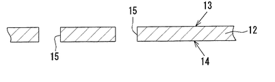
FIG. 1 schematically shows the laminated
[0034]
The thickness of the
[0035]
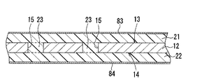
The buildup layer on the
[0036]
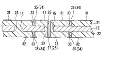
The first resin insulation layers 21 and 22 and the second resin insulation layers 41 and 42 have a thickness of 30 μm, and a resin-resin composite material in which continuous porous PTFE is impregnated with an epoxy resin. Consists of. The first resin insulation layers 21 and 22 are formed on the
[0037]
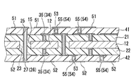
The first wiring layers 31 and 32 are both made of an Fe—Ni alloy having a thickness of about 15 μm, and are formed on the first resin insulation layers 21 and 22, respectively. A via
[0038]
The second wiring layers 51 and 52 are both made of an Fe—Ni alloy having a thickness of about 15 μm, and are formed on the second
[0039]
The third resin insulation layers 61 and 62 located at the outermost layer have a thickness of 20 μm and are formed on the second resin insulation layers 41 and 42 using a photosensitive epoxy resin. Yes. Via
[0040]
The first resin insulation layers 21 and 22 and the
[0041]
A so-called metal core package can be obtained by mounting an IC chip or the like (not shown) on such a laminated
[0042]
Next, a procedure for manufacturing the laminated
[0043]
First, a
[0044]
In this state, when the
[0045]
Subsequently, first resin insulation layers 21 and 22 and a
[0046]
Specifically, as shown in the table of FIG. 13, for the examples, metal foils 83 and 84 (namely, rolled 42 alloy foil, rolled 50 alloy foil, rolled amber) made of five types of Fe—Ni-based rolled alloys. Foil, rolled superamber foil, rolled Kovar foil). On the other hand, copper foil was used about the comparative example (namely, conventional example).
[0047]
Next, by carrying out laser drilling using a YAG laser or a carbon dioxide gas laser, the first resin insulation layers 21 and 22, the
[0048]
Next, a via
[0049]
Next, an epoxy resin is filled in the blind via-
[0050]
Next, by performing laser drilling using a YAG laser or a carbon dioxide laser, the first resin insulation layers 21 and 22, the second resin insulation layers 41 and 42, the
[0051]
Next, the via
[0052]
Next, the
[0053]
Next, on the third resin insulation layers 61 and 62, using an electroless Fe—Ni alloy plating, an etching process, an electroless nickel plating, and an electroless gold plating are sequentially performed using a conventionally known method. By applying,
[0054]
Therefore, according to the present embodiment, the following effects can be obtained.
[0055]
(1) In this laminated
[0056]
In the case of this laminated
[0057]
(2) Moreover, in the manufacturing method of this embodiment, laminated metal foils 83,84 The wiring layers 31, 32, 51, and 52 are formed by etching (that is, the subtractive method). Therefore, it is possible to manufacture the multilayer
[0058]
In addition, you may change embodiment of this invention as follows.
[0059]
In the above-described embodiment, all of the plurality of wiring layers 31, 32, 51, 52 are formed using the same metal material (Fe—Ni alloy). However, the present invention is not limited to this. For example, an Fe—Ni alloy may be used only for the wiring layers 31 and 32, and a metal material other than the Fe—Ni alloy having a lower thermal expansion coefficient than copper may be used for the wiring layers 51 and 52.
[0060]
The via-
[0061]
The present invention may be embodied in a form in which the via-hole conductor 34 (first via-hole conductor) that connects and conducts between the
[0062]
In the above embodiment, a specific example of the laminated
[0063]
In the above embodiment, the same number of
[0064]
In the above embodiment, the specific example of the laminated
[0065]
Next, in addition to the technical ideas described in the claims, the technical ideas grasped by the embodiment described above are listed below.
[0066]
(1) The difference between the thermal expansion coefficient of the conductive metal material constituting the wiring layer and the thermal expansion coefficient of the conductive metal material constituting the metal plate is 6 ppm / ° C. or less (preferably 2 ppm / ° C. or less, particularly 3. The laminated resin wiring board according to claim 1 or 2, which is preferably 1 ppm / ° C. or less.
[0067]
(2) The coefficient of thermal expansion of the conductive metal material constituting the wiring layer and the coefficient of thermal expansion of the conductive metal material constituting the metal plate are both less than 14 ppm / ° C. (preferably less than 11 ppm / ° C., particularly 3. The laminated resin wiring board according to claim 1 or 2, which is preferably less than 6 ppm / ° C.
[0068]
(3) The laminated resin wiring board according to claim 1 or 2, wherein the wiring layer and the metal plate are made of the same kind of metal.
[0069]
(4) The multilayer resin wiring board according to any one of claims 1 to 3, wherein the wiring layer is formed by etching a metal foil.
[0070]
(5) The laminated resin according to any one of claims 1 to 3, wherein the metal plate is a rolled metal plate, and the wiring layer is formed by etching a rolled metal foil. Wiring board.
[0071]
(6) The multilayer resin wiring board according to claim 2 or 3, wherein all of the plurality of wiring layers are made of an Fe-Ni alloy.
[0072]
(7) A via-hole conductor that connects and connects between the wiring layer and the metal plate or between the wiring layers is provided, and the via-hole conductor is formed by electroless plating of a conductive metal having a lower thermal expansion coefficient than copper. The laminated resin wiring board according to claim 1, wherein the laminated resin wiring board is formed.
[0073]
(8) A via hole conductor for connecting and connecting the wiring layer and the metal plate or between the wiring layers is provided, and the via hole conductor is formed by electroless Fe—Ni alloy plating. The laminated resin wiring board according to any one of claims 1 to 3.
[0074]
(9) A metal plate made of a rolled Fe—Ni alloy material having a first main surface and a second main surface and having a thickness of 150 μm or more, and a first main surface side and a second main surface side of the metal plate. , A plurality of wiring layers formed by etching a rolled Fe-Ni alloy foil, and a plurality of layers interposed between the metal plate and the wiring layer, or between the metal plate and the wiring layer and between the wiring layers. A resin insulating layer, a first via-hole conductor formed in the resin insulating layer and connected and connected between the wiring layer and the metal plate, and the first main surface and the second main surface of the metal plate A resin filler filled in a metal plate through-hole communicating with the metal plate, and a via hole forming hole penetrating the resin filler, and the first main surface side while maintaining insulation between the metal plate And a second via for connecting and connecting between the wiring layer and the wiring layer on the second main surface side Laminating resin wiring board, characterized in that a Lumpur conductor.
[Brief description of the drawings]
FIG. 1 is a schematic partial cross-sectional view showing a laminated resin wiring board according to an embodiment of the present invention.
FIG. 2 is a partial cross-sectional schematic view showing a metal plate that is a constituent member of the wiring board.
FIG. 3 is a partial cross-sectional schematic view showing a state in which a photoetching mask is formed on a metal plate.
FIG. 4 is a partial cross-sectional schematic view showing a state where metal plate through holes are formed by photoetching.
FIG. 5 is a partial cross-sectional schematic view showing a state in which a photoetching mask is removed.
FIG. 6 is a partial cross-sectional schematic view showing a state in which a first resin insulating layer and a metal foil are laminated.
FIG. 7 is a partial cross-sectional schematic view showing a state in which a hole for forming a via hole is formed in the first resin insulating layer.
FIG. 8 is a partial cross-sectional schematic view showing a state where a blind via-hole conductor is formed.
FIG. 9 is a partial cross-sectional schematic view showing a state in which a second resin insulating layer and a metal foil are laminated.
FIG. 10 is a partial cross-sectional schematic view showing a state in which a hole for forming a via hole is formed in a second resin insulating layer or the like.
FIG. 11 is a partial cross-sectional schematic view showing a state in which a blind via hole conductor and a metal plate insulating via hole conductor are formed.
FIG. 12 is a partial cross-sectional schematic view showing a state in which a third resin insulating layer is formed.
FIG. 13 is a table showing combinations of metal materials used for metal foils constituting a metal plate and a wiring layer for each example and comparative example.
[Explanation of symbols]
11 ... Laminated resin wiring board
12 ... Metal plate
13 ... Upper surface as the first main surface
14 ... lower surface which is the second main surface
21, 22, 41, 42, 61, 62 ... resin insulation layer
31, 32, 51, 52 ... wiring layer
83,84 ... metal foil
Claims (4)
前記圧延Fe−Ni合金板における前記第1主面及び前記第2主面のうちの少なくともいずれかの側に、樹脂絶縁層形成用材料を介して、前記圧延Fe−Ni系合金箔を積層する工程と、
積層された前記圧延Fe−Ni系合金箔をエッチングして前記配線層を形成する工程と、
前記無電解Fe−Ni合金めっきによって、前記樹脂絶縁層に形成されたビアホール形成用孔内に前記ビア導体を形成する工程と
を含むことを特徴とする積層樹脂配線基板の製造方法。A metal plate made of a rolled Fe-Ni alloy plate, which is a conductive metal material having a first main surface and a second main surface and having a lower thermal expansion coefficient than copper, the first main surface and the second main surface A wiring layer formed by etching a rolled Fe—Ni alloy foil, which is a conductive metal material having a thermal expansion coefficient lower than that of copper, located on at least one side of the metal plate, the metal plate, and the wiring A resin insulating layer interposed between the wiring layer and a via-hole conductor having a via conductor made of electroless Fe-Ni alloy plating and connected and conductive between the wiring layer and the metal plate; A method of manufacturing a laminated resin wiring substrate that can function as a ground layer or a power supply layer ,
The rolled Fe—Ni alloy foil is laminated on at least one of the first main surface and the second main surface of the rolled Fe—Ni alloy plate with a resin insulating layer forming material interposed therebetween. Process,
Etching the laminated rolled Fe-Ni alloy foil to form the wiring layer ;
Forming the via conductor in a hole for forming a via hole formed in the resin insulation layer by the electroless Fe-Ni alloy plating;
The manufacturing method of the laminated resin wiring board characterized by including.
Priority Applications (1)
| Application Number | Priority Date | Filing Date | Title |
|---|---|---|---|
| JP2002187256A JP4061137B2 (en) | 2002-06-27 | 2002-06-27 | Multilayer resin wiring board and manufacturing method thereof |
Applications Claiming Priority (1)
| Application Number | Priority Date | Filing Date | Title |
|---|---|---|---|
| JP2002187256A JP4061137B2 (en) | 2002-06-27 | 2002-06-27 | Multilayer resin wiring board and manufacturing method thereof |
Publications (3)
| Publication Number | Publication Date |
|---|---|
| JP2004031731A JP2004031731A (en) | 2004-01-29 |
| JP2004031731A5 JP2004031731A5 (en) | 2005-06-02 |
| JP4061137B2 true JP4061137B2 (en) | 2008-03-12 |
Family
ID=31182344
Family Applications (1)
| Application Number | Title | Priority Date | Filing Date |
|---|---|---|---|
| JP2002187256A Expired - Fee Related JP4061137B2 (en) | 2002-06-27 | 2002-06-27 | Multilayer resin wiring board and manufacturing method thereof |
Country Status (1)
| Country | Link |
|---|---|
| JP (1) | JP4061137B2 (en) |
Families Citing this family (9)
| Publication number | Priority date | Publication date | Assignee | Title |
|---|---|---|---|---|
| KR100885900B1 (en) * | 2007-08-24 | 2009-02-26 | 삼성전기주식회사 | Multilayered printed circuit board and fabricating method therefof |
| JP5217639B2 (en) | 2008-05-30 | 2013-06-19 | 富士通株式会社 | Core substrate and printed wiring board |
| JP2009290124A (en) | 2008-05-30 | 2009-12-10 | Fujitsu Ltd | Printed wiring board |
| JP5217640B2 (en) | 2008-05-30 | 2013-06-19 | 富士通株式会社 | Method for manufacturing printed wiring board and method for manufacturing printed circuit board unit |
| KR101411584B1 (en) * | 2013-04-12 | 2014-06-24 | 김영대 | method for manufacturing battery protection apparatus and the battery protection apparatus |
| KR102288666B1 (en) | 2013-12-27 | 2021-08-11 | 미쓰이금속광업주식회사 | Composite metal foil, composite metal foil with carrier, metal-clad laminate obtained using said composite metal foil or said composite metal foil with carrier, and printed wiring board |
| JP7381323B2 (en) * | 2019-12-17 | 2023-11-15 | 日東電工株式会社 | Method for manufacturing double-sided printed circuit board and double-sided printed circuit board |
| CN113613390A (en) * | 2021-07-28 | 2021-11-05 | 深圳市普林电路有限公司 | Selective vacuum resin hole plugging process |
| CN113693878A (en) * | 2021-08-17 | 2021-11-26 | 迈族智能科技(上海)有限公司 | Vertical vibration amplitude auxiliary platform |
-
2002
- 2002-06-27 JP JP2002187256A patent/JP4061137B2/en not_active Expired - Fee Related
Also Published As
| Publication number | Publication date |
|---|---|
| JP2004031731A (en) | 2004-01-29 |
Similar Documents
| Publication | Publication Date | Title |
|---|---|---|
| JP3956204B2 (en) | MULTILAYER RESIN WIRING BOARD AND METHOD FOR MANUFACTURING THE SAME, METAL PLATE FOR LAMINATED RESIN WIRING BOARD | |
| TW201101955A (en) | Multilayer printed wiring board | |
| JP4008782B2 (en) | Manufacturing method of multilayer wiring board | |
| JP4592891B2 (en) | Multilayer circuit board and semiconductor device | |
| JP3215090B2 (en) | Wiring board, multilayer wiring board, and methods of manufacturing the same | |
| JP3492467B2 (en) | Single-sided circuit board for multilayer printed wiring board, multilayer printed wiring board and method of manufacturing the same | |
| JP4061137B2 (en) | Multilayer resin wiring board and manufacturing method thereof | |
| JP2002076637A (en) | Substrate incorporating chip component, and manufacturing method of the substrate | |
| JP3953900B2 (en) | Multilayer resin wiring board and manufacturing method thereof | |
| JP4521223B2 (en) | Printed wiring board | |
| JP2007115809A (en) | Wiring board | |
| JP2005038918A (en) | Multilayer flexible printed wiring board and its production | |
| KR101109287B1 (en) | Printed circuit board with electronic components embedded therein and method for fabricating the same | |
| JP3914102B2 (en) | Manufacturing method of laminated resin wiring board | |
| JP2005072085A (en) | Method of manufacturing wiring board and wiring board | |
| KR101109277B1 (en) | Fabricating Method of Printed Circuit Board | |
| JP3961909B2 (en) | Multilayer printed circuit board | |
| KR20100095742A (en) | Manufacturing method for embedded pcb, and embedded pcb structure using the same | |
| CN114342574A (en) | Circuit board, method for manufacturing circuit board, and electronic apparatus | |
| JP3955799B2 (en) | Wiring board manufacturing method | |
| JP2004111578A (en) | Process for producing build-up printed wiring board with heat spreader and build-up printed wiring board with heat spreader | |
| JP2007235176A (en) | Multilayer interconnection board, and semiconductor device using same | |
| JP3253886B2 (en) | Single-sided circuit board for multilayer printed wiring board, method for manufacturing the same, and multilayer printed wiring board | |
| JP2004214271A (en) | Single side lamination wiring board and its manufacturing method | |
| KR20100132358A (en) | Manufacturing method of a build-up printed circuit board with via-holes of stack type using bump structure |
Legal Events
| Date | Code | Title | Description |
|---|---|---|---|
| A521 | Written amendment |
Free format text: JAPANESE INTERMEDIATE CODE: A523 Effective date: 20040817 |
|
| A621 | Written request for application examination |
Free format text: JAPANESE INTERMEDIATE CODE: A621 Effective date: 20040817 |
|
| A131 | Notification of reasons for refusal |
Free format text: JAPANESE INTERMEDIATE CODE: A131 Effective date: 20070515 |
|
| A521 | Written amendment |
Free format text: JAPANESE INTERMEDIATE CODE: A523 Effective date: 20070707 |
|
| A02 | Decision of refusal |
Free format text: JAPANESE INTERMEDIATE CODE: A02 Effective date: 20070731 |
|
| A521 | Written amendment |
Free format text: JAPANESE INTERMEDIATE CODE: A523 Effective date: 20070927 |
|
| A911 | Transfer of reconsideration by examiner before appeal (zenchi) |
Free format text: JAPANESE INTERMEDIATE CODE: A911 Effective date: 20071029 |
|
| TRDD | Decision of grant or rejection written | ||
| A01 | Written decision to grant a patent or to grant a registration (utility model) |
Free format text: JAPANESE INTERMEDIATE CODE: A01 Effective date: 20071129 |
|
| A61 | First payment of annual fees (during grant procedure) |
Free format text: JAPANESE INTERMEDIATE CODE: A61 Effective date: 20071221 |
|
| FPAY | Renewal fee payment (event date is renewal date of database) |
Free format text: PAYMENT UNTIL: 20101228 Year of fee payment: 3 |
|
| R150 | Certificate of patent or registration of utility model |
Free format text: JAPANESE INTERMEDIATE CODE: R150 |
|
| FPAY | Renewal fee payment (event date is renewal date of database) |
Free format text: PAYMENT UNTIL: 20101228 Year of fee payment: 3 |
|
| FPAY | Renewal fee payment (event date is renewal date of database) |
Free format text: PAYMENT UNTIL: 20101228 Year of fee payment: 3 |
|
| FPAY | Renewal fee payment (event date is renewal date of database) |
Free format text: PAYMENT UNTIL: 20111228 Year of fee payment: 4 |
|
| FPAY | Renewal fee payment (event date is renewal date of database) |
Free format text: PAYMENT UNTIL: 20111228 Year of fee payment: 4 |
|
| FPAY | Renewal fee payment (event date is renewal date of database) |
Free format text: PAYMENT UNTIL: 20121228 Year of fee payment: 5 |
|
| FPAY | Renewal fee payment (event date is renewal date of database) |
Free format text: PAYMENT UNTIL: 20121228 Year of fee payment: 5 |
|
| FPAY | Renewal fee payment (event date is renewal date of database) |
Free format text: PAYMENT UNTIL: 20131228 Year of fee payment: 6 |
|
| LAPS | Cancellation because of no payment of annual fees |