JP5114773B2 - 表面実装型発光装置 - Google Patents
表面実装型発光装置 Download PDFInfo
- Publication number
- JP5114773B2 JP5114773B2 JP2007209973A JP2007209973A JP5114773B2 JP 5114773 B2 JP5114773 B2 JP 5114773B2 JP 2007209973 A JP2007209973 A JP 2007209973A JP 2007209973 A JP2007209973 A JP 2007209973A JP 5114773 B2 JP5114773 B2 JP 5114773B2
- Authority
- JP
- Japan
- Prior art keywords
- light emitting
- peeling
- light
- interface
- emitting element
- Prior art date
- Legal status (The legal status is an assumption and is not a legal conclusion. Google has not performed a legal analysis and makes no representation as to the accuracy of the status listed.)
- Expired - Fee Related
Links
Images


Classifications
-
- H—ELECTRICITY
- H10—SEMICONDUCTOR DEVICES; ELECTRIC SOLID-STATE DEVICES NOT OTHERWISE PROVIDED FOR
- H10H—INORGANIC LIGHT-EMITTING SEMICONDUCTOR DEVICES HAVING POTENTIAL BARRIERS
- H10H20/00—Individual inorganic light-emitting semiconductor devices having potential barriers, e.g. light-emitting diodes [LED]
- H10H20/80—Constructional details
- H10H20/85—Packages
- H10H20/857—Interconnections, e.g. lead-frames, bond wires or solder balls
-
- H—ELECTRICITY
- H01—ELECTRIC ELEMENTS
- H01L—SEMICONDUCTOR DEVICES NOT COVERED BY CLASS H10
- H01L2224/00—Indexing scheme for arrangements for connecting or disconnecting semiconductor or solid-state bodies and methods related thereto as covered by H01L24/00
- H01L2224/01—Means for bonding being attached to, or being formed on, the surface to be connected, e.g. chip-to-package, die-attach, "first-level" interconnects; Manufacturing methods related thereto
- H01L2224/42—Wire connectors; Manufacturing methods related thereto
- H01L2224/47—Structure, shape, material or disposition of the wire connectors after the connecting process
- H01L2224/48—Structure, shape, material or disposition of the wire connectors after the connecting process of an individual wire connector
- H01L2224/4805—Shape
- H01L2224/4809—Loop shape
- H01L2224/48091—Arched
-
- H—ELECTRICITY
- H01—ELECTRIC ELEMENTS
- H01L—SEMICONDUCTOR DEVICES NOT COVERED BY CLASS H10
- H01L2224/00—Indexing scheme for arrangements for connecting or disconnecting semiconductor or solid-state bodies and methods related thereto as covered by H01L24/00
- H01L2224/01—Means for bonding being attached to, or being formed on, the surface to be connected, e.g. chip-to-package, die-attach, "first-level" interconnects; Manufacturing methods related thereto
- H01L2224/42—Wire connectors; Manufacturing methods related thereto
- H01L2224/47—Structure, shape, material or disposition of the wire connectors after the connecting process
- H01L2224/48—Structure, shape, material or disposition of the wire connectors after the connecting process of an individual wire connector
- H01L2224/481—Disposition
- H01L2224/48151—Connecting between a semiconductor or solid-state body and an item not being a semiconductor or solid-state body, e.g. chip-to-substrate, chip-to-passive
- H01L2224/48221—Connecting between a semiconductor or solid-state body and an item not being a semiconductor or solid-state body, e.g. chip-to-substrate, chip-to-passive the body and the item being stacked
- H01L2224/48225—Connecting between a semiconductor or solid-state body and an item not being a semiconductor or solid-state body, e.g. chip-to-substrate, chip-to-passive the body and the item being stacked the item being non-metallic, e.g. insulating substrate with or without metallisation
- H01L2224/48227—Connecting between a semiconductor or solid-state body and an item not being a semiconductor or solid-state body, e.g. chip-to-substrate, chip-to-passive the body and the item being stacked the item being non-metallic, e.g. insulating substrate with or without metallisation connecting the wire to a bond pad of the item
-
- H—ELECTRICITY
- H10—SEMICONDUCTOR DEVICES; ELECTRIC SOLID-STATE DEVICES NOT OTHERWISE PROVIDED FOR
- H10H—INORGANIC LIGHT-EMITTING SEMICONDUCTOR DEVICES HAVING POTENTIAL BARRIERS
- H10H20/00—Individual inorganic light-emitting semiconductor devices having potential barriers, e.g. light-emitting diodes [LED]
- H10H20/80—Constructional details
- H10H20/85—Packages
- H10H20/852—Encapsulations
Landscapes
- Led Device Packages (AREA)
Description
(第1の実施の形態)
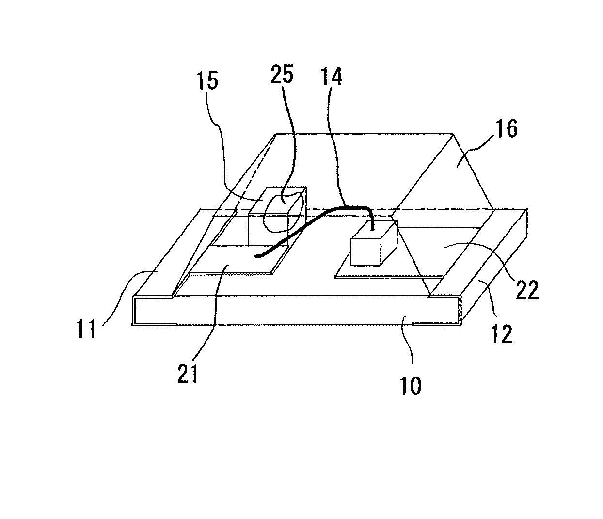
本実施の形態の表面実装型LEDの構造を図1を用いて説明する。(ただし、図1では、封止樹脂16内部に配置された物の形状を明確に示すため、樹脂16内の物の外形を実線で描いている。)図1のように、表面実装型LEDは、基板10と、基板10の上面に配置された一対の回路パターン11,12と、LEDチップ13とを有している。回路パターン12は、基板10の上面にチップ搭載領域22を備え、LEDチップ13は、この領域に搭載されている。回路パターン11は、基板10の上面に、ボンディング領域21と、他の部分よりも厚く形成された厚膜金属層部15とを備えている。厚膜金属層部15の詳しい構成および作用については後述する。回路パターン11、12はそれぞれ、基板10の上面のみならず、側面を通って裏面に回り込むように形成され、基板10の裏面側から給電可能な構成になっている。
第2の実施の形態の表面実装型LEDは、第1の実施の形態の厚膜金属層部15に代えて、LEDチップ13と封止樹脂16との界面よりも先に界面剥離を引き起こすための剥離誘起構造体として、半導体製のダミー構造物を搭載する。半導体製のダミー構造物の搭載位置は、厚膜金属層部15と同様である。ただし、半導体製のダミー構造物は、同じ半導体のLEDチップ13と熱膨張率が同程度であるため、その高さが、LEDチップ13よりも大きいものを用いる。また、半導体製ダミー構造物は、上面積と側面積の和が、LEDチップ13よりも大きいことが望ましい。
Claims (5)
- 基板と、基板上に配置された一対の回路パターンと、発光素子と、該発光素子を封止する樹脂とを有し、
前記一対の回路パターンのうち一方は、前記発光素子を搭載する素子搭載領域を備え、他方は、前記発光素子にワイヤにより接続されるワイヤ接続領域を備え、
前記基板上には、前記発光素子と樹脂との界面よりも先に界面剥離を引き起こすための剥離誘起構造体が配置され、
該剥離誘起構造体として、前記一対の回路パターンには、前記素子搭載領域および前記ワイヤ接続領域のうち厚い方の膜厚の1.6倍以上の厚さを有し、金属材料から成る厚膜部が設けられていることを特徴とする表面実装型発光装置。 - 請求項1に記載の表面実装型発光装置において、前記厚膜部の外形は、角部を有する形状であることを特徴とする表面実装型発光装置。
- 請求項1または2に記載の表面実装型発光装置において、前記厚膜部は、前記素子搭載領域および前記ワイヤ接続領域のうち厚い方の膜厚の2倍以上の厚さを有することを特徴とする表面実装型発光装置。
- 請求項1または2に記載の表面実装型発光装置において、前記厚膜部は、前記発光素子の高さ以上の厚さを有することを特徴とする表面実装型発光装置。
- 請求項1に記載の表面実装型発光装置において、前記剥離誘起構造体は、当該剥離誘起構造体と前記樹脂との界面より生じた界面剥離が前記発光素子から発せられた光に影響を与えないようにするために、前記発光素子から離れた位置に配置されていることを特徴とする表面実装型発光装置。
Priority Applications (2)
| Application Number | Priority Date | Filing Date | Title |
|---|---|---|---|
| JP2007209973A JP5114773B2 (ja) | 2007-08-10 | 2007-08-10 | 表面実装型発光装置 |
| US12/187,597 US7750361B2 (en) | 2007-08-10 | 2008-08-07 | Surface mount light emitting apparatus |
Applications Claiming Priority (1)
| Application Number | Priority Date | Filing Date | Title |
|---|---|---|---|
| JP2007209973A JP5114773B2 (ja) | 2007-08-10 | 2007-08-10 | 表面実装型発光装置 |
Publications (2)
| Publication Number | Publication Date |
|---|---|
| JP2009044082A JP2009044082A (ja) | 2009-02-26 |
| JP5114773B2 true JP5114773B2 (ja) | 2013-01-09 |
Family
ID=40430874
Family Applications (1)
| Application Number | Title | Priority Date | Filing Date |
|---|---|---|---|
| JP2007209973A Expired - Fee Related JP5114773B2 (ja) | 2007-08-10 | 2007-08-10 | 表面実装型発光装置 |
Country Status (2)
| Country | Link |
|---|---|
| US (1) | US7750361B2 (ja) |
| JP (1) | JP5114773B2 (ja) |
Families Citing this family (5)
| Publication number | Priority date | Publication date | Assignee | Title |
|---|---|---|---|---|
| USD609653S1 (en) * | 2008-10-07 | 2010-02-09 | Kabushiki Kaisha Toshiba | Light receiving and emitting device |
| JP2014135471A (ja) * | 2012-12-10 | 2014-07-24 | Nitto Denko Corp | 発光装置、発光装置集合体および電極付基板 |
| USD753612S1 (en) * | 2012-09-07 | 2016-04-12 | Cree, Inc. | Light emitter device |
| USD847102S1 (en) | 2013-02-08 | 2019-04-30 | Epistar Corporation | Light emitting diode |
| TWD161897S (zh) * | 2013-02-08 | 2014-07-21 | 晶元光電股份有限公司 | 發光二極體之部分 |
Family Cites Families (27)
| Publication number | Priority date | Publication date | Assignee | Title |
|---|---|---|---|---|
| JP3672280B2 (ja) * | 1996-10-29 | 2005-07-20 | 株式会社シチズン電子 | スルーホール電極付き電子部品の製造方法 |
| JP3673621B2 (ja) * | 1997-07-30 | 2005-07-20 | ローム株式会社 | チップ型発光素子 |
| JPH1146018A (ja) * | 1997-07-28 | 1999-02-16 | Citizen Electron Co Ltd | 表面実装型発光ダイオード |
| JP4174858B2 (ja) * | 1998-07-06 | 2008-11-05 | 日亜化学工業株式会社 | 発光ダイオード |
| JP2000124506A (ja) * | 1998-10-15 | 2000-04-28 | Rohm Co Ltd | 半導体発光素子 |
| JP2000188425A (ja) * | 1998-12-22 | 2000-07-04 | Nichia Chem Ind Ltd | 発光ダイオード |
| JP2001036140A (ja) * | 1999-07-16 | 2001-02-09 | Stanley Electric Co Ltd | 静電対策表面実装型led |
| JP2002124703A (ja) * | 2000-08-09 | 2002-04-26 | Rohm Co Ltd | チップ型発光装置 |
| JP4097949B2 (ja) * | 2001-04-20 | 2008-06-11 | シャープ株式会社 | 空間光伝送システム |
| JP4045781B2 (ja) * | 2001-08-28 | 2008-02-13 | 松下電工株式会社 | 発光装置 |
| JP4211359B2 (ja) * | 2002-03-06 | 2009-01-21 | 日亜化学工業株式会社 | 半導体装置の製造方法 |
| JP4085899B2 (ja) * | 2003-06-30 | 2008-05-14 | 日立エーアイシー株式会社 | 発光デバイス用基板および発光デバイス |
| JP4282392B2 (ja) * | 2003-07-11 | 2009-06-17 | 株式会社東芝 | 光半導体装置及びその製造方法 |
| JP4788109B2 (ja) * | 2003-10-28 | 2011-10-05 | パナソニック電工株式会社 | 半導体発光装置及びその製造方法 |
| JP2005197329A (ja) * | 2004-01-05 | 2005-07-21 | Stanley Electric Co Ltd | 表面実装型半導体装置及びそのリードフレーム構造 |
| JP2005347401A (ja) * | 2004-06-01 | 2005-12-15 | Meiko:Kk | 光素子チップ部品 |
| JP4359195B2 (ja) * | 2004-06-11 | 2009-11-04 | 株式会社東芝 | 半導体発光装置及びその製造方法並びに半導体発光ユニット |
| JP2006093672A (ja) * | 2004-08-26 | 2006-04-06 | Toshiba Corp | 半導体発光装置 |
| WO2006059828A1 (en) * | 2004-09-10 | 2006-06-08 | Seoul Semiconductor Co., Ltd. | Light emitting diode package having multiple molding resins |
| JP4626258B2 (ja) * | 2004-10-18 | 2011-02-02 | 日亜化学工業株式会社 | 発光ダイオード |
| JP2006190888A (ja) | 2005-01-07 | 2006-07-20 | Stanley Electric Co Ltd | 表面実装型led |
| JP4711715B2 (ja) * | 2005-03-30 | 2011-06-29 | 株式会社東芝 | 半導体発光装置及び半導体発光ユニット |
| TW200717866A (en) * | 2005-07-29 | 2007-05-01 | Toshiba Kk | Semiconductor light emitting device |
| JP4835104B2 (ja) * | 2005-10-24 | 2011-12-14 | 日亜化学工業株式会社 | 半導体発光装置 |
| JP2007142044A (ja) * | 2005-11-16 | 2007-06-07 | Stanley Electric Co Ltd | 半導体発光装置及びそれを用いた面光源 |
| JP2007212915A (ja) * | 2006-02-13 | 2007-08-23 | Seiko Epson Corp | 光電気複合基板及び電子機器 |
| TWM302123U (en) * | 2006-06-13 | 2006-12-01 | Lighthouse Technology Co Ltd | The stand structure of light-emitting diode |
-
2007
- 2007-08-10 JP JP2007209973A patent/JP5114773B2/ja not_active Expired - Fee Related
-
2008
- 2008-08-07 US US12/187,597 patent/US7750361B2/en not_active Expired - Fee Related
Also Published As
| Publication number | Publication date |
|---|---|
| US7750361B2 (en) | 2010-07-06 |
| US20090065796A1 (en) | 2009-03-12 |
| JP2009044082A (ja) | 2009-02-26 |
Similar Documents
| Publication | Publication Date | Title |
|---|---|---|
| JP5340583B2 (ja) | 半導体発光装置 | |
| KR101044200B1 (ko) | 리지드-플렉서블 회로기판 및 그 제조방법 | |
| KR102332362B1 (ko) | 초박형 임베디드 반도체 소자 패키지 및 그 제조 방법 | |
| JP4516320B2 (ja) | Led基板 | |
| JP6502205B2 (ja) | 多層配線基板およびその製造方法 | |
| JPWO2007116544A1 (ja) | 複合基板及び複合基板の製造方法 | |
| JP5114773B2 (ja) | 表面実装型発光装置 | |
| JPWO2007110985A1 (ja) | 複合基板及び複合基板の製造方法 | |
| JP2020161697A (ja) | 半導体発光装置 | |
| JPWO2007132612A1 (ja) | 複合基板及びその製造方法 | |
| JP2015192095A (ja) | Led発光装置及びled発光装置の製造方法 | |
| JP5691573B2 (ja) | モジュール部品の製造方法 | |
| CN103124468A (zh) | 金属基覆铜层压板和使用其制造金属芯印刷电路板的方法 | |
| JP2011100793A5 (ja) | 半導体パッケージ及びその製造方法 | |
| CN100499187C (zh) | 发光二极管 | |
| JP2008091814A (ja) | 回路基板及び回路基板の製造方法 | |
| JP2002222998A (ja) | 光半導体素子 | |
| JPWO2017014127A1 (ja) | Led搭載基板 | |
| KR101842938B1 (ko) | 캐비티기판 제조방법 | |
| JP2016100352A (ja) | プリント配線板およびその製造方法 | |
| JPWO2015118951A1 (ja) | 樹脂多層基板および部品モジュール | |
| WO2012165111A1 (ja) | 多層基板の製造方法および多層基板 | |
| JP2011003818A (ja) | モールドパッケージ | |
| WO2013145390A1 (ja) | フレキシブルプリント配線板およびその製造方法 | |
| JP5269468B2 (ja) | 半導体発光装置 |
Legal Events
| Date | Code | Title | Description |
|---|---|---|---|
| A621 | Written request for application examination |
Free format text: JAPANESE INTERMEDIATE CODE: A621 Effective date: 20100719 |
|
| A131 | Notification of reasons for refusal |
Free format text: JAPANESE INTERMEDIATE CODE: A131 Effective date: 20120228 |
|
| A977 | Report on retrieval |
Free format text: JAPANESE INTERMEDIATE CODE: A971007 Effective date: 20120229 |
|
| A521 | Request for written amendment filed |
Free format text: JAPANESE INTERMEDIATE CODE: A523 Effective date: 20120427 |
|
| A131 | Notification of reasons for refusal |
Free format text: JAPANESE INTERMEDIATE CODE: A131 Effective date: 20120626 |
|
| A521 | Request for written amendment filed |
Free format text: JAPANESE INTERMEDIATE CODE: A523 Effective date: 20120822 |
|
| TRDD | Decision of grant or rejection written | ||
| A01 | Written decision to grant a patent or to grant a registration (utility model) |
Free format text: JAPANESE INTERMEDIATE CODE: A01 Effective date: 20120918 |
|
| A01 | Written decision to grant a patent or to grant a registration (utility model) |
Free format text: JAPANESE INTERMEDIATE CODE: A01 |
|
| A61 | First payment of annual fees (during grant procedure) |
Free format text: JAPANESE INTERMEDIATE CODE: A61 Effective date: 20120925 |
|
| R150 | Certificate of patent or registration of utility model |
Ref document number: 5114773 Country of ref document: JP Free format text: JAPANESE INTERMEDIATE CODE: R150 Free format text: JAPANESE INTERMEDIATE CODE: R150 |
|
| FPAY | Renewal fee payment (event date is renewal date of database) |
Free format text: PAYMENT UNTIL: 20151026 Year of fee payment: 3 |
|
| R250 | Receipt of annual fees |
Free format text: JAPANESE INTERMEDIATE CODE: R250 |
|
| R250 | Receipt of annual fees |
Free format text: JAPANESE INTERMEDIATE CODE: R250 |
|
| R250 | Receipt of annual fees |
Free format text: JAPANESE INTERMEDIATE CODE: R250 |
|
| R250 | Receipt of annual fees |
Free format text: JAPANESE INTERMEDIATE CODE: R250 |
|
| R250 | Receipt of annual fees |
Free format text: JAPANESE INTERMEDIATE CODE: R250 |
|
| R250 | Receipt of annual fees |
Free format text: JAPANESE INTERMEDIATE CODE: R250 |
|
| R250 | Receipt of annual fees |
Free format text: JAPANESE INTERMEDIATE CODE: R250 |
|
| R250 | Receipt of annual fees |
Free format text: JAPANESE INTERMEDIATE CODE: R250 |
|
| LAPS | Cancellation because of no payment of annual fees |