JP4981712B2 - 配線基板の製造方法及び半導体パッケージの製造方法 - Google Patents
配線基板の製造方法及び半導体パッケージの製造方法 Download PDFInfo
- Publication number
- JP4981712B2 JP4981712B2 JP2008050910A JP2008050910A JP4981712B2 JP 4981712 B2 JP4981712 B2 JP 4981712B2 JP 2008050910 A JP2008050910 A JP 2008050910A JP 2008050910 A JP2008050910 A JP 2008050910A JP 4981712 B2 JP4981712 B2 JP 4981712B2
- Authority
- JP
- Japan
- Prior art keywords
- layer
- wiring
- wiring board
- semiconductor chip
- substrate
- Prior art date
- Legal status (The legal status is an assumption and is not a legal conclusion. Google has not performed a legal analysis and makes no representation as to the accuracy of the status listed.)
- Active
Links
Images


Classifications
-
- H—ELECTRICITY
- H05—ELECTRIC TECHNIQUES NOT OTHERWISE PROVIDED FOR
- H05K—PRINTED CIRCUITS; CASINGS OR CONSTRUCTIONAL DETAILS OF ELECTRIC APPARATUS; MANUFACTURE OF ASSEMBLAGES OF ELECTRICAL COMPONENTS
- H05K3/00—Apparatus or processes for manufacturing printed circuits
- H05K3/30—Assembling printed circuits with electric components, e.g. with resistor
- H05K3/32—Assembling printed circuits with electric components, e.g. with resistor electrically connecting electric components or wires to printed circuits
- H05K3/34—Assembling printed circuits with electric components, e.g. with resistor electrically connecting electric components or wires to printed circuits by soldering
- H05K3/3457—Solder materials or compositions; Methods of application thereof
- H05K3/3473—Plating of solder
-
- H—ELECTRICITY
- H01—ELECTRIC ELEMENTS
- H01L—SEMICONDUCTOR DEVICES NOT COVERED BY CLASS H10
- H01L21/00—Processes or apparatus adapted for the manufacture or treatment of semiconductor or solid state devices or of parts thereof
- H01L21/02—Manufacture or treatment of semiconductor devices or of parts thereof
- H01L21/04—Manufacture or treatment of semiconductor devices or of parts thereof the devices having at least one potential-jump barrier or surface barrier, e.g. PN junction, depletion layer or carrier concentration layer
- H01L21/48—Manufacture or treatment of parts, e.g. containers, prior to assembly of the devices, using processes not provided for in a single one of the subgroups H01L21/06 - H01L21/326
- H01L21/4814—Conductive parts
- H01L21/4846—Leads on or in insulating or insulated substrates, e.g. metallisation
- H01L21/4857—Multilayer substrates
-
- H—ELECTRICITY
- H01—ELECTRIC ELEMENTS
- H01L—SEMICONDUCTOR DEVICES NOT COVERED BY CLASS H10
- H01L21/00—Processes or apparatus adapted for the manufacture or treatment of semiconductor or solid state devices or of parts thereof
- H01L21/02—Manufacture or treatment of semiconductor devices or of parts thereof
- H01L21/04—Manufacture or treatment of semiconductor devices or of parts thereof the devices having at least one potential-jump barrier or surface barrier, e.g. PN junction, depletion layer or carrier concentration layer
- H01L21/50—Assembly of semiconductor devices using processes or apparatus not provided for in a single one of the subgroups H01L21/06 - H01L21/326, e.g. sealing of a cap to a base of a container
- H01L21/56—Encapsulations, e.g. encapsulation layers, coatings
- H01L21/568—Temporary substrate used as encapsulation process aid
-
- H—ELECTRICITY
- H01—ELECTRIC ELEMENTS
- H01L—SEMICONDUCTOR DEVICES NOT COVERED BY CLASS H10
- H01L21/00—Processes or apparatus adapted for the manufacture or treatment of semiconductor or solid state devices or of parts thereof
- H01L21/67—Apparatus specially adapted for handling semiconductor or electric solid state devices during manufacture or treatment thereof; Apparatus specially adapted for handling wafers during manufacture or treatment of semiconductor or electric solid state devices or components ; Apparatus not specifically provided for elsewhere
- H01L21/683—Apparatus specially adapted for handling semiconductor or electric solid state devices during manufacture or treatment thereof; Apparatus specially adapted for handling wafers during manufacture or treatment of semiconductor or electric solid state devices or components ; Apparatus not specifically provided for elsewhere for supporting or gripping
- H01L21/6835—Apparatus specially adapted for handling semiconductor or electric solid state devices during manufacture or treatment thereof; Apparatus specially adapted for handling wafers during manufacture or treatment of semiconductor or electric solid state devices or components ; Apparatus not specifically provided for elsewhere for supporting or gripping using temporarily an auxiliary support
-
- H—ELECTRICITY
- H01—ELECTRIC ELEMENTS
- H01L—SEMICONDUCTOR DEVICES NOT COVERED BY CLASS H10
- H01L24/00—Arrangements for connecting or disconnecting semiconductor or solid-state bodies; Methods or apparatus related thereto
- H01L24/80—Methods for connecting semiconductor or other solid state bodies using means for bonding being attached to, or being formed on, the surface to be connected
- H01L24/81—Methods for connecting semiconductor or other solid state bodies using means for bonding being attached to, or being formed on, the surface to be connected using a bump connector
-
- H—ELECTRICITY
- H01—ELECTRIC ELEMENTS
- H01L—SEMICONDUCTOR DEVICES NOT COVERED BY CLASS H10
- H01L24/00—Arrangements for connecting or disconnecting semiconductor or solid-state bodies; Methods or apparatus related thereto
- H01L24/93—Batch processes
- H01L24/95—Batch processes at chip-level, i.e. with connecting carried out on a plurality of singulated devices, i.e. on diced chips
- H01L24/97—Batch processes at chip-level, i.e. with connecting carried out on a plurality of singulated devices, i.e. on diced chips the devices being connected to a common substrate, e.g. interposer, said common substrate being separable into individual assemblies after connecting
-
- H—ELECTRICITY
- H05—ELECTRIC TECHNIQUES NOT OTHERWISE PROVIDED FOR
- H05K—PRINTED CIRCUITS; CASINGS OR CONSTRUCTIONAL DETAILS OF ELECTRIC APPARATUS; MANUFACTURE OF ASSEMBLAGES OF ELECTRICAL COMPONENTS
- H05K3/00—Apparatus or processes for manufacturing printed circuits
- H05K3/46—Manufacturing multilayer circuits
- H05K3/4644—Manufacturing multilayer circuits by building the multilayer layer by layer, i.e. build-up multilayer circuits
- H05K3/4682—Manufacture of core-less build-up multilayer circuits on a temporary carrier or on a metal foil
-
- H—ELECTRICITY
- H01—ELECTRIC ELEMENTS
- H01L—SEMICONDUCTOR DEVICES NOT COVERED BY CLASS H10
- H01L2221/00—Processes or apparatus adapted for the manufacture or treatment of semiconductor or solid state devices or of parts thereof covered by H01L21/00
- H01L2221/67—Apparatus for handling semiconductor or electric solid state devices during manufacture or treatment thereof; Apparatus for handling wafers during manufacture or treatment of semiconductor or electric solid state devices or components; Apparatus not specifically provided for elsewhere
- H01L2221/683—Apparatus for handling semiconductor or electric solid state devices during manufacture or treatment thereof; Apparatus for handling wafers during manufacture or treatment of semiconductor or electric solid state devices or components; Apparatus not specifically provided for elsewhere for supporting or gripping
- H01L2221/68304—Apparatus for handling semiconductor or electric solid state devices during manufacture or treatment thereof; Apparatus for handling wafers during manufacture or treatment of semiconductor or electric solid state devices or components; Apparatus not specifically provided for elsewhere for supporting or gripping using temporarily an auxiliary support
- H01L2221/68345—Apparatus for handling semiconductor or electric solid state devices during manufacture or treatment thereof; Apparatus for handling wafers during manufacture or treatment of semiconductor or electric solid state devices or components; Apparatus not specifically provided for elsewhere for supporting or gripping using temporarily an auxiliary support used as a support during the manufacture of self supporting substrates
-
- H—ELECTRICITY
- H01—ELECTRIC ELEMENTS
- H01L—SEMICONDUCTOR DEVICES NOT COVERED BY CLASS H10
- H01L2224/00—Indexing scheme for arrangements for connecting or disconnecting semiconductor or solid-state bodies and methods related thereto as covered by H01L24/00
- H01L2224/01—Means for bonding being attached to, or being formed on, the surface to be connected, e.g. chip-to-package, die-attach, "first-level" interconnects; Manufacturing methods related thereto
- H01L2224/10—Bump connectors; Manufacturing methods related thereto
- H01L2224/15—Structure, shape, material or disposition of the bump connectors after the connecting process
- H01L2224/16—Structure, shape, material or disposition of the bump connectors after the connecting process of an individual bump connector
- H01L2224/161—Disposition
- H01L2224/16151—Disposition the bump connector connecting between a semiconductor or solid-state body and an item not being a semiconductor or solid-state body, e.g. chip-to-substrate, chip-to-passive
- H01L2224/16221—Disposition the bump connector connecting between a semiconductor or solid-state body and an item not being a semiconductor or solid-state body, e.g. chip-to-substrate, chip-to-passive the body and the item being stacked
- H01L2224/16225—Disposition the bump connector connecting between a semiconductor or solid-state body and an item not being a semiconductor or solid-state body, e.g. chip-to-substrate, chip-to-passive the body and the item being stacked the item being non-metallic, e.g. insulating substrate with or without metallisation
-
- H—ELECTRICITY
- H01—ELECTRIC ELEMENTS
- H01L—SEMICONDUCTOR DEVICES NOT COVERED BY CLASS H10
- H01L2224/00—Indexing scheme for arrangements for connecting or disconnecting semiconductor or solid-state bodies and methods related thereto as covered by H01L24/00
- H01L2224/01—Means for bonding being attached to, or being formed on, the surface to be connected, e.g. chip-to-package, die-attach, "first-level" interconnects; Manufacturing methods related thereto
- H01L2224/26—Layer connectors, e.g. plate connectors, solder or adhesive layers; Manufacturing methods related thereto
- H01L2224/31—Structure, shape, material or disposition of the layer connectors after the connecting process
- H01L2224/32—Structure, shape, material or disposition of the layer connectors after the connecting process of an individual layer connector
- H01L2224/321—Disposition
- H01L2224/32151—Disposition the layer connector connecting between a semiconductor or solid-state body and an item not being a semiconductor or solid-state body, e.g. chip-to-substrate, chip-to-passive
- H01L2224/32221—Disposition the layer connector connecting between a semiconductor or solid-state body and an item not being a semiconductor or solid-state body, e.g. chip-to-substrate, chip-to-passive the body and the item being stacked
- H01L2224/32225—Disposition the layer connector connecting between a semiconductor or solid-state body and an item not being a semiconductor or solid-state body, e.g. chip-to-substrate, chip-to-passive the body and the item being stacked the item being non-metallic, e.g. insulating substrate with or without metallisation
-
- H—ELECTRICITY
- H01—ELECTRIC ELEMENTS
- H01L—SEMICONDUCTOR DEVICES NOT COVERED BY CLASS H10
- H01L2224/00—Indexing scheme for arrangements for connecting or disconnecting semiconductor or solid-state bodies and methods related thereto as covered by H01L24/00
- H01L2224/73—Means for bonding being of different types provided for in two or more of groups H01L2224/10, H01L2224/18, H01L2224/26, H01L2224/34, H01L2224/42, H01L2224/50, H01L2224/63, H01L2224/71
- H01L2224/732—Location after the connecting process
- H01L2224/73201—Location after the connecting process on the same surface
- H01L2224/73203—Bump and layer connectors
- H01L2224/73204—Bump and layer connectors the bump connector being embedded into the layer connector
-
- H—ELECTRICITY
- H01—ELECTRIC ELEMENTS
- H01L—SEMICONDUCTOR DEVICES NOT COVERED BY CLASS H10
- H01L2224/00—Indexing scheme for arrangements for connecting or disconnecting semiconductor or solid-state bodies and methods related thereto as covered by H01L24/00
- H01L2224/80—Methods for connecting semiconductor or other solid state bodies using means for bonding being attached to, or being formed on, the surface to be connected
- H01L2224/81—Methods for connecting semiconductor or other solid state bodies using means for bonding being attached to, or being formed on, the surface to be connected using a bump connector
- H01L2224/8119—Arrangement of the bump connectors prior to mounting
- H01L2224/81193—Arrangement of the bump connectors prior to mounting wherein the bump connectors are disposed on both the semiconductor or solid-state body and another item or body to be connected to the semiconductor or solid-state body
-
- H—ELECTRICITY
- H01—ELECTRIC ELEMENTS
- H01L—SEMICONDUCTOR DEVICES NOT COVERED BY CLASS H10
- H01L2224/00—Indexing scheme for arrangements for connecting or disconnecting semiconductor or solid-state bodies and methods related thereto as covered by H01L24/00
- H01L2224/80—Methods for connecting semiconductor or other solid state bodies using means for bonding being attached to, or being formed on, the surface to be connected
- H01L2224/81—Methods for connecting semiconductor or other solid state bodies using means for bonding being attached to, or being formed on, the surface to be connected using a bump connector
- H01L2224/818—Bonding techniques
- H01L2224/81801—Soldering or alloying
-
- H—ELECTRICITY
- H01—ELECTRIC ELEMENTS
- H01L—SEMICONDUCTOR DEVICES NOT COVERED BY CLASS H10
- H01L2224/00—Indexing scheme for arrangements for connecting or disconnecting semiconductor or solid-state bodies and methods related thereto as covered by H01L24/00
- H01L2224/93—Batch processes
- H01L2224/95—Batch processes at chip-level, i.e. with connecting carried out on a plurality of singulated devices, i.e. on diced chips
- H01L2224/97—Batch processes at chip-level, i.e. with connecting carried out on a plurality of singulated devices, i.e. on diced chips the devices being connected to a common substrate, e.g. interposer, said common substrate being separable into individual assemblies after connecting
-
- H—ELECTRICITY
- H01—ELECTRIC ELEMENTS
- H01L—SEMICONDUCTOR DEVICES NOT COVERED BY CLASS H10
- H01L24/00—Arrangements for connecting or disconnecting semiconductor or solid-state bodies; Methods or apparatus related thereto
- H01L24/01—Means for bonding being attached to, or being formed on, the surface to be connected, e.g. chip-to-package, die-attach, "first-level" interconnects; Manufacturing methods related thereto
- H01L24/10—Bump connectors ; Manufacturing methods related thereto
- H01L24/15—Structure, shape, material or disposition of the bump connectors after the connecting process
- H01L24/16—Structure, shape, material or disposition of the bump connectors after the connecting process of an individual bump connector
-
- H—ELECTRICITY
- H01—ELECTRIC ELEMENTS
- H01L—SEMICONDUCTOR DEVICES NOT COVERED BY CLASS H10
- H01L2924/00—Indexing scheme for arrangements or methods for connecting or disconnecting semiconductor or solid-state bodies as covered by H01L24/00
- H01L2924/01—Chemical elements
- H01L2924/01005—Boron [B]
-
- H—ELECTRICITY
- H01—ELECTRIC ELEMENTS
- H01L—SEMICONDUCTOR DEVICES NOT COVERED BY CLASS H10
- H01L2924/00—Indexing scheme for arrangements or methods for connecting or disconnecting semiconductor or solid-state bodies as covered by H01L24/00
- H01L2924/01—Chemical elements
- H01L2924/01006—Carbon [C]
-
- H—ELECTRICITY
- H01—ELECTRIC ELEMENTS
- H01L—SEMICONDUCTOR DEVICES NOT COVERED BY CLASS H10
- H01L2924/00—Indexing scheme for arrangements or methods for connecting or disconnecting semiconductor or solid-state bodies as covered by H01L24/00
- H01L2924/01—Chemical elements
- H01L2924/01024—Chromium [Cr]
-
- H—ELECTRICITY
- H01—ELECTRIC ELEMENTS
- H01L—SEMICONDUCTOR DEVICES NOT COVERED BY CLASS H10
- H01L2924/00—Indexing scheme for arrangements or methods for connecting or disconnecting semiconductor or solid-state bodies as covered by H01L24/00
- H01L2924/01—Chemical elements
- H01L2924/01029—Copper [Cu]
-
- H—ELECTRICITY
- H01—ELECTRIC ELEMENTS
- H01L—SEMICONDUCTOR DEVICES NOT COVERED BY CLASS H10
- H01L2924/00—Indexing scheme for arrangements or methods for connecting or disconnecting semiconductor or solid-state bodies as covered by H01L24/00
- H01L2924/01—Chemical elements
- H01L2924/01033—Arsenic [As]
-
- H—ELECTRICITY
- H01—ELECTRIC ELEMENTS
- H01L—SEMICONDUCTOR DEVICES NOT COVERED BY CLASS H10
- H01L2924/00—Indexing scheme for arrangements or methods for connecting or disconnecting semiconductor or solid-state bodies as covered by H01L24/00
- H01L2924/01—Chemical elements
- H01L2924/01046—Palladium [Pd]
-
- H—ELECTRICITY
- H01—ELECTRIC ELEMENTS
- H01L—SEMICONDUCTOR DEVICES NOT COVERED BY CLASS H10
- H01L2924/00—Indexing scheme for arrangements or methods for connecting or disconnecting semiconductor or solid-state bodies as covered by H01L24/00
- H01L2924/01—Chemical elements
- H01L2924/01074—Tungsten [W]
-
- H—ELECTRICITY
- H01—ELECTRIC ELEMENTS
- H01L—SEMICONDUCTOR DEVICES NOT COVERED BY CLASS H10
- H01L2924/00—Indexing scheme for arrangements or methods for connecting or disconnecting semiconductor or solid-state bodies as covered by H01L24/00
- H01L2924/01—Chemical elements
- H01L2924/01078—Platinum [Pt]
-
- H—ELECTRICITY
- H01—ELECTRIC ELEMENTS
- H01L—SEMICONDUCTOR DEVICES NOT COVERED BY CLASS H10
- H01L2924/00—Indexing scheme for arrangements or methods for connecting or disconnecting semiconductor or solid-state bodies as covered by H01L24/00
- H01L2924/01—Chemical elements
- H01L2924/01079—Gold [Au]
-
- H—ELECTRICITY
- H01—ELECTRIC ELEMENTS
- H01L—SEMICONDUCTOR DEVICES NOT COVERED BY CLASS H10
- H01L2924/00—Indexing scheme for arrangements or methods for connecting or disconnecting semiconductor or solid-state bodies as covered by H01L24/00
- H01L2924/10—Details of semiconductor or other solid state devices to be connected
- H01L2924/11—Device type
- H01L2924/14—Integrated circuits
-
- H—ELECTRICITY
- H01—ELECTRIC ELEMENTS
- H01L—SEMICONDUCTOR DEVICES NOT COVERED BY CLASS H10
- H01L2924/00—Indexing scheme for arrangements or methods for connecting or disconnecting semiconductor or solid-state bodies as covered by H01L24/00
- H01L2924/30—Technical effects
- H01L2924/35—Mechanical effects
- H01L2924/351—Thermal stress
-
- H—ELECTRICITY
- H05—ELECTRIC TECHNIQUES NOT OTHERWISE PROVIDED FOR
- H05K—PRINTED CIRCUITS; CASINGS OR CONSTRUCTIONAL DETAILS OF ELECTRIC APPARATUS; MANUFACTURE OF ASSEMBLAGES OF ELECTRICAL COMPONENTS
- H05K1/00—Printed circuits
- H05K1/02—Details
- H05K1/11—Printed elements for providing electric connections to or between printed circuits
- H05K1/111—Pads for surface mounting, e.g. lay-out
- H05K1/112—Pads for surface mounting, e.g. lay-out directly combined with via connections
- H05K1/113—Via provided in pad; Pad over filled via
-
- H—ELECTRICITY
- H05—ELECTRIC TECHNIQUES NOT OTHERWISE PROVIDED FOR
- H05K—PRINTED CIRCUITS; CASINGS OR CONSTRUCTIONAL DETAILS OF ELECTRIC APPARATUS; MANUFACTURE OF ASSEMBLAGES OF ELECTRICAL COMPONENTS
- H05K2201/00—Indexing scheme relating to printed circuits covered by H05K1/00
- H05K2201/03—Conductive materials
- H05K2201/0332—Structure of the conductor
- H05K2201/0364—Conductor shape
- H05K2201/0367—Metallic bump or raised conductor not used as solder bump
-
- H—ELECTRICITY
- H05—ELECTRIC TECHNIQUES NOT OTHERWISE PROVIDED FOR
- H05K—PRINTED CIRCUITS; CASINGS OR CONSTRUCTIONAL DETAILS OF ELECTRIC APPARATUS; MANUFACTURE OF ASSEMBLAGES OF ELECTRICAL COMPONENTS
- H05K2201/00—Indexing scheme relating to printed circuits covered by H05K1/00
- H05K2201/06—Thermal details
- H05K2201/068—Thermal details wherein the coefficient of thermal expansion is important
-
- H—ELECTRICITY
- H05—ELECTRIC TECHNIQUES NOT OTHERWISE PROVIDED FOR
- H05K—PRINTED CIRCUITS; CASINGS OR CONSTRUCTIONAL DETAILS OF ELECTRIC APPARATUS; MANUFACTURE OF ASSEMBLAGES OF ELECTRICAL COMPONENTS
- H05K2201/00—Indexing scheme relating to printed circuits covered by H05K1/00
- H05K2201/09—Shape and layout
- H05K2201/09209—Shape and layout details of conductors
- H05K2201/095—Conductive through-holes or vias
- H05K2201/09509—Blind vias, i.e. vias having one side closed
- H05K2201/09527—Inverse blind vias, i.e. bottoms outwards in multilayer PCB; Blind vias in centre of PCB having opposed bottoms
-
- H—ELECTRICITY
- H05—ELECTRIC TECHNIQUES NOT OTHERWISE PROVIDED FOR
- H05K—PRINTED CIRCUITS; CASINGS OR CONSTRUCTIONAL DETAILS OF ELECTRIC APPARATUS; MANUFACTURE OF ASSEMBLAGES OF ELECTRICAL COMPONENTS
- H05K2201/00—Indexing scheme relating to printed circuits covered by H05K1/00
- H05K2201/10—Details of components or other objects attached to or integrated in a printed circuit board
- H05K2201/10613—Details of electrical connections of non-printed components, e.g. special leads
- H05K2201/10621—Components characterised by their electrical contacts
- H05K2201/10674—Flip chip
-
- H—ELECTRICITY
- H05—ELECTRIC TECHNIQUES NOT OTHERWISE PROVIDED FOR
- H05K—PRINTED CIRCUITS; CASINGS OR CONSTRUCTIONAL DETAILS OF ELECTRIC APPARATUS; MANUFACTURE OF ASSEMBLAGES OF ELECTRICAL COMPONENTS
- H05K2203/00—Indexing scheme relating to apparatus or processes for manufacturing printed circuits covered by H05K3/00
- H05K2203/01—Tools for processing; Objects used during processing
- H05K2203/0104—Tools for processing; Objects used during processing for patterning or coating
- H05K2203/0108—Male die used for patterning, punching or transferring
-
- H—ELECTRICITY
- H05—ELECTRIC TECHNIQUES NOT OTHERWISE PROVIDED FOR
- H05K—PRINTED CIRCUITS; CASINGS OR CONSTRUCTIONAL DETAILS OF ELECTRIC APPARATUS; MANUFACTURE OF ASSEMBLAGES OF ELECTRICAL COMPONENTS
- H05K2203/00—Indexing scheme relating to apparatus or processes for manufacturing printed circuits covered by H05K3/00
- H05K2203/01—Tools for processing; Objects used during processing
- H05K2203/0104—Tools for processing; Objects used during processing for patterning or coating
- H05K2203/0113—Female die used for patterning or transferring, e.g. temporary substrate having recessed pattern
-
- H—ELECTRICITY
- H05—ELECTRIC TECHNIQUES NOT OTHERWISE PROVIDED FOR
- H05K—PRINTED CIRCUITS; CASINGS OR CONSTRUCTIONAL DETAILS OF ELECTRIC APPARATUS; MANUFACTURE OF ASSEMBLAGES OF ELECTRICAL COMPONENTS
- H05K2203/00—Indexing scheme relating to apparatus or processes for manufacturing printed circuits covered by H05K3/00
- H05K2203/01—Tools for processing; Objects used during processing
- H05K2203/0147—Carriers and holders
- H05K2203/016—Temporary inorganic, non-metallic carrier, e.g. for processing or transferring
-
- H—ELECTRICITY
- H05—ELECTRIC TECHNIQUES NOT OTHERWISE PROVIDED FOR
- H05K—PRINTED CIRCUITS; CASINGS OR CONSTRUCTIONAL DETAILS OF ELECTRIC APPARATUS; MANUFACTURE OF ASSEMBLAGES OF ELECTRICAL COMPONENTS
- H05K2203/00—Indexing scheme relating to apparatus or processes for manufacturing printed circuits covered by H05K3/00
- H05K2203/03—Metal processing
- H05K2203/0338—Transferring metal or conductive material other than a circuit pattern, e.g. bump, solder, printed component
-
- H—ELECTRICITY
- H05—ELECTRIC TECHNIQUES NOT OTHERWISE PROVIDED FOR
- H05K—PRINTED CIRCUITS; CASINGS OR CONSTRUCTIONAL DETAILS OF ELECTRIC APPARATUS; MANUFACTURE OF ASSEMBLAGES OF ELECTRICAL COMPONENTS
- H05K3/00—Apparatus or processes for manufacturing printed circuits
- H05K3/0011—Working of insulating substrates or insulating layers
- H05K3/0044—Mechanical working of the substrate, e.g. drilling or punching
- H05K3/005—Punching of holes
-
- H—ELECTRICITY
- H05—ELECTRIC TECHNIQUES NOT OTHERWISE PROVIDED FOR
- H05K—PRINTED CIRCUITS; CASINGS OR CONSTRUCTIONAL DETAILS OF ELECTRIC APPARATUS; MANUFACTURE OF ASSEMBLAGES OF ELECTRICAL COMPONENTS
- H05K3/00—Apparatus or processes for manufacturing printed circuits
- H05K3/007—Manufacture or processing of a substrate for a printed circuit board supported by a temporary or sacrificial carrier
-
- Y—GENERAL TAGGING OF NEW TECHNOLOGICAL DEVELOPMENTS; GENERAL TAGGING OF CROSS-SECTIONAL TECHNOLOGIES SPANNING OVER SEVERAL SECTIONS OF THE IPC; TECHNICAL SUBJECTS COVERED BY FORMER USPC CROSS-REFERENCE ART COLLECTIONS [XRACs] AND DIGESTS
- Y10—TECHNICAL SUBJECTS COVERED BY FORMER USPC
- Y10T—TECHNICAL SUBJECTS COVERED BY FORMER US CLASSIFICATION
- Y10T29/00—Metal working
- Y10T29/49—Method of mechanical manufacture
- Y10T29/49002—Electrical device making
- Y10T29/49117—Conductor or circuit manufacturing
- Y10T29/49124—On flat or curved insulated base, e.g., printed circuit, etc.
- Y10T29/4913—Assembling to base an electrical component, e.g., capacitor, etc.
- Y10T29/49144—Assembling to base an electrical component, e.g., capacitor, etc. by metal fusion
-
- Y—GENERAL TAGGING OF NEW TECHNOLOGICAL DEVELOPMENTS; GENERAL TAGGING OF CROSS-SECTIONAL TECHNOLOGIES SPANNING OVER SEVERAL SECTIONS OF THE IPC; TECHNICAL SUBJECTS COVERED BY FORMER USPC CROSS-REFERENCE ART COLLECTIONS [XRACs] AND DIGESTS
- Y10—TECHNICAL SUBJECTS COVERED BY FORMER USPC
- Y10T—TECHNICAL SUBJECTS COVERED BY FORMER US CLASSIFICATION
- Y10T29/00—Metal working
- Y10T29/49—Method of mechanical manufacture
- Y10T29/49002—Electrical device making
- Y10T29/49117—Conductor or circuit manufacturing
- Y10T29/49124—On flat or curved insulated base, e.g., printed circuit, etc.
- Y10T29/49155—Manufacturing circuit on or in base
- Y10T29/49156—Manufacturing circuit on or in base with selective destruction of conductive paths
-
- Y—GENERAL TAGGING OF NEW TECHNOLOGICAL DEVELOPMENTS; GENERAL TAGGING OF CROSS-SECTIONAL TECHNOLOGIES SPANNING OVER SEVERAL SECTIONS OF THE IPC; TECHNICAL SUBJECTS COVERED BY FORMER USPC CROSS-REFERENCE ART COLLECTIONS [XRACs] AND DIGESTS
- Y10—TECHNICAL SUBJECTS COVERED BY FORMER USPC
- Y10T—TECHNICAL SUBJECTS COVERED BY FORMER US CLASSIFICATION
- Y10T29/00—Metal working
- Y10T29/49—Method of mechanical manufacture
- Y10T29/49002—Electrical device making
- Y10T29/49117—Conductor or circuit manufacturing
- Y10T29/49124—On flat or curved insulated base, e.g., printed circuit, etc.
- Y10T29/49155—Manufacturing circuit on or in base
- Y10T29/49165—Manufacturing circuit on or in base by forming conductive walled aperture in base
Description
前記半導体チップ実装面と前記半導体チップとの間に樹脂を充填する樹脂充填工程とを有することを特徴とする。
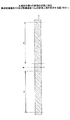
図3は、本発明の第1の実施の形態に係るビルドアップ配線層を有する集合配線基板10を例示する平面図である。図4は、本発明の第1の実施の形態に係るビルドアップ配線層を有する集合配線基板10を例示する断面図である。
本発明の第1の実施の形態の変形例では、ビルドアップ配線層を有する集合配線基板10及び配線基板10aの、本発明の第1の実施の形態とは異なる製造方法について例示する。本発明の第1の実施の形態の変形例では、支持基板11の上面に凹部13を形成せず、平坦な支持基板11の上面に第1配線層17を形成する。なお、支持基板11、剥離層15等の材料や厚さ等は、本発明の第1の実施の形態の場合と同様であるため、その説明は省略する。
本発明の第2の実施の形態では、ビルドアップ配線層を有する集合配線基板10及び配線基板10aの、本発明の第1の実施の形態とは異なる製造方法について例示する。本発明の第2の実施の形態に係る方法で製造された集合配線基板及び配線基板を、便宜上、集合配線基板30及び配線基板30aとする。集合配線基板10及び配線基板10aと集合配線基板30及び配線基板30aは製造方法が異なるが、物としては同一である。
本発明の第3の実施の形態では、ビルドアップ配線層を有する集合配線基板10及び配線基板10aの、本発明の第1の実施の形態とは異なる製造方法について例示する。本発明の第3の実施の形態に係る方法で製造された集合配線基板及び配線基板を、便宜上、集合配線基板40及び配線基板40aとする。集合配線基板10及び配線基板10aと集合配線基板40及び配線基板40aは製造方法が異なるが、物としては同一である。
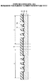
図36は、本発明の第4の実施の形態に係るビルドアップ配線層を有する集合配線基板50を例示する底面図である。図37は、本発明の第4の実施の形態に係るビルドアップ配線層を有する集合配線基板50を例示する断面図である。図36及び図37において、図3及び図4と同一部品については、同一符号を付し、その説明は省略する場合がある。図36及び図37において、59は補強枠、Cは半導体チップが実装される領域(以下、「半導体チップ実装領域C」とする)を示している。
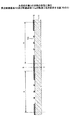
図38は、本発明の第5の実施の形態に係るビルドアップ配線層を有する集合配線基板60を例示する断面図である。なお、本発明の第5の実施の形態に係るビルドアップ配線層を有する集合配線基板60を例示する平面図は、図3と同一であるため、図示及び説明は省略する。但し、集合配線基板60において、支持基板11、第1金属層64及び剥離層65は除去しておいても構わない。
本発明の第6の実施の形態では、本発明に係る配線基板に半導体チップを実装した半導体パッケージの形態、及び、本発明に係る半導体パッケージの製造方法について例示する。
10a,60a,100 配線基板
11,41,111 支持基板
12,62,19 レジスト膜
12x,19x,27x,62x,77x,270x 開口部
13,63 凹部
14,34,64 第1金属層
15,35,65 剥離層
16,66,160 第1絶縁層
16x,66x,160x 第1ビアホール
17,67,170 第1配線層
18,68 第2金属層
20,70,200 第2配線層
21,71,210 第2絶縁層
21x,71x,210x 第2ビアホール
22,72 第3金属層
23,73,230 第3配線層
24,74,240 第3絶縁層
24x,74x,240x 第3ビアホール
25,75 第4金属層
26,76,260 第4配線層
27,77,270 ソルダーレジスト
28 補助基板
29 スタンパー
29a 凸形状
41a 貫通電極
59 補強枠
78 第5金属層
80,90,110,800 半導体パッケージ
81,810 半導体チップ
82,820 ボール状端子
83,830 アンダーフィル樹脂
290 はんだバンプ
A ビルドアップ配線層形成領域
B 切断位置
C 半導体チップ実装領域
H1 高さ
P1 第1配線層170のピッチ
P2 ボール状端子820のピッチ
P3 第1配線層17のピッチ
P4 第5金属層78のピッチ
Claims (12)
- 支持基板上に配線層及び絶縁層を積層する工程と、前記支持基板を除去する工程とを含む工程により製造される、半導体チップが実装される半導体チップ実装面を有する配線基板の製造方法であって、
前記半導体チップを構成する半導体基板と同等の熱膨張率を有する材料からなる支持基板の上面に凹部を形成する工程、前記凹部が形成された前記支持基板の上面に金属層を形成する工程、及び前記金属層上に剥離層を形成する工程を含む剥離層形成工程と、
前記剥離層上に第1絶縁層を形成する第1絶縁層形成工程と、
前記凹部に対応する位置の前記金属層が露出するように、前記剥離層及び前記第1絶縁層を貫通する貫通穴を形成する貫通穴形成工程と、
前記金属層をシード層として、前記貫通穴内に露出した前記金属層上に第1配線層を形成する第1配線層形成工程と、
前記第1配線層及び前記第1絶縁層上に更に配線層及び絶縁層を積層する積層工程と
前記剥離層に所定の処理を施すことにより、前記支持基板を除去する支持基板除去工程とを有することを特徴とする配線基板の製造方法。 - 前記貫通穴は、前記貫通穴に対応する凸形状が形成された面を有するスタンパーを用いて、前記凸形状を転写することにより形成されることを特徴とする請求項1記載の配線基板の製造方法。
- 前記第1配線層は、前記半導体チップの対応する電極と電気的に接続される電極パッドとして機能することを特徴とする請求項1又は2記載の配線基板の製造方法。
- 前記剥離層は、熱エネルギーを付与すると粘着力が低下する部材を貼り付けることにより形成され、前記所定の処理は、前記熱エネルギーを付与する処理であることを特徴とする請求項1乃至3の何れか一項記載の配線基板の製造方法。
- 前記剥離層は、光エネルギーを付与すると粘着力が低下する部材を貼り付けることにより形成され、前記所定の処理は、前記光エネルギーを付与する処理であることを特徴とする請求項1乃至3の何れか一項記載の配線基板の製造方法。
- 前記剥離層は、溶剤に溶解すると粘着力が低下する部材を貼り付けることにより形成され、前記所定の処理は、前記溶剤に溶解する処理であることを特徴とする請求項1乃至3の何れか一項記載の配線基板の製造方法。
- 前記剥離層は、SiO2から構成され、前記所定の処理は、前記SiO2をエッチングにより除去する処理であることを特徴とする請求項1乃至3の何れか一項記載の配線基板の製造方法。
- 更に、前記支持基板除去工程よりも前に、前記半導体チップ実装面の反対側の面に補助基板を配設する補助基板配設工程を有することを特徴とする請求項1乃至7の何れか一項記載の配線基板の製造方法。
- 更に、前記半導体チップ実装面の前記半導体チップが実装される領域の外縁部に補強枠を配設する補強枠配設工程を有することを特徴とする請求項1乃至8の何れか一項記載の配線基板の製造方法。
- 前記支持基板の、少なくとも前記半導体チップ実装面の前記半導体チップが実装される領域に対応する領域は、シリコンから構成されていることを特徴とする請求項1乃至9の何れか一項記載の配線基板の製造方法。
- 前記支持基板の、少なくとも前記半導体チップ実装面の前記半導体チップが実装される領域に対応する領域は、硼珪酸ガラスから構成されていることを特徴とする請求項1乃至9の何れか一項記載の配線基板の製造方法。
- 請求項1乃至11の何れか一項記載の製造方法で製造された配線基板の、前記半導体チップ実装面に前記半導体チップを実装する半導体チップ実装工程と、
前記半導体チップ実装面と前記半導体チップとの間に樹脂を充填する樹脂充填工程とを有することを特徴とする半導体パッケージの製造方法。
Priority Applications (2)
| Application Number | Priority Date | Filing Date | Title |
|---|---|---|---|
| JP2008050910A JP4981712B2 (ja) | 2008-02-29 | 2008-02-29 | 配線基板の製造方法及び半導体パッケージの製造方法 |
| US12/393,478 US7882626B2 (en) | 2008-02-29 | 2009-02-26 | Method of manufacturing wiring board having a semiconductor thereon |
Applications Claiming Priority (1)
| Application Number | Priority Date | Filing Date | Title |
|---|---|---|---|
| JP2008050910A JP4981712B2 (ja) | 2008-02-29 | 2008-02-29 | 配線基板の製造方法及び半導体パッケージの製造方法 |
Related Child Applications (2)
| Application Number | Title | Priority Date | Filing Date |
|---|---|---|---|
| JP2011241946A Division JP5225451B2 (ja) | 2011-11-04 | 2011-11-04 | 配線基板の製造方法及び半導体パッケージの製造方法 |
| JP2011241947A Division JP5372112B2 (ja) | 2011-11-04 | 2011-11-04 | 配線基板の製造方法及び半導体パッケージの製造方法 |
Publications (2)
| Publication Number | Publication Date |
|---|---|
| JP2009212140A JP2009212140A (ja) | 2009-09-17 |
| JP4981712B2 true JP4981712B2 (ja) | 2012-07-25 |
Family
ID=41052100
Family Applications (1)
| Application Number | Title | Priority Date | Filing Date |
|---|---|---|---|
| JP2008050910A Active JP4981712B2 (ja) | 2008-02-29 | 2008-02-29 | 配線基板の製造方法及び半導体パッケージの製造方法 |
Country Status (2)
| Country | Link |
|---|---|
| US (1) | US7882626B2 (ja) |
| JP (1) | JP4981712B2 (ja) |
Families Citing this family (25)
| Publication number | Priority date | Publication date | Assignee | Title |
|---|---|---|---|---|
| JP5367523B2 (ja) * | 2009-09-25 | 2013-12-11 | 新光電気工業株式会社 | 配線基板及び配線基板の製造方法 |
| TWI427716B (zh) | 2010-06-04 | 2014-02-21 | 矽品精密工業股份有限公司 | 無載具之半導體封裝件及其製法 |
| US8716873B2 (en) | 2010-07-01 | 2014-05-06 | United Test And Assembly Center Ltd. | Semiconductor packages and methods of packaging semiconductor devices |
| US20120098129A1 (en) * | 2010-10-22 | 2012-04-26 | Harris Corporation | Method of making a multi-chip module having a reduced thickness and related devices |
| US8698303B2 (en) | 2010-11-23 | 2014-04-15 | Ibiden Co., Ltd. | Substrate for mounting semiconductor, semiconductor device and method for manufacturing semiconductor device |
| JP2012169591A (ja) | 2011-01-24 | 2012-09-06 | Ngk Spark Plug Co Ltd | 多層配線基板 |
| JP5530955B2 (ja) | 2011-02-21 | 2014-06-25 | 日本特殊陶業株式会社 | 多層配線基板 |
| DE102011106104B4 (de) * | 2011-06-09 | 2014-04-10 | Otto Bock Healthcare Products Gmbh | Verfahren zum Herstellen bestückter Leiterplatten |
| US20130168132A1 (en) * | 2011-12-29 | 2013-07-04 | Sumsung Electro-Mechanics Co., Ltd. | Printed circuit board and method of manufacturing the same |
| JP5819218B2 (ja) | 2012-02-23 | 2015-11-18 | ルネサスエレクトロニクス株式会社 | 半導体装置 |
| JP5516619B2 (ja) * | 2012-02-27 | 2014-06-11 | イビデン株式会社 | 電子部品の製造方法 |
| WO2014024250A1 (ja) * | 2012-08-06 | 2014-02-13 | 古河電気工業株式会社 | 配線基板およびその製造方法ならびに半導体装置 |
| KR20140020505A (ko) * | 2012-08-09 | 2014-02-19 | 삼성전기주식회사 | 인덕터 소자 및 이의 제조 방법 |
| US9087777B2 (en) | 2013-03-14 | 2015-07-21 | United Test And Assembly Center Ltd. | Semiconductor packages and methods of packaging semiconductor devices |
| US9165878B2 (en) * | 2013-03-14 | 2015-10-20 | United Test And Assembly Center Ltd. | Semiconductor packages and methods of packaging semiconductor devices |
| JP6158676B2 (ja) * | 2013-10-15 | 2017-07-05 | 新光電気工業株式会社 | 配線基板、半導体装置及び配線基板の製造方法 |
| JP6077436B2 (ja) * | 2013-11-28 | 2017-02-08 | 京セラ株式会社 | 配線基板および配線基板への半導体素子の実装方法 |
| JP6000297B2 (ja) * | 2014-03-17 | 2016-09-28 | 聯致科技股▲フン▼有限公司 | パッケージ基板 |
| JP2015231003A (ja) * | 2014-06-06 | 2015-12-21 | イビデン株式会社 | 回路基板および回路基板の製造方法 |
| US9899239B2 (en) * | 2015-11-06 | 2018-02-20 | Apple Inc. | Carrier ultra thin substrate |
| TWI628062B (zh) * | 2016-03-17 | 2018-07-01 | 欣興電子股份有限公司 | 線路板的製作方法與感壓印模 |
| US20190292415A1 (en) * | 2016-11-28 | 2019-09-26 | Mitsui Mining & Smelting Co., Ltd. | Adhesive sheet and method for peeling same |
| TWI655741B (zh) * | 2018-01-10 | 2019-04-01 | 矽品精密工業股份有限公司 | 電子封裝件 |
| US11728278B2 (en) * | 2019-03-25 | 2023-08-15 | Taiwan Semiconductor Manufacturing Company, Ltd. | Board substrates, three-dimensional integrated circuit structures and methods of forming the same |
| US11637060B2 (en) | 2019-07-18 | 2023-04-25 | Unimicron Technology Corp. | Wiring board and method of manufacturing the same |
Family Cites Families (8)
| Publication number | Priority date | Publication date | Assignee | Title |
|---|---|---|---|---|
| JP3635219B2 (ja) | 1999-03-11 | 2005-04-06 | 新光電気工業株式会社 | 半導体装置用多層基板及びその製造方法 |
| JP3269815B2 (ja) * | 1999-12-13 | 2002-04-02 | 富士通株式会社 | 半導体装置及びその製造方法 |
| CN101024315A (zh) * | 2001-07-06 | 2007-08-29 | 钟渊化学工业株式会社 | 层压体及其制造方法 |
| JP2004039867A (ja) * | 2002-07-03 | 2004-02-05 | Sony Corp | 多層配線回路モジュール及びその製造方法 |
| JP4052955B2 (ja) * | 2003-02-06 | 2008-02-27 | Necエレクトロニクス株式会社 | 半導体装置の製造方法 |
| JP2006339365A (ja) * | 2005-06-01 | 2006-12-14 | Mitsui Mining & Smelting Co Ltd | 配線基板およびその製造方法、多層積層配線基板の製造方法並びにビアホールの形成方法 |
| CN101356641B (zh) * | 2006-01-06 | 2011-05-18 | 日本电气株式会社 | 半导体搭载用布线基板、其制造方法及布线基板组件 |
| JP2008258520A (ja) * | 2007-04-09 | 2008-10-23 | Shinko Electric Ind Co Ltd | 配線基板の製造方法及び配線基板 |
-
2008
- 2008-02-29 JP JP2008050910A patent/JP4981712B2/ja active Active
-
2009
- 2009-02-26 US US12/393,478 patent/US7882626B2/en active Active
Also Published As
| Publication number | Publication date |
|---|---|
| US20090223046A1 (en) | 2009-09-10 |
| JP2009212140A (ja) | 2009-09-17 |
| US7882626B2 (en) | 2011-02-08 |
Similar Documents
| Publication | Publication Date | Title |
|---|---|---|
| JP4981712B2 (ja) | 配線基板の製造方法及び半導体パッケージの製造方法 | |
| JP5410660B2 (ja) | 配線基板及びその製造方法と電子部品装置及びその製造方法 | |
| JP4866268B2 (ja) | 配線基板の製造方法及び電子部品装置の製造方法 | |
| JP4551321B2 (ja) | 電子部品実装構造及びその製造方法 | |
| JP5306634B2 (ja) | 配線基板及び半導体装置及び配線基板の製造方法 | |
| JP5864180B2 (ja) | 半導体パッケージ及びその製造方法 | |
| JP2010034403A (ja) | 配線基板及び電子部品装置 | |
| JP6029958B2 (ja) | 配線基板の製造方法 | |
| JP5942823B2 (ja) | 電子部品装置の製造方法、電子部品装置及び電子装置 | |
| JP2013120771A (ja) | 配線基板の製造方法、及び、配線基板製造用の支持体 | |
| JP6691451B2 (ja) | 配線基板及びその製造方法と電子部品装置 | |
| JP5007164B2 (ja) | 多層配線板及び多層配線板製造方法 | |
| JP5225451B2 (ja) | 配線基板の製造方法及び半導体パッケージの製造方法 | |
| JP5372112B2 (ja) | 配線基板の製造方法及び半導体パッケージの製造方法 | |
| JP2004119729A (ja) | 回路装置の製造方法 | |
| JP4413798B2 (ja) | 半導体装置の製造方法 | |
| JP4837696B2 (ja) | 配線基板の製造方法及び半導体装置の製造方法 | |
| JP5432354B2 (ja) | 配線基板製造用の仮基板及びその製造方法 | |
| JP2013171916A (ja) | 半導体装置の製造方法 | |
| JP3891766B2 (ja) | 多層フレキシブル配線基板の製造方法およびそれにより作製される多層フレキシブル配線基板 | |
| JP7052464B2 (ja) | 微細配線層付きコアレス基板の製造方法、および半導体パッケージの製造方法 | |
| WO2020085382A1 (ja) | 半導体パッケージ用配線基板、および半導体パッケージ用配線基板の製造方法 | |
| JP2017174953A (ja) | プリント配線板およびプリント配線板の製造方法 | |
| JP7087369B2 (ja) | 微細配線層付きキャリア基板および微細配線層付き半導体パッケージ基板の製造方法 | |
| JP5436836B2 (ja) | 半導体装置内蔵基板の製造方法 |
Legal Events
| Date | Code | Title | Description |
|---|---|---|---|
| A621 | Written request for application examination |
Free format text: JAPANESE INTERMEDIATE CODE: A621 Effective date: 20101124 |
|
| A977 | Report on retrieval |
Free format text: JAPANESE INTERMEDIATE CODE: A971007 Effective date: 20110901 |
|
| A131 | Notification of reasons for refusal |
Free format text: JAPANESE INTERMEDIATE CODE: A131 Effective date: 20110906 |
|
| A521 | Written amendment |
Free format text: JAPANESE INTERMEDIATE CODE: A523 Effective date: 20111104 |
|
| TRDD | Decision of grant or rejection written | ||
| A01 | Written decision to grant a patent or to grant a registration (utility model) |
Free format text: JAPANESE INTERMEDIATE CODE: A01 Effective date: 20120417 |
|
| A01 | Written decision to grant a patent or to grant a registration (utility model) |
Free format text: JAPANESE INTERMEDIATE CODE: A01 |
|
| A61 | First payment of annual fees (during grant procedure) |
Free format text: JAPANESE INTERMEDIATE CODE: A61 Effective date: 20120420 |
|
| FPAY | Renewal fee payment (event date is renewal date of database) |
Free format text: PAYMENT UNTIL: 20150427 Year of fee payment: 3 |
|
| R150 | Certificate of patent or registration of utility model |
Ref document number: 4981712 Country of ref document: JP Free format text: JAPANESE INTERMEDIATE CODE: R150 Free format text: JAPANESE INTERMEDIATE CODE: R150 |