JP4766049B2 - 部品内蔵モジュールの製造方法および部品内蔵モジュール - Google Patents
部品内蔵モジュールの製造方法および部品内蔵モジュール Download PDFInfo
- Publication number
- JP4766049B2 JP4766049B2 JP2007536418A JP2007536418A JP4766049B2 JP 4766049 B2 JP4766049 B2 JP 4766049B2 JP 2007536418 A JP2007536418 A JP 2007536418A JP 2007536418 A JP2007536418 A JP 2007536418A JP 4766049 B2 JP4766049 B2 JP 4766049B2
- Authority
- JP
- Japan
- Prior art keywords
- resin layer
- component
- land
- component mounting
- module
- Prior art date
- Legal status (The legal status is an assumption and is not a legal conclusion. Google has not performed a legal analysis and makes no representation as to the accuracy of the status listed.)
- Active
Links
Images


Classifications
-
- H—ELECTRICITY
- H05—ELECTRIC TECHNIQUES NOT OTHERWISE PROVIDED FOR
- H05K—PRINTED CIRCUITS; CASINGS OR CONSTRUCTIONAL DETAILS OF ELECTRIC APPARATUS; MANUFACTURE OF ASSEMBLAGES OF ELECTRICAL COMPONENTS
- H05K1/00—Printed circuits
- H05K1/18—Printed circuits structurally associated with non-printed electric components
- H05K1/182—Printed circuits structurally associated with non-printed electric components associated with components mounted in the printed circuit board, e.g. insert mounted components [IMC]
- H05K1/185—Components encapsulated in the insulating substrate of the printed circuit or incorporated in internal layers of a multilayer circuit
- H05K1/186—Components encapsulated in the insulating substrate of the printed circuit or incorporated in internal layers of a multilayer circuit manufactured by mounting on or connecting to patterned circuits before or during embedding
- H05K1/187—Components encapsulated in the insulating substrate of the printed circuit or incorporated in internal layers of a multilayer circuit manufactured by mounting on or connecting to patterned circuits before or during embedding the patterned circuits being prefabricated circuits, which are not yet attached to a permanent insulating substrate, e.g. on a temporary carrier
-
- H—ELECTRICITY
- H01—ELECTRIC ELEMENTS
- H01L—SEMICONDUCTOR DEVICES NOT COVERED BY CLASS H10
- H01L24/00—Arrangements for connecting or disconnecting semiconductor or solid-state bodies; Methods or apparatus related thereto
- H01L24/01—Means for bonding being attached to, or being formed on, the surface to be connected, e.g. chip-to-package, die-attach, "first-level" interconnects; Manufacturing methods related thereto
- H01L24/18—High density interconnect [HDI] connectors; Manufacturing methods related thereto
- H01L24/23—Structure, shape, material or disposition of the high density interconnect connectors after the connecting process
- H01L24/24—Structure, shape, material or disposition of the high density interconnect connectors after the connecting process of an individual high density interconnect connector
-
- H—ELECTRICITY
- H01—ELECTRIC ELEMENTS
- H01L—SEMICONDUCTOR DEVICES NOT COVERED BY CLASS H10
- H01L24/00—Arrangements for connecting or disconnecting semiconductor or solid-state bodies; Methods or apparatus related thereto
- H01L24/80—Methods for connecting semiconductor or other solid state bodies using means for bonding being attached to, or being formed on, the surface to be connected
- H01L24/82—Methods for connecting semiconductor or other solid state bodies using means for bonding being attached to, or being formed on, the surface to be connected by forming build-up interconnects at chip-level, e.g. for high density interconnects [HDI]
-
- H—ELECTRICITY
- H01—ELECTRIC ELEMENTS
- H01L—SEMICONDUCTOR DEVICES NOT COVERED BY CLASS H10
- H01L24/00—Arrangements for connecting or disconnecting semiconductor or solid-state bodies; Methods or apparatus related thereto
- H01L24/93—Batch processes
- H01L24/95—Batch processes at chip-level, i.e. with connecting carried out on a plurality of singulated devices, i.e. on diced chips
- H01L24/96—Batch processes at chip-level, i.e. with connecting carried out on a plurality of singulated devices, i.e. on diced chips the devices being encapsulated in a common layer, e.g. neo-wafer or pseudo-wafer, said common layer being separable into individual assemblies after connecting
-
- H—ELECTRICITY
- H05—ELECTRIC TECHNIQUES NOT OTHERWISE PROVIDED FOR
- H05K—PRINTED CIRCUITS; CASINGS OR CONSTRUCTIONAL DETAILS OF ELECTRIC APPARATUS; MANUFACTURE OF ASSEMBLAGES OF ELECTRICAL COMPONENTS
- H05K3/00—Apparatus or processes for manufacturing printed circuits
- H05K3/46—Manufacturing multilayer circuits
-
- H—ELECTRICITY
- H01—ELECTRIC ELEMENTS
- H01L—SEMICONDUCTOR DEVICES NOT COVERED BY CLASS H10
- H01L21/00—Processes or apparatus adapted for the manufacture or treatment of semiconductor or solid state devices or of parts thereof
- H01L21/02—Manufacture or treatment of semiconductor devices or of parts thereof
- H01L21/04—Manufacture or treatment of semiconductor devices or of parts thereof the devices having at least one potential-jump barrier or surface barrier, e.g. PN junction, depletion layer or carrier concentration layer
- H01L21/50—Assembly of semiconductor devices using processes or apparatus not provided for in a single one of the subgroups H01L21/06 - H01L21/326, e.g. sealing of a cap to a base of a container
- H01L21/56—Encapsulations, e.g. encapsulation layers, coatings
- H01L21/568—Temporary substrate used as encapsulation process aid
-
- H—ELECTRICITY
- H01—ELECTRIC ELEMENTS
- H01L—SEMICONDUCTOR DEVICES NOT COVERED BY CLASS H10
- H01L2224/00—Indexing scheme for arrangements for connecting or disconnecting semiconductor or solid-state bodies and methods related thereto as covered by H01L24/00
- H01L2224/01—Means for bonding being attached to, or being formed on, the surface to be connected, e.g. chip-to-package, die-attach, "first-level" interconnects; Manufacturing methods related thereto
- H01L2224/02—Bonding areas; Manufacturing methods related thereto
- H01L2224/04—Structure, shape, material or disposition of the bonding areas prior to the connecting process
- H01L2224/04105—Bonding areas formed on an encapsulation of the semiconductor or solid-state body, e.g. bonding areas on chip-scale packages
-
- H—ELECTRICITY
- H01—ELECTRIC ELEMENTS
- H01L—SEMICONDUCTOR DEVICES NOT COVERED BY CLASS H10
- H01L2224/00—Indexing scheme for arrangements for connecting or disconnecting semiconductor or solid-state bodies and methods related thereto as covered by H01L24/00
- H01L2224/01—Means for bonding being attached to, or being formed on, the surface to be connected, e.g. chip-to-package, die-attach, "first-level" interconnects; Manufacturing methods related thereto
- H01L2224/10—Bump connectors; Manufacturing methods related thereto
- H01L2224/15—Structure, shape, material or disposition of the bump connectors after the connecting process
- H01L2224/16—Structure, shape, material or disposition of the bump connectors after the connecting process of an individual bump connector
- H01L2224/161—Disposition
- H01L2224/16151—Disposition the bump connector connecting between a semiconductor or solid-state body and an item not being a semiconductor or solid-state body, e.g. chip-to-substrate, chip-to-passive
- H01L2224/16221—Disposition the bump connector connecting between a semiconductor or solid-state body and an item not being a semiconductor or solid-state body, e.g. chip-to-substrate, chip-to-passive the body and the item being stacked
- H01L2224/16225—Disposition the bump connector connecting between a semiconductor or solid-state body and an item not being a semiconductor or solid-state body, e.g. chip-to-substrate, chip-to-passive the body and the item being stacked the item being non-metallic, e.g. insulating substrate with or without metallisation
- H01L2224/16238—Disposition the bump connector connecting between a semiconductor or solid-state body and an item not being a semiconductor or solid-state body, e.g. chip-to-substrate, chip-to-passive the body and the item being stacked the item being non-metallic, e.g. insulating substrate with or without metallisation the bump connector connecting to a bonding area protruding from the surface of the item
-
- H—ELECTRICITY
- H01—ELECTRIC ELEMENTS
- H01L—SEMICONDUCTOR DEVICES NOT COVERED BY CLASS H10
- H01L2224/00—Indexing scheme for arrangements for connecting or disconnecting semiconductor or solid-state bodies and methods related thereto as covered by H01L24/00
- H01L2224/01—Means for bonding being attached to, or being formed on, the surface to be connected, e.g. chip-to-package, die-attach, "first-level" interconnects; Manufacturing methods related thereto
- H01L2224/18—High density interconnect [HDI] connectors; Manufacturing methods related thereto
- H01L2224/23—Structure, shape, material or disposition of the high density interconnect connectors after the connecting process
- H01L2224/24—Structure, shape, material or disposition of the high density interconnect connectors after the connecting process of an individual high density interconnect connector
- H01L2224/241—Disposition
- H01L2224/24151—Connecting between a semiconductor or solid-state body and an item not being a semiconductor or solid-state body, e.g. chip-to-substrate, chip-to-passive
- H01L2224/24153—Connecting between a semiconductor or solid-state body and an item not being a semiconductor or solid-state body, e.g. chip-to-substrate, chip-to-passive the body and the item being arranged next to each other, e.g. on a common substrate
- H01L2224/24195—Connecting between a semiconductor or solid-state body and an item not being a semiconductor or solid-state body, e.g. chip-to-substrate, chip-to-passive the body and the item being arranged next to each other, e.g. on a common substrate the item being a discrete passive component
-
- H—ELECTRICITY
- H01—ELECTRIC ELEMENTS
- H01L—SEMICONDUCTOR DEVICES NOT COVERED BY CLASS H10
- H01L2924/00—Indexing scheme for arrangements or methods for connecting or disconnecting semiconductor or solid-state bodies as covered by H01L24/00
- H01L2924/15—Details of package parts other than the semiconductor or other solid state devices to be connected
- H01L2924/151—Die mounting substrate
- H01L2924/1517—Multilayer substrate
- H01L2924/15192—Resurf arrangement of the internal vias
-
- H—ELECTRICITY
- H01—ELECTRIC ELEMENTS
- H01L—SEMICONDUCTOR DEVICES NOT COVERED BY CLASS H10
- H01L2924/00—Indexing scheme for arrangements or methods for connecting or disconnecting semiconductor or solid-state bodies as covered by H01L24/00
- H01L2924/15—Details of package parts other than the semiconductor or other solid state devices to be connected
- H01L2924/181—Encapsulation
-
- H—ELECTRICITY
- H01—ELECTRIC ELEMENTS
- H01L—SEMICONDUCTOR DEVICES NOT COVERED BY CLASS H10
- H01L2924/00—Indexing scheme for arrangements or methods for connecting or disconnecting semiconductor or solid-state bodies as covered by H01L24/00
- H01L2924/19—Details of hybrid assemblies other than the semiconductor or other solid state devices to be connected
- H01L2924/191—Disposition
- H01L2924/19101—Disposition of discrete passive components
- H01L2924/19105—Disposition of discrete passive components in a side-by-side arrangement on a common die mounting substrate
-
- H—ELECTRICITY
- H01—ELECTRIC ELEMENTS
- H01L—SEMICONDUCTOR DEVICES NOT COVERED BY CLASS H10
- H01L2924/00—Indexing scheme for arrangements or methods for connecting or disconnecting semiconductor or solid-state bodies as covered by H01L24/00
- H01L2924/30—Technical effects
- H01L2924/301—Electrical effects
- H01L2924/3025—Electromagnetic shielding
-
- H—ELECTRICITY
- H05—ELECTRIC TECHNIQUES NOT OTHERWISE PROVIDED FOR
- H05K—PRINTED CIRCUITS; CASINGS OR CONSTRUCTIONAL DETAILS OF ELECTRIC APPARATUS; MANUFACTURE OF ASSEMBLAGES OF ELECTRICAL COMPONENTS
- H05K2201/00—Indexing scheme relating to printed circuits covered by H05K1/00
- H05K2201/07—Electric details
- H05K2201/0707—Shielding
- H05K2201/0715—Shielding provided by an outer layer of PCB
-
- H—ELECTRICITY
- H05—ELECTRIC TECHNIQUES NOT OTHERWISE PROVIDED FOR
- H05K—PRINTED CIRCUITS; CASINGS OR CONSTRUCTIONAL DETAILS OF ELECTRIC APPARATUS; MANUFACTURE OF ASSEMBLAGES OF ELECTRICAL COMPONENTS
- H05K2201/00—Indexing scheme relating to printed circuits covered by H05K1/00
- H05K2201/09—Shape and layout
- H05K2201/09209—Shape and layout details of conductors
- H05K2201/095—Conductive through-holes or vias
- H05K2201/096—Vertically aligned vias, holes or stacked vias
-
- H—ELECTRICITY
- H05—ELECTRIC TECHNIQUES NOT OTHERWISE PROVIDED FOR
- H05K—PRINTED CIRCUITS; CASINGS OR CONSTRUCTIONAL DETAILS OF ELECTRIC APPARATUS; MANUFACTURE OF ASSEMBLAGES OF ELECTRICAL COMPONENTS
- H05K3/00—Apparatus or processes for manufacturing printed circuits
- H05K3/10—Apparatus or processes for manufacturing printed circuits in which conductive material is applied to the insulating support in such a manner as to form the desired conductive pattern
- H05K3/20—Apparatus or processes for manufacturing printed circuits in which conductive material is applied to the insulating support in such a manner as to form the desired conductive pattern by affixing prefabricated conductor pattern
-
- H—ELECTRICITY
- H05—ELECTRIC TECHNIQUES NOT OTHERWISE PROVIDED FOR
- H05K—PRINTED CIRCUITS; CASINGS OR CONSTRUCTIONAL DETAILS OF ELECTRIC APPARATUS; MANUFACTURE OF ASSEMBLAGES OF ELECTRICAL COMPONENTS
- H05K3/00—Apparatus or processes for manufacturing printed circuits
- H05K3/46—Manufacturing multilayer circuits
- H05K3/4644—Manufacturing multilayer circuits by building the multilayer layer by layer, i.e. build-up multilayer circuits
Description
特許文献1の図2には、パターンニングされていないベタの銅箔上に回路部品を実装し、回路部品を樹脂で固めた後で、裏側から銅箔をエッチングすることにより回路パターンを形成する方法が記載されている。
また、特許文献1の図3には、離型フィルム上に回路パターンを形成し、その上に回路部品を実装し、回路部品を樹脂で固めた後、離型フィルムを剥がす方法が記載されている。
同様に、ICのように半田バンプを用いて実装する場合に、リフロー時に溶融したバンプが配線部分に流れて形状が変形することがないので、実装信頼性の劣化を防ぐことができる。
上記のように部品の動きに伴う部品同士の接触や、端子間の短絡を考慮する必要がなくなるので、より高密度に部品実装することが可能になり、モジュールの小型化、高機能化を図ることができる。
さらに、部品実装面にはんだレジスト膜を形成する必要がないので、モジュールの薄型・低背化を損なうことがなく、工程の削減、コスト低減を実現できるとともに、部品実装面と樹脂層とが強く密着するので、半田フラッシュの発生を抑えることができる。また、配線とレジストの位置ずれを見込む必要がないので、ランド間距離を短くでき、狭端子ピッチの部品や、チップ部品間を狭隣接に実装することができる。
回路部品をランドに半田付けする場合、溶融した半田のために回路部品が動きやすいが、ランドが島状に形成されている(配線部分と連続していない)ため、回路部品の動きがランドの範囲内に制約され、動きを抑制できるとともに、半田の流れを規制でき、異なる電位部分との短絡を防止できる。
基板となる樹脂層の裏面に配線パターンを形成した場合、樹脂層の表面にも導体パターンを形成し、この導体パターンと配線パターンとをビアホールを介して接続する必要が生じることがある。その場合に、部品実装用ランドと同時にビアランドを形成しておけば、ビアホールとビアランドとの導通が確実になり、信頼性の高い部品内蔵モジュールを実現できる。
回路部品をランドに半田付けすると、半田がランドの側面に回り込み、樹脂層の裏面に露出することがある。このような状態で、第5の工程においてめっき工法にて配線パターンを形成する場合、エッチング処理の際に露出した半田がエッチング液により侵食され、半田接合の信頼性が低下する時がある。この不具合を回避するために、配線パターンは部品実装用ランドを覆い、かつ部品実装ランドの外周より幾分大きくなるように形成する。これにより、樹脂層裏面に露出した半田を配線パターンが覆うため、エッチング液による半田の侵食を防止できる。配線パターンは樹脂層の裏面に露出した半田を十分に覆う形状にすることがさらに望ましい。
上述したように配線パターンを形成することにより、更に以下のような効果を奏する。配線パターン自体が半田を覆うことにより、ソルダーレジストを使用することなく半田の露出を防止できる。このため回路基板への実装時の熱膨張でソルダーレジストと樹脂層との界面に空隙が発生するという問題が生じず、この空隙への半田の流れ出しを防止できる。
本部品内蔵モジュールを回路基板(マザーボード)などに実装する場合、配線パターンが形成された樹脂層の裏面を実装面としてもよいが、配線パターンが露出しているため、配線パターンが回路基板の異電位部分と短絡する恐れがある。その場合、配線パターンをレジスト膜のような絶縁膜で覆ってもよいが、実装面と配線パターンとが近いため、回路基板への実装時の高温でランドに接続された回路部品の半田が再溶融しやすくなる。そこで、樹脂層の裏面に更なる樹脂層を積層し、その樹脂層の裏面に端子電極を形成することで、配線パターンを他の部分と絶縁できるとともに、樹脂層の断熱効果によって回路基板への実装時の熱による影響を小さくでき、回路部品の半田の再溶融を抑制できる。
配線パターンが形成された樹脂層の裏面に積層されるさらなる樹脂層は、1層でもよいし、2層以上であってもよい。この更なる樹脂層の中に、別の回路部品を内蔵してもよいし、配線パターンを形成してもよい。望ましくは、最下層の樹脂層には回路部品を内蔵しない方がよい。配線パターンと最下層の樹脂層の裏面に形成された端子電極との間とを電気的に接続するために、適宜ビアホールを用いることができる。
基板となる樹脂層の一主面に配線パターンを形成した場合、樹脂層の他主面にも導体パターンを形成し、この導体パターンと配線パターンとをビアホールを介して接続する必要が生じることがある。その場合に、部品実装用ランドと同時にビアランドを形成しておけば、ビアホールとビアランドとの導通が確実になり、信頼性の高い部品内蔵モジュールを実現できる。
また、はんだレジストを形成する必要がないので、モジュールの薄型・低背化を損なうことがなく、工程の削減、コスト低減を実現できるとともに、半田フラッシュの発生を抑えることができる。
本部品内蔵モジュールでは、部品実装用ランドが隣接する配線パターンに比べて厚肉に形成されているため、部品実装用ランドの強度が配線パターンに比べて高く、回路部品とランドとの接合強度を高めることができる。そのため、接続信頼性の高いモジュールを実現できる。
1,1A モジュール基板
2 配線パターン
3 部品実装用ランド
4,4a,4b 回路部品
5 半田
6 半田バンプ
7 ビアランド
8 ビアホール
9 導体パターン
10 端子電極
11 グランド電極
(第1の実施形態)
図1,図2は本発明にかかる部品内蔵モジュールの好ましい第1実施形態を示す。
このモジュールAは、熱硬化性樹脂よりなる電気絶縁性のモジュール基板1を備えており、モジュール基板1は上側の樹脂層1aと下側の樹脂層1bとの2層構造となっている。
モジュール基板1の内部、つまり上側の樹脂層1aと下側の樹脂層1bとの境界面には、複数の部品実装用ランド3とそれらを接続する配線パターン2が設けられている。ランド3は、図2(a)に示すように配線パターン2の上に重ねて形成されており、ランド部分は2層構造となっている。ランド3は上側の樹脂層1aに埋設されており、配線パターン2は下側の樹脂層1bに埋設されている。
導体パターン9およびグランド電極11は、レジスト膜13、14によって覆われている。なお、導体パターン9を覆うレジスト膜13を全面的あるいは部分的に除去し、導体パターン9に別の回路部品を実装してもよいことは勿論である。
下側の樹脂層1bは回路基板(マザーボード)への実装面を構成する樹脂層であり、本モジュールAを回路基板に実装する際に高温に晒される可能性があるため、樹脂層1bの内部には回路部品4を内蔵しない方が望ましい。
まず、図3の(a)に示すように、転写板20の上に複数の部品実装用ランド3とビアランド7とを島状に独立して形成する。つまり、各ランド3,7は互いに配線部分を介して接続されていない。転写板20とは、金属板や樹脂板のような硬質板であってもよいが、離型フィルムを用いてもよい。部品実装用ランド3とビアランド7の形成方法としては、例えば転写板20の上に銅箔を貼り、エッチングによりランド3,7をパターン形成すればよい。その他に、公知の厚膜形成法あるいは薄膜形成法により転写板20の上にパターン化されたランド3,7を直接形成してもよい。
なお、ビアホール8については、予め樹脂層1aに設けておく代わりに、樹脂層1aの加熱硬化後にレーザーで穴をあけ、導体パターン9と同時にめっきで形成してもよい。
なお、図3,図4では、単一のモジュールAの製造方法について説明したが、実際には平面方向に連続するマザー状態の樹脂層1a,1bを用いてマザー状態のモジュールを製作し、その後で個別のモジュールにカットすることで、量産性が高く均質な製造方法を実現できる。
図6は、図3(f)のVI部分を樹脂層1aの下側から見た図であり、図7は図4(h)のVII部分を樹脂層1aの下側から見た図である。図7に示すように、配線パターン2は、それぞれ対応するランド3を覆い、かつランド3の外周より大きく形成することが好ましい。ランド3上に回路部品4(4a,4b)を実装する際に半田6を塗布すると、図6のように半田6がランド3上に納まらず、樹脂層1aの下面に露出する場合がある。このとき図7のように配線パターンを形成すると、半田6が配線パターン2に覆われる。このため、樹脂層1bの下面に、めっき工法により端子電極10およびグランド電極11を形成するときに行われるエッチング処理時のエッチング液に半田6が曝されることがないため、半田侵食を防止できる。
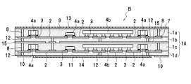
図5は本発明にかかる部品内蔵モジュールの好ましい第2実施形態を示す。なお、図1と共通する部分には同一符号を付して重複説明を省略する。
この部品内蔵モジュールBのモジュール基板1Aは、上下4層の樹脂層1a〜1dを積層したものであり、最上層1aと第2層1b、および第3層1cと最下層1dがそれぞれ第1実施形態のモジュール基板1と同様な構造を有している。すなわち、最上層1aと第2層1bの境界面には部品実装用ランド3とビアランド7とが独立して形成されるとともに、これらランド3,7を相互に接続する配線パターン2が形成されている。また、第3層1cと最下層1dとの境界面にも部品実装用ランド3とビアランド7とが独立して形成されるとともに、これらランド3,7を相互に接続する配線パターン2が形成されている。
また、回路部品4の中で、半導体素子4bのような能動素子をバンプ6を用いてフリップチップ実装したが、これに限るものではなく、端子をランド3に半田付けしてもよい。
第1の実施形態では2層構造、第2の実施形態では4層構造のモジュール基板を有する部品内蔵モジュールについて説明したが、それ以外の層構造を持つ部品内蔵モジュールであってもよいことは勿論である。その場合、各層間に導体パターンを形成して容量を形成したり、抵抗などを印刷形成するなど、公知の多層基板技術を適用してもよい。
第2実施形態では、中間層である第2層1bに回路部品4を内蔵しない例を示したが、第2層1bに回路部品4を内蔵してもよいことは勿論である。
Claims (8)
- 転写板の上に配線部を有しない複数の部品実装用ランドを島状に独立して形成する第1の工程と、
上記転写板上に形成された部品実装用ランドに回路部品を接続する第2の工程と、
上記転写板の上に上記回路部品を覆うように絶縁性の樹脂層を形成してこの樹脂層を硬化させ、上記樹脂層の内部に回路部品を埋設する第3の工程と、
上記樹脂層から上記転写板を剥離し、上記樹脂層に上記部品実装用ランドを転写する第4の工程と、
上記部品実装用ランドが露出した上記樹脂層の裏面に、上記部品実装用ランド間を接続しあるいは部品実装用ランドと他部とを接続するための配線部を上記部品実装用ランドに重ねて形成する第5の工程と、
を含む部品内蔵モジュールの製造方法。 - 上記部品実装用ランドは、上記回路部品を半田付けにより接続するためのランドであることを特徴とする請求項1に記載の部品内蔵モジュールの製造方法。
- 上記第1の工程は、上記転写板の上に上記部品実装用ランドと同時に、上記部品実装用ランドと離れたビアランドを形成する工程を含み、
上記第3の工程の後に、上記樹脂層の表面に、上記ビアランドとビアホールを介して導通する導体パターンを形成する工程を有することを特徴とする請求項1または2に記載の部品内蔵モジュールの製造方法。 - 上記第5の工程において、上記配線部は上記部品実装用ランドを覆い、かつ上記部品実装ランドの外周より大きく形成されることを特徴とする請求項1ないし3のいずれか1項に記載の部品内蔵モジュールの製造方法。
- 上記第5の工程の後、
上記配線部が形成された樹脂層の裏面に、少なくとも1層のさらなる樹脂層を積層する工程と、
上記積層された最下層の樹脂層の裏面に、上記回路部品と電気的に接続された端子電極を形成する工程と、を有することを特徴とする請求項1ないし4のいずれか1項に記載の部品内蔵モジュールの製造方法。 - 第1主面と第2主面とを有する絶縁性の樹脂層を備え、
上記樹脂層の第1主面に沿って、島状に独立した複数の部品実装用ランドとこれらランドに接続された配線部とが形成され、
上記部品実装用ランドの表面に回路部品が接続され、
上記回路部品は上記樹脂層の内部に埋設されており、
上記部品実装用ランドは、その裏面が上記樹脂層の第1主面と同一面となるように上記樹脂層に埋設されており、
上記配線部は、上記部品実装用ランドと重なるように上記樹脂層の第1主面上に形成されていることを特徴とする部品内蔵モジュール。 - 上記樹脂層の第1主面の上記部品実装用ランドと離れた位置に、上記配線部に接続されたビアランドが形成されており、
上記樹脂層の上記第1主面と対向する第2主面に、導体パターンが形成されており、
上記樹脂層には、上記ビアランドと導体パターンとを導通させるビアホールが形成されていることを特徴とする請求項6に記載の部品内蔵モジュール。 - 上記樹脂層の第1主面に、少なくとも1層のさらなる樹脂層が積層されており、
上記積層された最下層の樹脂層の裏面に、上記回路部品と電気的に接続された端子電極が形成されていることを特徴とする請求項6又は7に記載の部品内蔵モジュール。
Priority Applications (1)
| Application Number | Priority Date | Filing Date | Title |
|---|---|---|---|
| JP2007536418A JP4766049B2 (ja) | 2005-09-20 | 2006-08-03 | 部品内蔵モジュールの製造方法および部品内蔵モジュール |
Applications Claiming Priority (4)
| Application Number | Priority Date | Filing Date | Title |
|---|---|---|---|
| JP2005271275 | 2005-09-20 | ||
| JP2005271275 | 2005-09-20 | ||
| JP2007536418A JP4766049B2 (ja) | 2005-09-20 | 2006-08-03 | 部品内蔵モジュールの製造方法および部品内蔵モジュール |
| PCT/JP2006/315389 WO2007034629A1 (ja) | 2005-09-20 | 2006-08-03 | 部品内蔵モジュールの製造方法および部品内蔵モジュール |
Publications (2)
| Publication Number | Publication Date |
|---|---|
| JPWO2007034629A1 JPWO2007034629A1 (ja) | 2009-03-19 |
| JP4766049B2 true JP4766049B2 (ja) | 2011-09-07 |
Family
ID=37888684
Family Applications (1)
| Application Number | Title | Priority Date | Filing Date |
|---|---|---|---|
| JP2007536418A Active JP4766049B2 (ja) | 2005-09-20 | 2006-08-03 | 部品内蔵モジュールの製造方法および部品内蔵モジュール |
Country Status (5)
| Country | Link |
|---|---|
| US (1) | US7885081B2 (ja) |
| JP (1) | JP4766049B2 (ja) |
| KR (1) | KR100935139B1 (ja) |
| CN (1) | CN101263752B (ja) |
| WO (1) | WO2007034629A1 (ja) |
Families Citing this family (39)
| Publication number | Priority date | Publication date | Assignee | Title |
|---|---|---|---|---|
| JP4185499B2 (ja) * | 2005-02-18 | 2008-11-26 | 富士通マイクロエレクトロニクス株式会社 | 半導体装置 |
| WO2008136251A1 (ja) | 2007-05-02 | 2008-11-13 | Murata Manufacturing Co., Ltd. | 部品内蔵モジュール及びその製造方法 |
| US7838420B2 (en) * | 2007-08-29 | 2010-11-23 | Freescale Semiconductor, Inc. | Method for forming a packaged semiconductor device |
| JP5172275B2 (ja) * | 2007-10-26 | 2013-03-27 | パナソニック株式会社 | 部品内蔵プリント配線基板および部品内蔵プリント配線基板の製造方法 |
| WO2009057654A1 (ja) | 2007-11-01 | 2009-05-07 | Dai Nippon Printing Co., Ltd. | 部品内蔵配線板、部品内蔵配線板の製造方法 |
| CN102625579B (zh) * | 2008-03-27 | 2014-10-29 | 揖斐电株式会社 | 电子部件内置线路板 |
| CN102132639A (zh) * | 2008-11-06 | 2011-07-20 | 揖斐电株式会社 | 电子部件内置线路板及其制造方法 |
| WO2010073800A1 (ja) * | 2008-12-22 | 2010-07-01 | 富士通株式会社 | 電子部品とその製造方法 |
| US7851894B1 (en) * | 2008-12-23 | 2010-12-14 | Amkor Technology, Inc. | System and method for shielding of package on package (PoP) assemblies |
| JP5287220B2 (ja) * | 2008-12-24 | 2013-09-11 | 株式会社村田製作所 | 部品内蔵基板の製造方法 |
| JP5354224B2 (ja) * | 2009-11-19 | 2013-11-27 | 株式会社村田製作所 | 部品内蔵モジュールの製造方法 |
| US8304286B2 (en) * | 2009-12-11 | 2012-11-06 | Stats Chippac Ltd. | Integrated circuit packaging system with shielded package and method of manufacture thereof |
| KR101104210B1 (ko) * | 2010-03-05 | 2012-01-10 | 삼성전기주식회사 | 전자소자 내장형 인쇄회로기판 및 그 제조방법 |
| CN102237885A (zh) * | 2010-04-20 | 2011-11-09 | 国民技术股份有限公司 | 一种无线通信模块 |
| JP2011228528A (ja) * | 2010-04-21 | 2011-11-10 | Mitsubishi Electric Corp | パワーブロック及びそれを用いたパワー半導体モジュール |
| KR101085733B1 (ko) | 2010-05-28 | 2011-11-21 | 삼성전기주식회사 | 전자소자 내장 인쇄회로기판 및 그 제조방법 |
| KR101147343B1 (ko) * | 2010-05-28 | 2012-05-22 | 엘지이노텍 주식회사 | 복수의 소자가 내장된 집적 인쇄회로기판 및 그 제조 방법 |
| KR101118817B1 (ko) | 2010-07-05 | 2012-03-12 | 삼성전기주식회사 | 다층 임베디드 인쇄회로기판 및 이의 제조 방법 |
| JP5644286B2 (ja) * | 2010-09-07 | 2014-12-24 | オムロン株式会社 | 電子部品の表面実装方法及び電子部品が実装された基板 |
| KR20120026855A (ko) | 2010-09-10 | 2012-03-20 | 삼성전기주식회사 | 임베디드 볼 그리드 어레이 기판 및 그 제조 방법 |
| JP2012151353A (ja) * | 2011-01-20 | 2012-08-09 | Sharp Corp | 半導体モジュール |
| US8674235B2 (en) * | 2011-06-06 | 2014-03-18 | Intel Corporation | Microelectronic substrate for alternate package functionality |
| KR101175901B1 (ko) | 2011-10-25 | 2012-08-23 | 삼성전기주식회사 | 다층 임베디드 인쇄회로기판 및 이의 제조 방법 |
| KR101420526B1 (ko) * | 2012-11-29 | 2014-07-17 | 삼성전기주식회사 | 전자부품 내장기판 및 그 제조방법 |
| CN103035861B (zh) * | 2012-11-30 | 2014-05-21 | 苏州安洁科技股份有限公司 | 一种电池组装定位板 |
| JP2013110441A (ja) * | 2013-03-11 | 2013-06-06 | Dainippon Printing Co Ltd | 部品内蔵配線板の製造方法 |
| JP6103054B2 (ja) * | 2013-06-18 | 2017-03-29 | 株式会社村田製作所 | 樹脂多層基板の製造方法 |
| CN103607841B (zh) * | 2013-12-04 | 2016-06-01 | 江苏长电科技股份有限公司 | Smt减法高密度封装多层线路板结构及其制作方法 |
| US9859250B2 (en) * | 2013-12-20 | 2018-01-02 | Cyntec Co., Ltd. | Substrate and the method to fabricate thereof |
| KR102231100B1 (ko) * | 2014-10-02 | 2021-03-23 | 삼성전기주식회사 | 인쇄회로기판 및 그 제조 방법 |
| US10097030B2 (en) | 2016-04-29 | 2018-10-09 | Taiwan Semiconductor Manufacturing Co., Ltd | Packaged semiconductor devices with wireless charging means |
| US10269732B2 (en) * | 2016-07-20 | 2019-04-23 | Taiwan Semiconductor Manufacturing Company, Ltd. | Info package with integrated antennas or inductors |
| US10332841B2 (en) | 2016-07-20 | 2019-06-25 | Taiwan Semiconductor Manufacturing Company, Ltd. | System on integrated chips and methods of forming the same |
| US20180374798A1 (en) * | 2017-06-24 | 2018-12-27 | Amkor Technology, Inc. | Semiconductor device having emi shielding structure and related methods |
| KR101963293B1 (ko) * | 2017-11-01 | 2019-03-28 | 삼성전기주식회사 | 팬-아웃 반도체 패키지 |
| CN108513446B (zh) * | 2018-03-23 | 2019-04-23 | 北京梦之墨科技有限公司 | 一种转印模板及转印方法 |
| TWI723414B (zh) * | 2019-06-05 | 2021-04-01 | 矽品精密工業股份有限公司 | 電子封裝件及其製法 |
| US11094635B2 (en) * | 2019-08-22 | 2021-08-17 | Taiwan Semiconductor Manufacturing Co., Ltd. | Package structure and method for forming the same |
| JP6930617B2 (ja) * | 2020-02-10 | 2021-09-01 | ダイキン工業株式会社 | 電装品、および電装品の製造方法 |
Citations (6)
| Publication number | Priority date | Publication date | Assignee | Title |
|---|---|---|---|---|
| JP2002076637A (ja) * | 2000-08-29 | 2002-03-15 | Matsushita Electric Ind Co Ltd | チップ部品内蔵基板及びその製造方法 |
| JP2002223076A (ja) * | 2001-01-26 | 2002-08-09 | Ngk Spark Plug Co Ltd | 多層配線基板 |
| JP2004274035A (ja) * | 2003-02-18 | 2004-09-30 | Matsushita Electric Ind Co Ltd | 電子部品内蔵モジュールとその製造方法 |
| JP2005039158A (ja) * | 2003-07-18 | 2005-02-10 | Matsushita Electric Ind Co Ltd | 部品内蔵モジュール及びその製造方法 |
| JP2005101580A (ja) * | 2003-08-28 | 2005-04-14 | Matsushita Electric Ind Co Ltd | 回路部品内蔵モジュール及びその製造方法 |
| JP2006303202A (ja) * | 2005-04-21 | 2006-11-02 | Cmk Corp | 部品内蔵型プリント配線板とその製造方法 |
Family Cites Families (9)
| Publication number | Priority date | Publication date | Assignee | Title |
|---|---|---|---|---|
| US5027253A (en) * | 1990-04-09 | 1991-06-25 | Ibm Corporation | Printed circuit boards and cards having buried thin film capacitors and processing techniques for fabricating said boards and cards |
| JP3726985B2 (ja) * | 1996-12-09 | 2005-12-14 | ソニー株式会社 | 電子部品の製造方法 |
| US6038133A (en) | 1997-11-25 | 2000-03-14 | Matsushita Electric Industrial Co., Ltd. | Circuit component built-in module and method for producing the same |
| TW511415B (en) * | 2001-01-19 | 2002-11-21 | Matsushita Electric Ind Co Ltd | Component built-in module and its manufacturing method |
| JP2003087538A (ja) * | 2001-09-14 | 2003-03-20 | Canon Inc | 通信装置 |
| JP3910045B2 (ja) | 2001-11-05 | 2007-04-25 | シャープ株式会社 | 電子部品内装配線板の製造方法 |
| JP3789410B2 (ja) * | 2002-08-29 | 2006-06-21 | 富士通メディアデバイス株式会社 | 表面実装型電子部品モジュールおよびその製造方法 |
| US7394663B2 (en) | 2003-02-18 | 2008-07-01 | Matsushita Electric Industrial Co., Ltd. | Electronic component built-in module and method of manufacturing the same |
| US7180169B2 (en) | 2003-08-28 | 2007-02-20 | Matsushita Electric Industrial Co., Ltd. | Circuit component built-in module and method for manufacturing the same |
-
2006
- 2006-08-03 WO PCT/JP2006/315389 patent/WO2007034629A1/ja active Application Filing
- 2006-08-03 JP JP2007536418A patent/JP4766049B2/ja active Active
- 2006-08-03 CN CN2006800330433A patent/CN101263752B/zh active Active
- 2006-08-03 KR KR1020087004669A patent/KR100935139B1/ko active IP Right Grant
-
2008
- 2008-03-04 US US12/041,730 patent/US7885081B2/en active Active
Patent Citations (6)
| Publication number | Priority date | Publication date | Assignee | Title |
|---|---|---|---|---|
| JP2002076637A (ja) * | 2000-08-29 | 2002-03-15 | Matsushita Electric Ind Co Ltd | チップ部品内蔵基板及びその製造方法 |
| JP2002223076A (ja) * | 2001-01-26 | 2002-08-09 | Ngk Spark Plug Co Ltd | 多層配線基板 |
| JP2004274035A (ja) * | 2003-02-18 | 2004-09-30 | Matsushita Electric Ind Co Ltd | 電子部品内蔵モジュールとその製造方法 |
| JP2005039158A (ja) * | 2003-07-18 | 2005-02-10 | Matsushita Electric Ind Co Ltd | 部品内蔵モジュール及びその製造方法 |
| JP2005101580A (ja) * | 2003-08-28 | 2005-04-14 | Matsushita Electric Ind Co Ltd | 回路部品内蔵モジュール及びその製造方法 |
| JP2006303202A (ja) * | 2005-04-21 | 2006-11-02 | Cmk Corp | 部品内蔵型プリント配線板とその製造方法 |
Also Published As
| Publication number | Publication date |
|---|---|
| KR100935139B1 (ko) | 2010-01-06 |
| US20080149381A1 (en) | 2008-06-26 |
| JPWO2007034629A1 (ja) | 2009-03-19 |
| CN101263752B (zh) | 2010-06-09 |
| CN101263752A (zh) | 2008-09-10 |
| WO2007034629A1 (ja) | 2007-03-29 |
| US7885081B2 (en) | 2011-02-08 |
| KR20080031979A (ko) | 2008-04-11 |
Similar Documents
| Publication | Publication Date | Title |
|---|---|---|
| JP4766049B2 (ja) | 部品内蔵モジュールの製造方法および部品内蔵モジュール | |
| TWI451536B (zh) | 多層配線基板及其製造方法 | |
| TWI387409B (zh) | 內建半導體元件之印刷布線板及其製造方法 | |
| JP5339928B2 (ja) | 配線基板及びその製造方法 | |
| KR101027711B1 (ko) | 다층 배선 기판의 제조 방법 | |
| JP5355380B2 (ja) | 多層配線基板 | |
| JP2011060875A (ja) | 電子部品内蔵基板及びその製造方法とこれを用いた半導体装置 | |
| JP2016063130A (ja) | プリント配線板および半導体パッケージ | |
| US20120176751A1 (en) | Electronic component module and manufacturing method therefor | |
| JP5163806B2 (ja) | 部品内蔵モジュールの製造方法及び部品内蔵モジュール | |
| JPWO2007069427A1 (ja) | 電子部品内蔵モジュールとその製造方法 | |
| WO2005071744A1 (ja) | 積層型電子部品および積層型電子部品の実装構造 | |
| JP4918780B2 (ja) | 多層配線基板の製造方法、ならびに半導体装置 | |
| JP5397012B2 (ja) | 部品内蔵配線板、部品内蔵配線板の製造方法 | |
| JP2009147026A (ja) | 回路基板およびその製造方法 | |
| JP4788754B2 (ja) | 部品内蔵配線基板および部品内蔵配線基板の製造方法 | |
| JP5170570B2 (ja) | 樹脂多層モジュール及び樹脂多層モジュールの製造方法 | |
| JP5108253B2 (ja) | 部品実装モジュール | |
| JP2011249457A (ja) | 部品内蔵配線板、部品内蔵配線板の製造方法 | |
| WO2018030262A1 (ja) | モジュール部品の製造方法 | |
| JP2009188144A (ja) | 部品内蔵モジュールの製造方法 | |
| JP5601413B2 (ja) | 部品内蔵配線板、部品内蔵配線板の製造方法 | |
| JP2011066122A (ja) | 回路基板 | |
| JP2010141029A (ja) | プリント配線板及びその製造方法 | |
| JP5573851B2 (ja) | 部品内蔵基板の製造方法 |
Legal Events
| Date | Code | Title | Description |
|---|---|---|---|
| A131 | Notification of reasons for refusal |
Free format text: JAPANESE INTERMEDIATE CODE: A131 Effective date: 20100907 |
|
| A521 | Request for written amendment filed |
Free format text: JAPANESE INTERMEDIATE CODE: A523 Effective date: 20101028 |
|
| TRDD | Decision of grant or rejection written | ||
| A01 | Written decision to grant a patent or to grant a registration (utility model) |
Free format text: JAPANESE INTERMEDIATE CODE: A01 Effective date: 20110517 |
|
| A61 | First payment of annual fees (during grant procedure) |
Free format text: JAPANESE INTERMEDIATE CODE: A61 Effective date: 20110530 |
|
| R150 | Certificate of patent or registration of utility model |
Ref document number: 4766049 Country of ref document: JP Free format text: JAPANESE INTERMEDIATE CODE: R150 Free format text: JAPANESE INTERMEDIATE CODE: R150 |
|
| FPAY | Renewal fee payment (event date is renewal date of database) |
Free format text: PAYMENT UNTIL: 20140624 Year of fee payment: 3 |