JP3962009B2 - 半導体装置の製造方法 - Google Patents
半導体装置の製造方法 Download PDFInfo
- Publication number
- JP3962009B2 JP3962009B2 JP2003407367A JP2003407367A JP3962009B2 JP 3962009 B2 JP3962009 B2 JP 3962009B2 JP 2003407367 A JP2003407367 A JP 2003407367A JP 2003407367 A JP2003407367 A JP 2003407367A JP 3962009 B2 JP3962009 B2 JP 3962009B2
- Authority
- JP
- Japan
- Prior art keywords
- film
- semiconductor
- gate electrode
- oxide film
- semiconductor device
- Prior art date
- Legal status (The legal status is an assumption and is not a legal conclusion. Google has not performed a legal analysis and makes no representation as to the accuracy of the status listed.)
- Expired - Fee Related
Links
- 239000004065 semiconductor Substances 0.000 title claims description 174
- 238000004519 manufacturing process Methods 0.000 title claims description 27
- 238000005530 etching Methods 0.000 claims description 27
- 239000012535 impurity Substances 0.000 claims description 21
- 238000000034 method Methods 0.000 claims description 19
- 238000005468 ion implantation Methods 0.000 claims description 6
- 229910052814 silicon oxide Inorganic materials 0.000 description 30
- VYPSYNLAJGMNEJ-UHFFFAOYSA-N Silicium dioxide Chemical compound O=[Si]=O VYPSYNLAJGMNEJ-UHFFFAOYSA-N 0.000 description 29
- 229910021420 polycrystalline silicon Inorganic materials 0.000 description 22
- 239000010410 layer Substances 0.000 description 20
- 229910052581 Si3N4 Inorganic materials 0.000 description 18
- HQVNEWCFYHHQES-UHFFFAOYSA-N silicon nitride Chemical compound N12[Si]34N5[Si]62N3[Si]51N64 HQVNEWCFYHHQES-UHFFFAOYSA-N 0.000 description 18
- 239000000758 substrate Substances 0.000 description 18
- XUIMIQQOPSSXEZ-UHFFFAOYSA-N Silicon Chemical compound [Si] XUIMIQQOPSSXEZ-UHFFFAOYSA-N 0.000 description 16
- 229910052710 silicon Inorganic materials 0.000 description 16
- 239000010703 silicon Substances 0.000 description 16
- 239000003990 capacitor Substances 0.000 description 14
- 239000011229 interlayer Substances 0.000 description 12
- 230000015572 biosynthetic process Effects 0.000 description 10
- 229910021332 silicide Inorganic materials 0.000 description 10
- FVBUAEGBCNSCDD-UHFFFAOYSA-N silicide(4-) Chemical compound [Si-4] FVBUAEGBCNSCDD-UHFFFAOYSA-N 0.000 description 10
- 230000000694 effects Effects 0.000 description 7
- 239000007772 electrode material Substances 0.000 description 6
- 230000003647 oxidation Effects 0.000 description 6
- 238000007254 oxidation reaction Methods 0.000 description 6
- 238000000231 atomic layer deposition Methods 0.000 description 5
- 238000009792 diffusion process Methods 0.000 description 5
- 230000006870 function Effects 0.000 description 5
- 238000010438 heat treatment Methods 0.000 description 5
- PXHVJJICTQNCMI-UHFFFAOYSA-N nickel Substances [Ni] PXHVJJICTQNCMI-UHFFFAOYSA-N 0.000 description 5
- 238000001459 lithography Methods 0.000 description 4
- 239000002184 metal Substances 0.000 description 4
- 229910052751 metal Inorganic materials 0.000 description 4
- 230000008569 process Effects 0.000 description 4
- ATJFFYVFTNAWJD-UHFFFAOYSA-N Tin Chemical compound [Sn] ATJFFYVFTNAWJD-UHFFFAOYSA-N 0.000 description 3
- 239000000470 constituent Substances 0.000 description 3
- 239000007789 gas Substances 0.000 description 3
- 238000009413 insulation Methods 0.000 description 3
- 238000004151 rapid thermal annealing Methods 0.000 description 3
- 238000001039 wet etching Methods 0.000 description 3
- IJGRMHOSHXDMSA-UHFFFAOYSA-N Atomic nitrogen Chemical compound N#N IJGRMHOSHXDMSA-UHFFFAOYSA-N 0.000 description 2
- KRHYYFGTRYWZRS-UHFFFAOYSA-N Fluorane Chemical compound F KRHYYFGTRYWZRS-UHFFFAOYSA-N 0.000 description 2
- BPQQTUXANYXVAA-UHFFFAOYSA-N Orthosilicate Chemical compound [O-][Si]([O-])([O-])[O-] BPQQTUXANYXVAA-UHFFFAOYSA-N 0.000 description 2
- NBIIXXVUZAFLBC-UHFFFAOYSA-N Phosphoric acid Chemical compound OP(O)(O)=O NBIIXXVUZAFLBC-UHFFFAOYSA-N 0.000 description 2
- 238000001994 activation Methods 0.000 description 2
- 238000000137 annealing Methods 0.000 description 2
- 229910052785 arsenic Inorganic materials 0.000 description 2
- 230000008859 change Effects 0.000 description 2
- 238000005229 chemical vapour deposition Methods 0.000 description 2
- 150000002500 ions Chemical class 0.000 description 2
- 238000002955 isolation Methods 0.000 description 2
- 239000000203 mixture Substances 0.000 description 2
- 238000003860 storage Methods 0.000 description 2
- 239000000126 substance Substances 0.000 description 2
- 229910004298 SiO 2 Inorganic materials 0.000 description 1
- BLRPTPMANUNPDV-UHFFFAOYSA-N Silane Chemical compound [SiH4] BLRPTPMANUNPDV-UHFFFAOYSA-N 0.000 description 1
- 229910008484 TiSi Inorganic materials 0.000 description 1
- 230000002411 adverse Effects 0.000 description 1
- 229910000147 aluminium phosphate Inorganic materials 0.000 description 1
- RQNWIZPPADIBDY-UHFFFAOYSA-N arsenic atom Chemical compound [As] RQNWIZPPADIBDY-UHFFFAOYSA-N 0.000 description 1
- 238000004380 ashing Methods 0.000 description 1
- 229910017052 cobalt Inorganic materials 0.000 description 1
- 239000010941 cobalt Substances 0.000 description 1
- GUTLYIVDDKVIGB-UHFFFAOYSA-N cobalt atom Chemical compound [Co] GUTLYIVDDKVIGB-UHFFFAOYSA-N 0.000 description 1
- 238000002425 crystallisation Methods 0.000 description 1
- 230000008025 crystallization Effects 0.000 description 1
- 230000006866 deterioration Effects 0.000 description 1
- 238000001312 dry etching Methods 0.000 description 1
- 230000005684 electric field Effects 0.000 description 1
- 238000010894 electron beam technology Methods 0.000 description 1
- 238000011049 filling Methods 0.000 description 1
- 239000011521 glass Substances 0.000 description 1
- 239000012212 insulator Substances 0.000 description 1
- 238000004518 low pressure chemical vapour deposition Methods 0.000 description 1
- 239000012528 membrane Substances 0.000 description 1
- 229910044991 metal oxide Inorganic materials 0.000 description 1
- 150000004706 metal oxides Chemical class 0.000 description 1
- 238000012986 modification Methods 0.000 description 1
- 230000004048 modification Effects 0.000 description 1
- 229910021421 monocrystalline silicon Inorganic materials 0.000 description 1
- PEUPIGGLJVUNEU-UHFFFAOYSA-N nickel silicon Chemical compound [Si].[Ni] PEUPIGGLJVUNEU-UHFFFAOYSA-N 0.000 description 1
- 238000005121 nitriding Methods 0.000 description 1
- 229910052757 nitrogen Inorganic materials 0.000 description 1
- 239000001301 oxygen Substances 0.000 description 1
- 229910052760 oxygen Inorganic materials 0.000 description 1
- BPUBBGLMJRNUCC-UHFFFAOYSA-N oxygen(2-);tantalum(5+) Chemical compound [O-2].[O-2].[O-2].[O-2].[O-2].[Ta+5].[Ta+5] BPUBBGLMJRNUCC-UHFFFAOYSA-N 0.000 description 1
- 238000002161 passivation Methods 0.000 description 1
- 238000000059 patterning Methods 0.000 description 1
- 229910052698 phosphorus Inorganic materials 0.000 description 1
- 229920002120 photoresistant polymer Polymers 0.000 description 1
- 238000005498 polishing Methods 0.000 description 1
- 229920005591 polysilicon Polymers 0.000 description 1
- 229910000077 silane Inorganic materials 0.000 description 1
- 229910001936 tantalum oxide Inorganic materials 0.000 description 1
- 239000010936 titanium Substances 0.000 description 1
- 229910021341 titanium silicide Inorganic materials 0.000 description 1
Images


Classifications
-
- H—ELECTRICITY
- H01—ELECTRIC ELEMENTS
- H01L—SEMICONDUCTOR DEVICES NOT COVERED BY CLASS H10
- H01L29/00—Semiconductor devices adapted for rectifying, amplifying, oscillating or switching, or capacitors or resistors with at least one potential-jump barrier or surface barrier, e.g. PN junction depletion layer or carrier concentration layer; Details of semiconductor bodies or of electrodes thereof ; Multistep manufacturing processes therefor
- H01L29/66—Types of semiconductor device ; Multistep manufacturing processes therefor
- H01L29/68—Types of semiconductor device ; Multistep manufacturing processes therefor controllable by only the electric current supplied, or only the electric potential applied, to an electrode which does not carry the current to be rectified, amplified or switched
- H01L29/76—Unipolar devices, e.g. field effect transistors
- H01L29/772—Field effect transistors
- H01L29/78—Field effect transistors with field effect produced by an insulated gate
- H01L29/785—Field effect transistors with field effect produced by an insulated gate having a channel with a horizontal current flow in a vertical sidewall of a semiconductor body, e.g. FinFET, MuGFET
-
- H—ELECTRICITY
- H01—ELECTRIC ELEMENTS
- H01L—SEMICONDUCTOR DEVICES NOT COVERED BY CLASS H10
- H01L27/00—Devices consisting of a plurality of semiconductor or other solid-state components formed in or on a common substrate
- H01L27/02—Devices consisting of a plurality of semiconductor or other solid-state components formed in or on a common substrate including semiconductor components specially adapted for rectifying, oscillating, amplifying or switching and having at least one potential-jump barrier or surface barrier; including integrated passive circuit elements with at least one potential-jump barrier or surface barrier
- H01L27/12—Devices consisting of a plurality of semiconductor or other solid-state components formed in or on a common substrate including semiconductor components specially adapted for rectifying, oscillating, amplifying or switching and having at least one potential-jump barrier or surface barrier; including integrated passive circuit elements with at least one potential-jump barrier or surface barrier the substrate being other than a semiconductor body, e.g. an insulating body
- H01L27/1203—Devices consisting of a plurality of semiconductor or other solid-state components formed in or on a common substrate including semiconductor components specially adapted for rectifying, oscillating, amplifying or switching and having at least one potential-jump barrier or surface barrier; including integrated passive circuit elements with at least one potential-jump barrier or surface barrier the substrate being other than a semiconductor body, e.g. an insulating body the substrate comprising an insulating body on a semiconductor body, e.g. SOI
- H01L27/1211—Devices consisting of a plurality of semiconductor or other solid-state components formed in or on a common substrate including semiconductor components specially adapted for rectifying, oscillating, amplifying or switching and having at least one potential-jump barrier or surface barrier; including integrated passive circuit elements with at least one potential-jump barrier or surface barrier the substrate being other than a semiconductor body, e.g. an insulating body the substrate comprising an insulating body on a semiconductor body, e.g. SOI combined with field-effect transistors with a horizontal current flow in a vertical sidewall of a semiconductor body, e.g. FinFET, MuGFET
-
- H—ELECTRICITY
- H01—ELECTRIC ELEMENTS
- H01L—SEMICONDUCTOR DEVICES NOT COVERED BY CLASS H10
- H01L29/00—Semiconductor devices adapted for rectifying, amplifying, oscillating or switching, or capacitors or resistors with at least one potential-jump barrier or surface barrier, e.g. PN junction depletion layer or carrier concentration layer; Details of semiconductor bodies or of electrodes thereof ; Multistep manufacturing processes therefor
- H01L29/40—Electrodes ; Multistep manufacturing processes therefor
- H01L29/41—Electrodes ; Multistep manufacturing processes therefor characterised by their shape, relative sizes or dispositions
- H01L29/423—Electrodes ; Multistep manufacturing processes therefor characterised by their shape, relative sizes or dispositions not carrying the current to be rectified, amplified or switched
- H01L29/42312—Gate electrodes for field effect devices
- H01L29/42316—Gate electrodes for field effect devices for field-effect transistors
- H01L29/4232—Gate electrodes for field effect devices for field-effect transistors with insulated gate
- H01L29/42384—Gate electrodes for field effect devices for field-effect transistors with insulated gate for thin film field effect transistors, e.g. characterised by the thickness or the shape of the insulator or the dimensions, the shape or the lay-out of the conductor
- H01L29/42392—Gate electrodes for field effect devices for field-effect transistors with insulated gate for thin film field effect transistors, e.g. characterised by the thickness or the shape of the insulator or the dimensions, the shape or the lay-out of the conductor fully surrounding the channel, e.g. gate-all-around
-
- H—ELECTRICITY
- H01—ELECTRIC ELEMENTS
- H01L—SEMICONDUCTOR DEVICES NOT COVERED BY CLASS H10
- H01L29/00—Semiconductor devices adapted for rectifying, amplifying, oscillating or switching, or capacitors or resistors with at least one potential-jump barrier or surface barrier, e.g. PN junction depletion layer or carrier concentration layer; Details of semiconductor bodies or of electrodes thereof ; Multistep manufacturing processes therefor
- H01L29/66—Types of semiconductor device ; Multistep manufacturing processes therefor
- H01L29/66007—Multistep manufacturing processes
- H01L29/66075—Multistep manufacturing processes of devices having semiconductor bodies comprising group 14 or group 13/15 materials
- H01L29/66227—Multistep manufacturing processes of devices having semiconductor bodies comprising group 14 or group 13/15 materials the devices being controllable only by the electric current supplied or the electric potential applied, to an electrode which does not carry the current to be rectified, amplified or switched, e.g. three-terminal devices
- H01L29/66409—Unipolar field-effect transistors
- H01L29/66477—Unipolar field-effect transistors with an insulated gate, i.e. MISFET
- H01L29/66545—Unipolar field-effect transistors with an insulated gate, i.e. MISFET using a dummy, i.e. replacement gate in a process wherein at least a part of the final gate is self aligned to the dummy gate
-
- H—ELECTRICITY
- H01—ELECTRIC ELEMENTS
- H01L—SEMICONDUCTOR DEVICES NOT COVERED BY CLASS H10
- H01L29/00—Semiconductor devices adapted for rectifying, amplifying, oscillating or switching, or capacitors or resistors with at least one potential-jump barrier or surface barrier, e.g. PN junction depletion layer or carrier concentration layer; Details of semiconductor bodies or of electrodes thereof ; Multistep manufacturing processes therefor
- H01L29/66—Types of semiconductor device ; Multistep manufacturing processes therefor
- H01L29/66007—Multistep manufacturing processes
- H01L29/66075—Multistep manufacturing processes of devices having semiconductor bodies comprising group 14 or group 13/15 materials
- H01L29/66227—Multistep manufacturing processes of devices having semiconductor bodies comprising group 14 or group 13/15 materials the devices being controllable only by the electric current supplied or the electric potential applied, to an electrode which does not carry the current to be rectified, amplified or switched, e.g. three-terminal devices
- H01L29/66409—Unipolar field-effect transistors
- H01L29/66477—Unipolar field-effect transistors with an insulated gate, i.e. MISFET
- H01L29/66787—Unipolar field-effect transistors with an insulated gate, i.e. MISFET with a gate at the side of the channel
- H01L29/66795—Unipolar field-effect transistors with an insulated gate, i.e. MISFET with a gate at the side of the channel with a horizontal current flow in a vertical sidewall of a semiconductor body, e.g. FinFET, MuGFET
-
- H—ELECTRICITY
- H01—ELECTRIC ELEMENTS
- H01L—SEMICONDUCTOR DEVICES NOT COVERED BY CLASS H10
- H01L29/00—Semiconductor devices adapted for rectifying, amplifying, oscillating or switching, or capacitors or resistors with at least one potential-jump barrier or surface barrier, e.g. PN junction depletion layer or carrier concentration layer; Details of semiconductor bodies or of electrodes thereof ; Multistep manufacturing processes therefor
- H01L29/66—Types of semiconductor device ; Multistep manufacturing processes therefor
- H01L29/68—Types of semiconductor device ; Multistep manufacturing processes therefor controllable by only the electric current supplied, or only the electric potential applied, to an electrode which does not carry the current to be rectified, amplified or switched
- H01L29/76—Unipolar devices, e.g. field effect transistors
- H01L29/772—Field effect transistors
- H01L29/78—Field effect transistors with field effect produced by an insulated gate
- H01L29/786—Thin film transistors, i.e. transistors with a channel being at least partly a thin film
- H01L29/78645—Thin film transistors, i.e. transistors with a channel being at least partly a thin film with multiple gate
- H01L29/78648—Thin film transistors, i.e. transistors with a channel being at least partly a thin film with multiple gate arranged on opposing sides of the channel
-
- H—ELECTRICITY
- H10—SEMICONDUCTOR DEVICES; ELECTRIC SOLID-STATE DEVICES NOT OTHERWISE PROVIDED FOR
- H10B—ELECTRONIC MEMORY DEVICES
- H10B12/00—Dynamic random access memory [DRAM] devices
- H10B12/01—Manufacture or treatment
- H10B12/02—Manufacture or treatment for one transistor one-capacitor [1T-1C] memory cells
- H10B12/05—Making the transistor
- H10B12/056—Making the transistor the transistor being a FinFET
-
- H—ELECTRICITY
- H01—ELECTRIC ELEMENTS
- H01L—SEMICONDUCTOR DEVICES NOT COVERED BY CLASS H10
- H01L29/00—Semiconductor devices adapted for rectifying, amplifying, oscillating or switching, or capacitors or resistors with at least one potential-jump barrier or surface barrier, e.g. PN junction depletion layer or carrier concentration layer; Details of semiconductor bodies or of electrodes thereof ; Multistep manufacturing processes therefor
- H01L29/66—Types of semiconductor device ; Multistep manufacturing processes therefor
- H01L29/68—Types of semiconductor device ; Multistep manufacturing processes therefor controllable by only the electric current supplied, or only the electric potential applied, to an electrode which does not carry the current to be rectified, amplified or switched
- H01L29/76—Unipolar devices, e.g. field effect transistors
- H01L29/772—Field effect transistors
- H01L29/78—Field effect transistors with field effect produced by an insulated gate
- H01L29/785—Field effect transistors with field effect produced by an insulated gate having a channel with a horizontal current flow in a vertical sidewall of a semiconductor body, e.g. FinFET, MuGFET
- H01L29/7853—Field effect transistors with field effect produced by an insulated gate having a channel with a horizontal current flow in a vertical sidewall of a semiconductor body, e.g. FinFET, MuGFET the body having a non-rectangular crossection
- H01L29/7854—Field effect transistors with field effect produced by an insulated gate having a channel with a horizontal current flow in a vertical sidewall of a semiconductor body, e.g. FinFET, MuGFET the body having a non-rectangular crossection with rounded corners
-
- H—ELECTRICITY
- H10—SEMICONDUCTOR DEVICES; ELECTRIC SOLID-STATE DEVICES NOT OTHERWISE PROVIDED FOR
- H10B—ELECTRONIC MEMORY DEVICES
- H10B12/00—Dynamic random access memory [DRAM] devices
-
- H—ELECTRICITY
- H10—SEMICONDUCTOR DEVICES; ELECTRIC SOLID-STATE DEVICES NOT OTHERWISE PROVIDED FOR
- H10B—ELECTRONIC MEMORY DEVICES
- H10B12/00—Dynamic random access memory [DRAM] devices
- H10B12/30—DRAM devices comprising one-transistor - one-capacitor [1T-1C] memory cells
- H10B12/31—DRAM devices comprising one-transistor - one-capacitor [1T-1C] memory cells having a storage electrode stacked over the transistor
- H10B12/315—DRAM devices comprising one-transistor - one-capacitor [1T-1C] memory cells having a storage electrode stacked over the transistor with the capacitor higher than a bit line
-
- H—ELECTRICITY
- H10—SEMICONDUCTOR DEVICES; ELECTRIC SOLID-STATE DEVICES NOT OTHERWISE PROVIDED FOR
- H10B—ELECTRONIC MEMORY DEVICES
- H10B12/00—Dynamic random access memory [DRAM] devices
- H10B12/30—DRAM devices comprising one-transistor - one-capacitor [1T-1C] memory cells
- H10B12/37—DRAM devices comprising one-transistor - one-capacitor [1T-1C] memory cells the capacitor being at least partially in a trench in the substrate
Description
J.P.Colinge et al.,「SILICON-ON-INSULATOR "GATE-ALL-AROUND DEVICE"」, IEDM 1990, 25.4, p.595-598 Fu-Liang Yang et al.,「25 nm CMOS Omega FETs」, IEDM 2002, 10.3, p.255-258
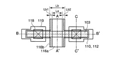
図1は第1の実施形態に係る半導体装置の基本的な構成を示した斜視図、図2は図1に示した半導体装置の平面図である。図3(a)は図2のA−A’に沿った断面図、図3(b)は図2のB−B’に沿った断面図、図3(c)は図2のC−C’に沿った断面図である。なお、図1では、構造の理解を容易にするため、ゲート電極を他の構造から離して描いているが、実際にはゲート電極は他の構造に接している。また、図1及び図3(a)〜図3(c)では、図2に示したコンタクトや配線等は描いていない。
図17は第2の実施形態に係る半導体装置の構成を示した斜視図、図18は図17に示した半導体装置の平面図である。図19(a)は図18のA−A’に沿った断面図、図19(b)は図18のB−B’に沿った断面図、図19(c)は図18のC−C’に沿った断面図、図19(d)は図18のD−D’に沿った断面図である。なお、図17では、構造の理解を容易にするため、ゲート電極を他の構造から離して描いているが、実際にはゲート電極は他の構造に接している。また、図17及び図19(a)〜図19(d)では、図18に示したコンタクトや配線等は描いていない。なお、本実施形態の基本的な構成は第1の実施形態と同様であり、第1の実施形態の構成要素に対応する構成要素については同一の参照番号を付し、それらの詳細な説明は省略する。
図20及び図21はいずれも、本実施形態に係る半導体装置の構成例を示した平面図である。図20に示した半導体装置の基本的な構成は第1の実施形態の構成に対応し、図21に示した半導体装置の基本的な構成は第2の実施形態の構成に対応している。したがって、各構成要素の詳細な説明は省略する。
図22及び図23はいずれも、本実施形態に係る半導体装置の構成例を示した平面図である。図22に示した半導体装置の基本的な構成は第1の実施形態の構成に対応し、図23に示した半導体装置の基本的な構成は第2の実施形態の構成に対応している。したがって、各構成要素の詳細な説明は省略する。
図24は、第1或いは第2の実施形態で示したようなトランジスタ構造をトレンチ型キャパシタ構造を有するDRAMに適用した場合の一例を示した断面図である。
図25は、第1或いは第2の実施形態で示したようなトランジスタ構造をスタック型キャパシタ構造を有するDRAMに適用した場合の一例を示した断面図である。
103…半導体構造 103a、103b、103c…半導体部分
104…熱酸化膜 105…シリコン窒化膜
106…ダミーゲート絶縁膜 108…ダミーゲート電極
109…シリコン酸化膜 110…シリコン窒化膜
111a…低濃度のソース領域 111b…低濃度のドレイン領域
112…シリコン酸化膜 113a…高濃度のソース領域
113b…高濃度のドレイン領域 114…層間絶縁膜
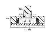
115…ゲート絶縁膜 116…ゲート電極
116a、116b…電極部分 117…層間絶縁膜
118…コンタクトプラグ 119…配線
120…凹部 151…熱酸化膜
161…レジストパターン
Claims (1)
- 下地絶縁膜上に、第1の半導体部分と、第2の半導体部分と、前記第1の半導体部分と第2の半導体部分との間の第3の半導体部分とを含む半導体構造を形成する工程と、
前記第3の半導体部分の上面及び側面を覆うダミー構造を形成する工程と、
前記ダミー構造をマスクとして前記半導体構造内に不純物のイオン注入を行い、ソース/ドレイン領域を形成する工程と、
前記第1の半導体部分の表面、前記第2の半導体部分の表面及び前記ダミー構造の側面を覆う絶縁部を形成する工程と、
前記ダミー構造を除去して、前記第3の半導体部分及び前記ダミー構造下の下地絶縁膜を露出させる工程と、
前記下地絶縁膜の露出した部分及び該露出した部分に隣接した部分をエッチングすることにより、前記下地絶縁膜に凹部を形成する工程と、
前記第3の半導体部分の上面及び側面を覆う第1の電極部分及び前記凹部内に形成された第2の電極部分を含むゲート電極を、前記第3の半導体部分と前記ゲート電極との間にゲート絶縁膜を介在させて形成する工程と、
を備えたことを特徴とする半導体装置の製造方法。
Priority Applications (3)
| Application Number | Priority Date | Filing Date | Title |
|---|---|---|---|
| JP2003407367A JP3962009B2 (ja) | 2003-12-05 | 2003-12-05 | 半導体装置の製造方法 |
| US10/874,732 US6992358B2 (en) | 2003-12-05 | 2004-06-24 | Semiconductor device and method for manufacturing the same |
| US11/289,279 US20060084215A1 (en) | 2003-12-05 | 2005-11-30 | Semiconductor device and method for manufacturing the same |
Applications Claiming Priority (1)
| Application Number | Priority Date | Filing Date | Title |
|---|---|---|---|
| JP2003407367A JP3962009B2 (ja) | 2003-12-05 | 2003-12-05 | 半導体装置の製造方法 |
Publications (2)
| Publication Number | Publication Date |
|---|---|
| JP2005167132A JP2005167132A (ja) | 2005-06-23 |
| JP3962009B2 true JP3962009B2 (ja) | 2007-08-22 |
Family
ID=34631749
Family Applications (1)
| Application Number | Title | Priority Date | Filing Date |
|---|---|---|---|
| JP2003407367A Expired - Fee Related JP3962009B2 (ja) | 2003-12-05 | 2003-12-05 | 半導体装置の製造方法 |
Country Status (2)
| Country | Link |
|---|---|
| US (2) | US6992358B2 (ja) |
| JP (1) | JP3962009B2 (ja) |
Families Citing this family (38)
| Publication number | Priority date | Publication date | Assignee | Title |
|---|---|---|---|---|
| JP2005243709A (ja) | 2004-02-24 | 2005-09-08 | Toshiba Corp | 半導体装置およびその製造方法 |
| JP4337983B2 (ja) * | 2005-02-17 | 2009-09-30 | 国立大学法人 東京大学 | 混在型半導体集積回路及びその製造方法 |
| US7176537B2 (en) * | 2005-05-23 | 2007-02-13 | Taiwan Semiconductor Manufacturing Company, Ltd. | High performance CMOS with metal-gate and Schottky source/drain |
| KR100608380B1 (ko) * | 2005-06-01 | 2006-08-08 | 주식회사 하이닉스반도체 | 메모리 소자의 트랜지스터 및 그 제조방법 |
| US7858481B2 (en) * | 2005-06-15 | 2010-12-28 | Intel Corporation | Method for fabricating transistor with thinned channel |
| US7348642B2 (en) * | 2005-08-03 | 2008-03-25 | International Business Machines Corporation | Fin-type field effect transistor |
| JP4954508B2 (ja) * | 2005-08-05 | 2012-06-20 | パナソニック株式会社 | 半導体装置 |
| KR100630764B1 (ko) | 2005-08-30 | 2006-10-04 | 삼성전자주식회사 | 게이트 올어라운드 반도체소자 및 그 제조방법 |
| EP1793366A3 (en) * | 2005-12-02 | 2009-11-04 | Semiconductor Energy Laboratory Co., Ltd. | Semiconductor device, display device, and electronic device |
| JP2007158269A (ja) | 2005-12-08 | 2007-06-21 | Elpida Memory Inc | 半導体装置及びその製造方法 |
| JP4525928B2 (ja) | 2005-12-27 | 2010-08-18 | セイコーエプソン株式会社 | 半導体装置の製造方法 |
| JP4496179B2 (ja) | 2006-03-13 | 2010-07-07 | 株式会社東芝 | 半導体記憶装置およびその製造方法 |
| JP5161495B2 (ja) * | 2006-07-19 | 2013-03-13 | 株式会社東芝 | 不揮発性半導体記憶装置 |
| US7906804B2 (en) | 2006-07-19 | 2011-03-15 | Kabushiki Kaisha Toshiba | Nonvolatile semiconductor memory device and manufacturing method thereof |
| JP2008300384A (ja) * | 2007-05-29 | 2008-12-11 | Elpida Memory Inc | 半導体装置及びその製造方法 |
| US8264048B2 (en) * | 2008-02-15 | 2012-09-11 | Intel Corporation | Multi-gate device having a T-shaped gate structure |
| WO2009110050A1 (ja) * | 2008-02-15 | 2009-09-11 | 日本ユニサンティスエレクトロニクス株式会社 | 半導体装置の製造方法 |
| FR2928029B1 (fr) * | 2008-02-27 | 2011-04-08 | St Microelectronics Crolles 2 | Procede de fabrication d'un dispositif semi-conducteur a grille enterree et circuit integre correspondant. |
| FR2928028B1 (fr) * | 2008-02-27 | 2011-07-15 | St Microelectronics Crolles 2 | Procede de fabrication d'un dispositif semi-conducteur a grille enterree et circuit integre correspondant. |
| US8410554B2 (en) | 2008-03-26 | 2013-04-02 | International Business Machines Corporation | Method, structure and design structure for customizing history effects of SOI circuits |
| US8420460B2 (en) | 2008-03-26 | 2013-04-16 | International Business Machines Corporation | Method, structure and design structure for customizing history effects of SOI circuits |
| US7964467B2 (en) * | 2008-03-26 | 2011-06-21 | International Business Machines Corporation | Method, structure and design structure for customizing history effects of soi circuits |
| US8399314B2 (en) * | 2010-03-25 | 2013-03-19 | International Business Machines Corporation | p-FET with a strained nanowire channel and embedded SiGe source and drain stressors |
| KR101774478B1 (ko) * | 2010-10-22 | 2017-09-05 | 삼성디스플레이 주식회사 | 박막 트랜지스터 및 그 제조 방법 |
| JP5325932B2 (ja) * | 2011-05-27 | 2013-10-23 | 株式会社東芝 | 半導体装置およびその製造方法 |
| KR101605643B1 (ko) | 2011-09-29 | 2016-03-22 | 인텔 코포레이션 | 반도체 응용을 위한 양전성 금속 포함 층을 포함하는 장치 및 그 제조방법 |
| US20130193513A1 (en) * | 2012-02-01 | 2013-08-01 | International Business Machines Corporation | Multi-Gate Field Effect Transistor with a Tapered Gate Profile |
| US9123654B2 (en) * | 2013-02-15 | 2015-09-01 | International Business Machines Corporation | Trilayer SIT process with transfer layer for FINFET patterning |
| US9385069B2 (en) * | 2013-03-07 | 2016-07-05 | Taiwan Semiconductor Manufacturing Company, Ltd. | Gate contact structure for FinFET |
| TWI644433B (zh) * | 2013-03-13 | 2018-12-11 | 半導體能源研究所股份有限公司 | 半導體裝置 |
| US10170315B2 (en) | 2013-07-17 | 2019-01-01 | Globalfoundries Inc. | Semiconductor device having local buried oxide |
| US9252272B2 (en) * | 2013-11-18 | 2016-02-02 | Globalfoundries Inc. | FinFET semiconductor device having local buried oxide |
| JP6204162B2 (ja) * | 2013-11-20 | 2017-09-27 | 猛英 白土 | 半導体装置及びその製造方法 |
| US9461050B2 (en) * | 2013-12-06 | 2016-10-04 | Globalfoundries Inc. | Self-aligned laterally extended strap for a dynamic random access memory cell |
| WO2015094244A1 (en) * | 2013-12-18 | 2015-06-25 | Intel Corporation | Techniques for improving gate control over transistor channel by increasing effective gate length |
| US9780213B2 (en) * | 2014-04-15 | 2017-10-03 | Taiwan Semiconductor Manufacturing Co., Ltd. | Semiconductor device having a reversed T-shaped profile in the metal gate line-end |
| US10636796B2 (en) * | 2017-08-02 | 2020-04-28 | Winbond Electronics Corp. | Dynamic random access memory and method of fabricating the same |
| CN108231594B (zh) * | 2017-12-21 | 2020-10-02 | 上海集成电路研发中心有限公司 | 一种FinFET器件的制作方法 |
Family Cites Families (19)
| Publication number | Priority date | Publication date | Assignee | Title |
|---|---|---|---|---|
| JP2582794B2 (ja) | 1987-08-10 | 1997-02-19 | 株式会社東芝 | 半導体装置及びその製造方法 |
| US6822071B1 (en) * | 1998-11-12 | 2004-11-23 | The Regents Of The University Of California | Polypeptides from Chlamydia pneumoniae and their use in the diagnosis, prevention and treatment of disease |
| US7242064B2 (en) * | 1999-06-30 | 2007-07-10 | Kabushiki Kaisha Toshiba | Semiconductor device and method of manufacturing the same |
| US6744390B1 (en) * | 2000-03-31 | 2004-06-01 | The Boeing Company | Analog to digital converter utilizing resolution enhancement |
| US20020011612A1 (en) * | 2000-07-31 | 2002-01-31 | Kabushiki Kaisha Toshiba | Semiconductor device and method for manufacturing the same |
| US6437404B1 (en) * | 2000-08-10 | 2002-08-20 | Advanced Micro Devices, Inc. | Semiconductor-on-insulator transistor with recessed source and drain |
| JP4216483B2 (ja) * | 2001-02-15 | 2009-01-28 | 株式会社東芝 | 半導体メモリ装置 |
| US6740938B2 (en) * | 2001-04-16 | 2004-05-25 | Semiconductor Energy Laboratory Co., Ltd. | Transistor provided with first and second gate electrodes with channel region therebetween |
| KR100363332B1 (en) * | 2001-05-23 | 2002-12-05 | Samsung Electronics Co Ltd | Method for forming semiconductor device having gate all-around type transistor |
| US6639246B2 (en) * | 2001-07-27 | 2003-10-28 | Semiconductor Energy Laboratory Co., Ltd. | Semiconductor device |
| JP2003188383A (ja) * | 2001-12-14 | 2003-07-04 | Hitachi Ltd | 半導体集積回路装置及びその製造方法 |
| JP3825688B2 (ja) * | 2001-12-25 | 2006-09-27 | 株式会社東芝 | 半導体装置の製造方法 |
| US6646307B1 (en) * | 2002-02-21 | 2003-11-11 | Advanced Micro Devices, Inc. | MOSFET having a double gate |
| US6580132B1 (en) * | 2002-04-10 | 2003-06-17 | International Business Machines Corporation | Damascene double-gate FET |
| JP2003332582A (ja) * | 2002-05-13 | 2003-11-21 | Toshiba Corp | 半導体装置及びその製造方法 |
| US7019644B2 (en) * | 2003-02-04 | 2006-03-28 | Barrie Robert P | Mobile object monitoring system |
| JP2005072093A (ja) * | 2003-08-20 | 2005-03-17 | Oki Electric Ind Co Ltd | 半導体装置 |
| JP4216676B2 (ja) * | 2003-09-08 | 2009-01-28 | 株式会社東芝 | 半導体装置 |
| US7091566B2 (en) * | 2003-11-20 | 2006-08-15 | International Business Machines Corp. | Dual gate FinFet |
-
2003
- 2003-12-05 JP JP2003407367A patent/JP3962009B2/ja not_active Expired - Fee Related
-
2004
- 2004-06-24 US US10/874,732 patent/US6992358B2/en not_active Expired - Fee Related
-
2005
- 2005-11-30 US US11/289,279 patent/US20060084215A1/en not_active Abandoned
Also Published As
| Publication number | Publication date |
|---|---|
| JP2005167132A (ja) | 2005-06-23 |
| US20060084215A1 (en) | 2006-04-20 |
| US6992358B2 (en) | 2006-01-31 |
| US20050121703A1 (en) | 2005-06-09 |
Similar Documents
| Publication | Publication Date | Title |
|---|---|---|
| JP3962009B2 (ja) | 半導体装置の製造方法 | |
| US7381601B2 (en) | Methods of fabricating field effect transistors having multiple stacked channels | |
| KR100605104B1 (ko) | 핀-펫 소자 및 그 제조 방법 | |
| JP2002118255A (ja) | 半導体装置およびその製造方法 | |
| US10325921B2 (en) | Semiconductor device and manufacturing method of the same | |
| US20020011612A1 (en) | Semiconductor device and method for manufacturing the same | |
| US20140038375A1 (en) | Semiconductor device having vertical mos transistor and method for manufacturing the semiconductor device | |
| KR100574340B1 (ko) | 반도체 장치 및 이의 형성 방법 | |
| TWI232002B (en) | Integrated metal-insulator-metal capacitor and metal gate transistor | |
| US8378395B2 (en) | Methods of fabricating field effect transistors having protruded active regions | |
| KR100668838B1 (ko) | 반도체 소자의 게이트 형성방법 | |
| JP2000332242A (ja) | 半導体装置及びその製造方法 | |
| US8013373B2 (en) | Semiconductor device having MOS-transistor formed on semiconductor substrate and method for manufacturing thereof | |
| US8748978B2 (en) | Sense-amp transistor of semiconductor device and method for manufacturing the same | |
| US7667266B2 (en) | Semiconductor device including active pattern with channel recess, and method of fabricating the same | |
| JP2009158813A (ja) | 半導体装置の製造方法、及び半導体装置 | |
| JP2012015345A (ja) | 半導体装置 | |
| JP2002359369A (ja) | 半導体装置の製造方法 | |
| TWI419266B (zh) | 半導體裝置之製造方法 | |
| US8264892B2 (en) | Semiconductor device and method of controlling the same | |
| US10818682B2 (en) | Method of manufacturing semiconductor device | |
| KR100629694B1 (ko) | 반도체 소자 제조 방법 | |
| TW202230728A (zh) | 半導體元件 | |
| JP2005136436A (ja) | 半導体装置およびその製造方法 | |
| JP2003197904A (ja) | 半導体装置および半導体装置の製造方法 |
Legal Events
| Date | Code | Title | Description |
|---|---|---|---|
| A977 | Report on retrieval |
Free format text: JAPANESE INTERMEDIATE CODE: A971007 Effective date: 20060828 |
|
| A131 | Notification of reasons for refusal |
Free format text: JAPANESE INTERMEDIATE CODE: A131 Effective date: 20060905 |
|
| A521 | Request for written amendment filed |
Free format text: JAPANESE INTERMEDIATE CODE: A523 Effective date: 20061027 |
|
| TRDD | Decision of grant or rejection written | ||
| A01 | Written decision to grant a patent or to grant a registration (utility model) |
Free format text: JAPANESE INTERMEDIATE CODE: A01 Effective date: 20070515 |
|
| A61 | First payment of annual fees (during grant procedure) |
Free format text: JAPANESE INTERMEDIATE CODE: A61 Effective date: 20070517 |
|
| FPAY | Renewal fee payment (event date is renewal date of database) |
Free format text: PAYMENT UNTIL: 20110525 Year of fee payment: 4 |
|
| LAPS | Cancellation because of no payment of annual fees |