JP2017123495A - Semiconductor device - Google Patents
Semiconductor device Download PDFInfo
- Publication number
- JP2017123495A JP2017123495A JP2017076490A JP2017076490A JP2017123495A JP 2017123495 A JP2017123495 A JP 2017123495A JP 2017076490 A JP2017076490 A JP 2017076490A JP 2017076490 A JP2017076490 A JP 2017076490A JP 2017123495 A JP2017123495 A JP 2017123495A
- Authority
- JP
- Japan
- Prior art keywords
- film
- oxide semiconductor
- oxide
- insulating film
- electrode layer
- Prior art date
- Legal status (The legal status is an assumption and is not a legal conclusion. Google has not performed a legal analysis and makes no representation as to the accuracy of the status listed.)
- Granted
Links
- 239000004065 semiconductor Substances 0.000 title claims abstract description 425
- TWNQGVIAIRXVLR-UHFFFAOYSA-N oxo(oxoalumanyloxy)alumane Chemical compound O=[Al]O[Al]=O TWNQGVIAIRXVLR-UHFFFAOYSA-N 0.000 claims abstract description 110
- 230000015572 biosynthetic process Effects 0.000 claims abstract description 65
- 239000002019 doping agent Substances 0.000 claims description 32
- 229910052738 indium Inorganic materials 0.000 claims description 10
- 229910052733 gallium Inorganic materials 0.000 claims description 9
- 229910052725 zinc Inorganic materials 0.000 claims description 7
- 238000009413 insulation Methods 0.000 abstract 3
- 239000010408 film Substances 0.000 description 744
- 239000010410 layer Substances 0.000 description 292
- 239000001301 oxygen Substances 0.000 description 116
- 229910052760 oxygen Inorganic materials 0.000 description 116
- QVGXLLKOCUKJST-UHFFFAOYSA-N atomic oxygen Chemical compound [O] QVGXLLKOCUKJST-UHFFFAOYSA-N 0.000 description 108
- 238000000034 method Methods 0.000 description 105
- 230000015654 memory Effects 0.000 description 70
- 239000000758 substrate Substances 0.000 description 54
- 239000000463 material Substances 0.000 description 52
- 239000011701 zinc Substances 0.000 description 44
- 238000010438 heat treatment Methods 0.000 description 38
- 239000012535 impurity Substances 0.000 description 36
- 238000004519 manufacturing process Methods 0.000 description 35
- 239000003990 capacitor Substances 0.000 description 34
- 239000011229 interlayer Substances 0.000 description 29
- IJGRMHOSHXDMSA-UHFFFAOYSA-N nitrogen Substances N#N IJGRMHOSHXDMSA-UHFFFAOYSA-N 0.000 description 29
- 239000013078 crystal Substances 0.000 description 23
- 229910052739 hydrogen Inorganic materials 0.000 description 22
- 238000005468 ion implantation Methods 0.000 description 22
- 238000004544 sputter deposition Methods 0.000 description 22
- 239000007789 gas Substances 0.000 description 21
- 239000001257 hydrogen Substances 0.000 description 21
- VYPSYNLAJGMNEJ-UHFFFAOYSA-N silicon dioxide Inorganic materials O=[Si]=O VYPSYNLAJGMNEJ-UHFFFAOYSA-N 0.000 description 21
- 230000006870 function Effects 0.000 description 20
- 229910052814 silicon oxide Inorganic materials 0.000 description 20
- 238000011282 treatment Methods 0.000 description 19
- 229910052751 metal Inorganic materials 0.000 description 18
- -1 oxygen radicals Chemical class 0.000 description 17
- XLOMVQKBTHCTTD-UHFFFAOYSA-N Zinc monoxide Chemical compound [Zn]=O XLOMVQKBTHCTTD-UHFFFAOYSA-N 0.000 description 16
- 150000002500 ions Chemical class 0.000 description 16
- 239000002184 metal Substances 0.000 description 16
- UFHFLCQGNIYNRP-UHFFFAOYSA-N Hydrogen Chemical compound [H][H] UFHFLCQGNIYNRP-UHFFFAOYSA-N 0.000 description 15
- 238000005530 etching Methods 0.000 description 15
- 229910052757 nitrogen Inorganic materials 0.000 description 15
- 239000000203 mixture Substances 0.000 description 14
- 238000005498 polishing Methods 0.000 description 14
- XKRFYHLGVUSROY-UHFFFAOYSA-N Argon Chemical compound [Ar] XKRFYHLGVUSROY-UHFFFAOYSA-N 0.000 description 12
- 229910052782 aluminium Inorganic materials 0.000 description 12
- XUIMIQQOPSSXEZ-UHFFFAOYSA-N Silicon Chemical compound [Si] XUIMIQQOPSSXEZ-UHFFFAOYSA-N 0.000 description 11
- 238000010586 diagram Methods 0.000 description 11
- 229910044991 metal oxide Inorganic materials 0.000 description 11
- 150000004706 metal oxides Chemical class 0.000 description 11
- 238000009832 plasma treatment Methods 0.000 description 11
- 230000008569 process Effects 0.000 description 11
- 229910052710 silicon Inorganic materials 0.000 description 11
- 239000010703 silicon Substances 0.000 description 11
- 229910052721 tungsten Inorganic materials 0.000 description 11
- GQPLMRYTRLFLPF-UHFFFAOYSA-N Nitrous Oxide Chemical compound [O-][N+]#N GQPLMRYTRLFLPF-UHFFFAOYSA-N 0.000 description 10
- XAGFODPZIPBFFR-UHFFFAOYSA-N aluminium Chemical compound [Al] XAGFODPZIPBFFR-UHFFFAOYSA-N 0.000 description 10
- 230000018044 dehydration Effects 0.000 description 10
- 238000006297 dehydration reaction Methods 0.000 description 10
- 238000006356 dehydrogenation reaction Methods 0.000 description 10
- 238000000151 deposition Methods 0.000 description 10
- XLYOFNOQVPJJNP-UHFFFAOYSA-N water Substances O XLYOFNOQVPJJNP-UHFFFAOYSA-N 0.000 description 10
- 229910001868 water Inorganic materials 0.000 description 10
- 229910052581 Si3N4 Inorganic materials 0.000 description 9
- 230000008021 deposition Effects 0.000 description 9
- 238000007654 immersion Methods 0.000 description 9
- 150000004767 nitrides Chemical class 0.000 description 9
- HQVNEWCFYHHQES-UHFFFAOYSA-N silicon nitride Chemical compound N12[Si]34N5[Si]62N3[Si]51N64 HQVNEWCFYHHQES-UHFFFAOYSA-N 0.000 description 9
- 239000000126 substance Substances 0.000 description 9
- 239000010936 titanium Substances 0.000 description 9
- 230000000903 blocking effect Effects 0.000 description 8
- 238000012545 processing Methods 0.000 description 8
- 239000002356 single layer Substances 0.000 description 8
- 229910052719 titanium Inorganic materials 0.000 description 8
- 239000010937 tungsten Substances 0.000 description 8
- 239000011787 zinc oxide Substances 0.000 description 8
- 239000010949 copper Substances 0.000 description 7
- PMHQVHHXPFUNSP-UHFFFAOYSA-M copper(1+);methylsulfanylmethane;bromide Chemical compound Br[Cu].CSC PMHQVHHXPFUNSP-UHFFFAOYSA-M 0.000 description 7
- 229910052750 molybdenum Inorganic materials 0.000 description 7
- 239000000843 powder Substances 0.000 description 7
- 238000005477 sputtering target Methods 0.000 description 7
- OAICVXFJPJFONN-UHFFFAOYSA-N Phosphorus Chemical compound [P] OAICVXFJPJFONN-UHFFFAOYSA-N 0.000 description 6
- 229910006404 SnO 2 Inorganic materials 0.000 description 6
- 229910052786 argon Inorganic materials 0.000 description 6
- 239000012298 atmosphere Substances 0.000 description 6
- 229910052802 copper Inorganic materials 0.000 description 6
- 230000007547 defect Effects 0.000 description 6
- 238000001312 dry etching Methods 0.000 description 6
- 150000002431 hydrogen Chemical class 0.000 description 6
- 229910003437 indium oxide Inorganic materials 0.000 description 6
- PJXISJQVUVHSOJ-UHFFFAOYSA-N indium(iii) oxide Chemical compound [O-2].[O-2].[O-2].[In+3].[In+3] PJXISJQVUVHSOJ-UHFFFAOYSA-N 0.000 description 6
- AMGQUBHHOARCQH-UHFFFAOYSA-N indium;oxotin Chemical compound [In].[Sn]=O AMGQUBHHOARCQH-UHFFFAOYSA-N 0.000 description 6
- 125000004430 oxygen atom Chemical group O* 0.000 description 6
- 239000002245 particle Substances 0.000 description 6
- 230000002093 peripheral effect Effects 0.000 description 6
- 229910052698 phosphorus Inorganic materials 0.000 description 6
- 239000011574 phosphorus Substances 0.000 description 6
- 239000003381 stabilizer Substances 0.000 description 6
- MYMOFIZGZYHOMD-UHFFFAOYSA-N Dioxygen Chemical compound O=O MYMOFIZGZYHOMD-UHFFFAOYSA-N 0.000 description 5
- NRTOMJZYCJJWKI-UHFFFAOYSA-N Titanium nitride Chemical compound [Ti]#N NRTOMJZYCJJWKI-UHFFFAOYSA-N 0.000 description 5
- 229910007541 Zn O Inorganic materials 0.000 description 5
- 238000003491 array Methods 0.000 description 5
- GPBUGPUPKAGMDK-UHFFFAOYSA-N azanylidynemolybdenum Chemical compound [Mo]#N GPBUGPUPKAGMDK-UHFFFAOYSA-N 0.000 description 5
- 239000011651 chromium Substances 0.000 description 5
- 150000001875 compounds Chemical class 0.000 description 5
- 229910001882 dioxygen Inorganic materials 0.000 description 5
- 229960001730 nitrous oxide Drugs 0.000 description 5
- 239000011368 organic material Substances 0.000 description 5
- 238000005268 plasma chemical vapour deposition Methods 0.000 description 5
- 230000004044 response Effects 0.000 description 5
- 238000003860 storage Methods 0.000 description 5
- YVTHLONGBIQYBO-UHFFFAOYSA-N zinc indium(3+) oxygen(2-) Chemical compound [O--].[Zn++].[In+3] YVTHLONGBIQYBO-UHFFFAOYSA-N 0.000 description 5
- RTAQQCXQSZGOHL-UHFFFAOYSA-N Titanium Chemical compound [Ti] RTAQQCXQSZGOHL-UHFFFAOYSA-N 0.000 description 4
- 229910052804 chromium Inorganic materials 0.000 description 4
- 230000005669 field effect Effects 0.000 description 4
- 229910052735 hafnium Inorganic materials 0.000 description 4
- 229910052734 helium Inorganic materials 0.000 description 4
- 239000001307 helium Substances 0.000 description 4
- SWQJXJOGLNCZEY-UHFFFAOYSA-N helium atom Chemical compound [He] SWQJXJOGLNCZEY-UHFFFAOYSA-N 0.000 description 4
- MRELNEQAGSRDBK-UHFFFAOYSA-N lanthanum(3+);oxygen(2-) Chemical compound [O-2].[O-2].[O-2].[La+3].[La+3] MRELNEQAGSRDBK-UHFFFAOYSA-N 0.000 description 4
- 230000001681 protective effect Effects 0.000 description 4
- 230000002441 reversible effect Effects 0.000 description 4
- 229910052715 tantalum Inorganic materials 0.000 description 4
- XOLBLPGZBRYERU-UHFFFAOYSA-N tin dioxide Chemical compound O=[Sn]=O XOLBLPGZBRYERU-UHFFFAOYSA-N 0.000 description 4
- 229910001887 tin oxide Inorganic materials 0.000 description 4
- QTBSBXVTEAMEQO-UHFFFAOYSA-N Acetic acid Chemical compound CC(O)=O QTBSBXVTEAMEQO-UHFFFAOYSA-N 0.000 description 3
- 229910018137 Al-Zn Inorganic materials 0.000 description 3
- 229910018573 Al—Zn Inorganic materials 0.000 description 3
- RYGMFSIKBFXOCR-UHFFFAOYSA-N Copper Chemical compound [Cu] RYGMFSIKBFXOCR-UHFFFAOYSA-N 0.000 description 3
- ZOKXTWBITQBERF-UHFFFAOYSA-N Molybdenum Chemical compound [Mo] ZOKXTWBITQBERF-UHFFFAOYSA-N 0.000 description 3
- 229910052779 Neodymium Inorganic materials 0.000 description 3
- 229910004298 SiO 2 Inorganic materials 0.000 description 3
- 229910020994 Sn-Zn Inorganic materials 0.000 description 3
- 229910009069 Sn—Zn Inorganic materials 0.000 description 3
- 239000000460 chlorine Substances 0.000 description 3
- 239000004020 conductor Substances 0.000 description 3
- 238000005520 cutting process Methods 0.000 description 3
- AJNVQOSZGJRYEI-UHFFFAOYSA-N digallium;oxygen(2-) Chemical compound [O-2].[O-2].[O-2].[Ga+3].[Ga+3] AJNVQOSZGJRYEI-UHFFFAOYSA-N 0.000 description 3
- 229910001195 gallium oxide Inorganic materials 0.000 description 3
- 238000000227 grinding Methods 0.000 description 3
- VBJZVLUMGGDVMO-UHFFFAOYSA-N hafnium atom Chemical compound [Hf] VBJZVLUMGGDVMO-UHFFFAOYSA-N 0.000 description 3
- 229910000449 hafnium oxide Inorganic materials 0.000 description 3
- WIHZLLGSGQNAGK-UHFFFAOYSA-N hafnium(4+);oxygen(2-) Chemical compound [O-2].[O-2].[Hf+4] WIHZLLGSGQNAGK-UHFFFAOYSA-N 0.000 description 3
- 125000002887 hydroxy group Chemical group [H]O* 0.000 description 3
- 238000002513 implantation Methods 0.000 description 3
- APFVFJFRJDLVQX-UHFFFAOYSA-N indium atom Chemical compound [In] APFVFJFRJDLVQX-UHFFFAOYSA-N 0.000 description 3
- 238000009616 inductively coupled plasma Methods 0.000 description 3
- 239000011261 inert gas Substances 0.000 description 3
- 230000010354 integration Effects 0.000 description 3
- 239000007769 metal material Substances 0.000 description 3
- 239000011733 molybdenum Substances 0.000 description 3
- QEFYFXOXNSNQGX-UHFFFAOYSA-N neodymium atom Chemical compound [Nd] QEFYFXOXNSNQGX-UHFFFAOYSA-N 0.000 description 3
- 229910052754 neon Inorganic materials 0.000 description 3
- GKAOGPIIYCISHV-UHFFFAOYSA-N neon atom Chemical compound [Ne] GKAOGPIIYCISHV-UHFFFAOYSA-N 0.000 description 3
- 239000012299 nitrogen atmosphere Substances 0.000 description 3
- 235000013842 nitrous oxide Nutrition 0.000 description 3
- 230000003746 surface roughness Effects 0.000 description 3
- JBQYATWDVHIOAR-UHFFFAOYSA-N tellanylidenegermanium Chemical compound [Te]=[Ge] JBQYATWDVHIOAR-UHFFFAOYSA-N 0.000 description 3
- 239000010409 thin film Substances 0.000 description 3
- WFKWXMTUELFFGS-UHFFFAOYSA-N tungsten Chemical compound [W] WFKWXMTUELFFGS-UHFFFAOYSA-N 0.000 description 3
- 238000001039 wet etching Methods 0.000 description 3
- 229910018120 Al-Ga-Zn Inorganic materials 0.000 description 2
- CURLTUGMZLYLDI-UHFFFAOYSA-N Carbon dioxide Chemical compound O=C=O CURLTUGMZLYLDI-UHFFFAOYSA-N 0.000 description 2
- VYZAMTAEIAYCRO-UHFFFAOYSA-N Chromium Chemical compound [Cr] VYZAMTAEIAYCRO-UHFFFAOYSA-N 0.000 description 2
- GYHNNYVSQQEPJS-UHFFFAOYSA-N Gallium Chemical compound [Ga] GYHNNYVSQQEPJS-UHFFFAOYSA-N 0.000 description 2
- BPQQTUXANYXVAA-UHFFFAOYSA-N Orthosilicate Chemical compound [O-][Si]([O-])([O-])[O-] BPQQTUXANYXVAA-UHFFFAOYSA-N 0.000 description 2
- NBIIXXVUZAFLBC-UHFFFAOYSA-N Phosphoric acid Chemical compound OP(O)(O)=O NBIIXXVUZAFLBC-UHFFFAOYSA-N 0.000 description 2
- 239000004642 Polyimide Substances 0.000 description 2
- 229910000577 Silicon-germanium Inorganic materials 0.000 description 2
- 229910020868 Sn-Ga-Zn Inorganic materials 0.000 description 2
- ATJFFYVFTNAWJD-UHFFFAOYSA-N Tin Chemical compound [Sn] ATJFFYVFTNAWJD-UHFFFAOYSA-N 0.000 description 2
- GWEVSGVZZGPLCZ-UHFFFAOYSA-N Titan oxide Chemical compound O=[Ti]=O GWEVSGVZZGPLCZ-UHFFFAOYSA-N 0.000 description 2
- LEVVHYCKPQWKOP-UHFFFAOYSA-N [Si].[Ge] Chemical compound [Si].[Ge] LEVVHYCKPQWKOP-UHFFFAOYSA-N 0.000 description 2
- 230000001133 acceleration Effects 0.000 description 2
- 239000012300 argon atmosphere Substances 0.000 description 2
- 125000004429 atom Chemical group 0.000 description 2
- QVQLCTNNEUAWMS-UHFFFAOYSA-N barium oxide Chemical compound [Ba]=O QVQLCTNNEUAWMS-UHFFFAOYSA-N 0.000 description 2
- UMIVXZPTRXBADB-UHFFFAOYSA-N benzocyclobutene Chemical compound C1=CC=C2CCC2=C1 UMIVXZPTRXBADB-UHFFFAOYSA-N 0.000 description 2
- 230000005540 biological transmission Effects 0.000 description 2
- 229910052799 carbon Inorganic materials 0.000 description 2
- 230000008859 change Effects 0.000 description 2
- 238000005229 chemical vapour deposition Methods 0.000 description 2
- 238000002425 crystallisation Methods 0.000 description 2
- 230000008025 crystallization Effects 0.000 description 2
- 230000006866 deterioration Effects 0.000 description 2
- 150000004678 hydrides Chemical class 0.000 description 2
- 125000004435 hydrogen atom Chemical group [H]* 0.000 description 2
- 230000005012 migration Effects 0.000 description 2
- 238000013508 migration Methods 0.000 description 2
- 238000002156 mixing Methods 0.000 description 2
- 239000001272 nitrous oxide Substances 0.000 description 2
- QGLKJKCYBOYXKC-UHFFFAOYSA-N nonaoxidotritungsten Chemical compound O=[W]1(=O)O[W](=O)(=O)O[W](=O)(=O)O1 QGLKJKCYBOYXKC-UHFFFAOYSA-N 0.000 description 2
- 229920001721 polyimide Polymers 0.000 description 2
- 230000005855 radiation Effects 0.000 description 2
- 239000003870 refractory metal Substances 0.000 description 2
- 239000011347 resin Substances 0.000 description 2
- 229920005989 resin Polymers 0.000 description 2
- 238000005001 rutherford backscattering spectroscopy Methods 0.000 description 2
- 229910052706 scandium Inorganic materials 0.000 description 2
- SIXSYDAISGFNSX-UHFFFAOYSA-N scandium atom Chemical compound [Sc] SIXSYDAISGFNSX-UHFFFAOYSA-N 0.000 description 2
- HBMJWWWQQXIZIP-UHFFFAOYSA-N silicon carbide Chemical compound [Si+]#[C-] HBMJWWWQQXIZIP-UHFFFAOYSA-N 0.000 description 2
- 229910010271 silicon carbide Inorganic materials 0.000 description 2
- 238000001179 sorption measurement Methods 0.000 description 2
- GUVRBAGPIYLISA-UHFFFAOYSA-N tantalum atom Chemical compound [Ta] GUVRBAGPIYLISA-UHFFFAOYSA-N 0.000 description 2
- MZLGASXMSKOWSE-UHFFFAOYSA-N tantalum nitride Chemical compound [Ta]#N MZLGASXMSKOWSE-UHFFFAOYSA-N 0.000 description 2
- OGIDPMRJRNCKJF-UHFFFAOYSA-N titanium oxide Inorganic materials [Ti]=O OGIDPMRJRNCKJF-UHFFFAOYSA-N 0.000 description 2
- 229910001930 tungsten oxide Inorganic materials 0.000 description 2
- 239000004925 Acrylic resin Substances 0.000 description 1
- 229920000178 Acrylic resin Polymers 0.000 description 1
- JBRZTFJDHDCESZ-UHFFFAOYSA-N AsGa Chemical compound [As]#[Ga] JBRZTFJDHDCESZ-UHFFFAOYSA-N 0.000 description 1
- ZOXJGFHDIHLPTG-UHFFFAOYSA-N Boron Chemical compound [B] ZOXJGFHDIHLPTG-UHFFFAOYSA-N 0.000 description 1
- OKTJSMMVPCPJKN-UHFFFAOYSA-N Carbon Chemical compound [C] OKTJSMMVPCPJKN-UHFFFAOYSA-N 0.000 description 1
- 229910052684 Cerium Inorganic materials 0.000 description 1
- VEXZGXHMUGYJMC-UHFFFAOYSA-M Chloride anion Chemical compound [Cl-] VEXZGXHMUGYJMC-UHFFFAOYSA-M 0.000 description 1
- ZAMOUSCENKQFHK-UHFFFAOYSA-N Chlorine atom Chemical compound [Cl] ZAMOUSCENKQFHK-UHFFFAOYSA-N 0.000 description 1
- 229910052692 Dysprosium Inorganic materials 0.000 description 1
- 229910052691 Erbium Inorganic materials 0.000 description 1
- 229910052693 Europium Inorganic materials 0.000 description 1
- KRHYYFGTRYWZRS-UHFFFAOYSA-M Fluoride anion Chemical compound [F-] KRHYYFGTRYWZRS-UHFFFAOYSA-M 0.000 description 1
- PXGOKWXKJXAPGV-UHFFFAOYSA-N Fluorine Chemical compound FF PXGOKWXKJXAPGV-UHFFFAOYSA-N 0.000 description 1
- 229910052688 Gadolinium Inorganic materials 0.000 description 1
- 229910001218 Gallium arsenide Inorganic materials 0.000 description 1
- 229910004129 HfSiO Inorganic materials 0.000 description 1
- 229910052689 Holmium Inorganic materials 0.000 description 1
- DGAQECJNVWCQMB-PUAWFVPOSA-M Ilexoside XXIX Chemical compound C[C@@H]1CC[C@@]2(CC[C@@]3(C(=CC[C@H]4[C@]3(CC[C@@H]5[C@@]4(CC[C@@H](C5(C)C)OS(=O)(=O)[O-])C)C)[C@@H]2[C@]1(C)O)C)C(=O)O[C@H]6[C@@H]([C@H]([C@@H]([C@H](O6)CO)O)O)O.[Na+] DGAQECJNVWCQMB-PUAWFVPOSA-M 0.000 description 1
- 108010083687 Ion Pumps Proteins 0.000 description 1
- 229910052765 Lutetium Inorganic materials 0.000 description 1
- GRYLNZFGIOXLOG-UHFFFAOYSA-N Nitric acid Chemical compound O[N+]([O-])=O GRYLNZFGIOXLOG-UHFFFAOYSA-N 0.000 description 1
- 229910052777 Praseodymium Inorganic materials 0.000 description 1
- 229910052772 Samarium Inorganic materials 0.000 description 1
- 229910020833 Sn-Al-Zn Inorganic materials 0.000 description 1
- 229910020944 Sn-Mg Inorganic materials 0.000 description 1
- 229910020923 Sn-O Inorganic materials 0.000 description 1
- 229910052771 Terbium Inorganic materials 0.000 description 1
- 229910052775 Thulium Inorganic materials 0.000 description 1
- 238000000560 X-ray reflectometry Methods 0.000 description 1
- 229910052769 Ytterbium Inorganic materials 0.000 description 1
- 229910009369 Zn Mg Inorganic materials 0.000 description 1
- 229910007573 Zn-Mg Inorganic materials 0.000 description 1
- NIXOWILDQLNWCW-UHFFFAOYSA-N acrylic acid group Chemical group C(C=C)(=O)O NIXOWILDQLNWCW-UHFFFAOYSA-N 0.000 description 1
- 230000009471 action Effects 0.000 description 1
- 239000000956 alloy Substances 0.000 description 1
- 229910000147 aluminium phosphate Inorganic materials 0.000 description 1
- 239000005407 aluminoborosilicate glass Substances 0.000 description 1
- 229910052787 antimony Inorganic materials 0.000 description 1
- WATWJIUSRGPENY-UHFFFAOYSA-N antimony atom Chemical compound [Sb] WATWJIUSRGPENY-UHFFFAOYSA-N 0.000 description 1
- 229910052785 arsenic Inorganic materials 0.000 description 1
- RQNWIZPPADIBDY-UHFFFAOYSA-N arsenic atom Chemical compound [As] RQNWIZPPADIBDY-UHFFFAOYSA-N 0.000 description 1
- 229910052788 barium Inorganic materials 0.000 description 1
- DSAJWYNOEDNPEQ-UHFFFAOYSA-N barium atom Chemical compound [Ba] DSAJWYNOEDNPEQ-UHFFFAOYSA-N 0.000 description 1
- 229910052796 boron Inorganic materials 0.000 description 1
- 239000005388 borosilicate glass Substances 0.000 description 1
- 150000001721 carbon Chemical group 0.000 description 1
- 239000001569 carbon dioxide Substances 0.000 description 1
- 229910002092 carbon dioxide Inorganic materials 0.000 description 1
- 239000000919 ceramic Substances 0.000 description 1
- GWXLDORMOJMVQZ-UHFFFAOYSA-N cerium Chemical compound [Ce] GWXLDORMOJMVQZ-UHFFFAOYSA-N 0.000 description 1
- 229910052801 chlorine Inorganic materials 0.000 description 1
- 238000013461 design Methods 0.000 description 1
- 238000009826 distribution Methods 0.000 description 1
- 230000009977 dual effect Effects 0.000 description 1
- 239000000428 dust Substances 0.000 description 1
- KBQHZAAAGSGFKK-UHFFFAOYSA-N dysprosium atom Chemical compound [Dy] KBQHZAAAGSGFKK-UHFFFAOYSA-N 0.000 description 1
- UYAHIZSMUZPPFV-UHFFFAOYSA-N erbium Chemical compound [Er] UYAHIZSMUZPPFV-UHFFFAOYSA-N 0.000 description 1
- OGPBJKLSAFTDLK-UHFFFAOYSA-N europium atom Chemical compound [Eu] OGPBJKLSAFTDLK-UHFFFAOYSA-N 0.000 description 1
- 238000001704 evaporation Methods 0.000 description 1
- 238000011049 filling Methods 0.000 description 1
- 229910052731 fluorine Inorganic materials 0.000 description 1
- 239000011737 fluorine Substances 0.000 description 1
- UIWYJDYFSGRHKR-UHFFFAOYSA-N gadolinium atom Chemical compound [Gd] UIWYJDYFSGRHKR-UHFFFAOYSA-N 0.000 description 1
- 229910052732 germanium Inorganic materials 0.000 description 1
- GNPVGFCGXDBREM-UHFFFAOYSA-N germanium atom Chemical compound [Ge] GNPVGFCGXDBREM-UHFFFAOYSA-N 0.000 description 1
- 239000011521 glass Substances 0.000 description 1
- 229910052736 halogen Inorganic materials 0.000 description 1
- 150000002367 halogens Chemical class 0.000 description 1
- KJZYNXUDTRRSPN-UHFFFAOYSA-N holmium atom Chemical compound [Ho] KJZYNXUDTRRSPN-UHFFFAOYSA-N 0.000 description 1
- 229910000765 intermetallic Inorganic materials 0.000 description 1
- 229910052742 iron Inorganic materials 0.000 description 1
- 238000002955 isolation Methods 0.000 description 1
- 238000003475 lamination Methods 0.000 description 1
- 229910052747 lanthanoid Inorganic materials 0.000 description 1
- 150000002602 lanthanoids Chemical class 0.000 description 1
- 229910052746 lanthanum Inorganic materials 0.000 description 1
- FZLIPJUXYLNCLC-UHFFFAOYSA-N lanthanum atom Chemical compound [La] FZLIPJUXYLNCLC-UHFFFAOYSA-N 0.000 description 1
- 238000001307 laser spectroscopy Methods 0.000 description 1
- 239000004973 liquid crystal related substance Substances 0.000 description 1
- 230000007774 longterm Effects 0.000 description 1
- OHSVLFRHMCKCQY-UHFFFAOYSA-N lutetium atom Chemical compound [Lu] OHSVLFRHMCKCQY-UHFFFAOYSA-N 0.000 description 1
- 239000011777 magnesium Substances 0.000 description 1
- 239000000395 magnesium oxide Substances 0.000 description 1
- CPLXHLVBOLITMK-UHFFFAOYSA-N magnesium oxide Inorganic materials [Mg]=O CPLXHLVBOLITMK-UHFFFAOYSA-N 0.000 description 1
- AXZKOIWUVFPNLO-UHFFFAOYSA-N magnesium;oxygen(2-) Chemical compound [O-2].[Mg+2] AXZKOIWUVFPNLO-UHFFFAOYSA-N 0.000 description 1
- 229910052748 manganese Inorganic materials 0.000 description 1
- 238000004949 mass spectrometry Methods 0.000 description 1
- 238000000691 measurement method Methods 0.000 description 1
- 239000012528 membrane Substances 0.000 description 1
- QSHDDOUJBYECFT-UHFFFAOYSA-N mercury Chemical compound [Hg] QSHDDOUJBYECFT-UHFFFAOYSA-N 0.000 description 1
- 229910052753 mercury Inorganic materials 0.000 description 1
- 229910001507 metal halide Inorganic materials 0.000 description 1
- 150000005309 metal halides Chemical class 0.000 description 1
- 150000002739 metals Chemical class 0.000 description 1
- 239000011259 mixed solution Substances 0.000 description 1
- 229910021334 nickel silicide Inorganic materials 0.000 description 1
- RUFLMLWJRZAWLJ-UHFFFAOYSA-N nickel silicide Chemical compound [Ni]=[Si]=[Ni] RUFLMLWJRZAWLJ-UHFFFAOYSA-N 0.000 description 1
- 229910017604 nitric acid Inorganic materials 0.000 description 1
- QJGQUHMNIGDVPM-UHFFFAOYSA-N nitrogen group Chemical group [N] QJGQUHMNIGDVPM-UHFFFAOYSA-N 0.000 description 1
- 230000003647 oxidation Effects 0.000 description 1
- 238000007254 oxidation reaction Methods 0.000 description 1
- SIWVEOZUMHYXCS-UHFFFAOYSA-N oxo(oxoyttriooxy)yttrium Chemical compound O=[Y]O[Y]=O SIWVEOZUMHYXCS-UHFFFAOYSA-N 0.000 description 1
- RVTZCBVAJQQJTK-UHFFFAOYSA-N oxygen(2-);zirconium(4+) Chemical compound [O-2].[O-2].[Zr+4] RVTZCBVAJQQJTK-UHFFFAOYSA-N 0.000 description 1
- 238000000206 photolithography Methods 0.000 description 1
- 229910052696 pnictogen Inorganic materials 0.000 description 1
- 229910021420 polycrystalline silicon Inorganic materials 0.000 description 1
- PUDIUYLPXJFUGB-UHFFFAOYSA-N praseodymium atom Chemical compound [Pr] PUDIUYLPXJFUGB-UHFFFAOYSA-N 0.000 description 1
- 238000004549 pulsed laser deposition Methods 0.000 description 1
- 239000010453 quartz Substances 0.000 description 1
- 230000009467 reduction Effects 0.000 description 1
- 230000000717 retained effect Effects 0.000 description 1
- 238000004439 roughness measurement Methods 0.000 description 1
- KZUNJOHGWZRPMI-UHFFFAOYSA-N samarium atom Chemical compound [Sm] KZUNJOHGWZRPMI-UHFFFAOYSA-N 0.000 description 1
- 229910052594 sapphire Inorganic materials 0.000 description 1
- 239000010980 sapphire Substances 0.000 description 1
- VSZWPYCFIRKVQL-UHFFFAOYSA-N selanylidenegallium;selenium Chemical compound [Se].[Se]=[Ga].[Se]=[Ga] VSZWPYCFIRKVQL-UHFFFAOYSA-N 0.000 description 1
- 238000000926 separation method Methods 0.000 description 1
- 229910021332 silicide Inorganic materials 0.000 description 1
- FVBUAEGBCNSCDD-UHFFFAOYSA-N silicide(4-) Chemical compound [Si-4] FVBUAEGBCNSCDD-UHFFFAOYSA-N 0.000 description 1
- 239000011734 sodium Substances 0.000 description 1
- 229910052708 sodium Inorganic materials 0.000 description 1
- 238000004611 spectroscopical analysis Methods 0.000 description 1
- 238000004528 spin coating Methods 0.000 description 1
- 238000000859 sublimation Methods 0.000 description 1
- 230000008022 sublimation Effects 0.000 description 1
- GZCRRIHWUXGPOV-UHFFFAOYSA-N terbium atom Chemical compound [Tb] GZCRRIHWUXGPOV-UHFFFAOYSA-N 0.000 description 1
- FRNOGLGSGLTDKL-UHFFFAOYSA-N thulium atom Chemical compound [Tm] FRNOGLGSGLTDKL-UHFFFAOYSA-N 0.000 description 1
- 238000012546 transfer Methods 0.000 description 1
- 229910052720 vanadium Inorganic materials 0.000 description 1
- 229910052724 xenon Inorganic materials 0.000 description 1
- FHNFHKCVQCLJFQ-UHFFFAOYSA-N xenon atom Chemical compound [Xe] FHNFHKCVQCLJFQ-UHFFFAOYSA-N 0.000 description 1
- NAWDYIZEMPQZHO-UHFFFAOYSA-N ytterbium Chemical compound [Yb] NAWDYIZEMPQZHO-UHFFFAOYSA-N 0.000 description 1
- 229910001928 zirconium oxide Inorganic materials 0.000 description 1
Images


Classifications
-
- H—ELECTRICITY
- H01—ELECTRIC ELEMENTS
- H01L—SEMICONDUCTOR DEVICES NOT COVERED BY CLASS H10
- H01L29/00—Semiconductor devices adapted for rectifying, amplifying, oscillating or switching, or capacitors or resistors with at least one potential-jump barrier or surface barrier, e.g. PN junction depletion layer or carrier concentration layer; Details of semiconductor bodies or of electrodes thereof ; Multistep manufacturing processes therefor
- H01L29/66—Types of semiconductor device ; Multistep manufacturing processes therefor
- H01L29/68—Types of semiconductor device ; Multistep manufacturing processes therefor controllable by only the electric current supplied, or only the electric potential applied, to an electrode which does not carry the current to be rectified, amplified or switched
- H01L29/76—Unipolar devices, e.g. field effect transistors
- H01L29/772—Field effect transistors
- H01L29/78—Field effect transistors with field effect produced by an insulated gate
- H01L29/786—Thin film transistors, i.e. transistors with a channel being at least partly a thin film
- H01L29/78606—Thin film transistors, i.e. transistors with a channel being at least partly a thin film with supplementary region or layer in the thin film or in the insulated bulk substrate supporting it for controlling or increasing the safety of the device
-
- H—ELECTRICITY
- H01—ELECTRIC ELEMENTS
- H01L—SEMICONDUCTOR DEVICES NOT COVERED BY CLASS H10
- H01L29/00—Semiconductor devices adapted for rectifying, amplifying, oscillating or switching, or capacitors or resistors with at least one potential-jump barrier or surface barrier, e.g. PN junction depletion layer or carrier concentration layer; Details of semiconductor bodies or of electrodes thereof ; Multistep manufacturing processes therefor
- H01L29/40—Electrodes ; Multistep manufacturing processes therefor
- H01L29/41—Electrodes ; Multistep manufacturing processes therefor characterised by their shape, relative sizes or dispositions
- H01L29/417—Electrodes ; Multistep manufacturing processes therefor characterised by their shape, relative sizes or dispositions carrying the current to be rectified, amplified or switched
- H01L29/41725—Source or drain electrodes for field effect devices
- H01L29/41733—Source or drain electrodes for field effect devices for thin film transistors with insulated gate
-
- H—ELECTRICITY
- H01—ELECTRIC ELEMENTS
- H01L—SEMICONDUCTOR DEVICES NOT COVERED BY CLASS H10
- H01L29/00—Semiconductor devices adapted for rectifying, amplifying, oscillating or switching, or capacitors or resistors with at least one potential-jump barrier or surface barrier, e.g. PN junction depletion layer or carrier concentration layer; Details of semiconductor bodies or of electrodes thereof ; Multistep manufacturing processes therefor
- H01L29/66—Types of semiconductor device ; Multistep manufacturing processes therefor
- H01L29/66007—Multistep manufacturing processes
- H01L29/66075—Multistep manufacturing processes of devices having semiconductor bodies comprising group 14 or group 13/15 materials
- H01L29/66227—Multistep manufacturing processes of devices having semiconductor bodies comprising group 14 or group 13/15 materials the devices being controllable only by the electric current supplied or the electric potential applied, to an electrode which does not carry the current to be rectified, amplified or switched, e.g. three-terminal devices
- H01L29/66409—Unipolar field-effect transistors
- H01L29/66477—Unipolar field-effect transistors with an insulated gate, i.e. MISFET
- H01L29/66742—Thin film unipolar transistors
-
- H—ELECTRICITY
- H01—ELECTRIC ELEMENTS
- H01L—SEMICONDUCTOR DEVICES NOT COVERED BY CLASS H10
- H01L29/00—Semiconductor devices adapted for rectifying, amplifying, oscillating or switching, or capacitors or resistors with at least one potential-jump barrier or surface barrier, e.g. PN junction depletion layer or carrier concentration layer; Details of semiconductor bodies or of electrodes thereof ; Multistep manufacturing processes therefor
- H01L29/66—Types of semiconductor device ; Multistep manufacturing processes therefor
- H01L29/66007—Multistep manufacturing processes
- H01L29/66969—Multistep manufacturing processes of devices having semiconductor bodies not comprising group 14 or group 13/15 materials
-
- H—ELECTRICITY
- H01—ELECTRIC ELEMENTS
- H01L—SEMICONDUCTOR DEVICES NOT COVERED BY CLASS H10
- H01L29/00—Semiconductor devices adapted for rectifying, amplifying, oscillating or switching, or capacitors or resistors with at least one potential-jump barrier or surface barrier, e.g. PN junction depletion layer or carrier concentration layer; Details of semiconductor bodies or of electrodes thereof ; Multistep manufacturing processes therefor
- H01L29/66—Types of semiconductor device ; Multistep manufacturing processes therefor
- H01L29/68—Types of semiconductor device ; Multistep manufacturing processes therefor controllable by only the electric current supplied, or only the electric potential applied, to an electrode which does not carry the current to be rectified, amplified or switched
- H01L29/76—Unipolar devices, e.g. field effect transistors
- H01L29/772—Field effect transistors
- H01L29/78—Field effect transistors with field effect produced by an insulated gate
- H01L29/786—Thin film transistors, i.e. transistors with a channel being at least partly a thin film
- H01L29/7869—Thin film transistors, i.e. transistors with a channel being at least partly a thin film having a semiconductor body comprising an oxide semiconductor material, e.g. zinc oxide, copper aluminium oxide, cadmium stannate
-
- H—ELECTRICITY
- H01—ELECTRIC ELEMENTS
- H01L—SEMICONDUCTOR DEVICES NOT COVERED BY CLASS H10
- H01L29/00—Semiconductor devices adapted for rectifying, amplifying, oscillating or switching, or capacitors or resistors with at least one potential-jump barrier or surface barrier, e.g. PN junction depletion layer or carrier concentration layer; Details of semiconductor bodies or of electrodes thereof ; Multistep manufacturing processes therefor
- H01L29/66—Types of semiconductor device ; Multistep manufacturing processes therefor
- H01L29/68—Types of semiconductor device ; Multistep manufacturing processes therefor controllable by only the electric current supplied, or only the electric potential applied, to an electrode which does not carry the current to be rectified, amplified or switched
- H01L29/76—Unipolar devices, e.g. field effect transistors
- H01L29/772—Field effect transistors
- H01L29/78—Field effect transistors with field effect produced by an insulated gate
- H01L29/786—Thin film transistors, i.e. transistors with a channel being at least partly a thin film
- H01L29/78696—Thin film transistors, i.e. transistors with a channel being at least partly a thin film characterised by the structure of the channel, e.g. multichannel, transverse or longitudinal shape, length or width, doping structure, or the overlap or alignment between the channel and the gate, the source or the drain, or the contacting structure of the channel
-
- H—ELECTRICITY
- H10—SEMICONDUCTOR DEVICES; ELECTRIC SOLID-STATE DEVICES NOT OTHERWISE PROVIDED FOR
- H10B—ELECTRONIC MEMORY DEVICES
- H10B41/00—Electrically erasable-and-programmable ROM [EEPROM] devices comprising floating gates
- H10B41/70—Electrically erasable-and-programmable ROM [EEPROM] devices comprising floating gates the floating gate being an electrode shared by two or more components
Landscapes
- Engineering & Computer Science (AREA)
- Microelectronics & Electronic Packaging (AREA)
- Power Engineering (AREA)
- Physics & Mathematics (AREA)
- Ceramic Engineering (AREA)
- Condensed Matter Physics & Semiconductors (AREA)
- General Physics & Mathematics (AREA)
- Computer Hardware Design (AREA)
- Manufacturing & Machinery (AREA)
- Semiconductor Memories (AREA)
- Thin Film Transistor (AREA)
- Electrodes Of Semiconductors (AREA)
- Non-Volatile Memory (AREA)
- Metal-Oxide And Bipolar Metal-Oxide Semiconductor Integrated Circuits (AREA)
- Devices For Indicating Variable Information By Combining Individual Elements (AREA)
- Physical Vapour Deposition (AREA)
Abstract
Description
半導体装置及び半導体装置の作製方法に関する。 The present invention relates to a semiconductor device and a method for manufacturing the semiconductor device.
なお、本明細書中において半導体装置とは、半導体特性を利用することで機能しうる装置
全般を指し、電気光学装置、半導体回路および電子機器は全て半導体装置である。
Note that in this specification, a semiconductor device refers to all devices that can function by utilizing semiconductor characteristics, and an electro-optical device, a semiconductor circuit, and an electronic device are all semiconductor devices.
絶縁表面を有する基板上に形成された半導体薄膜を用いてトランジスタ(薄膜トランジス
タ(TFT)ともいう)を構成する技術が注目されている。該トランジスタは集積回路(
IC)や画像表示装置(表示装置)のような電子デバイスに広く応用されている。トラン
ジスタに適用可能な半導体薄膜としてシリコン系半導体材料が広く知られているが、その
他の材料として酸化物半導体が注目されている。
A technique for forming a transistor (also referred to as a thin film transistor (TFT)) using a semiconductor thin film formed over a substrate having an insulating surface has attracted attention. The transistor is an integrated circuit (
IC) and electronic devices such as image display devices (display devices). A silicon-based semiconductor material is widely known as a semiconductor thin film applicable to a transistor, but an oxide semiconductor has attracted attention as another material.
例えば、インジウム(In)、ガリウム(Ga)、及び亜鉛(Zn)を含むアモルファス
酸化物(In−Ga−Zn−O系アモルファス酸化物)からなる半導体層を用いたトラン
ジスタが開示されている(特許文献1参照)。
For example, a transistor using a semiconductor layer made of an amorphous oxide (In—Ga—Zn—O-based amorphous oxide) containing indium (In), gallium (Ga), and zinc (Zn) is disclosed (patent) Reference 1).
ところで、トランジスタの動作の高速化、トランジスタの低消費電力化、高集積化等を達
成するためにはトランジスタの微細化が必須である。
By the way, miniaturization of a transistor is indispensable in order to achieve high-speed operation of the transistor, low power consumption of the transistor, high integration, and the like.
より高性能な半導体装置を実現するため、微細化されたトランジスタのオン特性(例えば
、オン電流や電界効果移動度)を向上させて、半導体装置の高速応答、高速駆動を実現す
る構成およびその作製方法を提供することを目的の一とする。
In order to realize a higher-performance semiconductor device, the on-characteristics of a miniaturized transistor (for example, on-current and field-effect mobility) are improved to realize a high-speed response and high-speed driving of the semiconductor device and its manufacture An object is to provide a method.
また、トランジスタの微細化に伴って作製工程における歩留まりの低下が懸念される。 In addition, there is a concern that the yield in the manufacturing process may decrease with the miniaturization of the transistor.
微細な構造であっても高い電気的特性及び信頼性を有するトランジスタを歩留まりよく提
供することを目的の一とする。
An object is to provide a transistor with high electrical characteristics and reliability with high yield even in a fine structure.
また、該トランジスタを含む半導体装置においても、高性能化、高信頼性化、及び高生産
化を達成することを目的の一とする。
Another object is to achieve high performance, high reliability, and high production in a semiconductor device including the transistor.
酸化物半導体膜、ゲート絶縁膜、及び上面及び側面を覆う酸化アルミニウム膜を含む絶縁
膜が設けられたゲート電極層が順に積層されたトランジスタを有する半導体装置において
、ソース電極層及びドレイン電極層は、酸化物半導体膜及び酸化アルミニウム膜を含む絶
縁膜の上面及び側面の一部に接して設けられる。酸化物半導体膜はチャネル形成領域、及
び好ましくはチャネル形成領域を挟む低抵抗領域を含む。
In a semiconductor device including a transistor in which an oxide semiconductor film, a gate insulating film, and a gate electrode layer provided with an insulating film including an aluminum oxide film covering an upper surface and a side surface are sequentially stacked, a source electrode layer and a drain electrode layer are The insulating film including the oxide semiconductor film and the aluminum oxide film is provided in contact with part of the top surface and the side surface. The oxide semiconductor film includes a channel formation region and preferably a low resistance region sandwiching the channel formation region.
ゲート電極層の上面及び側面が酸化アルミニウム膜を含む絶縁膜で覆われているため、ソ
ース電極層及びドレイン電極層がゲート電極層の上面と重畳しても酸化アルミニウム膜を
含む絶縁膜によって、ソース電極層又はドレイン電極層とゲート電極層とのショート等の
電気的不良を防止することができる。よって、微細な構造を有するトランジスタを歩留ま
りよく作製することができる。
Since the upper surface and side surfaces of the gate electrode layer are covered with an insulating film including an aluminum oxide film, the source electrode and the drain electrode layer are overlapped with the upper surface of the gate electrode layer by the insulating film including the aluminum oxide film. Electrical defects such as a short circuit between the electrode layer or the drain electrode layer and the gate electrode layer can be prevented. Thus, a transistor having a fine structure can be manufactured with high yield.
また、該半導体装置において、酸化物半導体膜には作製工程において酸素が導入され、酸
素を多く(過剰に)含む膜である。ゲート電極層の上面及び側面を、酸化アルミニウム膜
を含む絶縁膜で覆うことによって、ゲート電極層と重畳する酸化物半導体膜のチャネル形
成領域及び低抵抗領域の一部を、酸化アルミニウム膜を含む絶縁膜で覆う構成とすること
ができる。
In the semiconductor device, oxygen is introduced into the oxide semiconductor film in the manufacturing process and contains a large amount (excessive amount) of oxygen. By covering the upper surface and side surfaces of the gate electrode layer with an insulating film including an aluminum oxide film, a part of the channel formation region and the low resistance region of the oxide semiconductor film overlapping with the gate electrode layer is insulated including the aluminum oxide film. It can be set as the structure covered with a film | membrane.
酸化アルミニウム膜を含む絶縁膜は、水素、水分などの不純物、及び酸素の両方に対して
膜を通過させない遮断効果(ブロック効果)が高い。
An insulating film including an aluminum oxide film has a high blocking effect (blocking effect) for preventing hydrogen and impurities such as moisture and oxygen from passing through the film.
従って、酸化アルミニウム膜を含む絶縁膜は、作製工程中及び作製後において、変動要因
となる水素、水分などの不純物の酸化物半導体膜への混入、及び酸化物半導体を構成する
主成分材料である酸素の酸化物半導体膜からの放出を防止する保護膜として機能する。従
って、トランジスタに安定した電気的特性を付与することができる。
Therefore, an insulating film including an aluminum oxide film is a main component material that includes impurities such as hydrogen and moisture, which cause fluctuations, in the oxide semiconductor film during and after the manufacturing process, and the oxide semiconductor. It functions as a protective film for preventing release of oxygen from the oxide semiconductor film. Accordingly, stable electrical characteristics can be imparted to the transistor.
酸化物半導体膜に、酸素(少なくとも、酸素ラジカル、酸素原子、酸素イオン、のいずれ
かを含む)を導入して膜中に酸素を供給する。酸素の導入方法としては、イオン注入法、
イオンドーピング法、プラズマイマージョンイオンインプランテーション法、プラズマ処
理などを用いることができる。
Oxygen (including at least one of oxygen radicals, oxygen atoms, and oxygen ions) is introduced into the oxide semiconductor film to supply oxygen into the film. As a method for introducing oxygen, an ion implantation method,
An ion doping method, a plasma immersion ion implantation method, a plasma treatment, or the like can be used.
また、ゲート電極層をマスクとして酸化物半導体膜に自己整合的にドーパントを導入し、
酸化物半導体膜においてチャネル形成領域を挟んでチャネル形成領域より抵抗が低く、ド
ーパントを含む低抵抗領域を形成する。ドーパントは、酸化物半導体膜の導電率を変化さ
せる不純物である。ドーパントの導入方法としては、イオン注入法、イオンドーピング法
、プラズマイマージョンイオンインプランテーション法などを用いることができる。
In addition, a dopant is introduced into the oxide semiconductor film in a self-aligning manner using the gate electrode layer as a mask,
In the oxide semiconductor film, a low resistance region containing a dopant and having a lower resistance than the channel formation region is formed with the channel formation region interposed therebetween. The dopant is an impurity that changes the conductivity of the oxide semiconductor film. As a method for introducing the dopant, an ion implantation method, an ion doping method, a plasma immersion ion implantation method, or the like can be used.
チャネル長方向にチャネル形成領域を挟んで低抵抗領域を含む酸化物半導体膜を有するこ
とにより、該トランジスタはオン特性(例えば、オン電流及び電界効果移動度)が高く、
高速動作、高速応答が可能となる。
By having an oxide semiconductor film including a low-resistance region with a channel formation region sandwiched in the channel length direction, the transistor has high on-state characteristics (eg, on-state current and field-effect mobility)
High speed operation and high speed response are possible.
本明細書で開示する発明の構成の一形態は、酸化物絶縁膜上に設けられた酸化物半導体膜
と、酸化物半導体膜上にゲート絶縁膜と、チャネル形成領域と重畳するゲート絶縁膜上に
ゲート電極層と、ゲート電極層の上面及び側面を覆う酸化アルミニウム膜を含む絶縁膜と
、酸化物半導体膜、並びに酸化アルミニウム膜を含む絶縁膜の上面及び側面の一部に接す
る配線層とを有する半導体装置である。
One embodiment of the structure of the invention disclosed in this specification includes an oxide semiconductor film provided over an oxide insulating film, a gate insulating film over the oxide semiconductor film, and a gate insulating film overlapping with a channel formation region A gate electrode layer, an insulating film including an aluminum oxide film covering an upper surface and side surfaces of the gate electrode layer, an oxide semiconductor film, and a wiring layer in contact with part of the upper surface and side surfaces of the insulating film including the aluminum oxide film It is a semiconductor device having.
本明細書で開示する発明の構成の一形態は、酸化物絶縁膜上に設けられた、チャネル形成
領域、及びチャネル形成領域を挟む低抵抗領域を含む酸化物半導体膜と、酸化物半導体膜
上にゲート絶縁膜と、チャネル形成領域と重畳するゲート絶縁膜上にゲート電極層と、ゲ
ート電極層の上面及び側面を覆う酸化アルミニウム膜を含む絶縁膜と、低抵抗領域、並び
に酸化アルミニウム膜を含む絶縁膜の上面及び側面の一部に接する配線層とを有し、低抵
抗領域はドーパントを含む半導体装置である。
One embodiment of the structure of the invention disclosed in this specification includes an oxide semiconductor film including a channel formation region and a low-resistance region sandwiching the channel formation region provided over the oxide insulating film, over the oxide semiconductor film. A gate insulating film, a gate electrode layer overlying the channel formation region, an insulating film including an aluminum oxide film covering an upper surface and a side surface of the gate electrode layer, a low resistance region, and an aluminum oxide film And a wiring layer in contact with part of the top surface and side surface of the insulating film, and the low resistance region is a semiconductor device containing a dopant.
本明細書で開示する発明の構成の一形態は、酸化物絶縁膜上に設けられた酸化物半導体膜
と、酸化物半導体膜上にゲート絶縁膜と、チャネル形成領域と重畳するゲート絶縁膜上に
ゲート電極層と、ゲート電極層の上面及び側面を覆う酸化アルミニウム膜を含む絶縁膜と
、酸化物半導体膜、ゲート絶縁膜、ゲート電極層、及び酸化アルミニウム膜を含む絶縁膜
上に、酸化物半導体膜に達する開口が設けられた層間絶縁層と、開口に設けられた、酸化
物半導体膜、並びに酸化アルミニウム膜を含む絶縁膜の上面及び側面の一部に接する配線
層とを有する半導体装置である。
One embodiment of the structure of the invention disclosed in this specification includes an oxide semiconductor film provided over an oxide insulating film, a gate insulating film over the oxide semiconductor film, and a gate insulating film overlapping with a channel formation region A gate electrode layer, an insulating film including an aluminum oxide film covering an upper surface and a side surface of the gate electrode layer, an oxide semiconductor film, a gate insulating film, a gate electrode layer, and an oxide over the insulating film including the aluminum oxide film; A semiconductor device having an interlayer insulating layer provided with an opening reaching the semiconductor film, and a wiring layer provided in the opening and in contact with part of an upper surface and a side surface of the oxide semiconductor film and the insulating film including the aluminum oxide film is there.
本明細書で開示する発明の構成の一形態は、酸化物絶縁膜上に設けられた、チャネル形成
領域、及びチャネル形成領域を挟む低抵抗領域を含む酸化物半導体膜と、酸化物半導体膜
上にゲート絶縁膜と、チャネル形成領域と重畳するゲート絶縁膜上にゲート電極層と、ゲ
ート電極層の上面及び側面を覆う酸化アルミニウム膜を含む絶縁膜と、酸化物半導体膜、
ゲート絶縁膜、ゲート電極層、及び酸化アルミニウム膜を含む絶縁膜上に、低抵抗領域に
達する開口が設けられた層間絶縁層と、開口に設けられた、低抵抗領域、並びに酸化アル
ミニウム膜を含む絶縁膜の上面及び側面の一部に接する配線層とを有し、低抵抗領域はド
ーパントを含む半導体装置である。
One embodiment of the structure of the invention disclosed in this specification includes an oxide semiconductor film including a channel formation region and a low-resistance region sandwiching the channel formation region provided over the oxide insulating film, over the oxide semiconductor film. A gate insulating film, a gate electrode layer over the gate insulating film overlapping with the channel formation region, an insulating film including an aluminum oxide film covering an upper surface and a side surface of the gate electrode layer, an oxide semiconductor film,
An insulating interlayer including a gate insulating film, a gate electrode layer, and an aluminum oxide film includes an interlayer insulating layer having an opening reaching a low resistance region, and includes a low resistance region and an aluminum oxide film provided in the opening. And a wiring layer in contact with part of the top surface and side surface of the insulating film, and the low resistance region is a semiconductor device containing a dopant.
酸化物半導体膜において、ゲート電極層及び酸化アルミニウム膜を含む絶縁膜と重畳する
領域は、ゲート電極層及び酸化アルミニウム膜を含む絶縁膜と重畳しない領域よりも高い
酸素濃度を有する構成としてもよい。
In the oxide semiconductor film, the region overlapping with the insulating film including the gate electrode layer and the aluminum oxide film may have a higher oxygen concentration than the region not overlapping with the insulating film including the gate electrode layer and the aluminum oxide film.
本明細書で開示する発明の構成の一形態は、酸化物絶縁膜を形成し、酸化物絶縁膜上に酸
化物半導体膜を形成し、酸化物半導体膜上にゲート絶縁膜を形成し、ゲート絶縁膜上に酸
化物半導体膜と重なるゲート電極層を形成し、ゲート電極層の上面及び側面を覆う酸化ア
ルミニウム膜を含む絶縁膜を形成し、酸化物半導体膜、並びに酸化アルミニウム膜を含む
絶縁膜の上面及び側面の一部に接する配線層を形成する半導体装置の作製方法である。
In one embodiment of the structure of the invention disclosed in this specification, an oxide insulating film is formed, an oxide semiconductor film is formed over the oxide insulating film, a gate insulating film is formed over the oxide semiconductor film, and a gate A gate electrode layer overlapping with the oxide semiconductor film is formed over the insulating film, an insulating film including an aluminum oxide film covering an upper surface and a side surface of the gate electrode layer is formed, and the oxide semiconductor film and the insulating film including the aluminum oxide film This is a method for manufacturing a semiconductor device in which a wiring layer in contact with part of the upper surface and side surfaces of the semiconductor device is formed.
本明細書で開示する発明の構成の一形態は、酸化物絶縁膜を形成し、酸化物絶縁膜上に酸
化物半導体膜を形成し、酸化物半導体膜上にゲート絶縁膜を形成し、ゲート絶縁膜上に酸
化物半導体膜と重なるゲート電極層を形成し、ゲート電極層をマスクとして酸化物半導体
膜にドーパントを選択的に導入して低抵抗領域を形成し、ゲート電極層の上面及び側面を
覆う酸化アルミニウム膜を含む絶縁膜を形成し、低抵抗領域、並びに酸化アルミニウム膜
を含む絶縁膜の上面及び側面の一部に接する配線層を形成する半導体装置の作製方法であ
る。
In one embodiment of the structure of the invention disclosed in this specification, an oxide insulating film is formed, an oxide semiconductor film is formed over the oxide insulating film, a gate insulating film is formed over the oxide semiconductor film, and a gate A gate electrode layer which overlaps with the oxide semiconductor film is formed over the insulating film, a dopant is selectively introduced into the oxide semiconductor film using the gate electrode layer as a mask to form a low-resistance region, and an upper surface and side surfaces of the gate electrode layer A method for manufacturing a semiconductor device includes forming an insulating film including an aluminum oxide film covering the substrate, and forming a low resistance region and a wiring layer in contact with part of an upper surface and a side surface of the insulating film including the aluminum oxide film.
本明細書で開示する発明の構成の一形態は、酸化物絶縁膜を形成し、酸化物絶縁膜上に酸
化物半導体膜を形成し、酸化物半導体膜上にゲート絶縁膜を形成し、ゲート絶縁膜上に酸
化物半導体膜と重なるゲート電極層を形成し、ゲート電極層の上面及び側面を覆う酸化ア
ルミニウム膜を含む絶縁膜を形成し、酸化物半導体膜、ゲート絶縁膜、ゲート電極層、及
び酸化アルミニウム膜を含む絶縁膜上に層間絶縁層を形成し、層間絶縁層に酸化物半導体
膜、並びに酸化アルミニウム膜を含む絶縁膜の上面及び側面の一部が露出する開口を形成
し、開口に、酸化物半導体膜、並びに酸化アルミニウム膜を含む絶縁膜の上面及び側面の
一部に接する配線層を形成する半導体装置の作製方法である。
In one embodiment of the structure of the invention disclosed in this specification, an oxide insulating film is formed, an oxide semiconductor film is formed over the oxide insulating film, a gate insulating film is formed over the oxide semiconductor film, and a gate A gate electrode layer which overlaps with the oxide semiconductor film is formed over the insulating film, an insulating film including an aluminum oxide film covering the top surface and side surfaces of the gate electrode layer is formed, and the oxide semiconductor film, the gate insulating film, the gate electrode layer, An interlayer insulating layer is formed over the insulating film including the aluminum oxide film, and an opening is formed in the interlayer insulating layer to expose a part of the top surface and the side surface of the oxide semiconductor film and the insulating film including the aluminum oxide film. And a method for manufacturing a semiconductor device in which a wiring layer in contact with part of an upper surface and a side surface of an oxide semiconductor film and an insulating film including an aluminum oxide film is formed.
本明細書で開示する発明の構成の一形態は、酸化物絶縁膜を形成し、酸化物絶縁膜上に酸
化物半導体膜を形成し、酸化物半導体膜上にゲート絶縁膜を形成し、ゲート絶縁膜上に酸
化物半導体膜と重なるゲート電極層を形成し、ゲート電極層をマスクとして酸化物半導体
膜にドーパントを選択的に導入して低抵抗領域を形成し、ゲート電極層の上面及び側面を
覆う酸化アルミニウム膜を含む絶縁膜を形成し、酸化物半導体膜、ゲート絶縁膜、ゲート
電極層、及び酸化アルミニウム膜を含む絶縁膜上に層間絶縁層を形成し、層間絶縁層に低
抵抗領域、並びに酸化アルミニウム膜を含む絶縁膜の上面及び側面の一部が露出する開口
を形成し、開口に、低抵抗領域、並びに酸化アルミニウム膜を含む絶縁膜の上面及び側面
の一部に接する配線層を形成する半導体装置の作製方法である。
In one embodiment of the structure of the invention disclosed in this specification, an oxide insulating film is formed, an oxide semiconductor film is formed over the oxide insulating film, a gate insulating film is formed over the oxide semiconductor film, and a gate A gate electrode layer which overlaps with the oxide semiconductor film is formed over the insulating film, a dopant is selectively introduced into the oxide semiconductor film using the gate electrode layer as a mask to form a low-resistance region, and an upper surface and side surfaces of the gate electrode layer An insulating film including an aluminum oxide film is formed, an interlayer insulating layer is formed over the oxide semiconductor film, the gate insulating film, the gate electrode layer, and the insulating film including the aluminum oxide film, and the low-resistance region is formed in the interlayer insulating layer. And an opening in which a part of the upper surface and side surface of the insulating film including the aluminum oxide film is exposed, and a wiring layer in contact with the opening of the low resistance region and the upper surface and side surface of the insulating film including the aluminum oxide film. Forming That is a method for manufacturing a semiconductor device.
上記構成において、ゲート絶縁膜を、ゲート電極層をマスクとしてエッチングして、酸化
アルミニウム膜を含む絶縁膜が酸化物半導体膜と接する構成としてもよいし、酸化アルミ
ニウム膜を含む絶縁膜と酸化物半導体膜との間にゲート絶縁膜を設ける構成としてもよい
。
In the above structure, the gate insulating film may be etched using the gate electrode layer as a mask so that the insulating film including the aluminum oxide film is in contact with the oxide semiconductor film, or the insulating film including the aluminum oxide film and the oxide semiconductor are used. A gate insulating film may be provided between the film and the film.
上記構成において、酸化物半導体膜下に低抵抗領域に接して、配線層(ソース電極層又は
ドレイン電極層)と重畳する電極層を設けてもよい。電極層は酸化物絶縁膜上に設けても
よいし、酸化物絶縁膜中に埋め込まれて設けてもよい。
In the above structure, an electrode layer which overlaps with a wiring layer (a source electrode layer or a drain electrode layer) may be provided in contact with the low resistance region under the oxide semiconductor film. The electrode layer may be provided over the oxide insulating film or may be provided embedded in the oxide insulating film.
酸化物半導体膜下、配線層(ソース電極層、又はドレイン電極層)と酸化物半導体膜との
接触領域(コンタクト領域)に電極層を設けることによって、ソース電極層、及びドレイ
ン電極層として機能する配線層と、酸化物半導体膜との接触抵抗を軽減することができる
ため、トランジスタのオン特性を向上させることができる。
Under the oxide semiconductor film, an electrode layer is provided in a contact region (contact region) between the wiring layer (source electrode layer or drain electrode layer) and the oxide semiconductor film, thereby functioning as a source electrode layer and a drain electrode layer. Since the contact resistance between the wiring layer and the oxide semiconductor film can be reduced, the on-state characteristics of the transistor can be improved.
上記構成において、酸化物半導体膜の形成される酸化物絶縁膜表面を平坦化処理により平
坦化してもよい。膜厚の薄い酸化物半導体膜を被覆性よく設けることができる。平坦化処
理としては、化学的機械研磨法、エッチング法、プラズマ処理などを単独、又は組み合わ
せて用いることができる。
In the above structure, the surface of the oxide insulating film on which the oxide semiconductor film is formed may be planarized by planarization treatment. A thin oxide semiconductor film can be provided with high coverage. As the planarization treatment, a chemical mechanical polishing method, an etching method, a plasma treatment, or the like can be used alone or in combination.
また、酸化物半導体膜に水素若しくは水分を放出させる加熱処理(脱水化又は脱水素化処
理)を行ってもよい。また、酸化物半導体膜として結晶性酸化物半導体膜を用いる場合、
結晶化のための加熱処理を行ってもよい。
Alternatively, heat treatment (dehydration or dehydrogenation treatment) for releasing hydrogen or moisture from the oxide semiconductor film may be performed. Further, when a crystalline oxide semiconductor film is used as the oxide semiconductor film,
Heat treatment for crystallization may be performed.
本発明の一形態は、トランジスタ若しくはトランジスタを含んで構成される回路を有する
半導体装置に関する。例えば、酸化物半導体でチャネル形成領域が形成される、トランジ
スタ若しくはトランジスタを含んで構成される回路を有する半導体装置に関する。例えば
、LSIや、CPUや、電源回路に搭載されるパワーデバイスや、メモリ、サイリスタ、
コンバータ、イメージセンサなどを含む半導体集積回路、液晶表示パネルに代表される電
気光学装置や発光素子を有する発光表示装置を部品として搭載した電子機器に関する。
One embodiment of the present invention relates to a semiconductor device including a transistor or a circuit including the transistor. For example, the invention relates to a semiconductor device including a transistor or a circuit including a transistor in which a channel formation region is formed using an oxide semiconductor. For example, LSI, CPU, power device mounted on power supply circuit, memory, thyristor,
The present invention relates to a semiconductor integrated circuit including a converter and an image sensor, an electro-optical device typified by a liquid crystal display panel, and an electronic apparatus in which a light-emitting display device having a light-emitting element is mounted as a component.
微細な構造であっても高い電気的特性及び信頼性を有するトランジスタを歩留まりよく提
供することができる。
A transistor having high electrical characteristics and reliability can be provided with high yield even with a fine structure.
また、該トランジスタを含む半導体装置においても、高性能化、高信頼性化、及び高生産
化を達成することができる。
In a semiconductor device including the transistor, high performance, high reliability, and high production can be achieved.
以下では、本明細書に開示する発明の実施の形態について図面を用いて詳細に説明する。
ただし、本明細書に開示する発明は以下の説明に限定されず、その形態および詳細を様々
に変更し得ることは、当業者であれば容易に理解される。また、本明細書に開示する発明
は以下に示す実施の形態の記載内容に限定して解釈されるものではない。なお、第1、第
2として付される序数詞は便宜上用いるものであり、工程順又は積層順を示すものではな
い。また、本明細書において発明を特定するための事項として固有の名称を示すものでは
ない。
Hereinafter, embodiments of the invention disclosed in this specification will be described in detail with reference to the drawings.
However, the invention disclosed in this specification is not limited to the following description, and it is easily understood by those skilled in the art that modes and details can be variously changed. Further, the invention disclosed in this specification is not construed as being limited to the description of the embodiments below. In addition, the ordinal numbers attached as the first and second are used for convenience and do not indicate the order of steps or the order of lamination. In addition, a specific name is not shown as a matter for specifying the invention in this specification.
(実施の形態1)
本実施の形態では、半導体装置及び半導体装置の作製方法の一形態を、図1を用いて説明
する。本実施の形態では、半導体装置の一例として酸化物半導体膜を有するトランジスタ
を示す。
(Embodiment 1)
In this embodiment, one embodiment of a semiconductor device and a method for manufacturing the semiconductor device will be described with reference to FIGS. In this embodiment, a transistor including an oxide semiconductor film is described as an example of a semiconductor device.
トランジスタはチャネル形成領域が1つ形成されるシングルゲート構造でも、2つ形成さ
れるダブルゲート構造もしくは3つ形成されるトリプルゲート構造であってもよい。また
、チャネル形成領域の上下にゲート絶縁膜を介して配置された2つのゲート電極層を有す
る、デュアルゲート型でもよい。
The transistor may have a single gate structure in which one channel formation region is formed, a double gate structure in which two channel formation regions are formed, or a triple gate structure in which three channel formation regions are formed. Alternatively, a dual gate type having two gate electrode layers arranged above and below the channel formation region with a gate insulating film interposed therebetween may be used.
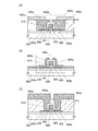
図1(A)及び(B)に示すトランジスタ440aは、トップゲート構造のトランジスタ
の一例である。図1(A)は平面図であり、図1(A)中の一点鎖線X1−Y1で切断し
た断面が図1(B)に相当する。なお図1(A)においては、層間絶縁膜415は省略し
ている。
A
チャネル長方向の断面図である図1(B)に示すように、トランジスタ440aを含む半
導体装置は、酸化物絶縁膜436が設けられた絶縁表面を有する基板400上に、チャネ
ル形成領域409、低抵抗領域404a、404bを含む酸化物半導体膜403、ゲート
絶縁膜402、ゲート電極層401、ゲート電極層401の上面及び側面を覆う酸化アル
ミニウム膜を含む絶縁膜414、層間絶縁膜415、ソース電極層405a、ドレイン電
極層405bを有する。
As shown in FIG. 1B, which is a cross-sectional view in the channel length direction, a semiconductor device including the
層間絶縁膜415はトランジスタ440aによる凹凸を平坦化するように設けられており
、低抵抗領域404a、404b、酸化アルミニウム膜を含む絶縁膜414、ゲート絶縁
膜402が露出する開口を有している。該開口に、酸化物半導体膜403の低抵抗領域4
04a、404b、ゲート絶縁膜402、並びに酸化アルミニウム膜を含む絶縁膜414
の上面及び側面の一部に接してソース電極層405a、及びドレイン電極層405bが設
けられている。
The
04a, 404b,
A
本実施の形態では、酸化アルミニウム膜を含む絶縁膜414として酸化アルミニウム膜を
用いる。酸化アルミニウム膜を高密度(膜密度3.2g/cm3以上、好ましくは3.6
g/cm3以上)とすることによって、トランジスタ440aに安定な電気的特性を付与
することができる。膜密度はラザフォード後方散乱法(RBS:Rutherford
Backscattering Spectrometry)や、X線反射率測定法(X
RR:X−Ray Reflection)によって測定することができる。また、酸化
アルミニウム膜は、膜中(バルク中)に少なくとも化学量論比を超える量の酸素が存在す
ることが好ましい。例えば、酸化アルミニウム膜を用いる場合には、AlOx(ただし、
x>1.5)とすればよい。
In this embodiment, an aluminum oxide film is used as the insulating
g / cm 3 or more), stable electrical characteristics can be imparted to the
Backscattering Spectrometry) and X-ray reflectivity measurement method (X
It can be measured by RR: X-Ray Reflection. In addition, it is preferable that the aluminum oxide film contains oxygen in an amount exceeding the stoichiometric ratio in the film (in the bulk). For example, when an aluminum oxide film is used, AlO x (however,
x> 1.5).
ゲート電極層401の上面及び側面が酸化アルミニウム膜を含む絶縁膜414で覆われて
いるため、ソース電極層405a及びドレイン電極層405bがゲート電極層401の上
面と重畳しても酸化アルミニウム膜を含む絶縁膜414によって、ソース電極層405a
又はドレイン電極層405bとゲート電極層401とのショート等の電気的不良を防止す
ることができる。よって、微細な構造を有するトランジスタ440aを歩留まりよく作製
することができる。
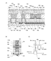
Since the upper surface and the side surface of the
Alternatively, an electrical failure such as a short circuit between the
酸化アルミニウム膜を含む絶縁膜は、ゲート電極層の上面及び側面を覆う構造であればよ
く、トランジスタ440aのようにゲート絶縁膜上に設けられてもよいし、酸化物半導体
膜と接する構造であってもよい。例えば、図3(A)に示すトランジスタ410aのよう
に、ゲート電極層401をマスクとしてゲート絶縁膜402をエッチングし、ゲート電極
層401及びゲート絶縁膜402の積層の上面及び側面を覆うように酸化アルミニウム膜
を含む絶縁膜414を設ける構造であってもよい。トランジスタ410aにおいては、酸
化物半導体膜403と酸化アルミニウム膜を含む絶縁膜414とが接する。
The insulating film including the aluminum oxide film may have a structure that covers the top surface and the side surface of the gate electrode layer, and may be provided over the gate insulating film like the
また、ゲート電極層の上面及び側面を覆う酸化アルミニウム膜を含む絶縁膜は、図3(A
)に示すように連続する単膜を用いることができる。また、複数の膜であってもよく、例
えば、図3(B)に示すトランジスタ410bのように、ゲート電極層401の側面を覆
う酸化アルミニウム膜を含む絶縁膜414a、414b、及びゲート電極層401の上面
を覆う酸化アルミニウム膜を含む絶縁膜414cの複数の膜を設ける構造であってもよい
。
In addition, an insulating film including an aluminum oxide film that covers the top surface and the side surface of the gate electrode layer is illustrated in FIG.
A continuous single film can be used as shown in FIG. Alternatively, a plurality of films may be used. For example, as in a
また、半導体装置の作製工程において、酸化物半導体膜403に、酸素(少なくとも、酸
素ラジカル、酸素原子、酸素イオン、のいずれかを含む)を導入して膜中に酸素を供給す
る。酸素の導入方法としては、イオン注入法、イオンドーピング法、プラズマイマージョ
ンイオンインプランテーション法、プラズマ処理などを用いることができる。
In the manufacturing process of the semiconductor device, oxygen (including at least one of oxygen radicals, oxygen atoms, and oxygen ions) is introduced into the
トランジスタ440aに設けられる酸化物半導体膜403は、酸化物半導体が結晶状態に
おける化学量論的組成に対し、酸素の含有量が過剰な領域が含まれている膜とすると好ま
しい。この場合、酸素の含有量は、酸化物半導体の化学量論比を超える程度とする。ある
いは、酸素の含有量は、単結晶の場合の酸素の量を超える程度とする。酸化物半導体の格
子間に酸素が存在する場合もある。
The
ゲート電極層401の上面及び側面を、酸化アルミニウム膜を含む絶縁膜414で覆うこ
とによって、ゲート電極層401と重畳する酸化物半導体膜403のチャネル形成領域4
09及び低抵抗領域404a、404bの一部を、酸化アルミニウム膜を含む絶縁膜41
4で覆う構成とすることができる。
The upper surface and the side surface of the
09 and part of the
It can be set as the structure covered with 4. FIG.
酸化アルミニウム膜を含む絶縁膜414は、水素、水分などの不純物、及び酸素の両方に
対して膜を通過させない遮断効果(ブロック効果)が高い。
The insulating
従って、酸化アルミニウム膜を含む絶縁膜は、作製工程中及び作製後において、変動要因
となる水素、水分などの不純物の酸化物半導体膜への混入、及び酸化物半導体を構成する
主成分材料である酸素の酸化物半導体膜からの放出を防止する保護膜として機能する。従
って、トランジスタ440aに安定した電気的特性を付与することができる。
Therefore, an insulating film including an aluminum oxide film is a main component material that includes impurities such as hydrogen and moisture, which cause fluctuations, in the oxide semiconductor film during and after the manufacturing process, and the oxide semiconductor. It functions as a protective film for preventing release of oxygen from the oxide semiconductor film. Accordingly, stable electrical characteristics can be imparted to the
なお、ゲート電極層401をマスクとして酸化物半導体膜403に自己整合的にドーパン
トを導入し、酸化物半導体膜403においてチャネル形成領域409を挟んでチャネル形
成領域409より抵抗が低く、ドーパントを含む低抵抗領域404a、404bを形成す
る。ドーパントは、酸化物半導体膜403の導電率を変化させる不純物である。ドーパン
トの導入方法としては、イオン注入法、イオンドーピング法、プラズマイマージョンイオ
ンインプランテーション法などを用いることができる。
Note that a dopant is introduced into the
チャネル長方向にチャネル形成領域409を挟んで低抵抗領域404a、404bを含む
酸化物半導体膜403を有することにより、該トランジスタ440aはオン特性(例えば
、オン電流及び電界効果移動度)が高く、高速動作、高速応答が可能となる。
By including the
酸化物半導体膜403に用いる酸化物半導体としては、少なくともインジウム(In)あ
るいは亜鉛(Zn)を含むことが好ましい。特にInとZnを含むことが好ましい。また
、該酸化物を用いたトランジスタの電気的特性のばらつきを減らすためのスタビライザー
として、それらに加えてガリウム(Ga)を有することが好ましい。また、スタビライザ
ーとしてスズ(Sn)を有することが好ましい。また、スタビライザーとしてハフニウム
(Hf)を有することが好ましい。また、スタビライザーとしてアルミニウム(Al)を
有することが好ましい。また、スタビライザーとしてジルコニウム(Zr)を有すること
が好ましい。
An oxide semiconductor used for the
また、他のスタビライザーとして、ランタノイドである、ランタン(La)、セリウム(
Ce)、プラセオジム(Pr)、ネオジム(Nd)、サマリウム(Sm)、ユウロピウム
(Eu)、ガドリニウム(Gd)、テルビウム(Tb)、ジスプロシウム(Dy)、ホル
ミウム(Ho)、エルビウム(Er)、ツリウム(Tm)、イッテルビウム(Yb)、ル
テチウム(Lu)のいずれか一種あるいは複数種を有してもよい。
In addition, as other stabilizers, lanthanoids such as lanthanum (La), cerium (
Ce), praseodymium (Pr), neodymium (Nd), samarium (Sm), europium (Eu), gadolinium (Gd), terbium (Tb), dysprosium (Dy), holmium (Ho), erbium (Er), thulium ( Tm), ytterbium (Yb), or lutetium (Lu) may be used alone or in combination.
例えば、酸化物半導体として、酸化インジウム、酸化スズ、酸化亜鉛、二元系金属の酸化
物であるIn−Zn系酸化物、Sn−Zn系酸化物、Al−Zn系酸化物、Zn−Mg系
酸化物、Sn−Mg系酸化物、In−Mg系酸化物、In−Ga系酸化物、三元系金属の
酸化物であるIn−Ga−Zn系酸化物(IGZOとも表記する)、In−Al−Zn系
酸化物、In−Sn−Zn系酸化物、Sn−Ga−Zn系酸化物、Al−Ga−Zn系酸
化物、Sn−Al−Zn系酸化物、In−Hf−Zn系酸化物、In−La−Zn系酸化
物、In−Ce−Zn系酸化物、In−Pr−Zn系酸化物、In−Nd−Zn系酸化物
、In−Sm−Zn系酸化物、In−Eu−Zn系酸化物、In−Gd−Zn系酸化物、
In−Tb−Zn系酸化物、In−Dy−Zn系酸化物、In−Ho−Zn系酸化物、I
n−Er−Zn系酸化物、In−Tm−Zn系酸化物、In−Yb−Zn系酸化物、In
−Lu−Zn系酸化物、四元系金属の酸化物であるIn−Sn−Ga−Zn系酸化物、I
n−Hf−Ga−Zn系酸化物、In−Al−Ga−Zn系酸化物、In−Sn−Al−
Zn系酸化物、In−Sn−Hf−Zn系酸化物、In−Hf−Al−Zn系酸化物を用
いることができる。
For example, as an oxide semiconductor, indium oxide, tin oxide, zinc oxide, binary metal oxides such as In—Zn oxide, Sn—Zn oxide, Al—Zn oxide, Zn—Mg oxide Oxides, Sn—Mg oxides, In—Mg oxides, In—Ga oxides, In—Ga—Zn oxides (also referred to as IGZO) which are oxides of ternary metals, In— Al-Zn oxide, In-Sn-Zn oxide, Sn-Ga-Zn oxide, Al-Ga-Zn oxide, Sn-Al-Zn oxide, In-Hf-Zn oxide In-La-Zn-based oxide, In-Ce-Zn-based oxide, In-Pr-Zn-based oxide, In-Nd-Zn-based oxide, In-Sm-Zn-based oxide, In-Eu -Zn-based oxide, In-Gd-Zn-based oxide,
In-Tb-Zn-based oxide, In-Dy-Zn-based oxide, In-Ho-Zn-based oxide, I
n-Er-Zn-based oxide, In-Tm-Zn-based oxide, In-Yb-Zn-based oxide, In
-Lu-Zn-based oxide, In-Sn-Ga-Zn-based oxide which is an oxide of a quaternary metal, I
n-Hf-Ga-Zn-based oxide, In-Al-Ga-Zn-based oxide, In-Sn-Al-
A Zn-based oxide, an In-Sn-Hf-Zn-based oxide, or an In-Hf-Al-Zn-based oxide can be used.
なお、ここで、例えば、In−Ga−Zn系酸化物とは、InとGaとZnを主成分とし
て有する酸化物という意味であり、InとGaとZnの比率は問わない。また、InとG
aとZn以外の金属元素が入っていてもよい。
Note that here, for example, an In—Ga—Zn-based oxide means an oxide containing In, Ga, and Zn as its main components, and there is no limitation on the ratio of In, Ga, and Zn. In and G
Metal elements other than a and Zn may be contained.
また、酸化物半導体として、InMO3(ZnO)m(m>0、且つ、mは整数でない)
で表記される材料を用いてもよい。なお、Mは、Ga、Fe、Mn及びCoから選ばれた
一の金属元素または複数の金属元素を示す。また、酸化物半導体として、In2SnO5
(ZnO)n(n>0、且つ、nは整数)で表記される材料を用いてもよい。
In addition, as an oxide semiconductor, InMO 3 (ZnO) m (m> 0 and m is not an integer)
A material represented by may be used. Note that M represents one metal element or a plurality of metal elements selected from Ga, Fe, Mn, and Co. As an oxide semiconductor, In 2 SnO 5
A material represented by (ZnO) n (n> 0 and n is an integer) may be used.
例えば、In:Ga:Zn=1:1:1(=1/3:1/3:1/3)、In:Ga:Z
n=2:2:1(=2/5:2/5:1/5)、あるいはIn:Ga:Zn=3:1:2
(=1/2:1/6:1/3)の原子数比のIn−Ga−Zn系酸化物やその組成の近傍
の酸化物を用いることができる。あるいは、In:Sn:Zn=1:1:1(=1/3:
1/3:1/3)、In:Sn:Zn=2:1:3(=1/3:1/6:1/2)あるい
はIn:Sn:Zn=2:1:5(=1/4:1/8:5/8)の原子数比のIn−Sn
−Zn系酸化物やその組成の近傍の酸化物を用いるとよい。
For example, In: Ga: Zn = 1: 1: 1 (= 1/3: 1/3: 1/3), In: Ga: Z
n = 2: 2: 1 (= 2/5: 2/5: 1/5), or In: Ga: Zn = 3: 1: 2
An In—Ga—Zn-based oxide having an atomic ratio of (= 1/2: 1/6: 1/3) or an oxide in the vicinity of the composition thereof can be used. Alternatively, In: Sn: Zn = 1: 1: 1 (= 1/3:
1/3: 1/3), In: Sn: Zn = 2: 1: 3 (= 1/3: 1/6: 1/2) or In: Sn: Zn = 2: 1: 5 (= 1 / 4: 1/8: 5/8) atomic ratio In-Sn
A Zn-based oxide or an oxide in the vicinity of the composition may be used.
しかし、これらに限られず、必要とする半導体特性(移動度、しきい値、ばらつき等)に
応じて適切な組成のものを用いればよい。また、必要とする半導体特性を得るために、キ
ャリア濃度や不純物濃度、欠陥密度、金属元素と酸素の原子数比、原子間距離、密度等を
適切なものとすることが好ましい。
However, the composition is not limited thereto, and a material having an appropriate composition may be used depending on required semiconductor characteristics (mobility, threshold value, variation, etc.). In order to obtain the required semiconductor characteristics, it is preferable that the carrier concentration, the impurity concentration, the defect density, the atomic ratio between the metal element and oxygen, the interatomic distance, the density, and the like are appropriate.
例えば、In−Sn−Zn系酸化物では比較的容易に高い移動度が得られる。しかしなが
ら、In−Ga−Zn系酸化物でも、バルク内欠陥密度を低くすることにより移動度を上
げることができる。
For example, high mobility can be obtained relatively easily with an In—Sn—Zn-based oxide. However, mobility can be increased by reducing the defect density in the bulk also in the case of using an In—Ga—Zn-based oxide.
なお、例えば、In、Ga、Znの原子数比がIn:Ga:Zn=a:b:c(a+b+
c=1)である酸化物の組成が、原子数比がIn:Ga:Zn=A:B:C(A+B+C
=1)の酸化物の組成の近傍であるとは、a、b、cが、(a−A)2+(b−B)2+
(c−C)2≦r2を満たすことをいう。rとしては、例えば、0.05とすればよい。
他の酸化物でも同様である。
For example, the atomic ratio of In, Ga, and Zn is In: Ga: Zn = a: b: c (a + b +
The composition of the oxide having c = 1) has an atomic ratio of In: Ga: Zn = A: B: C (A + B + C).
= 1) In the vicinity of the oxide composition, a, b, and c are (a−A) 2 + (b−B) 2 +
(C−C) 2 ≦ r 2 is satisfied. For example, r may be 0.05.
The same applies to other oxides.
酸化物半導体膜403は、単結晶、多結晶(ポリクリスタルともいう。)または非晶質な
どの状態をとる。
The
好ましくは、酸化物半導体膜は、CAAC−OS(C Axis Aligned Cr
ystalline Oxide Semiconductor)膜とする。
Preferably, the oxide semiconductor film is a CAAC-OS (C Axis Aligned Cr).
(ystalline Oxide Semiconductor) film.
CAAC−OS膜は、完全な単結晶ではなく、完全な非晶質でもない。CAAC−OS膜
は、非晶質相に結晶部を有する結晶−非晶質混相構造の酸化物半導体膜である。なお、当
該結晶部は、一辺が100nm未満の立方体内に収まる大きさであることが多い。また、
透過型電子顕微鏡(TEM:Transmission Electron Micro
scope)による観察像では、CAAC−OS膜に含まれる非晶質部と結晶部との境界
は明確ではない。また、TEMによってCAAC−OS膜には粒界(グレインバウンダリ
ーともいう。)は確認できない。そのため、CAAC−OS膜は、粒界に起因する電子移
動度の低下が抑制される。
The CAAC-OS film is not completely single crystal nor completely amorphous. The CAAC-OS film is an oxide semiconductor film with a crystal-amorphous mixed phase structure where crystal parts are included in an amorphous phase. Note that the crystal part is often large enough to fit in a cube whose one side is less than 100 nm. Also,
Transmission Electron Microscope (TEM: Transmission Electron Micro)
In the observation image by (scope), the boundary between the amorphous part and the crystal part included in the CAAC-OS film is not clear. Further, a grain boundary (also referred to as a grain boundary) cannot be confirmed in the CAAC-OS film by TEM. Therefore, in the CAAC-OS film, reduction in electron mobility due to grain boundaries is suppressed.
CAAC−OS膜に含まれる結晶部は、c軸がCAAC−OS膜の被形成面の法線ベクト
ルまたは表面の法線ベクトルに平行な方向に揃い、かつab面に垂直な方向から見て三角
形状または六角形状の原子配列を有し、c軸に垂直な方向から見て金属原子が層状または
金属原子と酸素原子とが層状に配列している。なお、異なる結晶部間で、それぞれa軸お
よびb軸の向きが異なっていてもよい。本明細書において、単に垂直と記載する場合、8
5°以上95°以下の範囲も含まれることとする。また、単に平行と記載する場合、−5
°以上5°以下の範囲も含まれることとする。
In the crystal part included in the CAAC-OS film, the c-axis is aligned in a direction parallel to the normal vector of the formation surface of the CAAC-OS film or the normal vector of the surface, and triangular when viewed from the direction perpendicular to the ab plane. It has a shape or hexagonal atomic arrangement, and metal atoms are arranged in layers or metal atoms and oxygen atoms are arranged in layers as viewed from the direction perpendicular to the c-axis. Note that the directions of the a-axis and the b-axis may be different between different crystal parts. In the present specification, when simply described as vertical, 8
The range of 5 ° to 95 ° is also included. In addition, when simply described as parallel, −5
A range of not less than 5 ° and not more than 5 ° is also included.
なお、CAAC−OS膜において、結晶部の分布が一様でなくてもよい。例えば、CAA
C−OS膜の形成過程において、酸化物半導体膜の表面側から結晶成長させる場合、被形
成面の近傍に対し表面の近傍では結晶部の占める割合が高くなることがある。また、CA
AC−OS膜へ不純物を添加することにより、当該不純物添加領域において結晶部が非晶
質化することもある。
Note that the distribution of crystal parts in the CAAC-OS film is not necessarily uniform. For example, CAA
In the formation process of the C-OS film, when crystal growth is performed from the surface side of the oxide semiconductor film, the ratio of crystal parts in the vicinity of the surface of the oxide semiconductor film may be higher in the vicinity of the surface. CA
When an impurity is added to the AC-OS film, the crystal part in a region to which the impurity is added becomes amorphous in some cases.
CAAC−OS膜に含まれる結晶部のc軸は、CAAC−OS膜の被形成面の法線ベクト
ルまたは表面の法線ベクトルに平行な方向に揃うため、CAAC−OS膜の形状(被形成
面の断面形状または表面の断面形状)によっては互いに異なる方向を向くことがある。な
お、結晶部のc軸の方向は、CAAC−OS膜が形成されたときの被形成面の法線ベクト
ルまたは表面の法線ベクトルに平行な方向となる。結晶部は、成膜することにより、また
は成膜後に加熱処理などの結晶化処理を行うことにより形成される。
Since the c-axis of the crystal part included in the CAAC-OS film is aligned in a direction parallel to the normal vector of the formation surface of the CAAC-OS film or the normal vector of the surface, the shape of the CAAC-OS film (formation surface) Depending on the cross-sectional shape of the surface or the cross-sectional shape of the surface). Note that the c-axis direction of the crystal part is parallel to the normal vector of the surface where the CAAC-OS film is formed or the normal vector of the surface. The crystal part is formed by film formation or by performing crystallization treatment such as heat treatment after film formation.
CAAC−OS膜を用いたトランジスタは、可視光や紫外光の照射による電気的特性の変
動を低減することが可能である。よって、当該トランジスタは、信頼性が高い。
A transistor including a CAAC-OS film can reduce variation in electrical characteristics due to irradiation with visible light or ultraviolet light. Therefore, the transistor has high reliability.
なお、酸化物半導体膜を構成する酸素の一部は窒素で置換されてもよい。 Note that part of oxygen included in the oxide semiconductor film may be replaced with nitrogen.
また、CAAC−OSのように結晶部を有する酸化物半導体では、よりバルク内欠陥を低
減することができ、表面の平坦性を高めればアモルファス状態の酸化物半導体以上の移動
度を得ることができる。表面の平坦性を高めるためには、平坦な表面上に酸化物半導体を
形成することが好ましく、具体的には、平均面粗さ(Ra)が1nm以下、好ましくは0
.3nm以下、より好ましくは0.1nm以下の表面上に形成するとよい。
Further, in an oxide semiconductor having a crystal part such as a CAAC-OS, defects in a bulk can be further reduced, and mobility higher than that of an oxide semiconductor in an amorphous state can be obtained by increasing surface flatness. . In order to improve the flatness of the surface, it is preferable to form an oxide semiconductor on the flat surface. Specifically, the average surface roughness (Ra) is 1 nm or less, preferably 0.
. It may be formed on the surface of 3 nm or less, more preferably 0.1 nm or less.
Raとは、JIS B 0601:2001(ISO4287:1997)で定義されて
いる算術平均粗さを曲面に対して適用できるよう三次元に拡張したものであり、「基準面
から指定面までの偏差の絶対値を平均した値」で表現でき、以下の式にて定義される。
Ra is an arithmetic mean roughness defined in JIS B 0601: 2001 (ISO4287: 1997) extended to three dimensions so that it can be applied to curved surfaces. It can be expressed as “average value of absolute values” and is defined by the following equation.
![]()
![]()
ここで、指定面とは、粗さ計測の対象となる面であり、座標(x1,y1,f(x1,y
1)),(x1,y2,f(x1,y2)),(x2,y1,f(x2,y1)),(x
2,y2,f(x2,y2))の4点で表される四角形の領域とし、指定面をxy平面に
投影した長方形の面積をS0、基準面の高さ(指定面の平均の高さ)をZ0とする。Ra
は原子間力顕微鏡(AFM:Atomic Force Microscope)にて測
定可能である。
Here, the designated surface is a surface to be subjected to roughness measurement, and the coordinates (x 1 , y 1 , f (x 1 , y
1)), (x 1, y 2, f (x 1, y 2)), (x 2, y 1, f (x 2, y 1)), (x
2 , y 2 , f (x 2 , y 2 )), a rectangular region represented by four points, and the rectangular area obtained by projecting the designated surface onto the xy plane is S 0 , and the height of the reference surface (of the designated surface) Let Z 0 be the average height. Ra
Can be measured with an atomic force microscope (AFM).
酸化物半導体膜403の膜厚は、1nm以上30nm以下(好ましくは5nm以上10n
m以下)とし、スパッタリング法、MBE(Molecular Beam Epita
xy)法、CVD法、パルスレーザ堆積法、ALD(Atomic Layer Dep
osition)法等を適宜用いることができる。また、酸化物半導体膜403は、スパ
ッタリングターゲット表面に対し、概略垂直に複数の基板表面がセットされた状態で成膜
を行うスパッタ装置を用いて成膜してもよい。
The thickness of the
m or less), sputtering method, MBE (Molecular Beam Epita)
xy) method, CVD method, pulsed laser deposition method, ALD (Atomic Layer Dep)
osition) method or the like can be used as appropriate. Alternatively, the
CAAC−OS膜は、例えば、多結晶である酸化物半導体スパッタリング用ターゲットを
用い、スパッタリング法によって成膜する。当該スパッタリング用ターゲットにイオンが
衝突すると、スパッタリング用ターゲットに含まれる結晶領域がa−b面から劈開し、a
−b面に平行な面を有する平板状またはペレット状のスパッタリング粒子として剥離する
ことがある。この場合、当該平板状のスパッタリング粒子が、結晶状態を維持したまま基
板に到達することで、CAAC−OS膜を成膜することができる。
For example, the CAAC-OS film is formed by a sputtering method using a polycrystalline oxide semiconductor sputtering target. When ions collide with the sputtering target, the crystal region included in the sputtering target is cleaved from the ab plane, and a
It may peel off as flat or pellet-like sputtered particles having a plane parallel to the -b plane. In this case, the flat-plate-like sputtered particle reaches the substrate while maintaining a crystalline state, whereby a CAAC-OS film can be formed.
また、CAAC−OS膜を成膜するために、以下の条件を適用することが好ましい。 In order to form the CAAC-OS film, the following conditions are preferably applied.
成膜時の不純物混入を低減することで、不純物によって結晶状態が崩れることを抑制でき
る。例えば、成膜室内に存在する不純物濃度(水素、水、二酸化炭素および窒素など)を
低減すればよい。また、成膜ガス中の不純物濃度を低減すればよい。具体的には、露点が
−80℃以下、好ましくは−100℃以下である成膜ガスを用いる。
By reducing the mixing of impurities during film formation, the crystal state can be prevented from being broken by impurities. For example, the concentration of impurities (such as hydrogen, water, carbon dioxide, and nitrogen) existing in the deposition chamber may be reduced. Further, the impurity concentration in the deposition gas may be reduced. Specifically, a deposition gas having a dew point of −80 ° C. or lower, preferably −100 ° C. or lower is used.
また、成膜時の基板加熱温度を高めることで、基板到達後にスパッタリング粒子のマイグ
レーションが起こる。具体的には、基板加熱温度を100℃以上740℃以下、好ましく
は200℃以上500℃以下として成膜する。成膜時の基板加熱温度を高めることで、平
板状のスパッタリング粒子が基板に到達した場合、基板上でマイグレーションが起こり、
スパッタリング粒子の平らな面が基板に付着する。
Further, by increasing the substrate heating temperature during film formation, migration of sputtered particles occurs after reaching the substrate. Specifically, the film is formed at a substrate heating temperature of 100 ° C. to 740 ° C., preferably 200 ° C. to 500 ° C. By increasing the substrate heating temperature during film formation, when flat sputtered particles reach the substrate, migration occurs on the substrate,
The flat surface of the sputtered particles adheres to the substrate.
また、成膜ガス中の酸素割合を高め、電力を最適化することで成膜時のプラズマダメージ
を軽減すると好ましい。成膜ガス中の酸素割合は、30体積%以上、好ましくは100体
積%とする。
In addition, it is preferable to reduce plasma damage during film formation by increasing the oxygen ratio in the film formation gas and optimizing electric power. The oxygen ratio in the deposition gas is 30% by volume or more, preferably 100% by volume.
スパッタリング用ターゲットの一例として、In−Ga−Zn−O化合物ターゲットにつ
いて以下に示す。
As an example of the sputtering target, an In—Ga—Zn—O compound target is described below.
InOX粉末、GaOY粉末およびZnOZ粉末を所定のmol数で混合し、加圧処理後
、1000℃以上1500℃以下の温度で加熱処理をすることで多結晶であるIn−Ga
−Zn−O化合物ターゲットとする。なお、X、YおよびZは任意の正数である。ここで
、所定のmol数比は、例えば、InOX粉末、GaOY粉末およびZnOZ粉末が、2
:2:1、8:4:3、3:1:1、1:1:1、4:2:3または3:1:2である。
なお、粉末の種類、およびその混合するmol数比は、作製するスパッタリング用ターゲ
ットによって適宜変更すればよい。
In-Ga that is polycrystalline by mixing InO X powder, GaO Y powder, and ZnO Z powder in a predetermined number of moles, and after heat treatment at a temperature of 1000 ° C. or higher and 1500 ° C. or lower.
—Zn—O compound target. X, Y and Z are arbitrary positive numbers. Here, the predetermined mole number ratio is, for example, 2 for InO X powder, GaO Y powder, and ZnO Z powder.
: 2: 1, 8: 4: 3, 3: 1: 1, 1: 1: 1, 4: 2: 3 or 3: 1: 2.
Note that the type of powder and the mol number ratio to be mixed may be changed as appropriate depending on the sputtering target to be manufactured.
図2(A)乃至(D)にトランジスタ440aを有する半導体装置の作製方法の一例を示
す。
2A to 2D illustrate an example of a method for manufacturing a semiconductor device including the
まず、絶縁表面を有する基板400上に酸化物絶縁膜436を形成する。
First, the
絶縁表面を有する基板400に使用することができる基板に大きな制限はないが、少なく
とも、後の熱処理に耐えうる程度の耐熱性を有していることが必要となる。例えば、バリ
ウムホウケイ酸ガラスやアルミノホウケイ酸ガラスなどのガラス基板、セラミック基板、
石英基板、サファイア基板などを用いることができる。また、シリコンや炭化シリコンな
どの単結晶半導体基板、多結晶半導体基板、シリコンゲルマニウムなどの化合物半導体基
板、SOI基板などを適用することもでき、これらの基板上に半導体素子が設けられたも
のを、基板400として用いてもよい。
There is no particular limitation on a substrate that can be used as the
A quartz substrate, a sapphire substrate, or the like can be used. In addition, a single crystal semiconductor substrate such as silicon or silicon carbide, a polycrystalline semiconductor substrate, a compound semiconductor substrate such as silicon germanium, an SOI substrate, or the like can be applied, and a semiconductor element provided on these substrates, The
また、基板400として、可撓性基板を用いて半導体装置を作製してもよい。可撓性を有
する半導体装置を作製するには、可撓性基板上に酸化物半導体膜403を含むトランジス
タ440aを直接作製してもよいし、他の作製基板に酸化物半導体膜403を含むトラン
ジスタ440aを作製し、その後可撓性基板に剥離、転置してもよい。なお、作製基板か
ら可撓性基板に剥離、転置するために、作製基板と酸化物半導体膜を含むトランジスタ4
40aとの間に剥離層を設けるとよい。
Alternatively, a semiconductor device may be manufactured using a flexible substrate as the
It is preferable to provide a release layer between 40a.
酸化物絶縁膜436としては、プラズマCVD法又はスパッタリング法等により、酸化シ
リコン、酸化窒化シリコン、酸化アルミニウム、酸化窒化アルミニウム、酸化ハフニウム
、酸化ガリウム、又はこれらの混合材料を用いて形成することができる。
The
酸化物絶縁膜436は、単層でも積層でもよい。例えば、基板400上に酸化シリコン膜
、In−Hf−Zn系酸化物膜、酸化物半導体膜403を順に積層してもよいし、基板4
00上に酸化シリコン膜、In:Zr:Zn=1:1:1の原子数比のIn−Zr−Zn
系酸化物膜、酸化物半導体膜403を順に積層してもよいし、基板400上に酸化シリコ
ン膜、In:Gd:Zn=1:1:1の原子数比のIn−Gd−Zn系酸化物膜、酸化物
半導体膜403を順に積層してもよい。
The
A silicon oxide film on 00, In: Zr: Zn = 1: 1: 1 atomic ratio In—Zr—Zn
A base oxide film and an
本実施の形態では酸化物絶縁膜436としてスパッタリング法を用いて形成する酸化シリ
コン膜を用いる。
In this embodiment, a silicon oxide film formed by a sputtering method is used as the
また、酸化物絶縁膜436と基板400との間に窒化物絶縁膜を設けてもよい。窒化物絶
縁膜は、プラズマCVD法又はスパッタリング法等により、窒化シリコン、窒化酸化シリ
コン、窒化アルミニウム、窒化酸化アルミニウム、又はこれらの混合材料を用いて形成す
ることができる。
Further, a nitride insulating film may be provided between the
次に、酸化物絶縁膜436上に酸化物半導体膜403を形成する。
Next, the
酸化物絶縁膜436は、酸化物半導体膜403と接するため、膜中(バルク中)に少なく
とも化学量論比を超える量の酸素が存在することが好ましい。例えば、酸化物絶縁膜43
6として、酸化シリコン膜を用いる場合には、SiO2+α(ただし、α>0)とする。
このような酸化物絶縁膜436を用いることで、酸化物半導体膜403に酸素を供給する
ことができ、特性を良好にすることができる。酸化物半導体膜403へ酸素を供給するこ
とにより、膜中の酸素欠損を補填することができる。
Since the
6, when a silicon oxide film is used, SiO 2 + α (where α> 0).
By using such an
例えば、酸素の供給源となる酸素を多く(過剰に)含む酸化物絶縁膜436を酸化物半導
体膜403と接して設けることによって、該酸化物絶縁膜436から酸化物半導体膜40
3へ酸素を供給することができる。酸化物半導体膜403及び酸化物絶縁膜436を少な
くとも一部が接した状態で加熱処理を行うことによって酸化物半導体膜403への酸素の
供給を行ってもよい。
For example, by providing the
3 can be supplied with oxygen. Oxygen may be supplied to the
酸化物半導体膜403の形成工程において、酸化物半導体膜403に水素、又は水がなる
べく含まれないようにするために、酸化物半導体膜403の成膜の前処理として、スパッ
タリング装置の予備加熱室で酸化物絶縁膜436が形成された基板を予備加熱し、基板及
び酸化物絶縁膜436に吸着した水素、水分などの不純物を脱離し排気することが好まし
い。なお、予備加熱室に設ける排気手段はクライオポンプが好ましい。
In the formation process of the
酸化物絶縁膜436において酸化物半導体膜403が接して形成される領域に、平坦化処
理を行ってもよい。平坦化処理としては、特に限定されないが、研磨処理(例えば、化学
的機械研磨法)、ドライエッチング処理、プラズマ処理を用いることができる。
Planarization treatment may be performed on a region where the
プラズマ処理としては、例えば、アルゴンガスを導入してプラズマを発生させる逆スパッ
タリングを行うことができる。逆スパッタリングとは、アルゴン雰囲気下で基板側にRF
電源を用いて電圧を印加して基板近傍にプラズマを形成して表面を改質する方法である。
なお、アルゴン雰囲気に代えて窒素、ヘリウム、酸素などを用いてもよい。逆スパッタリ
ングを行うと、酸化物絶縁膜436の表面に付着している粉状物質(パーティクル、ごみ
ともいう)を除去することができる。
As the plasma treatment, for example, reverse sputtering in which an argon gas is introduced to generate plasma can be performed. Reverse sputtering is RF on the substrate side in an argon atmosphere.
In this method, a voltage is applied using a power source to form plasma in the vicinity of the substrate to modify the surface.
Note that nitrogen, helium, oxygen, or the like may be used instead of the argon atmosphere. By performing reverse sputtering, powdery substances (also referred to as particles or dust) attached to the surface of the
平坦化処理として、研磨処理、ドライエッチング処理、プラズマ処理は複数回行ってもよ
く、それらを組み合わせて行ってもよい。また、組み合わせて行う場合、工程順も特に限
定されず、酸化物絶縁膜436表面の凹凸状態に合わせて適宜設定すればよい。
As the planarization treatment, the polishing treatment, the dry etching treatment, and the plasma treatment may be performed a plurality of times or in combination. In the case where the steps are performed in combination, the order of steps is not particularly limited, and may be set as appropriate depending on the unevenness state of the surface of the
平坦化処理は、例えば、酸化物絶縁膜436として用いる酸化シリコン膜表面に化学的機
械研磨法により研磨処理を行い、酸化シリコン膜表面における平均面粗さ(Ra)を約0
.15nmとすればよい。
In the planarization treatment, for example, the surface of the silicon oxide film used as the
. What is necessary is just to be 15 nm.
なお、酸化物半導体膜403は、成膜時に酸素が多く含まれるような条件(例えば、酸素
100%の雰囲気下でスパッタリング法により成膜を行うなど)で成膜して、酸素を多く
含む(好ましくは酸化物半導体が結晶状態における化学量論的組成に対し、酸素の含有量
が過剰な領域が含まれている)膜とすることが好ましい。
Note that the
なお、本実施の形態において、酸化物半導体膜403を、スパッタリング法で作製するた
めのターゲットとしては、組成として、In:Ga:Zn=3:1:2[原子数比]の金
属酸化物ターゲットを用い、In−Ga−Zn系酸化物膜(IGZO膜)を成膜する。
Note that in this embodiment, as a target for forming the
また、金属酸化物ターゲットの相対密度(充填率)は90%以上100%以下、好ましく
は95%以上99.9%以下である。相対密度の高い金属酸化物ターゲットを用いること
により、成膜した酸化物半導体膜は緻密な膜とすることができる。
The relative density (filling rate) of the metal oxide target is 90% to 100%, preferably 95% to 99.9%. By using a metal oxide target having a high relative density, the formed oxide semiconductor film can be a dense film.
酸化物半導体膜403を、成膜する際に用いるスパッタリングガスは水素、水、水酸基又
は水素化物などの不純物が除去された高純度ガスを用いることが好ましい。
As a sputtering gas used for forming the
減圧状態に保持された成膜室内に基板を保持する。そして、成膜室内の残留水分を除去し
つつ水素及び水分が除去されたスパッタガスを導入し、上記ターゲットを用いて基板40
0上に酸化物半導体膜403を成膜する。成膜室内の残留水分を除去するためには、吸着
型の真空ポンプ、例えば、クライオポンプ、イオンポンプ、チタンサブリメーションポン
プを用いることが好ましい。また、排気手段としては、ターボ分子ポンプにコールドトラ
ップを加えたものであってもよい。クライオポンプを用いて排気した成膜室は、例えば、
水素原子、水(H2O)など水素原子を含む化合物(より好ましくは炭素原子を含む化合
物も)等が排気されるため、当該成膜室で成膜した酸化物半導体膜403に含まれる不純
物の濃度を低減できる。
The substrate is held in a film formation chamber held in a reduced pressure state. Then, a sputtering gas from which hydrogen and moisture have been removed is introduced while moisture remaining in the film formation chamber is removed, and the substrate 40 is used using the target.
An
Since a compound containing a hydrogen atom such as a hydrogen atom or water (H 2 O) (more preferably a compound containing a carbon atom) is exhausted, an impurity contained in the
また、酸化物絶縁膜436と酸化物半導体膜403とを大気に解放せずに連続的に形成す
ることが好ましい。酸化物絶縁膜436と酸化物半導体膜403とを大気に曝露せずに連
続して形成すると、酸化物絶縁膜436表面に水素や水分などの不純物が吸着することを
防止することができる。
The
次に、酸化物半導体膜403に酸素(少なくとも、酸素ラジカル、酸素原子、酸素イオン
、のいずれかを含む)を導入して、酸化物半導体膜に酸素の供給を行う。酸素の導入方法
としては、イオン注入法、イオンドーピング法、プラズマイマージョンイオンインプラン
テーション法、プラズマ処理などを用いることができる。
Next, oxygen (including at least one of oxygen radicals, oxygen atoms, and oxygen ions) is introduced into the
本実施の形態におけるトランジスタ440aの作製工程において、酸素の導入工程は、酸
化物半導体膜403の形成後、ゲート電極層401が形成される前までに行うことが好ま
しい。酸化物半導体膜403への酸素の導入は複数回行ってもよい。
In the manufacturing process of the
また、酸素の導入工程は、酸化物半導体膜403に直接導入してもよいし、ゲート絶縁膜
などの他の膜を通過して酸化物半導体膜403へ導入してもよい。酸素を酸化物半導体膜
403に他の膜を通過して導入する場合は、イオン注入法、イオンドーピング法、プラズ
マイマージョンイオンインプランテーション法などを用いればよいが、酸素を露出された
酸化物半導体膜403へ直接導入する場合は、プラズマ処理なども用いることができる。
The oxygen introduction step may be directly introduced into the
本実施の形態では、イオン注入法により酸化物半導体膜403に酸素を注入する。酸素の
注入工程により、酸化物半導体膜403は、酸化物半導体が結晶状態における化学量論的
組成に対し、酸素の含有量が過剰な領域が含まれている酸化物半導体膜403となる。
In this embodiment, oxygen is implanted into the
例えば、酸素の導入工程によって導入された酸化物半導体膜403における酸素濃度を1
×1018/cm3以上3×1021/cm3以下とするのが好ましい。なお、酸素過剰
領域は、酸化物半導体膜403の一部(界面も含む)に存在していればよい。よって、酸
素を導入することにより、酸化物絶縁膜436、酸化物半導体膜403、及びゲート絶縁
膜402の積層において、酸化物絶縁膜436と酸化物半導体膜403との界面、酸化物
半導体膜403中、又は酸化物半導体膜403とゲート絶縁膜402との界面の少なくと
も一に酸素を含有させる。
For example, the oxygen concentration in the
× preferably set to 10 18 / cm 3 or more 3 × 10 21 / cm 3 or less. Note that the oxygen excess region only needs to exist in part (including the interface) of the
酸化物半導体膜403は、酸化物半導体が結晶状態における化学量論的組成に対し、酸素
の含有量が過剰な領域が含まれている。この場合、酸素の含有量は、酸化物半導体の化学
量論比を超える程度とする。あるいは、酸素の含有量は、単結晶の場合の酸素の量を超え
る程度とする。酸化物半導体の格子間に酸素が存在する場合もある。このような酸化物半
導体の組成はInGaZnmOm+3x(x>1)で表すことができる。例えば、m=1
であるとき、酸化物半導体の組成はInGaZnO1+3x(x>1)となり、酸素過剰
である場合には、1+3xが4を越える値を示す。
The
In this case, the composition of the oxide semiconductor is InGaZnO 1 + 3x (x> 1). When oxygen is excessive, 1 + 3x exceeds 4.
供給された酸素によって、酸化物半導体膜403中に存在する酸素欠損を補填することが
できる。
With the supplied oxygen, oxygen vacancies existing in the
なお、酸化物半導体において、酸素は主たる成分材料の一つである。このため、酸化物半
導体膜中の酸素濃度を、SIMS(Secondary Ion Mass Spect
rometry)などの方法を用いて、正確に見積もることは難しい。つまり、酸化物半
導体膜に酸素が意図的に添加されたか否かを判別することは困難であるといえる。
Note that oxygen is one of main component materials in an oxide semiconductor. Therefore, the oxygen concentration in the oxide semiconductor film is changed to SIMS (Secondary Ion Mass Spec.
It is difficult to estimate accurately using a method such as (rometry). That is, it can be said that it is difficult to determine whether oxygen is intentionally added to the oxide semiconductor film.
ところで、酸素には17Oや18Oといった同位体が存在し、自然界におけるこれらの存
在比率はそれぞれ酸素原子全体の0.037%、0.204%程度であることが知られて
いる。つまり、酸化物半導体膜中におけるこれら同位体の濃度は、SIMSなどの方法に
よって見積もることができる程度になるから、これらの濃度を測定することで、酸化物半
導体膜中の酸素濃度をより正確に見積もることが可能な場合がある。よって、これらの濃
度を測定することで、酸化物半導体膜に意図的に酸素が添加されたか否かを判別してもよ
い。
By the way, it is known that oxygen has isotopes such as 17 O and 18 O, and their abundance ratios in the natural world are about 0.037% and 0.204% of the whole oxygen atom, respectively. In other words, since the concentration of these isotopes in the oxide semiconductor film can be estimated by a method such as SIMS, the oxygen concentration in the oxide semiconductor film can be more accurately measured by measuring these concentrations. It may be possible to estimate. Therefore, it may be determined whether oxygen is intentionally added to the oxide semiconductor film by measuring these concentrations.
本実施の形態のように、酸素を直接酸化物半導体膜403へ導入する場合は、酸化物半導
体膜403と接する絶縁膜(酸化物絶縁膜436、ゲート絶縁膜402など)を、必ずし
も酸素を多く含む膜とする必要はないが、酸化物半導体膜403と接する絶縁膜(酸化物
絶縁膜436、ゲート絶縁膜402など)を、酸素を多く含む膜とし、さらに酸素を直接
酸化物半導体膜403に導入し、複数の酸素供給方法を行ってもよい。
In the case where oxygen is introduced directly into the
次に、膜状の酸化物半導体膜403をフォトリソグラフィ工程により島状の酸化物半導体
膜403に加工する。
Next, the film-shaped
また、島状の酸化物半導体膜403を形成するためのレジストマスクをインクジェット法
で形成してもよい。レジストマスクをインクジェット法で形成するとフォトマスクを使用
しないため、製造コストを低減できる。
Further, a resist mask for forming the island-shaped
なお、酸化物半導体膜403のエッチングは、ドライエッチングでもウェットエッチング
でもよく、両方を用いてもよい。例えば、酸化物半導体膜403のウェットエッチングに
用いるエッチング液としては、燐酸と酢酸と硝酸を混ぜた溶液などを用いることができる
。また、ITO−07N(関東化学社製)を用いてもよい。また、ICP(Induct
ively Coupled Plasma:誘導結合型プラズマ)エッチング法による
ドライエッチングによってエッチング加工してもよい。例えば、IGZO膜をICPエッ
チング法により、エッチング(エッチング条件:エッチングガス(BCl3:Cl2=6
0sccm:20sccm)、電源電力450W、バイアス電力100W、圧力1.9P
a)し、島状に加工することができる。
Note that the etching of the
An etching process may be performed by dry etching by an ivory coupled plasma (inductively coupled plasma) etching method. For example, the IGZO film is etched by ICP etching (etching condition: etching gas (BCl 3 : Cl 2 = 6
0 sccm: 20 sccm), power source power 450 W, bias power 100 W, pressure 1.9 P
a) and can be processed into islands.
また、酸化物半導体膜403に、過剰な水素(水や水酸基を含む)を除去(脱水化または
脱水素化)するための加熱処理を行ってもよい。加熱処理の温度は、300℃以上700
℃以下、または基板の歪み点未満とする。加熱処理は減圧下又は窒素雰囲気下などで行う
ことができる。例えば、加熱処理装置の一つである電気炉に基板を導入し、酸化物半導体
膜403に対して窒素雰囲気下450℃において1時間の加熱処理を行う。
The
C. or less, or less than the strain point of the substrate. The heat treatment can be performed under reduced pressure or a nitrogen atmosphere. For example, a substrate is introduced into an electric furnace which is one of heat treatment apparatuses, and the
なお、加熱処理装置は電気炉に限られず、抵抗発熱体などの発熱体からの熱伝導または熱
輻射によって、被処理物を加熱する装置を用いてもよい。例えば、GRTA(Gas R
apid Thermal Anneal)装置、LRTA(Lamp Rapid T
hermal Anneal)装置等のRTA(Rapid Thermal Anne
al)装置を用いることができる。LRTA装置は、ハロゲンランプ、メタルハライドラ
ンプ、キセノンアークランプ、カーボンアークランプ、高圧ナトリウムランプ、高圧水銀
ランプなどのランプから発する光(電磁波)の輻射により、被処理物を加熱する装置であ
る。GRTA装置は、高温のガスを用いて加熱処理を行う装置である。高温のガスには、
アルゴンなどの希ガス、または窒素のような、加熱処理によって被処理物と反応しない不
活性気体が用いられる。
Note that the heat treatment apparatus is not limited to an electric furnace, and an apparatus for heating an object to be processed by heat conduction or heat radiation from a heating element such as a resistance heating element may be used. For example, GRTA (Gas R
API (Temperature Annial), LRTA (Lamp Rapid T)
RTA (Rapid Thermal Anne) such as a Herm Anneal) device
al) apparatus can be used. The LRTA apparatus is an apparatus that heats an object to be processed by radiation of light (electromagnetic waves) emitted from a lamp such as a halogen lamp, a metal halide lamp, a xenon arc lamp, a carbon arc lamp, a high pressure sodium lamp, or a high pressure mercury lamp. The GRTA apparatus is an apparatus that performs heat treatment using a high-temperature gas. For hot gases,
An inert gas that does not react with an object to be processed by heat treatment, such as nitrogen or a rare gas such as argon, is used.
例えば、加熱処理として、650℃〜700℃の高温に加熱した不活性ガス中に基板を入
れ、数分間加熱した後、基板を不活性ガス中から出すGRTAを行ってもよい。
For example, as the heat treatment, GRTA may be performed in which the substrate is placed in an inert gas heated to a high temperature of 650 ° C. to 700 ° C., heated for several minutes, and then the substrate is taken out of the inert gas.
なお、加熱処理においては、窒素、またはヘリウム、ネオン、アルゴン等の希ガスに、水
、水素などが含まれないことが好ましい。または、熱処理装置に導入する窒素、またはヘ
リウム、ネオン、アルゴン等の希ガスの純度を、6N(99.9999%)以上好ましく
は7N(99.99999%)以上(即ち不純物濃度を1ppm以下、好ましくは0.1
ppm以下)とすることが好ましい。
Note that in the heat treatment, it is preferable that water, hydrogen, or the like be not contained in nitrogen or a rare gas such as helium, neon, or argon. Alternatively, the purity of nitrogen or a rare gas such as helium, neon, or argon introduced into the heat treatment apparatus is 6N (99.9999%) or more, preferably 7N (99.99999%) or more (that is, the impurity concentration is 1 ppm or less, preferably Is 0.1
ppm or less).
また、加熱処理で酸化物半導体膜403を加熱した後、同じ炉に高純度の酸素ガス、高純
度の一酸化二窒素ガス、又は超乾燥エア(CRDS(キャビティリングダウンレーザー分
光法)方式の露点計を用いて測定した場合の水分量が20ppm(露点換算で−55℃)
以下、好ましくは1ppm以下、より好ましくは10ppb以下の空気)を導入してもよ
い。酸素ガスまたは一酸化二窒素ガスに、水、水素などが含まれないことが好ましい。ま
たは、熱処理装置に導入する酸素ガスまたは一酸化二窒素ガスの純度を、6N以上好まし
くは7N以上(即ち、酸素ガスまたは一酸化二窒素ガス中の不純物濃度を1ppm以下、
好ましくは0.1ppm以下)とすることが好ましい。酸素ガス又は一酸化二窒素ガスの
作用により、脱水化または脱水素化処理による不純物の排除工程によって同時に減少して
しまった酸化物半導体を構成する主成分材料である酸素を供給することによって、酸化物
半導体膜403を高純度化及びI型(真性)化することができる。
In addition, after heating the
In the following, air of preferably 1 ppm or less, more preferably 10 ppb or less may be introduced. It is preferable that water, hydrogen, and the like are not contained in the oxygen gas or the dinitrogen monoxide gas. Alternatively, the purity of the oxygen gas or nitrous oxide introduced into the heat treatment apparatus is 6N or more, preferably 7N or more (that is, the impurity concentration in the oxygen gas or nitrous oxide is 1 ppm or less,
Preferably it is 0.1 ppm or less. Oxygen is supplied by supplying oxygen, which is a main component material of the oxide semiconductor, which has been reduced by the process of removing impurities by dehydration or dehydrogenation treatment by the action of oxygen gas or dinitrogen monoxide gas. The
なお、脱水化又は脱水素化のための加熱処理を行うタイミングは、膜状の酸化物半導体膜
403形成後でも、島状の酸化物半導体膜403形成後でもよい。
Note that the timing for performing the heat treatment for dehydration or dehydrogenation may be after the film-shaped
また、脱水化又は脱水素化のための加熱処理は、複数回行ってもよく、他の加熱処理と兼
ねてもよい。
Further, the heat treatment for dehydration or dehydrogenation may be performed a plurality of times or may be combined with other heat treatments.
脱水化又は脱水素化のための加熱処理を、酸化物半導体膜403として島状に加工される
前、膜状の酸化物半導体膜403が酸化物絶縁膜436を覆った状態で行うと、酸化物絶
縁膜436に含まれる酸素が加熱処理によって放出されるのを防止することができるため
好ましい。
When the heat treatment for dehydration or dehydrogenation is performed in a state where the
また、脱水化又は脱水素化処理によって、酸化物半導体を構成する主成分材料である酸素
が同時に脱離して減少してしまうおそれがある。酸化物半導体膜において、酸素が脱離し
た箇所では酸素欠損が存在し、該酸素欠損に起因してトランジスタの電気的特性変動を招
くドナー準位が生じてしまう。
In addition, oxygen that is a main component material of the oxide semiconductor may be desorbed and reduced at the same time by the dehydration or dehydrogenation treatment. In the oxide semiconductor film, oxygen vacancies exist at locations where oxygen is released, and donor levels that cause fluctuations in electrical characteristics of the transistor are generated due to the oxygen vacancies.
よって、脱水化又は脱水素化処理を行った場合、酸化物半導体膜403に、酸素を供給す
ることが好ましい。酸化物半導体膜403へ酸素を供給することにより、膜中の酸素欠損
を補填することができる。
Therefore, oxygen is preferably supplied to the
従って、酸化物半導体膜403への酸素の導入工程の前に脱水化又は脱水素化処理を行っ
ておくことが好ましい。
Therefore, dehydration or dehydrogenation treatment is preferably performed before the step of introducing oxygen into the
また、酸素の供給源となる酸素を多く(過剰に)含む酸化物絶縁膜を酸化物半導体膜40
3と接して設けることによって、該酸化物絶縁膜から酸化物半導体膜403へ酸素を供給
することができる。上記構成において、脱水化又は脱水素化処理として加熱処理を行った
酸化物半導体膜403及び酸化物絶縁膜を少なくとも一部が接した状態で加熱処理を行う
ことによって酸化物半導体膜への酸素の供給を行ってもよい。
In addition, an oxide insulating film containing a large amount (excessive) of oxygen serving as an oxygen supply source is formed as the oxide semiconductor film 40.
3 is provided in contact with the
水素若しくは水分を酸化物半導体から除去し、不純物が極力含まれないように高純度化し
、酸素を供給して酸素欠損を補填することによりI型(真性)の酸化物半導体、又はI型
(真性)に限りなく近い酸化物半導体とすることができる。そうすることにより、酸化物
半導体のフェルミ準位(Ef)を真性フェルミ準位(Ei)と同じレベルにまですること
ができる。よって、該酸化物半導体膜をトランジスタに用いることで、酸素欠損に起因す
るトランジスタのしきい値電圧Vthのばらつき、しきい値電圧のシフトΔVthを低減
することができる。
Hydrogen or moisture is removed from the oxide semiconductor, purified so as not to contain impurities as much as possible, and supplied with oxygen to fill oxygen vacancies, thereby providing an I-type (intrinsic) oxide semiconductor or an I-type (intrinsic) ) Can be an oxide semiconductor close to the limit. By doing so, the Fermi level (Ef) of the oxide semiconductor can be brought to the same level as the intrinsic Fermi level (Ei). Therefore, when the oxide semiconductor film is used for a transistor, variation in threshold voltage Vth of the transistor due to oxygen vacancies and threshold voltage shift ΔVth can be reduced.
次いで、酸化物半導体膜403を覆うゲート絶縁膜442を形成する。
Next, a
なお、ゲート絶縁膜442の被覆性を向上させるために、酸化物半導体膜403表面にも
上記平坦化処理を行ってもよい。特にゲート絶縁膜442として膜厚の薄い絶縁膜を用い
る場合、酸化物半導体膜403表面の平坦性が良好であることが好ましい。
Note that the above planarization treatment may be performed on the surface of the
ゲート絶縁膜442の膜厚は、1nm以上20nm以下とし、スパッタリング法、MBE
法、CVD法、パルスレーザ堆積法、ALD法等を適宜用いることができる。また、ゲー
ト絶縁膜442は、スパッタリングターゲット表面に対し、概略垂直に複数の基板表面が
セットされた状態で成膜を行うスパッタ装置を用いて成膜してもよい。
The thickness of the
A method, a CVD method, a pulse laser deposition method, an ALD method, or the like can be used as appropriate. Alternatively, the
ゲート絶縁膜442としては、酸化シリコン膜、酸化ガリウム膜、酸化アルミニウム膜、
窒化シリコン膜、酸化窒化シリコン膜、酸化窒化アルミニウム膜、または窒化酸化シリコ
ン膜を用いて形成することができる。ゲート絶縁膜442は、酸化物半導体膜403と接
する部分において酸素を含むことが好ましい。特に、ゲート絶縁膜442は、膜中(バル
ク中)に少なくとも化学量論比を超える量の酸素が存在することが好ましく、例えば、ゲ
ート絶縁膜442として、酸化シリコン膜を用いる場合には、SiO2+α(ただし、α
>0)とする。本実施の形態では、ゲート絶縁膜442として、SiO2+α(ただし、
α>0)である酸化シリコン膜を用いる。この酸化シリコン膜をゲート絶縁膜442とし
て用いることで、酸化物半導体膜403に酸素を供給することができ、特性を良好にする
ことができる。さらに、ゲート絶縁膜442は、作製するトランジスタのサイズやゲート
絶縁膜442の段差被覆性を考慮して形成することが好ましい。
As the
A silicon nitride film, a silicon oxynitride film, an aluminum oxynitride film, or a silicon nitride oxide film can be used. The
> 0). In this embodiment, as the
A silicon oxide film with α> 0) is used. By using this silicon oxide film as the
また、ゲート絶縁膜442の材料として酸化ハフニウム、酸化イットリウム、ハフニウム
シリケート(HfSixOy(x>0、y>0))、窒素が添加されたハフニウムシリケ
ート(HfSiOxNy(x>0、y>0))、ハフニウムアルミネート(HfAlxO
y(x>0、y>0))、酸化ランタンなどのhigh−k材料を用いることでゲートリ
ーク電流を低減できる。さらに、ゲート絶縁膜442は、単層構造としても良いし、積層
構造としても良い。
Further, as a material of the
gate leakage current can be reduced by using a high-k material such as y (x> 0, y> 0)) and lanthanum oxide. Further, the
次にゲート絶縁膜442上に導電膜を形成し、該導電膜をエッチングして、ゲート電極層
401を形成する。
Next, a conductive film is formed over the
ゲート電極層401の材料は、モリブデン、チタン、タンタル、タングステン、アルミニ
ウム、銅、クロム、ネオジム、スカンジウム等の金属材料またはこれらを主成分とする合
金材料を用いて形成することができる。また、ゲート電極層401としてリン等の不純物
元素をドーピングした多結晶シリコン膜に代表される半導体膜、ニッケルシリサイドなど
のシリサイド膜を用いてもよい。ゲート電極層401は、単層構造としてもよいし、積層
構造としてもよい。
The material of the
また、ゲート電極層401の材料は、酸化インジウム酸化スズ、酸化タングステンを含む
インジウム酸化物、酸化タングステンを含むインジウム亜鉛酸化物、酸化チタンを含むイ
ンジウム酸化物、酸化チタンを含むインジウム錫酸化物、酸化インジウム酸化亜鉛、酸化
ケイ素を添加したインジウム錫酸化物などの導電性材料を適用することもできる。また、
上記導電性材料と、上記金属材料の積層構造とすることもできる。
The material of the
A stacked structure of the conductive material and the metal material may be employed.
また、ゲート絶縁膜442と接するゲート電極層401の一層として、窒素を含む金属酸
化物膜、具体的には、窒素を含むIn−Ga−Zn−O膜や、窒素を含むIn−Sn−O
膜や、窒素を含むIn−Ga−O膜や、窒素を含むIn−Zn−O膜や、窒素を含むSn
−O膜や、窒素を含むIn−O膜や、金属窒化膜(InN、SnNなど)を用いることが
できる。これらの膜は5eV(電子ボルト)、好ましくは5.5eV(電子ボルト)以上
の仕事関数を有し、ゲート電極層として用いた場合、トランジスタの電気的特性のしきい
値電圧をプラスにすることができ、所謂ノーマリーオフのスイッチング素子を実現できる
。
Further, as one layer of the
Film, In—Ga—O film containing nitrogen, In—Zn—O film containing nitrogen, Sn containing nitrogen
An —O film, an In—O film containing nitrogen, or a metal nitride film (InN, SnN, or the like) can be used. These films have a work function of 5 eV (electron volt), preferably 5.5 eV (electron volt) or more, and when used as a gate electrode layer, the threshold voltage of the electrical characteristics of the transistor is made positive. Thus, a so-called normally-off switching element can be realized.
次に、ゲート電極層401をマスクとして酸化物半導体膜403にドーパント421を導
入し、低抵抗領域404a、404bを形成する(図2(A)参照)。
Next, the
ドーパント421は、酸化物半導体膜403の導電率を変化させる不純物である。ドーパ
ント421としては、15族元素(代表的にはリン(P)、砒素(As)、およびアンチ
モン(Sb))、ホウ素(B)、アルミニウム(Al)、窒素(N)、アルゴン(Ar)
、ヘリウム(He)、ネオン(Ne)、インジウム(In)、フッ素(F)、塩素(Cl
)、チタン(Ti)、及び亜鉛(Zn)のいずれかから選択される一以上を用いることが
できる。
The
, Helium (He), neon (Ne), indium (In), fluorine (F), chlorine (Cl
), Titanium (Ti), and zinc (Zn) can be used.
ドーパント421は、注入法により、他の膜(例えばゲート絶縁膜402)を通過して、
酸化物半導体膜403に導入することもできる。ドーパント421の導入方法としては、
イオン注入法、イオンドーピング法、プラズマイマージョンイオンインプランテーション
法などを用いることができる。その際には、ドーパント421の単体のイオンあるいはフ
ッ化物、塩化物のイオンを用いると好ましい。
The
It can also be introduced into the
An ion implantation method, an ion doping method, a plasma immersion ion implantation method, or the like can be used. In that case, it is preferable to use a single ion of the
ドーパント421の導入工程は、加速電圧、ドーズ量などの注入条件、また通過させる膜
の膜厚を適宜設定して制御すればよい。本実施の形態では、ドーパント421としてリン
を用いて、イオン注入法でリンイオンの注入を行う。なお、ドーパント421のドーズ量
は1×10¹³ions/cm2以上5×1016ions/cm2以下とすればよい。
The introduction process of the
低抵抗領域におけるドーパント421の濃度は、5×10¹⁸/cm3以上1×1022
/cm3以下であることが好ましい。
The concentration of the
/ Cm 3 or less is preferable.
ドーパント421を導入する際に、基板400を加熱しながら行ってもよい。
The
なお、酸化物半導体膜403にドーパント421を導入する処理は、複数回行ってもよく
、ドーパントの種類も複数種用いてもよい。
Note that the treatment for introducing the
また、ドーパント421の導入処理後、加熱処理を行ってもよい。加熱条件としては、温
度300℃以上700℃以下、好ましくは300℃以上450℃以下で1時間、酸素雰囲
気下で行うことが好ましい。また、窒素雰囲気下、減圧下、大気(超乾燥エア)下で加熱
処理を行ってもよい。
Further, heat treatment may be performed after the
本実施の形態では、イオン注入法により酸化物半導体膜403に、リン(P)イオンを注
入する。なお、リン(P)イオンの注入条件は加速電圧30kV、ドーズ量を1.0×1
015ions/cm2とする。
In this embodiment, phosphorus (P) ions are implanted into the
0 15 ions / cm 2 .
酸化物半導体膜403をCAAC−OS膜とした場合、ドーパント421の導入により、
一部非晶質化する場合がある。この場合、ドーパント421の導入後に加熱処理を行うこ
とによって、酸化物半導体膜403の結晶性を回復することができる。
In the case where the
Some may become amorphous. In this case, the crystallinity of the
よって、チャネル形成領域409を挟んで低抵抗領域404a、404bが設けられた酸
化物半導体膜403が形成される。
Thus, the
次に、ゲート電極層401を覆う酸化アルミニウム膜を含む絶縁膜を形成し、該酸化アル
ミニウム膜を含む絶縁膜をエッチングして酸化アルミニウム膜を含む絶縁膜414を形成
する。さらに、ゲート電極層401及び酸化アルミニウム膜を含む絶縁膜414をマスク
として、ゲート絶縁膜442をエッチングし、ゲート絶縁膜402を形成する(図2(B
)参照)。
Next, an insulating film including an aluminum oxide film which covers the
)reference).
酸化アルミニウム膜を含む絶縁膜414は、単層でも積層でもよいが少なくとも酸化アル
ミニウム膜を含む。
The insulating
酸化アルミニウム膜を含む絶縁膜414は、プラズマCVD法、スパッタリング法、又は
蒸着法等により成膜することができる。
The insulating
酸化アルミニウム膜以外に、酸化アルミニウム膜を含む絶縁膜414としては、代表的に
は酸化シリコン膜、酸化窒化シリコン膜、酸化窒化アルミニウム膜、又は酸化ガリウム膜
などの無機絶縁膜などを用いることができる。また、酸化ハフニウム膜、酸化マグネシウ
ム膜、酸化ジルコニウム膜、酸化ランタン膜、酸化バリウム膜、又は金属窒化物膜(例え
ば、窒化アルミニウム膜)も用いることができる。
In addition to the aluminum oxide film, an inorganic insulating film such as a silicon oxide film, a silicon oxynitride film, an aluminum oxynitride film, or a gallium oxide film can be typically used as the insulating
本実施の形態では、酸化アルミニウム膜を含む絶縁膜414としてスパッタリング法によ
り酸化アルミニウム膜を形成する。酸化アルミニウム膜を含む絶縁膜414のスパッタリ
ング法による成膜は、希ガス(代表的にはアルゴン)雰囲気下、酸素雰囲気下、または希
ガスと酸素の混合雰囲気下において行うことができる。
In this embodiment, an aluminum oxide film is formed by a sputtering method as the insulating
酸化アルミニウム膜を含む絶縁膜414は、水、水素等の不純物を混入させない方法を適
宜用いて形成することが好ましい。
The insulating
酸化物半導体膜の成膜時と同様に、酸化アルミニウム膜を含む絶縁膜414の成膜室内の
残留水分を除去するためには、吸着型の真空ポンプ(クライオポンプなど)を用いること
が好ましい。クライオポンプを用いて排気した成膜室で成膜した酸化アルミニウム膜を含
む絶縁膜414に含まれる不純物の濃度を低減できる。また、酸化アルミニウム膜を含む
絶縁膜414の成膜室内の残留水分を除去するための排気手段としては、ターボ分子ポン
プにコールドトラップを加えたものであってもよい。
As in the case of forming the oxide semiconductor film, an adsorption vacuum pump (such as a cryopump) is preferably used in order to remove residual moisture in the deposition chamber of the insulating
酸化アルミニウム膜を含む絶縁膜414を、成膜する際に用いるスパッタガスとしては、
水素、水、水酸基又は水素化物などの不純物が除去された高純度ガスを用いることが好ま
しい。
As a sputtering gas used for forming the insulating
It is preferable to use a high-purity gas from which impurities such as hydrogen, water, hydroxyl groups or hydrides have been removed.
酸化物半導体膜403上に設けられる酸化アルミニウム膜を含む絶縁膜414として用い
る酸化アルミニウム膜は、水素、水分などの不純物、及び酸素の両方に対して膜を通過さ
せない遮断効果(ブロック効果)が高い。
The aluminum oxide film used as the insulating
従って、酸化アルミニウム膜は、作製工程中及び作製後において、変動要因となる水素、
水分などの不純物の酸化物半導体膜403への混入、及び酸化物半導体を構成する主成分
材料である酸素の酸化物半導体膜403からの放出を防止する保護膜として機能する。従
って、トランジスタ440aに安定した電気的特性を付与することができる。
Therefore, the aluminum oxide film has a variable factor of hydrogen during and after the manufacturing process,
It functions as a protective film for preventing impurities such as moisture from entering the
酸化物半導体膜403、ゲート絶縁膜402、ゲート電極層401、酸化アルミニウム膜
を含む絶縁膜414上に、層間絶縁膜415を形成する。なお層間絶縁膜415はトラン
ジスタ440aにより生じる凹凸を平坦化できる膜厚が好ましい。本実施の形態では、C
VD法により形成した酸化窒化シリコン膜を形成する。
An interlayer insulating
A silicon oxynitride film formed by the VD method is formed.
層間絶縁膜415は、代表的には酸化シリコン膜、酸化窒化シリコン膜、酸化アルミニウ
ム膜、酸化窒化アルミニウム膜、窒化シリコン膜、窒化アルミニウム膜、窒化酸化シリコ
ン膜、窒化酸化アルミニウム膜などの無機絶縁膜を用いることができる。層間絶縁膜41
5は、プラズマCVD法又はスパッタリング法等を用いて形成することができる。
The
5 can be formed using a plasma CVD method or a sputtering method.
さらに、トランジスタ起因の表面凹凸を低減するために平坦化絶縁膜を形成してもよい。
平坦化絶縁膜としては、ポリイミド、アクリル、ベンゾシクロブテン系樹脂、等の有機材
料を用いることができる。また上記有機材料の他に、低誘電率材料(low−k材料)等
を用いることができる。なお、これらの材料で形成される絶縁膜を複数積層させることで
、平坦化絶縁膜を形成してもよい。
Further, a planarization insulating film may be formed in order to reduce surface unevenness due to the transistor.
As the planarization insulating film, an organic material such as polyimide, acrylic, or benzocyclobutene resin can be used. In addition to the organic material, a low dielectric constant material (low-k material) or the like can be used. Note that the planarization insulating film may be formed by stacking a plurality of insulating films formed using these materials.
層間絶縁膜415に、酸化物半導体膜403(低抵抗領域404a、404b)、ゲート
絶縁膜402、酸化アルミニウム膜を含む絶縁膜414の上面及び側面の一部が露出する
開口445a、445bを形成する(図2(C)参照)。
開口445a、445bは、2枚のマスクを用いた2回のエッチング処理によって形成し
てもよい。
The
開口445a、445bを形成する際、酸化アルミニウム膜を含む絶縁膜414がエッチ
ングストッパーとして機能するため、ゲート電極層401が露出しない。よって、開口4
45a、445bを形成するエッチング工程において、層間絶縁膜415と酸化アルミニ
ウム膜を含む絶縁膜414との選択比が高い条件(エッチング条件、層間絶縁膜415及
び酸化アルミニウム膜を含む絶縁膜414の材料など)に設定する。
When the
In the etching step for forming 45a and 445b, conditions with a high selection ratio between the interlayer insulating
開口445a、445bにソース電極層405a、ドレイン電極層405bを形成する。
ソース電極層405a、ドレイン電極層405bを用いて他のトランジスタと接続させ、
様々な回路を構成することができる。
A
A
Various circuits can be configured.
ソース電極層405a、ドレイン電極層405bはゲート電極層401と同様の材料及び
方法を用いて形成することができ、例えば、Al、Cr、Cu、Ta、Ti、Mo、Wか
ら選ばれた元素を含む金属膜、または上述した元素を成分とする金属窒化物膜(窒化チタ
ン膜、窒化モリブデン膜、窒化タングステン膜)等を用いることができる。また、Al、
Cuなどの金属膜の下側又は上側の一方または双方にTi、Mo、Wなどの高融点金属膜
またはそれらの金属窒化物膜(窒化チタン膜、窒化モリブデン膜、窒化タングステン膜)
を積層させた構成としても良い。また、ソース電極層405a、ドレイン電極層405b
に用いる導電膜としては、導電性の金属酸化物で形成しても良い。導電性の金属酸化物と
しては酸化インジウム(In2O3)、酸化スズ(SnO2)、酸化亜鉛(ZnO)、酸
化インジウム酸化スズ(In2O3―SnO2)、酸化インジウム酸化亜鉛(In2O3
―ZnO)またはこれらの金属酸化物材料に酸化シリコンを含ませたものを用いることが
できる。
The
A refractory metal film such as Ti, Mo, or W or a metal nitride film thereof (titanium nitride film, molybdenum nitride film, tungsten nitride film) on one or both of the lower side or upper side of a metal film such as Cu
It is good also as a structure which laminated | stacked. In addition, the
The conductive film used for the step may be formed of a conductive metal oxide. Examples of the conductive metal oxide include indium oxide (In 2 O 3 ), tin oxide (SnO 2 ), zinc oxide (ZnO), indium tin oxide (In 2 O 3 —SnO 2 ), and indium zinc oxide (In 2 O 3
—ZnO) or a metal oxide material containing silicon oxide can be used.
例えば、ソース電極層405a、ドレイン電極層405bとして、モリブデン膜の単層、
窒化タンタル膜と銅膜との積層、又は窒化タンタル膜とタングステン膜との積層などを用
いることができる。
For example, as the
A stack of a tantalum nitride film and a copper film, a stack of a tantalum nitride film and a tungsten film, or the like can be used.
以上の工程で、本実施の形態のトランジスタ440aが作製される(図2(D)参照)。
Through the above steps, the
また、図4(A)に示すトランジスタ440bのように、ソース電極層405a、ドレイ
ン電極層405bに化学的機械研磨法により研磨処理を行い、層間絶縁膜415が露出す
るようソース電極層405a、ドレイン電極層405bの一部を除去してもよい。トラン
ジスタ440bにおいて、ソース電極層405a、ドレイン電極層405bは層間絶縁膜
415表面に突出せず、埋め込まれる構造となる。さらにソース電極層405a、ドレイ
ン電極層405bと接して配線層435a、435bを設けることができる。チャネル長
方向においてソース電極層405aとドレイン電極層405bとの幅より、配線層435
aと配線層435bとの幅を長くすることができるため、加工プロセスが容易となる。
Further, as in the
Since the width between a and the
配線層435a、配線層435bはゲート電極層401、ソース電極層405a、又はド
レイン電極層405bと同様の材料及び方法を用いて形成することができ、例えば、Al
、Cr、Cu、Ta、Ti、Mo、Wから選ばれた元素を含む金属膜、または上述した元
素を成分とする金属窒化物膜(窒化チタン膜、窒化モリブデン膜、窒化タングステン膜)
等を用いることができる。また、Al、Cuなどの金属膜の下側又は上側の一方または双
方にTi、Mo、Wなどの高融点金属膜またはそれらの金属窒化物膜(窒化チタン膜、窒
化モリブデン膜、窒化タングステン膜)を積層させた構成としても良い。また、配線層4
35a、配線層435bに用いる導電膜としては、導電性の金属酸化物で形成しても良い
。導電性の金属酸化物としては酸化インジウム(In2O3)、酸化スズ(SnO2)、
酸化亜鉛(ZnO)、酸化インジウム酸化スズ(In2O3―SnO2)、酸化インジウ
ム酸化亜鉛(In2O3―ZnO)またはこれらの金属酸化物材料に酸化シリコンを含ま
せたものを用いることができる。
The
, Cr, Cu, Ta, Ti, Mo, W, or a metal nitride film (a titanium nitride film, a molybdenum nitride film, a tungsten nitride film) containing the above elements as a component
Etc. can be used. Further, a refractory metal film such as Ti, Mo, W or the like or a metal nitride film thereof (titanium nitride film, molybdenum nitride film, tungsten nitride film) is provided on one or both of the lower side or the upper side of a metal film such as Al or Cu. It is good also as a structure which laminated | stacked. Also, the wiring layer 4
The conductive film used for 35a and the
Use zinc oxide (ZnO), indium tin oxide (In 2 O 3 —SnO 2 ), indium zinc oxide (In 2 O 3 —ZnO), or a metal oxide material containing silicon oxide. Can do.
ソース電極層405a、ドレイン電極層405bの除去には、化学的機械研磨法の他、他
の切削(研削、研磨)方法を用いてもよい。また、化学的機械研磨法などの切削(研削、
研磨)法の他、エッチング(ドライエッチング、ウェットエッチング)法や、プラズマ処
理などを組み合わせてもよい。例えば、化学的機械研磨法による除去工程後、ドライエッ
チングやプラズマ処理(逆スパッタリングなど)を行い、処理表面の平坦性向上を図って
もよい。切削(研削、研磨)方法に、エッチング法、プラズマ処理などを組み合わせて行
う場合、工程順は特に限定されず、ソース電極層405a、ドレイン電極層405bの材
料、膜厚、及び表面の凹凸状態に合わせて適宜設定すればよい。
For the removal of the
In addition to the polishing method, an etching (dry etching or wet etching) method, plasma treatment, or the like may be combined. For example, after the removal process by a chemical mechanical polishing method, dry etching or plasma treatment (reverse sputtering or the like) may be performed to improve the flatness of the treated surface. In the case of performing a cutting (grinding or polishing) method in combination with an etching method, a plasma treatment, or the like, the order of the steps is not particularly limited, and the
また、図4(B)に示すトランジスタ440cのように、層間絶縁膜415を設けない構
造としてもよい。
Alternatively, a structure in which the
本実施の形態のトランジスタ440a、440b、440cは、ソース電極層405a、
及びドレイン電極層405bは、露出した酸化物半導体膜403上面、及び酸化アルミニ
ウム膜を含む絶縁膜414の上面及び側面の一部と接して設けられている。
The
ゲート電極層401の上面及び側面が酸化アルミニウム膜を含む絶縁膜414で覆われて
いるため、ソース電極層405a及びドレイン電極層405bがゲート電極層401の上
面と重畳しても酸化アルミニウム膜を含む絶縁膜414によって、ソース電極層405a
又はドレイン電極層405bとゲート電極層401とのショート等の電気的不良を防止す
ることができる。よって、微細な構造を有するトランジスタ440a、440b、440
cを歩留まりよく作製することができる。
Since the upper surface and the side surface of the
Alternatively, an electrical failure such as a short circuit between the
c can be manufactured with high yield.
さらに、ソース電極層405a又はドレイン電極層405bと酸化物半導体膜403とが
接する領域(コンタクト領域)と、ゲート電極層401との距離は、酸化アルミニウム膜
を含む絶縁膜414のチャネル長方向の幅となり、より微細化が達成できる他、作製工程
においてよりばらつきなく制御することができる。
Further, the distance between the
よって、例えば、図4(C)に示すトランジスタ440dのように、層間絶縁膜415に
形成されるソース電極層405a、ドレイン電極層405bを設ける開口445a、44
5bが、作製工程において若干位置がずれてしまっても、ソース電極層405a又はドレ
イン電極層405bと酸化物半導体膜403とが接する領域(コンタクト領域)と、ゲー
ト電極層401との距離は、同じとすることができる。従って、作製工程で生じるトラン
ジスタ440dの電気的特性への不良やばらつきを軽減することができる。
Therefore, for example, as in a
5b is slightly displaced in the manufacturing process, the distance between the
このように、ソース電極層405a又はドレイン電極層405bと酸化物半導体膜403
とが接する領域(コンタクト領域)と、ゲート電極層401との距離を短くすることがで
きるため、ソース電極層405a又はドレイン電極層405bと酸化物半導体膜403と
が接する領域(コンタクト領域)、及びゲート電極層401間の抵抗が減少し、トランジ
スタ440a、440b、440c、440dのオン特性を向上させることが可能となる
。
In this manner, the
The distance between the
以上のように、半導体装置において、特性のばらつきの少ない微細な構造を有するオン特
性の高いトランジスタ440a、440b、440c、440dを歩留まりよく提供する
ことができる。
As described above, in the semiconductor device, the
従って、微細化を実現し、かつ高い電気的特性を付与された半導体装置、及び該半導体装
置の作製方法を提供することができる。
Therefore, it is possible to provide a semiconductor device that is miniaturized and has high electrical characteristics, and a method for manufacturing the semiconductor device.
(実施の形態2)
本実施の形態では、半導体装置及び半導体装置の作製方法の他の一形態を、図5を用いて
説明する。上記実施の形態と同一部分又は同様な機能を有する部分、及び工程は、上記実
施の形態と同様に行うことができ、繰り返しの説明は省略する。また同じ箇所の詳細な説
明は省略する。
(Embodiment 2)
In this embodiment, another embodiment of a semiconductor device and a method for manufacturing the semiconductor device will be described with reference to FIGS. The same portions as those in the above embodiment or portions and processes having similar functions can be performed in the same manner as in the above embodiment, and repeated description is omitted. Detailed descriptions of the same parts are omitted.
図5(A)乃至(C)に示すトランジスタ430a、430bは、トップゲート構造のト
ランジスタの一例である。図5(A)はトランジスタ430aの平面図であり、図5(A
)中の一点鎖線X2−Y2で切断した断面が図5(B)に相当する。なお、図5(A)に
おいて層間絶縁膜415は省略している。また、図5(C)はトランジスタ430bの断
面図である。
) In FIG. 5B corresponds to the cross section taken along the alternate long and short dash line X2-Y2. Note that the
チャネル長方向の断面図である図5(B)及び図5(C)に示すように、トランジスタ4
30a、トランジスタ430bを含む半導体装置は、酸化物絶縁膜436が設けられた絶
縁表面を有する基板400上に、電極層465a、465b、電極層465a及び電極層
465bと接し、かつチャネル形成領域409、低抵抗領域404a、404bを含む酸
化物半導体膜403、ゲート絶縁膜402、ゲート電極層401、ゲート電極層401の
上面及び側面を覆う酸化アルミニウム膜を含む絶縁膜414、層間絶縁膜415、ソース
電極層405a、ドレイン電極層405bを有する。
As shown in FIGS. 5B and 5C which are cross-sectional views in the channel length direction, the transistor 4
30a and the
本実施の形態に示すトランジスタ430a、430bは、酸化物半導体膜403下に低抵
抗領域404a、404bと接して、ソース電極層405a又はドレイン電極層405b
と重畳する電極層465a、465bを設ける例である。
Is an example in which
図5(A)(B)に示すトランジスタ430aは、酸化物絶縁膜436上に島状の電極層
465a、465bが設けられており、電極層465a、465b上に接して酸化物半導
体膜403が設けられている。電極層465a、465bは酸化物半導体膜403の低抵
抗領域404a、404bと接し、かつソース電極層405a、又はドレイン電極層40
5bと重畳する。なお、トランジスタ430aはソース電極層405a、ドレイン電極層
405bに研磨処理を行う例であり、ソース電極層405a、ドレイン電極層405b表
面と層間絶縁膜415表面の高さ(基板400表面からの高さ)はほぼ一致している。
In the
Overlapping with 5b. Note that the
図5(C)に示すトランジスタ430bは、酸化物絶縁膜436中に埋め込まれるように
島状の電極層465a、465bが設けられており、電極層465a、465b上に接し
て酸化物半導体膜403が設けられている。電極層465a、465bは酸化物半導体膜
403の低抵抗領域404a、404bと接し、かつソース電極層405a、ドレイン電
極層405bと重畳する。
In the
酸化物半導体膜403下、ソース電極層405a、又はドレイン電極層405bと酸化物
半導体膜403との接触領域(コンタクト領域)に電極層465a、465bを設けるこ
とによって、ソース電極層405a、及びドレイン電極層405bと、酸化物半導体膜4
03との接触抵抗を軽減することができるため、トランジスタ430a、430bのオン
特性を向上させることができる。
The
Since the contact resistance with 03 can be reduced, the on-state characteristics of the
また、電極層465aは、トランジスタ430a、430bのソース端子として用いるこ
とができ、電極層465bは、トランジスタ430a、430bのドレイン端子としても
用いることができる。
The
また、電極層465a、465bは、モリブデン、チタン、タンタル、タングステン、ア
ルミニウム、銅、クロム、ネオジム、スカンジウム等の金属材料、または上述した元素を
成分とする金属窒化物膜(窒化チタン膜、窒化モリブデン膜、窒化タングステン膜)等を
用いて形成される。または、電極層465a、465bとして、酸化物半導体を用いても
よく、上述の材料を用いて単層または積層とすることができる。
The
酸化物半導体としては、In−Ga−Zn系酸化物(IGZOとも表記する)、酸化イン
ジウム(In2O3)、酸化スズ(SnO2)、酸化亜鉛(ZnO)、酸化インジウム酸
化スズ(In2O3−SnO2)、酸化インジウム酸化亜鉛(In2O3−ZnO)また
はこれらの酸化物半導体材料に酸化シリコンを含ませたものを用いることができる。
As the oxide semiconductor, an In—Ga—Zn-based oxide (also referred to as IGZO), indium oxide (In 2 O 3 ), tin oxide (SnO 2 ), zinc oxide (ZnO), indium tin oxide (In 2) O 3 —SnO 2 ), indium zinc oxide (In 2 O 3 —ZnO), or an oxide semiconductor material containing silicon oxide can be used.
なお、電極層465a、465bに酸化物半導体材料を適用する場合には、酸化物半導体
膜403を島状に加工する際に、電極層465a、465bが極力エッチングされないよ
うに、少なくとも酸化物絶縁膜436から露出した電極層465a、465bと、酸化物
半導体膜403とが、エッチングの選択比のとれる材料を用いる必要がある。ただし、エ
ッチングの条件によっては、電極層465a、465bの一部がエッチングされた形状と
なることもある。また、電極層465a、465bはドーパント(不純物元素)を導入し
て低抵抗化させた、導電性材料、半導体材料を用いることもできる。
Note that in the case where an oxide semiconductor material is used for the
また、電極層465a、465bに酸化物半導体材料を適用した場合、酸化物半導体膜の
材料や成膜条件によっては、電極層465a、465bと、酸化物半導体膜との界面が不
明確になる場合もある。また、界面が不明確になる場合、電極層465a、465bと、
酸化物半導体膜との混合領域または混合層と呼ぶことのできる箇所が形成されることもあ
る。
In addition, in the case where an oxide semiconductor material is used for the
A portion which can be referred to as a mixed region or a mixed layer with the oxide semiconductor film may be formed.
電極層465a、465bは少なくとも一部がソース電極層405a、又はドレイン電極
層405bと重畳する位置に設けられればよく、サイズや膜厚は特に限定されない。
The
しかし、トランジスタ430aのように酸化物絶縁膜436上に設けられる場合は、上に
形成される薄膜の酸化物半導体膜403の被覆性を考慮して、電極層465a、465b
の膜厚をあまり大きくせず、また端部にテーパー角を有すると好ましい。
However, in the case where the
It is preferable that the film thickness is not so large and the end portion has a taper angle.
一方、トランジスタ430bのように酸化物絶縁膜436中に埋め込まれ、その表面を研
磨処理される場合は、電極層465a、465bの膜厚を大きくするとより低抵抗となる
ため好ましい。
On the other hand, in the case where the
層間絶縁膜415はトランジスタ430a、430bによる凹凸を平坦化するように設け
られており、低抵抗領域404a、404b、酸化アルミニウム膜を含む絶縁膜414、
ゲート絶縁膜402が露出する開口を有している。該開口に、酸化物半導体膜403の低
抵抗領域404a、404b、ゲート絶縁膜402、並びに酸化アルミニウム膜を含む絶
縁膜414の上面及び側面の一部に接してソース電極層405a、及びドレイン電極層4
05bが設けられている。
The
An opening through which the
05b is provided.
本実施の形態では、酸化アルミニウム膜を含む絶縁膜414として酸化アルミニウム膜を
用いる。
In this embodiment, an aluminum oxide film is used as the insulating
ゲート電極層401の上面及び側面が酸化アルミニウム膜を含む絶縁膜414で覆われて
いるため、ソース電極層405a及びドレイン電極層405bがゲート電極層401の上
面と重畳しても酸化アルミニウム膜を含む絶縁膜414によって、ソース電極層405a
又はドレイン電極層405bとゲート電極層401とのショート等の電気的不良を防止す
ることができる。よって、微細な構造を有するトランジスタ430a、430bを歩留ま
りよく作製することができる。
Since the upper surface and the side surface of the
Alternatively, an electrical failure such as a short circuit between the
また、半導体装置の作製工程において、酸化物半導体膜403に、酸素(少なくとも、酸
素ラジカル、酸素原子、酸素イオン、のいずれかを含む)を導入して膜中に酸素を供給す
る。酸素の導入方法としては、イオン注入法、イオンドーピング法、プラズマイマージョ
ンイオンインプランテーション法、プラズマ処理などを用いることができる。
In the manufacturing process of the semiconductor device, oxygen (including at least one of oxygen radicals, oxygen atoms, and oxygen ions) is introduced into the
トランジスタ430a、430bに設けられる酸化物半導体膜403は、酸化物半導体が
結晶状態における化学量論的組成に対し、酸素の含有量が過剰な領域が含まれている膜と
すると好ましい。この場合、酸素の含有量は、酸化物半導体の化学量論比を超える程度と
する。あるいは、酸素の含有量は、単結晶の場合の酸素の量を超える程度とする。酸化物
半導体の格子間に酸素が存在する場合もある。
The
ゲート電極層401の上面及び側面を、酸化アルミニウム膜を含む絶縁膜414で覆うこ
とによって、ゲート電極層401と重畳する酸化物半導体膜403のチャネル形成領域4
09及び低抵抗領域404a、404bの一部を、酸化アルミニウム膜を含む絶縁膜41
4で覆う構成とすることができる。
The upper surface and the side surface of the
09 and part of the
It can be set as the structure covered with 4. FIG.
酸化アルミニウム膜を含む絶縁膜は、水素、水分などの不純物、及び酸素の両方に対して
膜を通過させない遮断効果(ブロック効果)が高い。
An insulating film including an aluminum oxide film has a high blocking effect (blocking effect) for preventing hydrogen and impurities such as moisture and oxygen from passing through the film.
従って、酸化アルミニウム膜を含む絶縁膜414は、作製工程中及び作製後において、変
動要因となる水素、水分などの不純物の酸化物半導体膜への混入、及び酸化物半導体を構
成する主成分材料である酸素の酸化物半導体膜からの放出を防止する保護膜として機能す
る。従って、トランジスタ430a、430bに安定した電気的特性を付与することがで
きる。
Therefore, the insulating
なお、ゲート電極層401をマスクとして酸化物半導体膜403に自己整合的にドーパン
トを導入し、酸化物半導体膜403においてチャネル形成領域409を挟んでチャネル形
成領域409より抵抗が低く、ドーパントを含む低抵抗領域404a、404bを形成す
る。ドーパントは、酸化物半導体膜403の導電率を変化させる不純物である。ドーパン
トの導入方法としては、イオン注入法、イオンドーピング法、プラズマイマージョンイオ
ンインプランテーション法などを用いることができる。
Note that a dopant is introduced into the
チャネル長方向にチャネル形成領域409を挟んで低抵抗領域404a、404bを含む
酸化物半導体膜403を有することにより、該トランジスタ430a、430bはオン特
性(例えば、オン電流及び電界効果移動度)が高く、高速動作、高速応答が可能となる。
By including the
半導体装置において、特性のばらつきの少ない微細な構造を有するオン特性の高いトラン
ジスタ430a、430bを歩留まりよく提供することができる。
In a semiconductor device,
従って、微細化を実現し、かつ高い電気的特性を付与された半導体装置、及び該半導体装
置の作製方法を提供することができる。
Therefore, it is possible to provide a semiconductor device that is miniaturized and has high electrical characteristics, and a method for manufacturing the semiconductor device.
以上、本実施の形態に示す構成、方法などは、他の実施の形態に示す構成、方法などと適
宜組み合わせて用いることができる。
The structures, methods, and the like described in this embodiment can be combined as appropriate with any of the structures, methods, and the like described in the other embodiments.
(実施の形態3)
本実施の形態では、本明細書に示すトランジスタを使用し、電力が供給されない状況でも
記憶内容の保持が可能で、かつ、書き込み回数にも制限が無い半導体装置の一例を、図面
を用いて説明する。
(Embodiment 3)
In this embodiment, an example of a semiconductor device using the transistor described in this specification, capable of holding stored data even when power is not supplied, and having no limit on the number of writing times will be described with reference to drawings. To do.
図6は、半導体装置の構成の一例である。図6(A)に、半導体装置の断面図を、図6(
B)に半導体装置の平面図を、図6(C)に半導体装置の回路図をそれぞれ示す。ここで
、図6(A)は、図6(B)のC1−C2、及びD1−D2における断面に相当する。
FIG. 6 illustrates an example of a structure of a semiconductor device. FIG. 6A illustrates a cross-sectional view of the semiconductor device in FIG.
FIG. 6B is a plan view of the semiconductor device, and FIG. 6C is a circuit diagram of the semiconductor device. Here, FIG. 6A corresponds to a cross section taken along lines C1-C2 and D1-D2 in FIG.
図6(A)及び図6(B)に示す半導体装置は、下部に第1の半導体材料を用いたトラン
ジスタ160を有し、上部に第2の半導体材料を用いたトランジスタ162を有するもの
である。トランジスタ162としては、実施の形態1又は実施の形態2で示すトランジス
タを適用することができる。本実施の形態は、トランジスタ162として実施の形態1で
示すトランジスタ440bの構造を適用する例である。
The semiconductor device illustrated in FIGS. 6A and 6B includes a
ここで、第1の半導体材料と第2の半導体材料は異なる禁制帯幅を持つ材料とすることが
望ましい。例えば、第1の半導体材料を酸化物半導体以外の半導体材料(シリコンなど)
とし、第2の半導体材料を酸化物半導体とすることができる。酸化物半導体以外の材料を
用いたトランジスタは、高速動作が容易である。一方で、酸化物半導体を用いたトランジ
スタは、その特性により長時間の電荷保持を可能とする。
Here, it is desirable that the first semiconductor material and the second semiconductor material have different band gaps. For example, the first semiconductor material is a semiconductor material other than an oxide semiconductor (such as silicon).
And the second semiconductor material can be an oxide semiconductor. A transistor including a material other than an oxide semiconductor can easily operate at high speed. On the other hand, a transistor including an oxide semiconductor can hold charge for a long time due to its characteristics.
なお、上記トランジスタは、いずれもnチャネル型トランジスタであるものとして説明す
るが、pチャネル型トランジスタを用いることができるのはいうまでもない。また、情報
を保持するために酸化物半導体を用いた実施の形態1に示すようなトランジスタをトラン
ジスタ162に用いる他、半導体装置に用いられる材料や半導体装置の構造など、半導体
装置の具体的な構成をここで示すものに限定する必要はない。
Note that although all the above transistors are described as n-channel transistors, it goes without saying that p-channel transistors can be used. In addition to using the transistor as described in Embodiment 1 using an oxide semiconductor to hold information for the
図6(A)におけるトランジスタ160は、半導体材料(例えば、シリコンなど)を含む
基板185に設けられたチャネル形成領域116と、チャネル形成領域116を挟むよう
に設けられた不純物領域120と、不純物領域120に接する金属間化合物領域124と
、チャネル形成領域116上に設けられたゲート絶縁膜108と、ゲート絶縁膜108上
に設けられたゲート電極110と、を有する。なお、図において、明示的にはソース電極
やドレイン電極を有しない場合があるが、便宜上、このような状態を含めてトランジスタ
と呼ぶ場合がある。また、この場合、トランジスタの接続関係を説明するために、ソース
領域やドレイン領域を含めてソース電極やドレイン電極と表現することがある。つまり、
本明細書において、ソース電極との記載には、ソース領域が含まれうる。
A
In this specification, the description of a source electrode can include a source region.
基板185上にはトランジスタ160を囲むように素子分離絶縁層106が設けられてお
り、トランジスタ160を覆うように絶縁層128、及び絶縁層130が設けられている
。なお、トランジスタ160において、ゲート電極110の側面に側壁絶縁層(サイドウ
ォール絶縁層)を設け、不純物濃度が異なる領域を含む不純物領域120としてもよい。
An element
単結晶半導体基板を用いたトランジスタ160は、高速動作が可能である。このため、当
該トランジスタを読み出し用のトランジスタとして用いることで、情報の読み出しを高速
に行うことができる。トランジスタ160を覆うように絶縁膜を2層形成する。トランジ
スタ162および容量素子164の形成前の処理として、該絶縁膜2層にCMP処理を施
して、平坦化した絶縁層128、絶縁層130を形成し、同時にゲート電極110の上面
を露出させる。
The
絶縁層128、絶縁層130は、代表的には酸化シリコン膜、酸化窒化シリコン膜、酸化
アルミニウム膜、酸化窒化アルミニウム膜、窒化シリコン膜、窒化アルミニウム膜、窒化
酸化シリコン膜、窒化酸化アルミニウム膜などの無機絶縁膜を用いることができる。絶縁
層128、絶縁層130は、プラズマCVD法又はスパッタリング法等を用いて形成する
ことができる。
The insulating
また、ポリイミド、アクリル樹脂、ベンゾシクロブテン系樹脂、等の有機材料を用いるこ
とができる。また上記有機材料の他に、低誘電率材料(low−k材料)等を用いること
ができる。有機材料を用いる場合、スピンコート法、印刷法などの湿式法によって絶縁層
128、絶縁層130を形成してもよい。
Alternatively, an organic material such as polyimide, acrylic resin, or benzocyclobutene resin can be used. In addition to the organic material, a low dielectric constant material (low-k material) or the like can be used. In the case of using an organic material, the insulating
なお、本実施の形態において、絶縁層128として窒化シリコン膜、絶縁層130として
酸化シリコン膜を用いる。
Note that in this embodiment, a silicon nitride film is used as the insulating
絶縁層130表面において、酸化物半導体膜144形成領域に、平坦化処理を行うことが
好ましい。本実施の形態では、研磨処理(例えばCMP処理)により十分に平坦化した(
好ましくは絶縁層130表面の平均面粗さは0.15nm以下)絶縁層130上に酸化物
半導体膜144を形成する。
Planarization treatment is preferably performed on the
The average surface roughness of the surface of the insulating
図6(A)に示すトランジスタ162は、酸化物半導体をチャネル形成領域に用いたトラ
ンジスタである。ここで、トランジスタ162に含まれる酸化物半導体膜144は、高純
度化されたものであることが望ましい。高純度化された酸化物半導体を用いることで、極
めて優れたオフ特性のトランジスタ162を得ることができる。
A
トランジスタ162は、オフ電流が小さいため、これを用いることにより長期にわたり記
憶内容を保持することが可能である。つまり、リフレッシュ動作を必要としない、或いは
、リフレッシュ動作の頻度が極めて少ない半導体記憶装置とすることが可能となるため、
消費電力を十分に低減することができる。
Since the
Power consumption can be sufficiently reduced.
本実施の形態では、トランジスタ162は作製工程において、層間絶縁膜135上に設け
られた導電膜を化学的機械研磨法により除去する工程を用いて、ソース電極層及びドレイ
ン電極層として機能する電極層142a、142bを形成する。本実施の形態では、電極
層142a、142bと同工程でゲート電極110と電気的に接続する電極層142cを
形成する。
In this embodiment, in the manufacturing process of the
また、電極層142a、電極層142b、又は電極層142cに接続してソース配線層又
はドレイン配線層として機能する配線層138a、138bを設ける。
In addition,
トランジスタ162は、酸化物半導体膜144上にゲート絶縁膜146を介して設けられ
たゲート電極148の上面及び側面を、酸化アルミニウム膜を含む絶縁膜137で覆われ
ているため、電極層142a、142bがゲート電極148の上面と重畳しても酸化アル
ミニウム膜を含む絶縁膜137によって、電極層142a、142bとゲート電極148
とのショート等の電気的不良を防止することができる。よって、特性のばらつきの少ない
微細な構造を有するトランジスタを歩留まりよく作製することができる。
In the
It is possible to prevent electrical defects such as short circuit. Thus, a transistor having a fine structure with little variation in characteristics can be manufactured with high yield.
よって、トランジスタ162は、ソース電極層又はドレイン電極層として機能する電極層
142a、142bと酸化物半導体膜144が接する領域(コンタクト領域)と、ゲート
電極148との距離を短くすることができるため、電極層142a、142bと酸化物半
導体膜144とが接する領域(コンタクト領域)、及びゲート電極148間の抵抗が減少
し、トランジスタ162のオン特性を向上させることが可能となる。
Therefore, the
また、酸化物半導体膜144は作製工程において酸素が導入され、酸素を多く(過剰に)
含む膜である。ゲート電極148の上面及び側面を、酸化アルミニウム膜を含む絶縁膜1
37で覆うことによって、ゲート電極148と重畳する酸化物半導体膜144のチャネル
形成領域及び低抵抗領域の一部を、酸化アルミニウム膜を含む絶縁膜137で覆う構成と
することができる。
In addition, the
It is a film containing. An insulating film 1 including an aluminum oxide film is formed on the upper surface and side surfaces of the
37, the channel formation region and part of the low resistance region of the
本実施の形態では、酸化アルミニウム膜を含む絶縁膜137として酸化アルミニウム膜を
用いる。酸化アルミニウム膜を高密度(膜密度3.2g/cm3以上、好ましくは3.6
g/cm3以上)とすることによって、トランジスタ162に安定な電気的特性を付与す
ることができる。
In this embodiment, an aluminum oxide film is used as the insulating
(g / cm 3 or more), stable electrical characteristics can be imparted to the
トランジスタ162上には、絶縁膜150が単層または積層で設けられている。本実施の
形態では、絶縁膜150として、酸化アルミニウム膜を用いる。
An insulating
また、層間絶縁膜135及び絶縁膜150を介して、トランジスタ162の電極層142
aと重畳する領域には、導電層153が設けられており、電極層142cと、配線層13
8aと、層間絶縁膜135と、絶縁膜150と、導電層153とによって、容量素子16
4が構成される。すなわち、トランジスタ162の電極層142aは、容量素子164の
一方の電極として機能し、導電層153は、容量素子164の他方の電極として機能する
。なお、容量が不要の場合には、容量素子164を設けない構成とすることもできる。ま
た、容量素子164は、別途、トランジスタ162の上方に設けてもよい。
In addition, the electrode layer 142 of the
In a region overlapping with a, a
8a, the
4 is configured. That is, the
トランジスタ162および容量素子164の上には絶縁膜152が設けられている。そし
て、絶縁膜152上にはトランジスタ162と、他のトランジスタを接続するための配線
156が設けられている。図6(A)には図示しないが、配線156は、絶縁膜150、
絶縁膜152などに形成された開口に形成された電極を介して配線層138b及び電極層
142bと電気的に接続される。ここで、該電極は、少なくともトランジスタ162の酸
化物半導体膜144の一部と重畳するように設けられることが好ましい。
An insulating
The
図6(A)及び図6(B)において、トランジスタ160と、トランジスタ162とは、
少なくとも一部が重畳するように設けられており、トランジスタ160のソース領域また
はドレイン領域と酸化物半導体膜144の一部が重畳するように設けられているのが好ま
しい。また、トランジスタ162及び容量素子164が、トランジスタ160の少なくと
も一部と重畳するように設けられている。例えば、容量素子164の導電層153は、ト
ランジスタ160のゲート電極110と少なくとも一部が重畳して設けられている。この
ような平面レイアウトを採用することにより、半導体装置の占有面積の低減を図ることが
できるため、高集積化を図ることができる。
6A and 6B, the
It is preferable that at least a part of the
なお、配線層138b及び配線156の電気的接続は、配線層138b及び配線156を
直接接触させて行ってもよいし、配線層138b及び配線156の間の絶縁膜に電極を設
けて、該電極を介して行ってもよい。また、間に介する電極は、複数でもよい。
Note that the electrical connection between the
次に、図6(A)及び図6(B)に対応する回路構成の一例を図6(C)に示す。 Next, an example of a circuit configuration corresponding to FIGS. 6A and 6B is illustrated in FIG.
図6(C)において、第1の配線(1st Line)とトランジスタ160のソース電
極とは、電気的に接続され、第2の配線(2nd Line)とトランジスタ160のド
レイン電極とは、電気的に接続されている。また、第3の配線(3rd Line)とト
ランジスタ162のソース電極またはドレイン電極の一方とは、電気的に接続され、第4
の配線(4th Line)と、トランジスタ162のゲート電極とは、電気的に接続さ
れている。そして、トランジスタ160のゲート電極と、トランジスタ162のソース電
極またはドレイン電極の他方は、容量素子164の電極の一方と電気的に接続され、第5
の配線(5th Line)と、容量素子164の電極の他方は電気的に接続されている
。
In FIG. 6C, the first wiring (1st Line) and the source electrode of the
The wiring (4th Line) and the gate electrode of the
Wiring (5th Line) and the other electrode of the
図6(C)に示す半導体装置では、トランジスタ160のゲート電極の電位が保持可能と
いう特徴を生かすことで、次のように、情報の書き込み、保持、読み出しが可能である。
In the semiconductor device illustrated in FIG. 6C, information can be written, held, and read as follows by utilizing the feature that the potential of the gate electrode of the
情報の書き込みおよび保持について説明する。まず、第4の配線の電位を、トランジスタ
162がオン状態となる電位にして、トランジスタ162をオン状態とする。これにより
、第3の配線の電位が、トランジスタ160のゲート電極、および容量素子164に与え
られる。すなわち、トランジスタ160のゲート電極には、所定の電荷が与えられる(書
き込み)。ここでは、異なる二つの電位レベルを与える電荷(以下Lowレベル電荷、H
ighレベル電荷という)のいずれかが与えられるものとする。その後、第4の配線の電
位を、トランジスタ162がオフ状態となる電位にして、トランジスタ162をオフ状態
とすることにより、トランジスタ160のゲート電極に与えられた電荷が保持される(保
持)。
Information writing and holding will be described. First, the potential of the fourth wiring is set to a potential at which the
any one of the high-level charges). After that, the potential of the fourth wiring is set to a potential at which the
トランジスタ162のオフ電流は極めて小さいため、トランジスタ160のゲート電極の
電荷は長時間にわたって保持される。
Since the off-state current of the
次に情報の読み出しについて説明する。第1の配線に所定の電位(定電位)を与えた状態
で、第5の配線に適切な電位(読み出し電位)を与えると、トランジスタ160のゲート
電極に保持された電荷量に応じて、第2の配線は異なる電位をとる。一般に、トランジス
タ160をnチャネル型とすると、トランジスタ160のゲート電極にHighレベル電
荷が与えられている場合の見かけのしきい値Vth_Hは、トランジスタ160のゲート
電極にLowレベル電荷が与えられている場合の見かけのしきい値Vth_Lより低くな
るためである。ここで、見かけのしきい値電圧とは、トランジスタ160を「オン状態」
とするために必要な第5の配線の電位をいうものとする。したがって、第5の配線の電位
をVth_HとVth_Lの間の電位V0とすることにより、トランジスタ160のゲー
ト電極に与えられた電荷を判別できる。例えば、書き込みにおいて、Highレベル電荷
が与えられていた場合には、第5の配線の電位がV0(>Vth_H)となれば、トラン
ジスタ160は「オン状態」となる。Lowレベル電荷が与えられていた場合には、第5
の配線の電位がV0(<Vth_L)となっても、トランジスタ160は「オフ状態」の
ままである。このため、第2の配線の電位を見ることで、保持されている情報を読み出す
ことができる。
Next, reading of information will be described. When an appropriate potential (read potential) is applied to the fifth wiring in a state where a predetermined potential (constant potential) is applied to the first wiring, the first wiring is changed according to the amount of charge held in the gate electrode of the
The potential of the fifth wiring necessary to achieve Therefore, by setting the potential of the fifth wiring to a potential V 0 between V th_H and V th_L , the charge given to the gate electrode of the
Even when the potential of the wiring becomes V 0 (<V th — L ), the
なお、メモリセルをアレイ状に配置して用いる場合、所望のメモリセルの情報のみを読み
出せることが必要になる。このように情報を読み出さない場合には、ゲート電極の状態に
かかわらずトランジスタ160が「オフ状態」となるような電位、つまり、Vth_Hよ
り小さい電位を第5の配線に与えればよい。または、ゲート電極の状態にかかわらずトラ
ンジスタ160が「オン状態」となるような電位、つまり、Vth_Lより大きい電位を
第5の配線に与えればよい。
Note that in the case of using memory cells arranged in an array, it is necessary to read only information of a desired memory cell. In the case where information is not read out in this manner, a potential at which the
本実施の形態に示す半導体装置では、チャネル形成領域に酸化物半導体を用いたオフ電流
の極めて小さいトランジスタを適用することで、極めて長期にわたり記憶内容を保持する
ことが可能である。つまり、リフレッシュ動作が不要となるか、または、リフレッシュ動
作の頻度を極めて低くすることが可能となるため、消費電力を十分に低減することができ
る。また、電力の供給がない場合(ただし、電位は固定されていることが望ましい)であ
っても、長期にわたって記憶内容を保持することが可能である。
In the semiconductor device described in this embodiment, stored data can be held for an extremely long time by using a transistor with an extremely small off-state current that uses an oxide semiconductor for a channel formation region. That is, the refresh operation is not necessary or the frequency of the refresh operation can be extremely low, so that power consumption can be sufficiently reduced. In addition, stored data can be held for a long time even when power is not supplied (note that a potential is preferably fixed).
また、本実施の形態に示す半導体装置では、情報の書き込みに高い電圧を必要とせず、素
子の劣化の問題もない。例えば、従来の不揮発性メモリのように、フローティングゲート
への電子の注入や、フローティングゲートからの電子の引き抜きを行う必要がないため、
ゲート絶縁膜の劣化といった問題が全く生じない。すなわち、開示する発明に係る半導体
装置では、従来の不揮発性メモリで問題となっている書き換え可能回数に制限はなく、信
頼性が飛躍的に向上する。さらに、トランジスタのオン状態、オフ状態によって、情報の
書き込みが行われるため、高速な動作も容易に実現しうる。
In addition, in the semiconductor device described in this embodiment, high voltage is not needed for writing data and there is no problem of deterioration of elements. For example, there is no need to inject electrons into the floating gate or withdraw electrons from the floating gate unlike conventional nonvolatile memories.
There is no problem of deterioration of the gate insulating film. That is, in the semiconductor device according to the disclosed invention, the number of rewritable times that is a problem in the conventional nonvolatile memory is not limited, and the reliability is dramatically improved. Further, since data is written depending on the on / off state of the transistor, high-speed operation can be easily realized.
以上のように、微細化及び高集積化を実現し、かつ高い電気的特性を付与された半導体装
置、及び該半導体装置の作製方法を提供することができる。
As described above, a semiconductor device which is miniaturized and highly integrated and has high electrical characteristics, and a method for manufacturing the semiconductor device can be provided.
以上、本実施の形態に示す構成、方法などは、他の実施の形態に示す構成、方法などと適
宜組み合わせて用いることができる。
The structures, methods, and the like described in this embodiment can be combined as appropriate with any of the structures, methods, and the like described in the other embodiments.
(実施の形態4)
本実施の形態においては、実施の形態1乃至3に示すトランジスタを使用し、電力が供給
されない状況でも記憶内容の保持が可能で、かつ、書き込み回数にも制限が無い半導体装
置について、実施の形態3に示した構成と異なる構成について、図7及び図8を用いて説
明を行う。
(Embodiment 4)
In this embodiment, a semiconductor device which uses the transistor described in any of Embodiments 1 to 3 and can hold stored data even in a state where power is not supplied and has no limit on the number of writing times. A configuration different from the configuration shown in FIG. 3 will be described with reference to FIGS.
図7(A)は、半導体装置の回路構成の一例を示し、図7(B)は半導体装置の一例を示
す概念図である。まず、図7(A)に示す半導体装置について説明を行い、続けて図7(
B)に示す半導体装置について、以下説明を行う。
FIG. 7A illustrates an example of a circuit configuration of a semiconductor device, and FIG. 7B is a conceptual diagram illustrating an example of a semiconductor device. First, the semiconductor device illustrated in FIG. 7A is described, and then FIG.
The semiconductor device shown in B) will be described below.
図7(A)に示す半導体装置において、ビット線BLとトランジスタ162のソース電極
又はドレイン電極とは電気的に接続され、ワード線WLとトランジスタ162のゲート電
極とは電気的に接続され、トランジスタ162のソース電極又はドレイン電極と容量素子
254の第1の端子とは電気的に接続されている。
In the semiconductor device illustrated in FIG. 7A, the bit line BL and the source or drain electrode of the
次に、図7(A)に示す半導体装置(メモリセル250)に、情報の書き込みおよび保持
を行う場合について説明する。
Next, the case where data is written and held in the semiconductor device (memory cell 250) illustrated in FIG. 7A is described.
まず、ワード線WLの電位を、トランジスタ162がオン状態となる電位として、トラン
ジスタ162をオン状態とする。これにより、ビット線BLの電位が、容量素子254の
第1の端子に与えられる(書き込み)。その後、ワード線WLの電位を、トランジスタ1
62がオフ状態となる電位として、トランジスタ162をオフ状態とすることにより、容
量素子254の第1の端子の電位が保持される(保持)。
First, the potential of the word line WL is set to a potential at which the
By turning off the
酸化物半導体を用いたトランジスタ162は、オフ電流が極めて小さいという特徴を有し
ている。このため、トランジスタ162をオフ状態とすることで、容量素子254の第1
の端子の電位(あるいは、容量素子254に蓄積された電荷)を極めて長時間にわたって
保持することが可能である。
The
The potential of the terminal (or the charge accumulated in the capacitor 254) can be held for an extremely long time.
次に、情報の読み出しについて説明する。トランジスタ162がオン状態となると、浮遊
状態であるビット線BLと容量素子254とが導通し、ビット線BLと容量素子254の
間で電荷が再分配される。その結果、ビット線BLの電位が変化する。ビット線BLの電
位の変化量は、容量素子254の第1の端子の電位(あるいは容量素子254に蓄積され
た電荷)によって、異なる値をとる。
Next, reading of information will be described. When the
例えば、容量素子254の第1の端子の電位をV、容量素子254の容量をC、ビット線
BLが有する容量成分(以下、ビット線容量とも呼ぶ)をCB、電荷が再分配される前の
ビット線BLの電位をVB0とすると、電荷が再分配された後のビット線BLの電位は、
(CB*VB0+C*V)/(CB+C)となる。従って、メモリセル250の状態とし
て、容量素子254の第1の端子の電位がV1とV0(V1>V0)の2状態をとるとす
ると、電位V1を保持している場合のビット線BLの電位(=(CB*VB0+C*V1
)/(CB+C))は、電位V0を保持している場合のビット線BLの電位(=(CB*
VB0+C*V0)/(CB+C))よりも高くなることがわかる。
For example, the potential of the first terminal of the
(CB * VB0 + C * V) / (CB + C). Therefore, when the potential of the first terminal of the
) / (CB + C)) is the potential (= (CB *) of the bit line BL when the potential V0 is held.
It can be seen that it is higher than (VB0 + C * V0) / (CB + C)).
そして、ビット線BLの電位を所定の電位と比較することで、情報を読み出すことができ
る。
Then, information can be read by comparing the potential of the bit line BL with a predetermined potential.
このように、図7(A)に示す半導体装置は、トランジスタ162のオフ電流が極めて小
さいという特徴から、容量素子254に蓄積された電荷は長時間にわたって保持すること
ができる。つまり、リフレッシュ動作が不要となるか、または、リフレッシュ動作の頻度
を極めて低くすることが可能となるため、消費電力を十分に低減することができる。また
、電力の供給がない場合であっても、長期にわたって記憶内容を保持することが可能であ
る。
As described above, the semiconductor device illustrated in FIG. 7A can hold charge that is accumulated in the
次に、図7(B)に示す半導体装置について、説明を行う。 Next, the semiconductor device illustrated in FIG. 7B is described.
図7(B)に示す半導体装置は、上部に記憶回路として図7(A)に示したメモリセル2
50を複数有するメモリセルアレイ251a及び251bを有し、下部に、メモリセルア
レイ251(メモリセルアレイ251a及び251b)を動作させるために必要な周辺回
路253を有する。なお、周辺回路253は、メモリセルアレイ251と電気的に接続さ
れている。
The semiconductor device illustrated in FIG. 7B has the memory cell 2 illustrated in FIG.
図7(B)に示した構成とすることにより、周辺回路253をメモリセルアレイ251(
メモリセルアレイ251a及び251b)の直下に設けることができるため半導体装置の
小型化を図ることができる。
With the structure shown in FIG. 7B, the
Since the semiconductor device can be provided directly below the
周辺回路253に設けられるトランジスタは、トランジスタ162とは異なる半導体材料
を用いるのがより好ましい。例えば、シリコン、ゲルマニウム、シリコンゲルマニウム、
炭化シリコン、またはガリウムヒ素等を用いることができ、単結晶半導体を用いることが
好ましい。他に、有機半導体材料などを用いてもよい。このような半導体材料を用いたト
ランジスタは、十分な高速動作が可能である。したがって、該トランジスタにより、高速
動作が要求される各種回路(論理回路、駆動回路など)を好適に実現することが可能であ
る。
The transistor provided in the
Silicon carbide, gallium arsenide, or the like can be used, and a single crystal semiconductor is preferably used. In addition, an organic semiconductor material or the like may be used. A transistor using such a semiconductor material can operate at a sufficiently high speed. Therefore, various transistors (logic circuits, drive circuits, etc.) that require high-speed operation can be suitably realized by the transistors.
なお、図7(B)に示した半導体装置では、2つのメモリセルアレイ251(メモリセル
アレイ251aと、メモリセルアレイ251b)が積層された構成を例示したが、積層す
るメモリセルの数はこれに限定されない。3つ以上のメモリセルを積層する構成としても
良い。
Note that in the semiconductor device illustrated in FIG. 7B, a structure in which two memory cell arrays 251 (a
次に、図7(A)に示したメモリセル250の具体的な構成について図8を用いて説明を
行う。
Next, a specific structure of the
図8は、メモリセル250の構成の一例である。図8(A)に、メモリセル250の断面
図を、図8(B)にメモリセル250の平面図をそれぞれ示す。ここで、図8(A)は、
図8(B)のF1−F2、及びG1−G2における断面に相当する。
FIG. 8 shows an example of the configuration of the
This corresponds to a cross section taken along lines F1-F2 and G1-G2 in FIG.
図8(A)及び図8(B)に示すトランジスタ162は、実施の形態1乃至3のいずれか
で示した構成と同一の構成とすることができる。
The
絶縁層180上に設けられたトランジスタ162上には、絶縁膜256が単層または積層
で設けられている。また、絶縁膜256を介して、トランジスタ162の電極層142a
と電気的に接続する配線層138aと重畳する領域には、導電層262が設けられており
、電極層142aと電気的に接続する配線層138aと、層間絶縁膜135と、絶縁膜2
56と、導電層262とによって、容量素子254が構成される。すなわち、トランジス
タ162の電極層142aは、容量素子254の一方の電極として機能し、導電層262
は、容量素子254の他方の電極として機能する。
An insulating film 256 is provided as a single layer or a stacked layer over the
A
56 and the
Functions as the other electrode of the
トランジスタ162および容量素子254の上には絶縁膜258が設けられている。そし
て、絶縁膜258上にはメモリセル250と、隣接するメモリセル250を接続するため
の配線260が設けられている。図示しないが、配線260は、絶縁膜256及び絶縁膜
258などに形成された開口を介してトランジスタ162の電極層142aと電気的に接
続する配線層138aと電気的に接続されている。但し、開口に他の導電層を設け、該他
の導電層を介して、配線260と電極層142aと電気的に接続する配線層138aとを
電気的に接続してもよい。なお、配線260は、図7(A)の回路図におけるビット線B
Lに相当する。
An insulating
Corresponds to L.
図8(A)及び図8(B)において、トランジスタ162の電極層142bは、隣接する
メモリセルに含まれるトランジスタのソース電極としても機能することができる。
8A and 8B, the
図8(A)に示す平面レイアウトを採用することにより、半導体装置の占有面積の低減を
図ることができるため、高集積化を図ることができる。
By adopting the planar layout shown in FIG. 8A, the area occupied by the semiconductor device can be reduced, so that high integration can be achieved.
以上のように、上部に多層に形成された複数のメモリセルは、酸化物半導体を用いたトラ
ンジスタにより形成されている。酸化物半導体を用いたトランジスタは、オフ電流が小さ
いため、これを用いることにより長期にわたり記憶内容を保持することが可能である。つ
まり、リフレッシュ動作の頻度を極めて低くすることが可能となるため、消費電力を十分
に低減することができる。
As described above, the plurality of memory cells formed in multiple layers in the upper portion are formed using transistors including an oxide semiconductor. Since a transistor including an oxide semiconductor has a small off-state current, stored data can be held for a long time by using the transistor. That is, the frequency of the refresh operation can be made extremely low, so that power consumption can be sufficiently reduced.
このように、酸化物半導体以外の材料を用いたトランジスタ(換言すると、十分な高速動
作が可能なトランジスタ)を用いた周辺回路と、酸化物半導体を用いたトランジスタ(よ
り広義には、十分にオフ電流が小さいトランジスタ)を用いた記憶回路とを一体に備える
ことで、これまでにない特徴を有する半導体装置を実現することができる。また、周辺回
路と記憶回路を積層構造とすることにより、半導体装置の集積化を図ることができる。
As described above, a peripheral circuit using a transistor using a material other than an oxide semiconductor (in other words, a transistor capable of sufficiently high-speed operation) and a transistor using an oxide semiconductor (in a broader sense, sufficiently off) By integrally including a memory circuit using a transistor having a small current, a semiconductor device having characteristics that have never been achieved can be realized. Further, the peripheral circuit and the memory circuit have a stacked structure, whereby the semiconductor device can be integrated.
以上のように、微細化及び高集積化を実現し、かつ高い電気的特性を付与された半導体装
置、及び該半導体装置の作製方法を提供することができる。
As described above, a semiconductor device which is miniaturized and highly integrated and has high electrical characteristics, and a method for manufacturing the semiconductor device can be provided.
本実施の形態は、他の実施の形態に記載した構成と適宜組み合わせて実施することが可能
である。
This embodiment can be implemented in appropriate combination with the structures described in the other embodiments.
(実施の形態5)
本実施の形態では、先の実施の形態で示した半導体装置を携帯電話、スマートフォン、電
子書籍などの携帯機器に応用した場合の例を図9乃至図12を用いて説明する。
(Embodiment 5)
In this embodiment, an example in which the semiconductor device described in any of the above embodiments is applied to a portable device such as a mobile phone, a smartphone, or an e-book reader will be described with reference to FIGS.
携帯電話、スマートフォン、電子書籍などの携帯機器においては、画像データの一時記憶
などにSRAMまたはDRAMが使用されている。SRAMまたはDRAMが使用される
理由としてはフラッシュメモリでは応答が遅く、画像処理では不向きであるためである。
一方で、SRAMまたはDRAMを画像データの一時記憶に用いた場合、以下の特徴があ
る。
In portable devices such as mobile phones, smartphones, and electronic books, SRAM or DRAM is used for temporary storage of image data. The reason why SRAM or DRAM is used is that the flash memory has a slow response and is not suitable for image processing.
On the other hand, when SRAM or DRAM is used for temporary storage of image data, it has the following characteristics.
通常のSRAMは、図9(A)に示すように1つのメモリセルがトランジスタ801〜8
06の6個のトランジスタで構成されており、それをXデコーダー807、Yデコーダー
808にて駆動している。トランジスタ803とトランジスタ805、トランジスタ80
4とトランジスタ806はインバータを構成し、高速駆動を可能としている。しかし1つ
のメモリセルが6トランジスタで構成されているため、セル面積が大きいという欠点があ
る。デザインルールの最小寸法をFとしたときにSRAMのメモリセル面積は通常100
〜150F2である。このためSRAMはビットあたりの単価が各種メモリの中で最も高
い。
In a normal SRAM, as shown in FIG. 9A, one memory cell includes transistors 801-8.
06 transistors are driven by an X decoder 807 and a Y decoder 808.
4 and the
It is a ~150F 2. For this reason, SRAM has the highest unit price per bit among various memories.
それに対して、DRAMはメモリセルが図9(B)に示すようにトランジスタ811、保
持容量812によって構成され、それをXデコーダー813、Yデコーダー814にて駆
動している。1つのセルが1トランジスタ1容量の構成になっており、面積が小さい。D
RAMのメモリセル面積は通常10F2以下である。ただし、DRAMは常にリフレッシ
ュが必要であり、書き換えをおこなわない場合でも電力を消費する。
On the other hand, in the DRAM, a memory cell includes a
The memory cell area of RAM is usually 10F 2 or less. However, the DRAM always needs refreshing and consumes power even when rewriting is not performed.
しかし、先の実施の形態で説明した半導体装置のメモリセル面積は、10F2前後であり
、且つ頻繁なリフレッシュは不要である。したがって、メモリセル面積が縮小され、且つ
消費電力が低減することができる。
However, the memory cell area of the semiconductor device described in the above embodiment is around 10F 2 and frequent refreshing is not necessary. Therefore, the memory cell area can be reduced and the power consumption can be reduced.
図10に携帯機器のブロック図を示す。図10に示す携帯機器はRF回路901、アナロ
グベースバンド回路902、デジタルベースバンド回路903、バッテリー904、電源
回路905、アプリケーションプロセッサ906、フラッシュメモリ910、ディスプレ
イコントローラ911、メモリ回路912、ディスプレイ913、タッチセンサ919、
音声回路917、キーボード918などより構成されている。ディスプレイ913は表示
部914、ソースドライバ915、ゲートドライバ916によって構成されている。アプ
リケーションプロセッサ906はCPU907、DSP908、インターフェイス909
(IF909)を有している。一般にメモリ回路912はSRAMまたはDRAMで構成
されており、この部分に先の実施の形態で説明した半導体装置を採用することによって、
情報の書き込みおよび読み出しが高速で、長期間の記憶保持が可能で、且つ消費電力が十
分に低減することができる。
FIG. 10 shows a block diagram of a portable device. 10 includes an RF circuit 901, an analog baseband circuit 902, a digital baseband circuit 903, a battery 904, a power supply circuit 905, an application processor 906, a flash memory 910, a display controller 911, a memory circuit 912, a display 913, and a touch. Sensor 919,
An
(IF909). In general, the memory circuit 912 is configured by SRAM or DRAM, and by adopting the semiconductor device described in the above embodiment in this portion,
Information writing and reading can be performed at high speed, storage for a long period of time can be performed, and power consumption can be sufficiently reduced.
図11に、ディスプレイのメモリ回路950に先の実施の形態で説明した半導体装置を使
用した例を示す。図11に示すメモリ回路950は、メモリ952、メモリ953、スイ
ッチ954、スイッチ955およびメモリコントローラ951により構成されている。ま
た、メモリ回路は、信号線から入力された画像データ(入力画像データ)、メモリ952
、及びメモリ953に記憶されたデータ(記憶画像データ)を読み出し、及び制御を行う
ディスプレイコントローラ956と、ディスプレイコントローラ956からの信号により
表示するディスプレイ957が接続されている。
FIG. 11 illustrates an example in which the semiconductor device described in any of the above embodiments is used for the memory circuit 950 of the display. A memory circuit 950 illustrated in FIG. 11 includes a memory 952, a memory 953, a switch 954, a switch 955, and a memory controller 951. In addition, the memory circuit includes image data (input image data) input from a signal line, a memory 952
, And a
まず、ある画像データがアプリケーションプロセッサ(図示しない)によって、形成され
る(入力画像データA)。入力画像データAは、スイッチ954を介してメモリ952に
記憶される。そしてメモリ952に記憶された画像データ(記憶画像データA)は、スイ
ッチ955、及びディスプレイコントローラ956を介してディスプレイ957に送られ
、表示される。
First, certain image data is formed by an application processor (not shown) (input image data A). The input image data A is stored in the memory 952 via the switch 954. The image data (stored image data A) stored in the memory 952 is sent to the
入力画像データAに変更が無い場合、記憶画像データAは、通常30〜60Hz程度の周
期でメモリ952からスイッチ955を介して、ディスプレイコントローラ956から読
み出される。
When there is no change in the input image data A, the stored image data A is normally read from the
次に、例えばユーザーが画面を書き換える操作をしたとき(すなわち、入力画像データA
に変更が有る場合)、アプリケーションプロセッサは新たな画像データ(入力画像データ
B)を形成する。入力画像データBはスイッチ954を介してメモリ953に記憶される
。この間も定期的にメモリ952からスイッチ955を介して記憶画像データAは読み出
されている。メモリ953に新たな画像データ(記憶画像データB)が記憶し終わると、
ディスプレイ957の次のフレームより、記憶画像データBは読み出され、スイッチ95
5、及びディスプレイコントローラ956を介して、ディスプレイ957に記憶画像デー
タBが送られ、表示がおこなわれる。この読み出しはさらに次に新たな画像データがメモ
リ952に記憶されるまで継続される。
Next, for example, when the user performs an operation of rewriting the screen (that is, the input image data A
The application processor forms new image data (input image data B). The input image data B is stored in the memory 953 via the switch 954. During this time, stored image data A is periodically read from the memory 952 via the switch 955. When new image data (stored image data B) is stored in the memory 953,
The stored image data B is read from the next frame of the
5 and the
このようにメモリ952及びメモリ953は交互に画像データの書き込みと、画像データ
の読み出しを行うことによって、ディスプレイ957の表示をおこなう。なお、メモリ9
52及びメモリ953はそれぞれ別のメモリには限定されず、1つのメモリを分割して使
用してもよい。先の実施の形態で説明した半導体装置をメモリ952及びメモリ953に
採用することによって、情報の書き込みおよび読み出しが高速で、長期間の記憶保持が可
能で、且つ消費電力が十分に低減することができる。
As described above, the memory 952 and the memory 953 display the
52 and the memory 953 are not limited to different memories, and one memory may be divided and used. By employing the semiconductor device described in any of the above embodiments for the memory 952 and the memory 953, information can be written and read at high speed, data can be stored for a long time, and power consumption can be sufficiently reduced. it can.
図12に電子書籍のブロック図を示す。図12はバッテリー1001、電源回路1002
、マイクロプロセッサ1003、フラッシュメモリ1004、音声回路1005、キーボ
ード1006、メモリ回路1007、タッチパネル1008、ディスプレイ1009、デ
ィスプレイコントローラ1010によって構成される。
FIG. 12 shows a block diagram of an electronic book. FIG. 12 shows a battery 1001 and a power supply circuit 1002.
, A microprocessor 1003, a flash memory 1004, an
ここでは、図12のメモリ回路1007に先の実施の形態で説明した半導体装置を使用す
ることができる。メモリ回路1007の役割は書籍の内容を一時的に保持する機能を持つ
。機能の例としては、ユーザーがハイライト機能を使用する場合などがある。ユーザーが
電子書籍を読んでいるときに、特定の箇所にマーキングをしたい場合がある。このマーキ
ング機能をハイライト機能と言い、表示の色を変える、アンダーラインを引く、文字を太
くする、文字の書体を変えるなどによって、周囲との違いを示すことである。ユーザーが
指定した箇所の情報を記憶し、保持する機能である。この情報を長期に保存する場合には
フラッシュメモリ1004にコピーしても良い。このような場合においても、先の実施の
形態で説明した半導体装置を採用することによって、情報の書き込みおよび読み出しが高
速で、長期間の記憶保持が可能で、且つ消費電力が十分に低減することができる。
Here, the semiconductor device described in any of the above embodiments can be used for the memory circuit 1007 in FIG. The role of the memory circuit 1007 has a function of temporarily holding the contents of a book. An example of a function is when a user uses a highlight function. When a user is reading an electronic book, the user may want to mark a specific part. This marking function is called a highlight function, and is to show the difference from the surroundings by changing the display color, underlining, making the character thicker, or changing the font of the character. This is a function for storing and holding information on a location designated by the user. When this information is stored for a long time, it may be copied to the flash memory 1004. Even in such a case, by adopting the semiconductor device described in the above embodiment, writing and reading of information can be performed at high speed, long-term storage can be performed, and power consumption can be sufficiently reduced. Can do.
以上のように、本実施の形態に示す携帯機器には、先の実施の形態に係る半導体装置が搭
載されている。このため、読み出しが高速で、長期間の記憶保持が可能で、且つ消費電力
を低減した携帯機器が実現される。
As described above, the portable device described in this embodiment includes the semiconductor device according to any of the above embodiments. This realizes a portable device that can read data at high speed, can store data for a long period of time, and has low power consumption.
本実施の形態に示す構成、方法などは、他の実施の形態に示す構成、方法などと適宜組み
合わせて用いることができる。
The structures, methods, and the like described in this embodiment can be combined as appropriate with any of the structures, methods, and the like described in the other embodiments.
Claims (5)
前記酸化物半導体膜上の、ゲート絶縁膜と、
前記ゲート絶縁膜を介して、前記酸化物半導体膜のチャネル形成領域と重畳する領域を有する、ゲート電極層と、
前記ゲート電極層の上面及び側面を覆う第1の絶縁膜と、
前記酸化物半導体膜下の、第1の電極層と、
前記酸化物半導体膜下の、第2の電極層と、
前記酸化物半導体膜上の、第1の配線層と、
前記酸化物半導体膜上の、第2の配線層と、を有し、
前記酸化物半導体膜は、前記チャネル形成領域と、第1の低抵抗領域と、第2の低抵抗領域と、を有し、
前記第1の低抵抗領域及び前記第2の低抵抗領域は、それぞれ、ドーパントを有し、
前記第1の電極層は、前記第1の低抵抗領域と電気的に接続され、
前記第1の配線層は、前記第1の低抵抗領域と電気的に接続され、
前記第1の配線層は、前記第1の電極層と重なる領域を有し、
前記第2の電極層は、前記第2の低抵抗領域と電気的に接続され、
前記第2の配線層は、前記第2の低抵抗領域と電気的に接続され、
前記第2の配線層は、前記第2の電極層と重なる領域を有し、
前記第1の配線層は、前記ゲート電極層上の前記第1の絶縁膜の上面の一部と接する領域と、前記第1の絶縁膜の側面の一部に接する領域と、を有し、
前記第2の配線層は、前記ゲート電極層上の前記第1の絶縁膜の上面の一部と接する領域と、前記第1の絶縁膜の側面の一部に接する領域と、を有し、
前記第1の絶縁膜は、酸化アルミニウム膜を有することを特徴とする半導体装置。 An oxide semiconductor film containing In, Ga, and Zn over the oxide insulating film;
A gate insulating film on the oxide semiconductor film;
A gate electrode layer having a region overlapping with a channel formation region of the oxide semiconductor film through the gate insulating film;
A first insulating film covering an upper surface and a side surface of the gate electrode layer;
A first electrode layer under the oxide semiconductor film;
A second electrode layer under the oxide semiconductor film;
A first wiring layer on the oxide semiconductor film;
A second wiring layer on the oxide semiconductor film,
The oxide semiconductor film includes the channel formation region, a first low resistance region, and a second low resistance region,
The first low resistance region and the second low resistance region each have a dopant,
The first electrode layer is electrically connected to the first low-resistance region;
The first wiring layer is electrically connected to the first low resistance region,
The first wiring layer has a region overlapping the first electrode layer,
The second electrode layer is electrically connected to the second low-resistance region;
The second wiring layer is electrically connected to the second low resistance region,
The second wiring layer has a region overlapping the second electrode layer;
The first wiring layer has a region in contact with a part of the upper surface of the first insulating film on the gate electrode layer, and a region in contact with a part of the side surface of the first insulating film,
The second wiring layer has a region in contact with a part of the upper surface of the first insulating film on the gate electrode layer, and a region in contact with a part of the side surface of the first insulating film,
The semiconductor device, wherein the first insulating film includes an aluminum oxide film.
前記酸化物半導体膜上の、ゲート絶縁膜と、
前記ゲート絶縁膜を介して、前記酸化物半導体膜のチャネル形成領域と重畳する領域を有する、ゲート電極層と、
前記ゲート電極層の上面及び側面を覆う第1の絶縁膜と、
前記酸化物半導体膜下の、第1の電極層と、
前記酸化物半導体膜下の、第2の電極層と、
前記酸化物半導体膜上の、第1の配線層と、
前記酸化物半導体膜上の、第2の配線層と、を有し、
前記酸化物半導体膜は、前記チャネル形成領域と、第1の低抵抗領域と、第2の低抵抗領域と、を有し、
前記第1の電極層は、前記第1の低抵抗領域と電気的に接続され、
前記第1の配線層は、前記第1の低抵抗領域と電気的に接続され、
前記第1の配線層は、前記第1の電極層と重なる領域を有し、
前記第2の電極層は、前記第2の低抵抗領域と電気的に接続され、
前記第2の配線層は、前記第2の低抵抗領域と電気的に接続され、
前記第2の配線層は、前記第2の電極層と重なる領域を有し、
前記第1の配線層は、前記ゲート電極層上の前記第1の絶縁膜の上面の一部と接する領域と、前記第1の絶縁膜の側面の一部に接する領域と、を有し、
前記第2の配線層は、前記ゲート電極層上の前記第1の絶縁膜の上面の一部と接する領域と、前記第1の絶縁膜の側面の一部に接する領域と、を有し、
前記第1の絶縁膜は、酸化アルミニウム膜を有することを特徴とする半導体装置。 An oxide semiconductor film containing In, Ga, and Zn over the oxide insulating film;
A gate insulating film on the oxide semiconductor film;
A gate electrode layer having a region overlapping with a channel formation region of the oxide semiconductor film through the gate insulating film;
A first insulating film covering an upper surface and a side surface of the gate electrode layer;
A first electrode layer under the oxide semiconductor film;
A second electrode layer under the oxide semiconductor film;
A first wiring layer on the oxide semiconductor film;
A second wiring layer on the oxide semiconductor film,
The oxide semiconductor film includes the channel formation region, a first low resistance region, and a second low resistance region,
The first electrode layer is electrically connected to the first low-resistance region;
The first wiring layer is electrically connected to the first low resistance region,
The first wiring layer has a region overlapping the first electrode layer,
The second electrode layer is electrically connected to the second low-resistance region;
The second wiring layer is electrically connected to the second low resistance region,
The second wiring layer has a region overlapping the second electrode layer;
The first wiring layer has a region in contact with a part of the upper surface of the first insulating film on the gate electrode layer, and a region in contact with a part of the side surface of the first insulating film,
The second wiring layer has a region in contact with a part of the upper surface of the first insulating film on the gate electrode layer, and a region in contact with a part of the side surface of the first insulating film,
The semiconductor device, wherein the first insulating film includes an aluminum oxide film.
前記酸化物半導体膜上の、ゲート絶縁膜と、
前記ゲート絶縁膜を介して、前記酸化物半導体膜のチャネル形成領域と重畳する領域を有する、ゲート電極層と、
前記ゲート電極層の上面及び側面を覆う第1の絶縁膜と、
前記酸化物半導体膜下の、第1の電極層と、
前記酸化物半導体膜下の、第2の電極層と、
前記酸化物半導体膜上の、第1の配線層と、
前記酸化物半導体膜上の、第2の配線層と、を有し、
前記酸化物半導体膜は、前記チャネル形成領域と、第1の低抵抗領域と、第2の低抵抗領域と、を有し、
前記第1の電極層は、前記第1の低抵抗領域と電気的に接続され、
前記第1の配線層は、前記第1の低抵抗領域と電気的に接続され、
前記第1の配線層は、前記第1の電極層と重なる領域を有し、
前記第2の電極層は、前記第2の低抵抗領域と電気的に接続され、
前記第2の配線層は、前記第2の低抵抗領域と電気的に接続され、
前記第2の配線層は、前記第2の電極層と重なる領域を有し、
前記第1の絶縁膜は、酸化アルミニウム膜を有することを特徴とする半導体装置。 An oxide semiconductor film containing In, Ga, and Zn over the oxide insulating film;
A gate insulating film on the oxide semiconductor film;
A gate electrode layer having a region overlapping with a channel formation region of the oxide semiconductor film through the gate insulating film;
A first insulating film covering an upper surface and a side surface of the gate electrode layer;
A first electrode layer under the oxide semiconductor film;
A second electrode layer under the oxide semiconductor film;
A first wiring layer on the oxide semiconductor film;
A second wiring layer on the oxide semiconductor film,
The oxide semiconductor film includes the channel formation region, a first low resistance region, and a second low resistance region,
The first electrode layer is electrically connected to the first low-resistance region;
The first wiring layer is electrically connected to the first low resistance region,
The first wiring layer has a region overlapping the first electrode layer,
The second electrode layer is electrically connected to the second low-resistance region;
The second wiring layer is electrically connected to the second low resistance region,
The second wiring layer has a region overlapping the second electrode layer;
The semiconductor device, wherein the first insulating film includes an aluminum oxide film.
前記第1の絶縁膜は前記酸化物半導体膜と接することを特徴とする半導体装置。 In any one of Claim 1 thru | or 3,
The semiconductor device, wherein the first insulating film is in contact with the oxide semiconductor film.
前記第1の電極層及び前記第2の電極層は、それぞれ前記酸化物絶縁膜に埋め込まれて設けられることを特徴とする半導体装置。 In any one of Claims 1 thru | or 4,
The semiconductor device, wherein the first electrode layer and the second electrode layer are each embedded in the oxide insulating film.
Applications Claiming Priority (2)
| Application Number | Priority Date | Filing Date | Title |
|---|---|---|---|
| JP2011226080 | 2011-10-13 | ||
| JP2011226080 | 2011-10-13 |
Related Parent Applications (1)
| Application Number | Title | Priority Date | Filing Date |
|---|---|---|---|
| JP2012222924A Division JP6126349B2 (en) | 2011-10-13 | 2012-10-05 | Semiconductor device and manufacturing method of semiconductor device |
Related Child Applications (1)
| Application Number | Title | Priority Date | Filing Date |
|---|---|---|---|
| JP2018098795A Division JP6633129B2 (en) | 2011-10-13 | 2018-05-23 | Semiconductor device |
Publications (2)
| Publication Number | Publication Date |
|---|---|
| JP2017123495A true JP2017123495A (en) | 2017-07-13 |
| JP6345831B2 JP6345831B2 (en) | 2018-06-20 |
Family
ID=48085385
Family Applications (6)
| Application Number | Title | Priority Date | Filing Date |
|---|---|---|---|
| JP2012222924A Active JP6126349B2 (en) | 2011-10-13 | 2012-10-05 | Semiconductor device and manufacturing method of semiconductor device |
| JP2017076490A Expired - Fee Related JP6345831B2 (en) | 2011-10-13 | 2017-04-07 | Semiconductor device |
| JP2018098795A Active JP6633129B2 (en) | 2011-10-13 | 2018-05-23 | Semiconductor device |
| JP2019223546A Active JP6993397B2 (en) | 2011-10-13 | 2019-12-11 | Semiconductor device |
| JP2021200041A Active JP7220273B2 (en) | 2011-10-13 | 2021-12-09 | semiconductor equipment |
| JP2023011557A Active JP7467704B2 (en) | 2011-10-13 | 2023-01-30 | Semiconductor Device |
Family Applications Before (1)
| Application Number | Title | Priority Date | Filing Date |
|---|---|---|---|
| JP2012222924A Active JP6126349B2 (en) | 2011-10-13 | 2012-10-05 | Semiconductor device and manufacturing method of semiconductor device |
Family Applications After (4)
| Application Number | Title | Priority Date | Filing Date |
|---|---|---|---|
| JP2018098795A Active JP6633129B2 (en) | 2011-10-13 | 2018-05-23 | Semiconductor device |
| JP2019223546A Active JP6993397B2 (en) | 2011-10-13 | 2019-12-11 | Semiconductor device |
| JP2021200041A Active JP7220273B2 (en) | 2011-10-13 | 2021-12-09 | semiconductor equipment |
| JP2023011557A Active JP7467704B2 (en) | 2011-10-13 | 2023-01-30 | Semiconductor Device |
Country Status (3)
| Country | Link |
|---|---|
| US (3) | US9287405B2 (en) |
| JP (6) | JP6126349B2 (en) |
| KR (2) | KR102087246B1 (en) |
Families Citing this family (26)
| Publication number | Priority date | Publication date | Assignee | Title |
|---|---|---|---|---|
| JP6053490B2 (en) * | 2011-12-23 | 2016-12-27 | 株式会社半導体エネルギー研究所 | Method for manufacturing semiconductor device |
| US8956912B2 (en) | 2012-01-26 | 2015-02-17 | Semiconductor Energy Laboratory Co., Ltd. | Method for manufacturing semiconductor device |
| US8916424B2 (en) | 2012-02-07 | 2014-12-23 | Semiconductor Energy Laboratory Co., Ltd. | Method for manufacturing semiconductor device |
| US9112037B2 (en) * | 2012-02-09 | 2015-08-18 | Semiconductor Energy Laboratory Co., Ltd. | Semiconductor device |
| US9153650B2 (en) | 2013-03-19 | 2015-10-06 | Semiconductor Energy Laboratory Co., Ltd. | Oxide semiconductor |
| CN105190902B (en) * | 2013-05-09 | 2019-01-29 | 株式会社半导体能源研究所 | Semiconductor device and its manufacturing method |
| TWI652822B (en) | 2013-06-19 | 2019-03-01 | 日商半導體能源研究所股份有限公司 | Oxide semiconductor film and formation method thereof |
| TWI608523B (en) | 2013-07-19 | 2017-12-11 | 半導體能源研究所股份有限公司 | Oxide semiconductor film, method of manufacturing oxide semiconductor film, and semiconductor device |
| JP2015084418A (en) | 2013-09-23 | 2015-04-30 | 株式会社半導体エネルギー研究所 | Semiconductor device |
| JP6559444B2 (en) | 2014-03-14 | 2019-08-14 | 株式会社半導体エネルギー研究所 | Method for manufacturing semiconductor device |
| CN110867469B (en) * | 2014-03-17 | 2023-12-29 | 三星显示有限公司 | Organic EL display device |
| US9685560B2 (en) | 2015-03-02 | 2017-06-20 | Semiconductor Energy Laboratory Co., Ltd. | Transistor, method for manufacturing transistor, semiconductor device, and electronic device |
| KR102582523B1 (en) | 2015-03-19 | 2023-09-26 | 가부시키가이샤 한도오따이 에네루기 켄큐쇼 | Semiconductor device and electronic device |
| TWI695513B (en) * | 2015-03-27 | 2020-06-01 | 日商半導體能源研究所股份有限公司 | Semiconductor device and electronic device |
| US10032918B2 (en) | 2016-04-22 | 2018-07-24 | Semiconductor Energy Laboratory Co., Ltd. | Semiconductor device and method for manufacturing the same |
| US10461197B2 (en) * | 2016-06-03 | 2019-10-29 | Semiconductor Energy Laboratory Co., Ltd. | Sputtering target, oxide semiconductor, oxynitride semiconductor, and transistor |
| DE112018002191T5 (en) | 2017-04-28 | 2020-01-09 | Semiconductor Energy Laboratory Co., Ltd. | Semiconductor device and manufacturing method of the semiconductor device |
| US11158638B2 (en) | 2017-05-18 | 2021-10-26 | Semiconductor Energy Laboratory Co., Ltd. | Semiconductor device |
| JP7022592B2 (en) * | 2018-01-11 | 2022-02-18 | 株式会社ジャパンディスプレイ | Display device |
| WO2019207411A1 (en) | 2018-04-27 | 2019-10-31 | 株式会社半導体エネルギー研究所 | Semiconductor device, and semiconductor device manufacturing method |
| US11167375B2 (en) | 2018-08-10 | 2021-11-09 | The Research Foundation For The State University Of New York | Additive manufacturing processes and additively manufactured products |
| US11289475B2 (en) | 2019-01-25 | 2022-03-29 | Semiconductor Energy Laboratory Co., Ltd. | Semiconductor device and manufacturing method of semiconductor device |
| WO2020202286A1 (en) * | 2019-03-29 | 2020-10-08 | シャープ株式会社 | Display device and method for manufacturing display device |
| GB2610886B (en) * | 2019-08-21 | 2023-09-13 | Pragmatic Printing Ltd | Resistor geometry |
| CN111628005A (en) * | 2020-06-08 | 2020-09-04 | 京东方科技集团股份有限公司 | Thin film transistor, array substrate, display panel and display device |
| US20230067672A1 (en) * | 2021-08-27 | 2023-03-02 | Taiwan Semiconductor Manufacturing Company, Ltd. | Semiconductor device and manufacturing method thereof |
Citations (4)
| Publication number | Priority date | Publication date | Assignee | Title |
|---|---|---|---|---|
| JP2008270773A (en) * | 2007-03-23 | 2008-11-06 | Semiconductor Energy Lab Co Ltd | Semiconductor device and manufacturing method therefor |
| JP2010166030A (en) * | 2008-12-19 | 2010-07-29 | Semiconductor Energy Lab Co Ltd | Method for manufacturing transistor |
| JP2011035223A (en) * | 2009-08-04 | 2011-02-17 | Semiconductor Energy Lab Co Ltd | Method of determining film thickness, method of manufacturing semiconductor device, and semiconductor device |
| US20110240998A1 (en) * | 2010-03-30 | 2011-10-06 | Sony Corporation | Thin-film transistor, method of manufacturing the same, and display device |
Family Cites Families (145)
| Publication number | Priority date | Publication date | Assignee | Title |
|---|---|---|---|---|
| JPS5823479A (en) * | 1981-08-05 | 1983-02-12 | Fujitsu Ltd | Manufacture of semiconductor device |
| JPS60198861A (en) | 1984-03-23 | 1985-10-08 | Fujitsu Ltd | Thin film transistor |
| JPH0244256B2 (en) | 1987-01-28 | 1990-10-03 | Kagaku Gijutsucho Mukizaishitsu Kenkyushocho | INGAZN2O5DESHIMESARERUROTSUHOSHOKEINOSOJOKOZOOJUSURUKAGOBUTSUOYOBISONOSEIZOHO |
| JPH0244258B2 (en) | 1987-02-24 | 1990-10-03 | Kagaku Gijutsucho Mukizaishitsu Kenkyushocho | INGAZN3O6DESHIMESARERUROTSUHOSHOKEINOSOJOKOZOOJUSURUKAGOBUTSUOYOBISONOSEIZOHO |
| JPS63210023A (en) | 1987-02-24 | 1988-08-31 | Natl Inst For Res In Inorg Mater | Compound having laminar structure of hexagonal crystal system expressed by ingazn4o7 and its production |
| JPH0244260B2 (en) | 1987-02-24 | 1990-10-03 | Kagaku Gijutsucho Mukizaishitsu Kenkyushocho | INGAZN5O8DESHIMESARERUROTSUHOSHOKEINOSOJOKOZOOJUSURUKAGOBUTSUOYOBISONOSEIZOHO |
| JPH0244262B2 (en) | 1987-02-27 | 1990-10-03 | Kagaku Gijutsucho Mukizaishitsu Kenkyushocho | INGAZN6O9DESHIMESARERUROTSUHOSHOKEINOSOJOKOZOOJUSURUKAGOBUTSUOYOBISONOSEIZOHO |
| JPH0244263B2 (en) | 1987-04-22 | 1990-10-03 | Kagaku Gijutsucho Mukizaishitsu Kenkyushocho | INGAZN7O10DESHIMESARERUROTSUHOSHOKEINOSOJOKOZOOJUSURUKAGOBUTSUOYOBISONOSEIZOHO |
| JPH07109874B2 (en) * | 1988-07-08 | 1995-11-22 | 株式会社東芝 | Semiconductor device and manufacturing method thereof |
| JP2999271B2 (en) * | 1990-12-10 | 2000-01-17 | 株式会社半導体エネルギー研究所 | Display device |
| US5289030A (en) * | 1991-03-06 | 1994-02-22 | Semiconductor Energy Laboratory Co., Ltd. | Semiconductor device with oxide layer |
| US5521107A (en) * | 1991-02-16 | 1996-05-28 | Semiconductor Energy Laboratory Co., Ltd. | Method for forming a field-effect transistor including anodic oxidation of the gate |
| EP0499979A3 (en) * | 1991-02-16 | 1993-06-09 | Semiconductor Energy Laboratory Co., Ltd. | Electro-optical device |
| JPH05267666A (en) * | 1991-08-23 | 1993-10-15 | Semiconductor Energy Lab Co Ltd | Semiconductor device and its manufacture |
| JP2717237B2 (en) * | 1991-05-16 | 1998-02-18 | 株式会社 半導体エネルギー研究所 | Insulated gate semiconductor device and method of manufacturing the same |
| JPH0823101A (en) * | 1992-01-17 | 1996-01-23 | Seiko Instr Inc | Thin film transistor element and manufacture thereof |
| JPH05251705A (en) | 1992-03-04 | 1993-09-28 | Fuji Xerox Co Ltd | Thin-film transistor |
| US5576556A (en) * | 1993-08-20 | 1996-11-19 | Semiconductor Energy Laboratory Co., Ltd. | Thin film semiconductor device with gate metal oxide and sidewall spacer |
| US5614731A (en) * | 1993-03-15 | 1997-03-25 | Kabushiki Kaisha Toshiba | Thin-film transistor element having a structure promoting reduction of light-induced leakage current |
| JP3479375B2 (en) | 1995-03-27 | 2003-12-15 | 科学技術振興事業団 | Metal oxide semiconductor device in which a pn junction is formed with a thin film transistor made of a metal oxide semiconductor such as cuprous oxide, and methods for manufacturing the same |
| DE69635107D1 (en) | 1995-08-03 | 2005-09-29 | Koninkl Philips Electronics Nv | SEMICONDUCTOR ARRANGEMENT WITH A TRANSPARENT CIRCUIT ELEMENT |
| JP3625598B2 (en) | 1995-12-30 | 2005-03-02 | 三星電子株式会社 | Manufacturing method of liquid crystal display device |
| JP3941133B2 (en) * | 1996-07-18 | 2007-07-04 | 富士通株式会社 | Semiconductor device and manufacturing method thereof |
| JPH10233491A (en) * | 1997-02-21 | 1998-09-02 | Hitachi Ltd | Semiconductor device and its manufacture |
| JPH1140814A (en) * | 1997-07-18 | 1999-02-12 | Furontetsuku:Kk | Thin-film transistor substrate and manufacture thereof, of and liquid crystal display device |
| KR100248121B1 (en) * | 1997-10-15 | 2000-03-15 | 구본준 | Thin film transistor and method of fabricating the same |
| JPH11145460A (en) * | 1997-11-10 | 1999-05-28 | Oki Electric Ind Co Ltd | Manufacture of semiconductor device |
| JP4170454B2 (en) | 1998-07-24 | 2008-10-22 | Hoya株式会社 | Article having transparent conductive oxide thin film and method for producing the same |
| JP2000150861A (en) | 1998-11-16 | 2000-05-30 | Tdk Corp | Oxide thin film |
| JP3276930B2 (en) | 1998-11-17 | 2002-04-22 | 科学技術振興事業団 | Transistor and semiconductor device |
| JP2001068678A (en) * | 1999-08-30 | 2001-03-16 | Nec Corp | Thin film transistor and thin film integrated element |
| TW460731B (en) | 1999-09-03 | 2001-10-21 | Ind Tech Res Inst | Electrode structure and production method of wide viewing angle LCD |
| JP2001338990A (en) | 2000-05-26 | 2001-12-07 | Fujitsu Ltd | Semiconductor device |
| JP4089858B2 (en) | 2000-09-01 | 2008-05-28 | 国立大学法人東北大学 | Semiconductor device |
| KR20020038482A (en) | 2000-11-15 | 2002-05-23 | 모리시타 요이찌 | Thin film transistor array, method for producing the same, and display panel using the same |
| JP2003050405A (en) * | 2000-11-15 | 2003-02-21 | Matsushita Electric Ind Co Ltd | Thin film transistor array, its manufacturing method and display panel using the same array |
| JP3997731B2 (en) | 2001-03-19 | 2007-10-24 | 富士ゼロックス株式会社 | Method for forming a crystalline semiconductor thin film on a substrate |
| JP2002289859A (en) | 2001-03-23 | 2002-10-04 | Minolta Co Ltd | Thin-film transistor |
| JP5038560B2 (en) * | 2001-08-01 | 2012-10-03 | ゲットナー・ファンデーション・エルエルシー | FIELD EFFECT TRANSISTOR AND ITS MANUFACTURING METHOD, AND LIQUID CRYSTAL DISPLAY DEVICE USING THE TRANSISTOR AND ITS MANUFACTURING METHOD |
| JP4090716B2 (en) | 2001-09-10 | 2008-05-28 | 雅司 川崎 | Thin film transistor and matrix display device |
| JP3925839B2 (en) | 2001-09-10 | 2007-06-06 | シャープ株式会社 | Semiconductor memory device and test method thereof |
| US7061014B2 (en) | 2001-11-05 | 2006-06-13 | Japan Science And Technology Agency | Natural-superlattice homologous single crystal thin film, method for preparation thereof, and device using said single crystal thin film |
| JP4164562B2 (en) | 2002-09-11 | 2008-10-15 | 独立行政法人科学技術振興機構 | Transparent thin film field effect transistor using homologous thin film as active layer |
| JP4083486B2 (en) | 2002-02-21 | 2008-04-30 | 独立行政法人科学技術振興機構 | Method for producing LnCuO (S, Se, Te) single crystal thin film |
| CN1445821A (en) | 2002-03-15 | 2003-10-01 | 三洋电机株式会社 | Forming method of ZnO film and ZnO semiconductor layer, semiconductor element and manufacturing method thereof |
| JP3933591B2 (en) | 2002-03-26 | 2007-06-20 | 淳二 城戸 | Organic electroluminescent device |
| US7339187B2 (en) | 2002-05-21 | 2008-03-04 | State Of Oregon Acting By And Through The Oregon State Board Of Higher Education On Behalf Of Oregon State University | Transistor structures |
| JP2004022625A (en) | 2002-06-13 | 2004-01-22 | Murata Mfg Co Ltd | Manufacturing method of semiconductor device and its manufacturing method |
| US7105868B2 (en) | 2002-06-24 | 2006-09-12 | Cermet, Inc. | High-electron mobility transistor with zinc oxide |
| JP2004071590A (en) * | 2002-08-01 | 2004-03-04 | Sharp Corp | Device equipped with thin film transistor and its manufacturing method |
| US7067843B2 (en) | 2002-10-11 | 2006-06-27 | E. I. Du Pont De Nemours And Company | Transparent oxide semiconductor thin film transistors |
| JP4166105B2 (en) | 2003-03-06 | 2008-10-15 | シャープ株式会社 | Semiconductor device and manufacturing method thereof |
| JP2004273732A (en) | 2003-03-07 | 2004-09-30 | Sharp Corp | Active matrix substrate and its producing process |
| JP4108633B2 (en) * | 2003-06-20 | 2008-06-25 | シャープ株式会社 | THIN FILM TRANSISTOR, MANUFACTURING METHOD THEREOF, AND ELECTRONIC DEVICE |
| US7262463B2 (en) | 2003-07-25 | 2007-08-28 | Hewlett-Packard Development Company, L.P. | Transistor including a deposited channel region having a doped portion |
| JP2005197451A (en) * | 2004-01-07 | 2005-07-21 | Seiko Epson Corp | Semiconductor device and manufacturing method thereof |
| CN102856390B (en) | 2004-03-12 | 2015-11-25 | 独立行政法人科学技术振兴机构 | Comprise the LCD of thin-film transistor or the transition components of OLED display |
| US7282782B2 (en) | 2004-03-12 | 2007-10-16 | Hewlett-Packard Development Company, L.P. | Combined binary oxide semiconductor device |
| US7297977B2 (en) | 2004-03-12 | 2007-11-20 | Hewlett-Packard Development Company, L.P. | Semiconductor device |
| US7145174B2 (en) | 2004-03-12 | 2006-12-05 | Hewlett-Packard Development Company, Lp. | Semiconductor device |
| US7211825B2 (en) | 2004-06-14 | 2007-05-01 | Yi-Chi Shih | Indium oxide-based thin film transistors and circuits |
| JP2006100760A (en) | 2004-09-02 | 2006-04-13 | Casio Comput Co Ltd | Thin-film transistor and its manufacturing method |
| KR101102261B1 (en) * | 2004-09-15 | 2012-01-03 | 가부시키가이샤 한도오따이 에네루기 켄큐쇼 | Semiconductor device |
| US7285501B2 (en) | 2004-09-17 | 2007-10-23 | Hewlett-Packard Development Company, L.P. | Method of forming a solution processed device |
| US7298084B2 (en) | 2004-11-02 | 2007-11-20 | 3M Innovative Properties Company | Methods and displays utilizing integrated zinc oxide row and column drivers in conjunction with organic light emitting diodes |
| US7829444B2 (en) | 2004-11-10 | 2010-11-09 | Canon Kabushiki Kaisha | Field effect transistor manufacturing method |
| US7453065B2 (en) | 2004-11-10 | 2008-11-18 | Canon Kabushiki Kaisha | Sensor and image pickup device |
| US7791072B2 (en) | 2004-11-10 | 2010-09-07 | Canon Kabushiki Kaisha | Display |
| BRPI0517560B8 (en) | 2004-11-10 | 2018-12-11 | Canon Kk | field effect transistor |
| US7863611B2 (en) | 2004-11-10 | 2011-01-04 | Canon Kabushiki Kaisha | Integrated circuits utilizing amorphous oxides |
| EP1812969B1 (en) | 2004-11-10 | 2015-05-06 | Canon Kabushiki Kaisha | Field effect transistor comprising an amorphous oxide |
| WO2006051994A2 (en) | 2004-11-10 | 2006-05-18 | Canon Kabushiki Kaisha | Light-emitting device |
| US7579224B2 (en) | 2005-01-21 | 2009-08-25 | Semiconductor Energy Laboratory Co., Ltd. | Method for manufacturing a thin film semiconductor device |
| TWI472037B (en) | 2005-01-28 | 2015-02-01 | Semiconductor Energy Lab | Semiconductor device, electronic device, and method of manufacturing semiconductor device |
| TWI569441B (en) | 2005-01-28 | 2017-02-01 | 半導體能源研究所股份有限公司 | Semiconductor device, electronic device, and method of manufacturing semiconductor device |
| US7858451B2 (en) | 2005-02-03 | 2010-12-28 | Semiconductor Energy Laboratory Co., Ltd. | Electronic device, semiconductor device and manufacturing method thereof |
| US7948171B2 (en) | 2005-02-18 | 2011-05-24 | Semiconductor Energy Laboratory Co., Ltd. | Light emitting device |
| US20060197092A1 (en) | 2005-03-03 | 2006-09-07 | Randy Hoffman | System and method for forming conductive material on a substrate |
| US8681077B2 (en) | 2005-03-18 | 2014-03-25 | Semiconductor Energy Laboratory Co., Ltd. | Semiconductor device, and display device, driving method and electronic apparatus thereof |
| US7544967B2 (en) | 2005-03-28 | 2009-06-09 | Massachusetts Institute Of Technology | Low voltage flexible organic/transparent transistor for selective gas sensing, photodetecting and CMOS device applications |
| US7645478B2 (en) | 2005-03-31 | 2010-01-12 | 3M Innovative Properties Company | Methods of making displays |
| US7888702B2 (en) * | 2005-04-15 | 2011-02-15 | Semiconductor Energy Laboratory Co., Ltd. | Display device and manufacturing method of the display device |
| US8300031B2 (en) | 2005-04-20 | 2012-10-30 | Semiconductor Energy Laboratory Co., Ltd. | Semiconductor device comprising transistor having gate and drain connected through a current-voltage conversion element |
| JP2006344849A (en) | 2005-06-10 | 2006-12-21 | Casio Comput Co Ltd | Thin film transistor |
| US7402506B2 (en) | 2005-06-16 | 2008-07-22 | Eastman Kodak Company | Methods of making thin film transistors comprising zinc-oxide-based semiconductor materials and transistors made thereby |
| US7691666B2 (en) | 2005-06-16 | 2010-04-06 | Eastman Kodak Company | Methods of making thin film transistors comprising zinc-oxide-based semiconductor materials and transistors made thereby |
| US7507618B2 (en) | 2005-06-27 | 2009-03-24 | 3M Innovative Properties Company | Method for making electronic devices using metal oxide nanoparticles |
| KR100711890B1 (en) * | 2005-07-28 | 2007-04-25 | 삼성에스디아이 주식회사 | Organic Light Emitting Display and Fabrication Method for the same |
| JP2007059128A (en) | 2005-08-23 | 2007-03-08 | Canon Inc | Organic electroluminescent display device and manufacturing method thereof |
| JP2007073705A (en) * | 2005-09-06 | 2007-03-22 | Canon Inc | Oxide-semiconductor channel film transistor and its method of manufacturing same |
| JP4280736B2 (en) | 2005-09-06 | 2009-06-17 | キヤノン株式会社 | Semiconductor element |
| JP4850457B2 (en) | 2005-09-06 | 2012-01-11 | キヤノン株式会社 | Thin film transistor and thin film diode |
| JP5116225B2 (en) | 2005-09-06 | 2013-01-09 | キヤノン株式会社 | Manufacturing method of oxide semiconductor device |
| EP1770788A3 (en) | 2005-09-29 | 2011-09-21 | Semiconductor Energy Laboratory Co., Ltd. | Semiconductor device having oxide semiconductor layer and manufacturing method thereof |
| JP5037808B2 (en) | 2005-10-20 | 2012-10-03 | キヤノン株式会社 | Field effect transistor using amorphous oxide, and display device using the transistor |
| KR101112655B1 (en) | 2005-11-15 | 2012-02-16 | 가부시키가이샤 한도오따이 에네루기 켄큐쇼 | Active Matrix Display Device and a Television Receiver Including the Same |
| TWI292281B (en) | 2005-12-29 | 2008-01-01 | Ind Tech Res Inst | Pixel structure of active organic light emitting diode and method of fabricating the same |
| US7867636B2 (en) | 2006-01-11 | 2011-01-11 | Murata Manufacturing Co., Ltd. | Transparent conductive film and method for manufacturing the same |
| JP4977478B2 (en) | 2006-01-21 | 2012-07-18 | 三星電子株式会社 | ZnO film and method of manufacturing TFT using the same |
| US7576394B2 (en) | 2006-02-02 | 2009-08-18 | Kochi Industrial Promotion Center | Thin film transistor including low resistance conductive thin films and manufacturing method thereof |
| US7977169B2 (en) | 2006-02-15 | 2011-07-12 | Kochi Industrial Promotion Center | Semiconductor device including active layer made of zinc oxide with controlled orientations and manufacturing method thereof |
| KR20070101595A (en) | 2006-04-11 | 2007-10-17 | 삼성전자주식회사 | Zno thin film transistor |
| US20070252928A1 (en) | 2006-04-28 | 2007-11-01 | Toppan Printing Co., Ltd. | Structure, transmission type liquid crystal display, reflection type display and manufacturing method thereof |
| JP5028033B2 (en) | 2006-06-13 | 2012-09-19 | キヤノン株式会社 | Oxide semiconductor film dry etching method |
| JP4609797B2 (en) | 2006-08-09 | 2011-01-12 | Nec液晶テクノロジー株式会社 | Thin film device and manufacturing method thereof |
| JP4999400B2 (en) | 2006-08-09 | 2012-08-15 | キヤノン株式会社 | Oxide semiconductor film dry etching method |
| JP5128792B2 (en) * | 2006-08-31 | 2013-01-23 | 財団法人高知県産業振興センター | Thin film transistor manufacturing method |
| JP4332545B2 (en) | 2006-09-15 | 2009-09-16 | キヤノン株式会社 | Field effect transistor and manufacturing method thereof |
| JP5350616B2 (en) | 2006-09-22 | 2013-11-27 | 株式会社半導体エネルギー研究所 | Semiconductor device |
| JP4274219B2 (en) | 2006-09-27 | 2009-06-03 | セイコーエプソン株式会社 | Electronic devices, organic electroluminescence devices, organic thin film semiconductor devices |
| JP5164357B2 (en) | 2006-09-27 | 2013-03-21 | キヤノン株式会社 | Semiconductor device and manufacturing method of semiconductor device |
| US7622371B2 (en) | 2006-10-10 | 2009-11-24 | Hewlett-Packard Development Company, L.P. | Fused nanocrystal thin film semiconductor and method |
| US7772021B2 (en) | 2006-11-29 | 2010-08-10 | Samsung Electronics Co., Ltd. | Flat panel displays comprising a thin-film transistor having a semiconductive oxide in its channel and methods of fabricating the same for use in flat panel displays |
| JP2008140684A (en) | 2006-12-04 | 2008-06-19 | Toppan Printing Co Ltd | Color el display, and its manufacturing method |
| KR101303578B1 (en) | 2007-01-05 | 2013-09-09 | 삼성전자주식회사 | Etching method of thin film |
| US8207063B2 (en) | 2007-01-26 | 2012-06-26 | Eastman Kodak Company | Process for atomic layer deposition |
| KR100851215B1 (en) | 2007-03-14 | 2008-08-07 | 삼성에스디아이 주식회사 | Thin film transistor and organic light-emitting dislplay device having the thin film transistor |
| US7795613B2 (en) | 2007-04-17 | 2010-09-14 | Toppan Printing Co., Ltd. | Structure with transistor |
| KR101325053B1 (en) | 2007-04-18 | 2013-11-05 | 삼성디스플레이 주식회사 | Thin film transistor substrate and manufacturing method thereof |
| KR20080094300A (en) | 2007-04-19 | 2008-10-23 | 삼성전자주식회사 | Thin film transistor and method of manufacturing the same and flat panel display comprising the same |
| KR101334181B1 (en) | 2007-04-20 | 2013-11-28 | 삼성전자주식회사 | Thin Film Transistor having selectively crystallized channel layer and method of manufacturing the same |
| WO2008133345A1 (en) | 2007-04-25 | 2008-11-06 | Canon Kabushiki Kaisha | Oxynitride semiconductor |
| KR101345376B1 (en) | 2007-05-29 | 2013-12-24 | 삼성전자주식회사 | Fabrication method of ZnO family Thin film transistor |
| JP5215158B2 (en) | 2007-12-17 | 2013-06-19 | 富士フイルム株式会社 | Inorganic crystalline alignment film, method for manufacturing the same, and semiconductor device |
| JP4623179B2 (en) | 2008-09-18 | 2011-02-02 | ソニー株式会社 | Thin film transistor and manufacturing method thereof |
| EP2172977A1 (en) * | 2008-10-03 | 2010-04-07 | Semiconductor Energy Laboratory Co., Ltd. | Display device |
| JP5451280B2 (en) | 2008-10-09 | 2014-03-26 | キヤノン株式会社 | Wurtzite crystal growth substrate, manufacturing method thereof, and semiconductor device |
| KR100993416B1 (en) * | 2009-01-20 | 2010-11-09 | 삼성모바일디스플레이주식회사 | Thin film transistor, method of manufacturing the thin film transistor and flat panel display device having the thin film transistor |
| US20100224878A1 (en) | 2009-03-05 | 2010-09-09 | Semiconductor Energy Laboratory Co., Ltd. | Semiconductor device |
| KR101772639B1 (en) | 2009-10-16 | 2017-08-29 | 가부시키가이샤 한도오따이 에네루기 켄큐쇼 | Semiconductor device |
| SG10201910510UA (en) * | 2009-10-29 | 2020-01-30 | Semiconductor Energy Lab | Semiconductor device |
| WO2011052411A1 (en) * | 2009-10-30 | 2011-05-05 | Semiconductor Energy Laboratory Co., Ltd. | Transistor |
| KR101895561B1 (en) | 2009-11-13 | 2018-09-07 | 가부시키가이샤 한도오따이 에네루기 켄큐쇼 | Semiconductor device and manufacturing method thereof |
| WO2011058913A1 (en) * | 2009-11-13 | 2011-05-19 | Semiconductor Energy Laboratory Co., Ltd. | Semiconductor device and manufacturing method thereof |
| WO2011068033A1 (en) * | 2009-12-04 | 2011-06-09 | Semiconductor Energy Laboratory Co., Ltd. | Semiconductor device and manufacturing method thereof |
| WO2011074407A1 (en) | 2009-12-18 | 2011-06-23 | Semiconductor Energy Laboratory Co., Ltd. | Semiconductor device and method for manufacturing the same |
| KR101913111B1 (en) | 2009-12-18 | 2018-10-31 | 가부시키가이샤 한도오따이 에네루기 켄큐쇼 | Semiconductor device |
| CN102687275B (en) | 2010-02-05 | 2016-01-27 | 株式会社半导体能源研究所 | Semiconductor device |
| WO2011099335A1 (en) | 2010-02-12 | 2011-08-18 | Semiconductor Energy Laboratory Co., Ltd. | Semiconductor device and method for manufacturing the same |
| JP5520084B2 (en) | 2010-03-03 | 2014-06-11 | 富士フイルム株式会社 | Method for manufacturing field effect transistor |
| KR102268217B1 (en) * | 2010-03-05 | 2021-06-24 | 가부시키가이샤 한도오따이 에네루기 켄큐쇼 | Display device |
| US9209314B2 (en) * | 2010-06-16 | 2015-12-08 | Semiconductor Energy Laboratory Co., Ltd. | Field effect transistor |
| JP2012015436A (en) * | 2010-07-05 | 2012-01-19 | Sony Corp | Thin film transistor and display device |
| US8792284B2 (en) * | 2010-08-06 | 2014-07-29 | Semiconductor Energy Laboratory Co., Ltd. | Oxide semiconductor memory device |
| KR20190039345A (en) * | 2011-06-17 | 2019-04-10 | 가부시키가이샤 한도오따이 에네루기 켄큐쇼 | Semiconductor device and method for manufacturing the same |
-
2012
- 2012-10-01 US US13/632,603 patent/US9287405B2/en active Active
- 2012-10-05 JP JP2012222924A patent/JP6126349B2/en active Active
- 2012-10-11 KR KR1020120112764A patent/KR102087246B1/en active IP Right Grant
-
2016
- 2016-01-11 US US14/992,570 patent/US9728648B2/en not_active Expired - Fee Related
-
2017
- 2017-04-07 JP JP2017076490A patent/JP6345831B2/en not_active Expired - Fee Related
- 2017-08-04 US US15/669,234 patent/US10153375B2/en active Active
-
2018
- 2018-05-23 JP JP2018098795A patent/JP6633129B2/en active Active
-
2019
- 2019-12-11 JP JP2019223546A patent/JP6993397B2/en active Active
-
2020
- 2020-03-04 KR KR1020200027097A patent/KR20200026865A/en not_active IP Right Cessation
-
2021
- 2021-12-09 JP JP2021200041A patent/JP7220273B2/en active Active
-
2023
- 2023-01-30 JP JP2023011557A patent/JP7467704B2/en active Active
Patent Citations (4)
| Publication number | Priority date | Publication date | Assignee | Title |
|---|---|---|---|---|
| JP2008270773A (en) * | 2007-03-23 | 2008-11-06 | Semiconductor Energy Lab Co Ltd | Semiconductor device and manufacturing method therefor |
| JP2010166030A (en) * | 2008-12-19 | 2010-07-29 | Semiconductor Energy Lab Co Ltd | Method for manufacturing transistor |
| JP2011035223A (en) * | 2009-08-04 | 2011-02-17 | Semiconductor Energy Lab Co Ltd | Method of determining film thickness, method of manufacturing semiconductor device, and semiconductor device |
| US20110240998A1 (en) * | 2010-03-30 | 2011-10-06 | Sony Corporation | Thin-film transistor, method of manufacturing the same, and display device |
Also Published As
| Publication number | Publication date |
|---|---|
| KR102087246B1 (en) | 2020-03-10 |
| JP6126349B2 (en) | 2017-05-10 |
| JP7220273B2 (en) | 2023-02-09 |
| JP6633129B2 (en) | 2020-01-22 |
| US9728648B2 (en) | 2017-08-08 |
| JP2013102141A (en) | 2013-05-23 |
| JP6993397B2 (en) | 2022-01-13 |
| US20160126360A1 (en) | 2016-05-05 |
| JP2020043371A (en) | 2020-03-19 |
| US10153375B2 (en) | 2018-12-11 |
| US20170358685A1 (en) | 2017-12-14 |
| JP6345831B2 (en) | 2018-06-20 |
| US9287405B2 (en) | 2016-03-15 |
| JP7467704B2 (en) | 2024-04-15 |
| JP2018129555A (en) | 2018-08-16 |
| JP2023052753A (en) | 2023-04-12 |
| KR20200026865A (en) | 2020-03-11 |
| US20130092924A1 (en) | 2013-04-18 |
| KR20130040135A (en) | 2013-04-23 |
| JP2022022397A (en) | 2022-02-03 |
Similar Documents
| Publication | Publication Date | Title |
|---|---|---|
| JP6345831B2 (en) | Semiconductor device | |
| JP6487088B2 (en) | Method for manufacturing semiconductor device | |
| JP6016532B2 (en) | Semiconductor device | |
| US20170229585A1 (en) | Semiconductor device and method for manufacturing the same | |
| JP6026839B2 (en) | Semiconductor device | |
| JP6022880B2 (en) | Semiconductor device and manufacturing method of semiconductor device | |
| JP6050662B2 (en) | Semiconductor device and manufacturing method of semiconductor device | |
| JP5806905B2 (en) | Semiconductor device | |
| JP2017157848A (en) | Manufacturing method for semiconductor device | |
| JP6126357B2 (en) | Semiconductor device and manufacturing method of semiconductor device | |
| JP2013102151A (en) | Semiconductor device and semiconductor device manufacturing method | |
| JP6106376B2 (en) | Semiconductor device | |
| JP6049479B2 (en) | Semiconductor device | |
| JP5948037B2 (en) | Method for manufacturing semiconductor device | |
| JP6088852B2 (en) | Manufacturing method of semiconductor device and semiconductor device |
Legal Events
| Date | Code | Title | Description |
|---|---|---|---|
| A621 | Written request for application examination |
Free format text: JAPANESE INTERMEDIATE CODE: A621 Effective date: 20170421 |
|
| A977 | Report on retrieval |
Free format text: JAPANESE INTERMEDIATE CODE: A971007 Effective date: 20180213 |
|
| A131 | Notification of reasons for refusal |
Free format text: JAPANESE INTERMEDIATE CODE: A131 Effective date: 20180220 |
|
| A521 | Request for written amendment filed |
Free format text: JAPANESE INTERMEDIATE CODE: A523 Effective date: 20180406 |
|
| TRDD | Decision of grant or rejection written | ||
| A01 | Written decision to grant a patent or to grant a registration (utility model) |
Free format text: JAPANESE INTERMEDIATE CODE: A01 Effective date: 20180508 |
|
| A61 | First payment of annual fees (during grant procedure) |
Free format text: JAPANESE INTERMEDIATE CODE: A61 Effective date: 20180523 |
|
| R150 | Certificate of patent or registration of utility model |
Ref document number: 6345831 Country of ref document: JP Free format text: JAPANESE INTERMEDIATE CODE: R150 |
|
| LAPS | Cancellation because of no payment of annual fees |