JP2013098332A5 - - Google Patents
Download PDFInfo
- Publication number
- JP2013098332A5 JP2013098332A5 JP2011239444A JP2011239444A JP2013098332A5 JP 2013098332 A5 JP2013098332 A5 JP 2013098332A5 JP 2011239444 A JP2011239444 A JP 2011239444A JP 2011239444 A JP2011239444 A JP 2011239444A JP 2013098332 A5 JP2013098332 A5 JP 2013098332A5
- Authority
- JP
- Japan
- Prior art keywords
- terminal
- lead frame
- lead
- area
- region
- Prior art date
- Legal status (The legal status is an assumption and is not a legal conclusion. Google has not performed a legal analysis and makes no representation as to the accuracy of the status listed.)
- Granted
Links
Images
Description
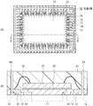
図5(A)はリードフレーム10の表面、図5(B)はその裏面の平面構成をそれぞれ表すものである。図5のドットで表した領域は、図5(A)は表面から、図5(B)は裏面からそれぞれ一定の厚みだけ削られ、他の部分に比べて薄くなっている箇所を表している。
リードフレーム10は、例えばメッキされた銅(Cu)により構成され、チップ搭載領域11(ダイパッド)、端子12(信号端子)、リード領域13Aおよび端子12とリード領域13Aとの間の間隙14を有している。間隙14と端子12との間には端子12を支持する張出部15(図2)が設けられている。図5(A)のドット領域は張出部15、図5(B)のドット領域はリード領域13Aである。
続いて、封止樹脂41の表面に製品名等のマーク54を刻印した後(図12)、図13に表したようにカッター等により切断線55でリードフレームシートからリードフレーム10を切り離す。以上の工程により、図1〜4に示した半導体装置1が完成する。
半導体チップ21A,21B,21Cは互いの電極パッド同士がワイヤ31により電気的に接続され、リードフレーム10(チップ搭載領域11)に搭載されている。即ち、この半導体装置2は所謂マルチチップの構成を有するものである。
Priority Applications (3)
| Application Number | Priority Date | Filing Date | Title |
|---|---|---|---|
| JP2011239444A JP5953703B2 (ja) | 2011-10-31 | 2011-10-31 | リードフレームおよび半導体装置 |
| CN201210423881.9A CN103094238B (zh) | 2011-10-31 | 2012-10-24 | 引线框架和半导体器件 |
| US13/659,557 US8928136B2 (en) | 2011-10-31 | 2012-10-24 | Lead frame semiconductor device |
Applications Claiming Priority (1)
| Application Number | Priority Date | Filing Date | Title |
|---|---|---|---|
| JP2011239444A JP5953703B2 (ja) | 2011-10-31 | 2011-10-31 | リードフレームおよび半導体装置 |
Publications (3)
| Publication Number | Publication Date |
|---|---|
| JP2013098332A JP2013098332A (ja) | 2013-05-20 |
| JP2013098332A5 true JP2013098332A5 (ja) | 2014-11-27 |
| JP5953703B2 JP5953703B2 (ja) | 2016-07-20 |
Family
ID=48171542
Family Applications (1)
| Application Number | Title | Priority Date | Filing Date |
|---|---|---|---|
| JP2011239444A Expired - Fee Related JP5953703B2 (ja) | 2011-10-31 | 2011-10-31 | リードフレームおよび半導体装置 |
Country Status (3)
| Country | Link |
|---|---|
| US (1) | US8928136B2 (ja) |
| JP (1) | JP5953703B2 (ja) |
| CN (1) | CN103094238B (ja) |
Families Citing this family (10)
| Publication number | Priority date | Publication date | Assignee | Title |
|---|---|---|---|---|
| JP6352009B2 (ja) * | 2013-04-16 | 2018-07-04 | ローム株式会社 | 半導体装置 |
| CN103337488B (zh) * | 2013-06-05 | 2016-09-14 | 吉林华微斯帕克电气有限公司 | 一种引线框架 |
| JP6413709B2 (ja) * | 2014-12-02 | 2018-10-31 | 富士電機株式会社 | 半導体装置およびその製造方法 |
| US9966326B2 (en) * | 2015-03-16 | 2018-05-08 | Unisem (M) Berhad | Lead frames with wettable flanks |
| JP6507779B2 (ja) * | 2015-03-26 | 2019-05-08 | セイコーエプソン株式会社 | 電気光学装置、電気光学装置の製造方法、および電子機器 |
| JP6555927B2 (ja) * | 2015-05-18 | 2019-08-07 | 大口マテリアル株式会社 | 半導体素子搭載用リードフレーム及び半導体装置の製造方法 |
| JP6772087B2 (ja) * | 2017-02-17 | 2020-10-21 | 新光電気工業株式会社 | リードフレーム及びその製造方法 |
| US10679929B2 (en) * | 2017-07-28 | 2020-06-09 | Advanced Semiconductor Engineering Korea, Inc. | Semiconductor package device and method of manufacturing the same |
| US20190221502A1 (en) * | 2018-01-17 | 2019-07-18 | Microchip Technology Incorporated | Down Bond in Semiconductor Devices |
| CN110828442A (zh) * | 2019-11-04 | 2020-02-21 | 弘凯光电(深圳)有限公司 | 封装结构及其制作方法 |
Family Cites Families (28)
| Publication number | Priority date | Publication date | Assignee | Title |
|---|---|---|---|---|
| US5084753A (en) * | 1989-01-23 | 1992-01-28 | Analog Devices, Inc. | Packaging for multiple chips on a single leadframe |
| JPH0621319A (ja) * | 1992-06-30 | 1994-01-28 | Nec Corp | 半導体装置用リードフレーム |
| JP2811170B2 (ja) * | 1996-06-28 | 1998-10-15 | 株式会社後藤製作所 | 樹脂封止型半導体装置及びその製造方法 |
| DE19808193B4 (de) * | 1998-02-27 | 2007-11-08 | Robert Bosch Gmbh | Leadframevorrichtung und entsprechendes Herstellungsverfahren |
| JPH11340405A (ja) * | 1998-05-22 | 1999-12-10 | Fujitsu Quantum Devices Kk | リードフレーム、半導体装置およびその製造方法 |
| KR100526844B1 (ko) * | 1999-10-15 | 2005-11-08 | 앰코 테크놀로지 코리아 주식회사 | 반도체패키지 및 그 제조방법 |
| US6198171B1 (en) * | 1999-12-30 | 2001-03-06 | Siliconware Precision Industries Co., Ltd. | Thermally enhanced quad flat non-lead package of semiconductor |
| TW447059B (en) * | 2000-04-28 | 2001-07-21 | Siliconware Precision Industries Co Ltd | Multi-chip module integrated circuit package |
| JP2001313363A (ja) * | 2000-05-01 | 2001-11-09 | Rohm Co Ltd | 樹脂封止型半導体装置 |
| JP2002026190A (ja) * | 2000-07-03 | 2002-01-25 | Dainippon Printing Co Ltd | 樹脂封止型半導体装置 |
| US6661082B1 (en) * | 2000-07-19 | 2003-12-09 | Fairchild Semiconductor Corporation | Flip chip substrate design |
| JP3895570B2 (ja) * | 2000-12-28 | 2007-03-22 | 株式会社ルネサステクノロジ | 半導体装置 |
| US6720207B2 (en) * | 2001-02-14 | 2004-04-13 | Matsushita Electric Industrial Co., Ltd. | Leadframe, resin-molded semiconductor device including the leadframe, method of making the leadframe and method for manufacturing the device |
| JP2003204027A (ja) * | 2002-01-09 | 2003-07-18 | Matsushita Electric Ind Co Ltd | リードフレーム及びその製造方法、樹脂封止型半導体装置及びその製造方法 |
| CN100380651C (zh) | 2002-04-30 | 2008-04-09 | 株式会社瑞萨科技 | 半导体器件和电子设备 |
| KR100975692B1 (ko) * | 2002-07-01 | 2010-08-12 | 가부시끼가이샤 르네사스 테크놀로지 | 반도체 장치 |
| JP2004071801A (ja) * | 2002-08-06 | 2004-03-04 | Shinko Electric Ind Co Ltd | リードフレーム及びその製造方法 |
| US20040124508A1 (en) * | 2002-11-27 | 2004-07-01 | United Test And Assembly Test Center Ltd. | High performance chip scale leadframe package and method of manufacturing the package |
| JP2005057067A (ja) * | 2003-08-05 | 2005-03-03 | Renesas Technology Corp | 半導体装置およびその製造方法 |
| JP2005191342A (ja) * | 2003-12-26 | 2005-07-14 | Renesas Technology Corp | 半導体装置およびその製造方法 |
| US7247937B2 (en) * | 2005-01-06 | 2007-07-24 | Via Technologies, Inc. | Mounting pad structure for wire-bonding type lead frame packages |
| JP2007012857A (ja) * | 2005-06-30 | 2007-01-18 | Renesas Technology Corp | 半導体装置 |
| US7301225B2 (en) * | 2006-02-28 | 2007-11-27 | Freescale Semiconductor, Inc. | Multi-row lead frame |
| JP4652281B2 (ja) | 2006-05-29 | 2011-03-16 | パナソニック株式会社 | 樹脂封止型半導体装置 |
| US7556987B2 (en) * | 2006-06-30 | 2009-07-07 | Stats Chippac Ltd. | Method of fabricating an integrated circuit with etched ring and die paddle |
| EP2084744A2 (en) * | 2006-10-27 | 2009-08-05 | Unisem (Mauritius) Holdings Limited | Partially patterned lead frames and methods of making and using the same in semiconductor packaging |
| CN101308832B (zh) * | 2007-05-17 | 2010-06-16 | 南茂科技股份有限公司 | 用于无引线封装的引线框、其封装结构及其制造方法 |
| JP5184558B2 (ja) * | 2010-01-18 | 2013-04-17 | ルネサスエレクトロニクス株式会社 | 半導体装置 |
-
2011
- 2011-10-31 JP JP2011239444A patent/JP5953703B2/ja not_active Expired - Fee Related
-
2012
- 2012-10-24 CN CN201210423881.9A patent/CN103094238B/zh not_active Expired - Fee Related
- 2012-10-24 US US13/659,557 patent/US8928136B2/en not_active Expired - Fee Related
Similar Documents
| Publication | Publication Date | Title |
|---|---|---|
| JP2013098332A5 (ja) | ||
| CN103681577B (zh) | 树脂密封型半导体装置及其制造方法 | |
| JP5634033B2 (ja) | 樹脂封止型半導体装置とその製造方法 | |
| TW201119004A (en) | Semiconductor device packages and manufacturing method thereof | |
| TW201001658A (en) | Foil based semiconductor package | |
| EP2654388A3 (en) | Semiconductor package, semiconductor apparatus and method for manufacturing semiconductor package | |
| JP2015504608A5 (ja) | ||
| GB201020062D0 (en) | Multi-chip package | |
| JP2008258411A5 (ja) | ||
| JP2014220439A5 (ja) | ||
| JP2016503240A5 (ja) | ||
| US9437528B1 (en) | Dual-side exposed semiconductor package with ultra-thin die and manufacturing method thereof | |
| JP2016119366A5 (ja) | ||
| TWI833739B (zh) | 半導體封裝及製造其之方法 | |
| JP2013098332A (ja) | リードフレームおよび半導体装置 | |
| JP2010258200A (ja) | 半導体装置およびその製造方法 | |
| EP2472616A3 (en) | Light-emitting device package and method of manufacturing the same | |
| JP2006196922A5 (ja) | ||
| US20160307831A1 (en) | Method of making a qfn package | |
| KR101594492B1 (ko) | 반도체 패키지 구조물 및 그 제작 방법 | |
| JP2007129068A (ja) | 半導体装置とその製造方法、及びその製造に用いる基板 | |
| TW201130096A (en) | Chip scale semiconductor device package and manufacturing method thereof | |
| US9418920B2 (en) | Integrated circuit (IC) package with thick die pad functioning as a heat sink | |
| JP6120629B2 (ja) | チップ抵抗器、およびチップ抵抗器の製造方法 | |
| JP2009065201A5 (ja) |