JP2009295932A - 露光装置及びデバイス製造方法 - Google Patents
露光装置及びデバイス製造方法 Download PDFInfo
- Publication number
- JP2009295932A JP2009295932A JP2008150836A JP2008150836A JP2009295932A JP 2009295932 A JP2009295932 A JP 2009295932A JP 2008150836 A JP2008150836 A JP 2008150836A JP 2008150836 A JP2008150836 A JP 2008150836A JP 2009295932 A JP2009295932 A JP 2009295932A
- Authority
- JP
- Japan
- Prior art keywords
- substrate
- measurement
- stage
- exposure
- exposure apparatus
- Prior art date
- Legal status (The legal status is an assumption and is not a legal conclusion. Google has not performed a legal analysis and makes no representation as to the accuracy of the status listed.)
- Pending
Links
Images


Classifications
-
- G—PHYSICS
- G03—PHOTOGRAPHY; CINEMATOGRAPHY; ANALOGOUS TECHNIQUES USING WAVES OTHER THAN OPTICAL WAVES; ELECTROGRAPHY; HOLOGRAPHY
- G03F—PHOTOMECHANICAL PRODUCTION OF TEXTURED OR PATTERNED SURFACES, e.g. FOR PRINTING, FOR PROCESSING OF SEMICONDUCTOR DEVICES; MATERIALS THEREFOR; ORIGINALS THEREFOR; APPARATUS SPECIALLY ADAPTED THEREFOR
- G03F7/00—Photomechanical, e.g. photolithographic, production of textured or patterned surfaces, e.g. printing surfaces; Materials therefor, e.g. comprising photoresists; Apparatus specially adapted therefor
- G03F7/70—Microphotolithographic exposure; Apparatus therefor
- G03F7/70483—Information management; Active and passive control; Testing; Wafer monitoring, e.g. pattern monitoring
- G03F7/70491—Information management, e.g. software; Active and passive control, e.g. details of controlling exposure processes or exposure tool monitoring processes
- G03F7/70508—Data handling in all parts of the microlithographic apparatus, e.g. handling pattern data for addressable masks or data transfer to or from different components within the exposure apparatus
-
- G—PHYSICS
- G03—PHOTOGRAPHY; CINEMATOGRAPHY; ANALOGOUS TECHNIQUES USING WAVES OTHER THAN OPTICAL WAVES; ELECTROGRAPHY; HOLOGRAPHY
- G03F—PHOTOMECHANICAL PRODUCTION OF TEXTURED OR PATTERNED SURFACES, e.g. FOR PRINTING, FOR PROCESSING OF SEMICONDUCTOR DEVICES; MATERIALS THEREFOR; ORIGINALS THEREFOR; APPARATUS SPECIALLY ADAPTED THEREFOR
- G03F7/00—Photomechanical, e.g. photolithographic, production of textured or patterned surfaces, e.g. printing surfaces; Materials therefor, e.g. comprising photoresists; Apparatus specially adapted therefor
- G03F7/70—Microphotolithographic exposure; Apparatus therefor
- G03F7/70216—Mask projection systems
- G03F7/70358—Scanning exposure, i.e. relative movement of patterned beam and workpiece during imaging
-
- G—PHYSICS
- G03—PHOTOGRAPHY; CINEMATOGRAPHY; ANALOGOUS TECHNIQUES USING WAVES OTHER THAN OPTICAL WAVES; ELECTROGRAPHY; HOLOGRAPHY
- G03F—PHOTOMECHANICAL PRODUCTION OF TEXTURED OR PATTERNED SURFACES, e.g. FOR PRINTING, FOR PROCESSING OF SEMICONDUCTOR DEVICES; MATERIALS THEREFOR; ORIGINALS THEREFOR; APPARATUS SPECIALLY ADAPTED THEREFOR
- G03F7/00—Photomechanical, e.g. photolithographic, production of textured or patterned surfaces, e.g. printing surfaces; Materials therefor, e.g. comprising photoresists; Apparatus specially adapted therefor
- G03F7/70—Microphotolithographic exposure; Apparatus therefor
- G03F7/70483—Information management; Active and passive control; Testing; Wafer monitoring, e.g. pattern monitoring
- G03F7/70491—Information management, e.g. software; Active and passive control, e.g. details of controlling exposure processes or exposure tool monitoring processes
- G03F7/70525—Controlling normal operating mode, e.g. matching different apparatus, remote control or prediction of failure
-
- G—PHYSICS
- G03—PHOTOGRAPHY; CINEMATOGRAPHY; ANALOGOUS TECHNIQUES USING WAVES OTHER THAN OPTICAL WAVES; ELECTROGRAPHY; HOLOGRAPHY
- G03F—PHOTOMECHANICAL PRODUCTION OF TEXTURED OR PATTERNED SURFACES, e.g. FOR PRINTING, FOR PROCESSING OF SEMICONDUCTOR DEVICES; MATERIALS THEREFOR; ORIGINALS THEREFOR; APPARATUS SPECIALLY ADAPTED THEREFOR
- G03F7/00—Photomechanical, e.g. photolithographic, production of textured or patterned surfaces, e.g. printing surfaces; Materials therefor, e.g. comprising photoresists; Apparatus specially adapted therefor
- G03F7/70—Microphotolithographic exposure; Apparatus therefor
- G03F7/70691—Handling of masks or workpieces
- G03F7/70716—Stages
- G03F7/70725—Stages control
-
- G—PHYSICS
- G03—PHOTOGRAPHY; CINEMATOGRAPHY; ANALOGOUS TECHNIQUES USING WAVES OTHER THAN OPTICAL WAVES; ELECTROGRAPHY; HOLOGRAPHY
- G03F—PHOTOMECHANICAL PRODUCTION OF TEXTURED OR PATTERNED SURFACES, e.g. FOR PRINTING, FOR PROCESSING OF SEMICONDUCTOR DEVICES; MATERIALS THEREFOR; ORIGINALS THEREFOR; APPARATUS SPECIALLY ADAPTED THEREFOR
- G03F7/00—Photomechanical, e.g. photolithographic, production of textured or patterned surfaces, e.g. printing surfaces; Materials therefor, e.g. comprising photoresists; Apparatus specially adapted therefor
- G03F7/70—Microphotolithographic exposure; Apparatus therefor
- G03F7/70691—Handling of masks or workpieces
- G03F7/70775—Position control, e.g. interferometers or encoders for determining the stage position
-
- H—ELECTRICITY
- H01—ELECTRIC ELEMENTS
- H01L—SEMICONDUCTOR DEVICES NOT COVERED BY CLASS H10
- H01L21/00—Processes or apparatus adapted for the manufacture or treatment of semiconductor or solid state devices or of parts thereof
- H01L21/67—Apparatus specially adapted for handling semiconductor or electric solid state devices during manufacture or treatment thereof; Apparatus specially adapted for handling wafers during manufacture or treatment of semiconductor or electric solid state devices or components ; Apparatus not specifically provided for elsewhere
- H01L21/67005—Apparatus not specifically provided for elsewhere
- H01L21/67242—Apparatus for monitoring, sorting or marking
- H01L21/67259—Position monitoring, e.g. misposition detection or presence detection
Landscapes
- Physics & Mathematics (AREA)
- General Physics & Mathematics (AREA)
- Engineering & Computer Science (AREA)
- Condensed Matter Physics & Semiconductors (AREA)
- Manufacturing & Machinery (AREA)
- Computer Hardware Design (AREA)
- Microelectronics & Electronic Packaging (AREA)
- Power Engineering (AREA)
- Exposure Of Semiconductors, Excluding Electron Or Ion Beam Exposure (AREA)
- Exposure And Positioning Against Photoresist Photosensitive Materials (AREA)
- Container, Conveyance, Adherence, Positioning, Of Wafer (AREA)
Abstract
【解決手段】駆動機構は、基板を保持する基板ステージを、投影光学系の光軸方向と直交する第1方向に走査移動させ、光軸方向及び第1方向に直交する第2方向にステップ移動させる。第1計測器は、駆動機構が基板ステージを第1方向に走査移動させるときに、投影光学系の光軸方向における基板ステージの位置を計測する。第2計測器は、基板の上で第2方向に延びる一つの直線上に位置する複数の計測点で投影光学系の光軸方向における基板の表面位置を計測する。制御器は、基板ステージが第2方向にステップ移動する前と後との双方において、基板の少なくとも1つの同一の領域を第2計測器に複数の計測点7−1〜6の中の互いに異なる計測点で計測させ、第2計測器による計測結果に基づいて基板ステージの第2方向に沿った移動に伴う第1計測器の計測誤差を算出する。
【選択図】図11
Description
前記基板を保持する基板ステージを、前記投影光学系の光軸方向と直交する第1方向に走査移動させ、前記光軸方向及び前記第1方向に直交する第2方向にステップ移動させる駆動機構と、
前記駆動機構が前記基板ステージを前記第1方向に走査移動させるときに、前記投影光学系の光軸方向における前記基板ステージの位置を計測する第1計測器と、
前記基板の上で前記第2方向に延びる一つの直線上に位置する複数の計測点で前記投影光学系の光軸方向における前記基板の表面位置を計測する第2計測器と、
制御器と、
を備え、
前記制御器は、前記基板ステージが前記第2方向にステップ移動する前と後との双方において、基板の少なくとも1つの同一の領域を前記第2計測器に前記複数の計測点の中の互いに異なる計測点で計測させ、当該第2計測器による計測結果に基づいて前記基板ステージの第2方向に沿った移動に伴う前記第1計測器の計測誤差を算出する、ことを特徴とする。
ツインステージ構成の露光装置は、露光領域と、計測領域と、露光領域及び計測領域を移動可能な複数の基板ステージとを有し、計測領域で計測された基板をその計測結果に従って位置決めしながら露光領域で露光する。
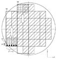
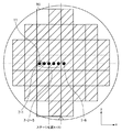
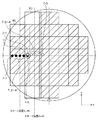
次に、隣接する領域9Bを計測する場合、左端の計測点7−1が、先の領域9Aを計測したときに右端の計測点7−6が計測した位置と同じ位置(図11の11)であるようにする。領域9Bを計測するときの計測点7−1の計測値をA(X1)とし、計測点7−6の計測値をB(X1)とする。
B(X0)
B(X1)、 A(X1)
B(X2)、 A(X2)
:
B(Xn―1)、A(Xn―1)
A(Xn)
このとき、X0〜Xnは以下の関係にある。
X1=X0+XF
X2=X1+XF=X0+2XF
:
Xn=Xn−1+XF=X0+nXF
ここで、XFは、フォーカス計測領域の幅であり、隣接する領域を計測するために、基板ステージがステップ移動する幅である。
ΔZ(X0→X1)=A(X1)−B(X0)
ΔZ(X1→X2)=A(X2)−B(X1)
:
ΔZ(Xn−1→Xn)=A(Xn)−B(Xn−1)
上記式は、基板ステージが、XFだけ駆動したときの、誤差の差分を示している。これを、ZXのバーミラーの絶対値Z(X0〜Xn)に変換するためには、上記を累積していけばよい。このとき、絶対値の基準がないため、とりあえず、基板ステージがX0のときにおけるバーミラーの誤差成分を0と仮定する。
Z(X0)=0
Z(X1)=Z(X0)+ΔZ(X0→X1)=0+ΔZ(X0→X1)
Z(X2)=Z(X1)+ΔZ(X1→X2)=0+ΔZ(X0→X1)+ΔZ(X1→X2)
:
Z(Xn)=Z(Xn−1)+ΔZ(Xn−1→Xn)=ΔZ(X0→X1)+・・・+ΔZ(Xn−1→Xn)
ここで、X=X0を、ZXバーミラーの形状を判断する基準としたが、これは、計算の便宜上であり、どこを基準としても問題はない。たとえば、X=Xcを、ZXバーミラーの形状を判断する基準としたい場合、全配列から、Z(Xc)の値を引いてやればよい。その場合には、以下のようになる。
Z(X0)→Z(X0)―Z(Xc)
Z(X1)→Z(X1)―Z(Xc)
:
Z(Xc)→Z(Xc)―Z(Xc)=0
:
Z(Xn)→Z(Xn)―Z(Xc)
ここで得られるZXバーミラーの形状は、あくまで、前回、計測・補正してからの変化量である。つまり、ZXバーミラーが変化していなければ、上記関数Z(X)は、0か、計測誤差程度のごく小さい値となる。
次に、シングルステージ構成の露光装置で用いられる、露光直前にフォーカス計測する場合について、説明する。
B(X0)、 S(X0)
B(X1)、 A(X1)、 S(X1)
B(X2)、 A(X2)、 S(X2)
:
B(Xn−1)、A(Xn−1)、S(Xn−1)
A(Xn)、 S(Xn)
Z誤差ΔZは基板ステージの駆動量を考慮して以下のようになる。
ΔZ(X0→X1)={A(X1)−S(X1)}−{B(X0)−S(X0)}
ΔZ(X1→X2)={A(X2)−S(X2)}−{B(X1)−S(X1)}
:
ΔZ(Xn−1→Xn)={A(Xn)−S(Xn)}−{B(Xn−1)−S(Xn−1)}
シングルステージ構成においても、ツインステージ構成と全く同様に、基板全面におけるZバーミラーの形状を算出することができる。
S(X)=Zs(X)+Tilt−X(X)・Xrot(X)+Tilt−Y(X)・Yrot(X)
各X位置(X0,X1,・・・Xn)において、上記式を適応すればよい。
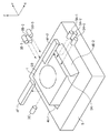
本発明で適用される例示的なシングルステージ構成の露光装置を説明する。露光装置は図15に示すように、照明装置101、レチクルを搭載したレチクルステージ102、投影光学系103、基板を保持する基板ステージ1とを備える。上述したように基板ステージ1は、不図示の駆動機構によってY方向に操作移動され、X方向にステップ移動される。露光装置は、レチクルに形成された回路パターンを基板に投影して走査露光する。
2A:Xバーミラー
2B:Yバーミラー
3A−1:Xレーザ干渉計
3A−2:チルトレーザ干渉計
3A−3:ヨーレーザ干渉計
3B−1:Yレーザ干渉計
3B−2:チルトレーザ干渉計
3B−3:ヨーレーザ干渉計
4A:45度ミラー
4B:45度バーミラー
4C:ZXバーミラー
4D:ZYバーミラー
4E−1:ZYバーミラー(ZYL)
4E−2:ZYバーミラー(ZYR)
4F−1:ZXバーミラー(ZXL)
4F−2:ZXバーミラー(ZXR)
5:基板ステージ定盤
6A−1〜4:フォーカスセンサ(先読み)の計測点
6B−1〜4:フォーカスセンサ(中心)の計測点
6C−1〜4:フォーカスセンサ(先読み)の計測点
7−1〜6:フォーカスセンサの計測点
8:Y計測用フォーカスセンサ
9A:フォーカス計測領域
9B:隣接したフォーカス計測領域
9C:フォーカス計測領域
9D:隣接したフォーカス計測領域
11:重複して計測される基板上の位置
12−1:露光領域1
12−2:隣接した露光領域2
13:重複して計測される基板上の位置
Claims (10)
- 投影光学系を介してレチクルのパターンを基板に投影して前記基板を走査露光する露光装置であって、
前記基板を保持する基板ステージを、前記投影光学系の光軸方向と直交する第1方向に走査移動させ、前記光軸方向及び前記第1方向に直交する第2方向にステップ移動させる駆動機構と、
前記駆動機構が前記基板ステージを前記第1方向に走査移動させるときに、前記投影光学系の光軸方向における前記基板ステージの位置を計測する第1計測器と、
前記基板の上で前記第2方向に延びる一つの直線上に位置する複数の計測点で前記投影光学系の光軸方向における前記基板の表面位置を計測する第2計測器と、
制御器と、
を備え、
前記制御器は、前記基板ステージが前記第2方向にステップ移動する前と後との双方において、基板の少なくとも1つの同一の領域を前記第2計測器に前記複数の計測点の中の互いに異なる計測点で計測させ、当該第2計測器による計測結果に基づいて前記基板ステージの第2方向に沿った移動に伴う前記第1計測器の計測誤差を算出する、ことを特徴とする露光装置。 - 前記制御器は、前記第1計測器の計測誤差を算出するモードにおいて、前記第2計測器が基板の少なくとも1つの同一の領域を互いに異なる計測点で計測できるように、前記基板ステージが前記第2方向にステップ移動する幅を小さくすることを特徴とする請求項1に記載の露光装置。
- 前記制御器は、前記算出した第1計測器の計測誤差を用いて前記第1計測器の計測結果を補正することを特徴とする請求項1又は請求項2に記載の露光装置。
- 前記第1計測器は、バーミラー及び干渉計を含み、
前記制御器は、前記算出した第1計測器の計測誤差に基づいて前記バーミラーを計測する時期を決定することを特徴とする請求項1乃至請求項3のいずれか1項に記載の露光装置。 - 前記第2計測器は、基板の少なくとも1つの同一の領域における互いに異なる計測点での前記計測を、前記露光装置の電源を投入したとき、前記基板ステージの原点位置を決定するとき、又は、露光処理を行うロットの最初の基板が前記基板ステージに搭載されたときに行うことを特徴とする請求項1乃至請求項4のいずれか1項に記載の露光装置。
- 前記第2計測器は、基板の少なくとも1つの同一の領域における互いに異なる計測点での前記計測を、予め定められた枚数の基板が処理される毎に、又は、予め定められた時間が経過する毎に行うことを特徴とする請求項1乃至請求項4のいずれか1項に記載の露光装置。
- 前記第2計測器は、基板の少なくとも1つの同一の領域におけるする互いに異なる計測点での前記計測を、下地のパターンを有さない基板に対して行うことを特徴とする請求項1乃至請求項4のいずれか1項に記載の露光装置。
- 前記露光装置は、投影光学系を介して基板を露光する露光領域と、基板を計測する計測領域と、前記露光領域及び前記計測領域を移動可能な複数の基板ステージとを有し、前記計測領域で計測された基板をその計測結果に従って位置決めしながら前記露光領域で露光する露光装置であって、
前記第1計測器と前記第2計測器とは前記計測領域に配置されていることを特徴とする請求項1乃至請求項7のいずれか1項に記載の露光装置。 - 前記露光装置は、基板を前記第1計測器の計測結果に基づいて位置決めしながら露光することを特徴とする請求項1乃至請求項7のいずれか1項に記載の露光装置。
- 請求項1乃至請求項9のいずれか1項に記載の露光装置を用いて基板を露光する工程と、
前記工程で露光された基板を現像する工程と、
を含むデバイス製造方法。
Priority Applications (4)
| Application Number | Priority Date | Filing Date | Title |
|---|---|---|---|
| JP2008150836A JP2009295932A (ja) | 2008-06-09 | 2008-06-09 | 露光装置及びデバイス製造方法 |
| US12/469,118 US7884918B2 (en) | 2008-06-09 | 2009-05-20 | Exposure apparatus and method of manufacturing device |
| TW098118211A TW201007373A (en) | 2008-06-09 | 2009-06-02 | Exposure apparatus and method of manufacturing device |
| KR1020090050948A KR101124730B1 (ko) | 2008-06-09 | 2009-06-09 | 노광 장치 및 디바이스 제조 방법 |
Applications Claiming Priority (1)
| Application Number | Priority Date | Filing Date | Title |
|---|---|---|---|
| JP2008150836A JP2009295932A (ja) | 2008-06-09 | 2008-06-09 | 露光装置及びデバイス製造方法 |
Publications (2)
| Publication Number | Publication Date |
|---|---|
| JP2009295932A true JP2009295932A (ja) | 2009-12-17 |
| JP2009295932A5 JP2009295932A5 (ja) | 2011-07-21 |
Family
ID=41400630
Family Applications (1)
| Application Number | Title | Priority Date | Filing Date |
|---|---|---|---|
| JP2008150836A Pending JP2009295932A (ja) | 2008-06-09 | 2008-06-09 | 露光装置及びデバイス製造方法 |
Country Status (4)
| Country | Link |
|---|---|
| US (1) | US7884918B2 (ja) |
| JP (1) | JP2009295932A (ja) |
| KR (1) | KR101124730B1 (ja) |
| TW (1) | TW201007373A (ja) |
Cited By (2)
| Publication number | Priority date | Publication date | Assignee | Title |
|---|---|---|---|---|
| JP2016502070A (ja) * | 2012-10-24 | 2016-01-21 | エーエスエムエル ネザーランズ ビー.ブイ. | オブジェクト位置決めシステム、リソグラフィ装置、およびデバイス製造方法 |
| JP7475185B2 (ja) | 2020-04-10 | 2024-04-26 | キヤノン株式会社 | 計測方法、インプリント装置及び物品の製造方法 |
Families Citing this family (345)
| Publication number | Priority date | Publication date | Assignee | Title |
|---|---|---|---|---|
| US8986456B2 (en) * | 2006-10-10 | 2015-03-24 | Asm America, Inc. | Precursor delivery system |
| US10378106B2 (en) | 2008-11-14 | 2019-08-13 | Asm Ip Holding B.V. | Method of forming insulation film by modified PEALD |
| US9394608B2 (en) | 2009-04-06 | 2016-07-19 | Asm America, Inc. | Semiconductor processing reactor and components thereof |
| US8883270B2 (en) * | 2009-08-14 | 2014-11-11 | Asm America, Inc. | Systems and methods for thin-film deposition of metal oxides using excited nitrogen—oxygen species |
| US8877655B2 (en) | 2010-05-07 | 2014-11-04 | Asm America, Inc. | Systems and methods for thin-film deposition of metal oxides using excited nitrogen-oxygen species |
| US8802201B2 (en) | 2009-08-14 | 2014-08-12 | Asm America, Inc. | Systems and methods for thin-film deposition of metal oxides using excited nitrogen-oxygen species |
| US9312155B2 (en) | 2011-06-06 | 2016-04-12 | Asm Japan K.K. | High-throughput semiconductor-processing apparatus equipped with multiple dual-chamber modules |
| US9793148B2 (en) | 2011-06-22 | 2017-10-17 | Asm Japan K.K. | Method for positioning wafers in multiple wafer transport |
| US10364496B2 (en) | 2011-06-27 | 2019-07-30 | Asm Ip Holding B.V. | Dual section module having shared and unshared mass flow controllers |
| US10854498B2 (en) | 2011-07-15 | 2020-12-01 | Asm Ip Holding B.V. | Wafer-supporting device and method for producing same |
| US20130023129A1 (en) | 2011-07-20 | 2013-01-24 | Asm America, Inc. | Pressure transmitter for a semiconductor processing environment |
| NL2009197A (en) * | 2011-08-25 | 2013-02-27 | Asml Netherlands Bv | System for detection motion, lithographic apparatus and device manufacturing method. |
| US9341296B2 (en) | 2011-10-27 | 2016-05-17 | Asm America, Inc. | Heater jacket for a fluid line |
| US9096931B2 (en) | 2011-10-27 | 2015-08-04 | Asm America, Inc | Deposition valve assembly and method of heating the same |
| US9017481B1 (en) | 2011-10-28 | 2015-04-28 | Asm America, Inc. | Process feed management for semiconductor substrate processing |
| US9005539B2 (en) | 2011-11-23 | 2015-04-14 | Asm Ip Holding B.V. | Chamber sealing member |
| US9167625B2 (en) | 2011-11-23 | 2015-10-20 | Asm Ip Holding B.V. | Radiation shielding for a substrate holder |
| US9202727B2 (en) | 2012-03-02 | 2015-12-01 | ASM IP Holding | Susceptor heater shim |
| CN103309167B (zh) * | 2012-03-09 | 2015-06-17 | 上海微电子装备有限公司 | 运动台定位精度的测量系统及测量方法 |
| US8946830B2 (en) | 2012-04-04 | 2015-02-03 | Asm Ip Holdings B.V. | Metal oxide protective layer for a semiconductor device |
| US9029253B2 (en) | 2012-05-02 | 2015-05-12 | Asm Ip Holding B.V. | Phase-stabilized thin films, structures and devices including the thin films, and methods of forming same |
| US8728832B2 (en) | 2012-05-07 | 2014-05-20 | Asm Ip Holdings B.V. | Semiconductor device dielectric interface layer |
| US8933375B2 (en) | 2012-06-27 | 2015-01-13 | Asm Ip Holding B.V. | Susceptor heater and method of heating a substrate |
| US9558931B2 (en) | 2012-07-27 | 2017-01-31 | Asm Ip Holding B.V. | System and method for gas-phase sulfur passivation of a semiconductor surface |
| JP6066610B2 (ja) * | 2012-07-31 | 2017-01-25 | キヤノン株式会社 | 露光方法、露光装置及びデバイス製造方法 |
| US9117866B2 (en) * | 2012-07-31 | 2015-08-25 | Asm Ip Holding B.V. | Apparatus and method for calculating a wafer position in a processing chamber under process conditions |
| US9659799B2 (en) | 2012-08-28 | 2017-05-23 | Asm Ip Holding B.V. | Systems and methods for dynamic semiconductor process scheduling |
| US9169975B2 (en) | 2012-08-28 | 2015-10-27 | Asm Ip Holding B.V. | Systems and methods for mass flow controller verification |
| US9021985B2 (en) | 2012-09-12 | 2015-05-05 | Asm Ip Holdings B.V. | Process gas management for an inductively-coupled plasma deposition reactor |
| US9324811B2 (en) | 2012-09-26 | 2016-04-26 | Asm Ip Holding B.V. | Structures and devices including a tensile-stressed silicon arsenic layer and methods of forming same |
| US10714315B2 (en) | 2012-10-12 | 2020-07-14 | Asm Ip Holdings B.V. | Semiconductor reaction chamber showerhead |
| US9640416B2 (en) | 2012-12-26 | 2017-05-02 | Asm Ip Holding B.V. | Single-and dual-chamber module-attachable wafer-handling chamber |
| US20160376700A1 (en) | 2013-02-01 | 2016-12-29 | Asm Ip Holding B.V. | System for treatment of deposition reactor |
| US8894870B2 (en) | 2013-02-01 | 2014-11-25 | Asm Ip Holding B.V. | Multi-step method and apparatus for etching compounds containing a metal |
| US9589770B2 (en) | 2013-03-08 | 2017-03-07 | Asm Ip Holding B.V. | Method and systems for in-situ formation of intermediate reactive species |
| US9484191B2 (en) | 2013-03-08 | 2016-11-01 | Asm Ip Holding B.V. | Pulsed remote plasma method and system |
| US8993054B2 (en) | 2013-07-12 | 2015-03-31 | Asm Ip Holding B.V. | Method and system to reduce outgassing in a reaction chamber |
| US9018111B2 (en) | 2013-07-22 | 2015-04-28 | Asm Ip Holding B.V. | Semiconductor reaction chamber with plasma capabilities |
| US9793115B2 (en) | 2013-08-14 | 2017-10-17 | Asm Ip Holding B.V. | Structures and devices including germanium-tin films and methods of forming same |
| US9396934B2 (en) | 2013-08-14 | 2016-07-19 | Asm Ip Holding B.V. | Methods of forming films including germanium tin and structures and devices including the films |
| US9240412B2 (en) | 2013-09-27 | 2016-01-19 | Asm Ip Holding B.V. | Semiconductor structure and device and methods of forming same using selective epitaxial process |
| US9556516B2 (en) | 2013-10-09 | 2017-01-31 | ASM IP Holding B.V | Method for forming Ti-containing film by PEALD using TDMAT or TDEAT |
| US9605343B2 (en) | 2013-11-13 | 2017-03-28 | Asm Ip Holding B.V. | Method for forming conformal carbon films, structures conformal carbon film, and system of forming same |
| US10179947B2 (en) | 2013-11-26 | 2019-01-15 | Asm Ip Holding B.V. | Method for forming conformal nitrided, oxidized, or carbonized dielectric film by atomic layer deposition |
| US10683571B2 (en) | 2014-02-25 | 2020-06-16 | Asm Ip Holding B.V. | Gas supply manifold and method of supplying gases to chamber using same |
| US9447498B2 (en) | 2014-03-18 | 2016-09-20 | Asm Ip Holding B.V. | Method for performing uniform processing in gas system-sharing multiple reaction chambers |
| US10167557B2 (en) | 2014-03-18 | 2019-01-01 | Asm Ip Holding B.V. | Gas distribution system, reactor including the system, and methods of using the same |
| US11015245B2 (en) | 2014-03-19 | 2021-05-25 | Asm Ip Holding B.V. | Gas-phase reactor and system having exhaust plenum and components thereof |
| US9404587B2 (en) | 2014-04-24 | 2016-08-02 | ASM IP Holding B.V | Lockout tagout for semiconductor vacuum valve |
| US10858737B2 (en) | 2014-07-28 | 2020-12-08 | Asm Ip Holding B.V. | Showerhead assembly and components thereof |
| US9543180B2 (en) | 2014-08-01 | 2017-01-10 | Asm Ip Holding B.V. | Apparatus and method for transporting wafers between wafer carrier and process tool under vacuum |
| US9890456B2 (en) | 2014-08-21 | 2018-02-13 | Asm Ip Holding B.V. | Method and system for in situ formation of gas-phase compounds |
| US10941490B2 (en) | 2014-10-07 | 2021-03-09 | Asm Ip Holding B.V. | Multiple temperature range susceptor, assembly, reactor and system including the susceptor, and methods of using the same |
| US9657845B2 (en) | 2014-10-07 | 2017-05-23 | Asm Ip Holding B.V. | Variable conductance gas distribution apparatus and method |
| KR102300403B1 (ko) | 2014-11-19 | 2021-09-09 | 에이에스엠 아이피 홀딩 비.브이. | 박막 증착 방법 |
| KR102263121B1 (ko) | 2014-12-22 | 2021-06-09 | 에이에스엠 아이피 홀딩 비.브이. | 반도체 소자 및 그 제조 방법 |
| US9478415B2 (en) | 2015-02-13 | 2016-10-25 | Asm Ip Holding B.V. | Method for forming film having low resistance and shallow junction depth |
| US10529542B2 (en) | 2015-03-11 | 2020-01-07 | Asm Ip Holdings B.V. | Cross-flow reactor and method |
| US10276355B2 (en) | 2015-03-12 | 2019-04-30 | Asm Ip Holding B.V. | Multi-zone reactor, system including the reactor, and method of using the same |
| US10458018B2 (en) | 2015-06-26 | 2019-10-29 | Asm Ip Holding B.V. | Structures including metal carbide material, devices including the structures, and methods of forming same |
| US10600673B2 (en) | 2015-07-07 | 2020-03-24 | Asm Ip Holding B.V. | Magnetic susceptor to baseplate seal |
| US9899291B2 (en) | 2015-07-13 | 2018-02-20 | Asm Ip Holding B.V. | Method for protecting layer by forming hydrocarbon-based extremely thin film |
| US10043661B2 (en) | 2015-07-13 | 2018-08-07 | Asm Ip Holding B.V. | Method for protecting layer by forming hydrocarbon-based extremely thin film |
| US10083836B2 (en) | 2015-07-24 | 2018-09-25 | Asm Ip Holding B.V. | Formation of boron-doped titanium metal films with high work function |
| EP3332292A1 (en) * | 2015-08-04 | 2018-06-13 | ASML Netherlands B.V. | Position measurement system, interferometer and lithographic apparatus |
| US10087525B2 (en) | 2015-08-04 | 2018-10-02 | Asm Ip Holding B.V. | Variable gap hard stop design |
| US9647114B2 (en) | 2015-08-14 | 2017-05-09 | Asm Ip Holding B.V. | Methods of forming highly p-type doped germanium tin films and structures and devices including the films |
| US9711345B2 (en) | 2015-08-25 | 2017-07-18 | Asm Ip Holding B.V. | Method for forming aluminum nitride-based film by PEALD |
| US9960072B2 (en) | 2015-09-29 | 2018-05-01 | Asm Ip Holding B.V. | Variable adjustment for precise matching of multiple chamber cavity housings |
| US9909214B2 (en) | 2015-10-15 | 2018-03-06 | Asm Ip Holding B.V. | Method for depositing dielectric film in trenches by PEALD |
| US10211308B2 (en) | 2015-10-21 | 2019-02-19 | Asm Ip Holding B.V. | NbMC layers |
| US10322384B2 (en) | 2015-11-09 | 2019-06-18 | Asm Ip Holding B.V. | Counter flow mixer for process chamber |
| US9455138B1 (en) | 2015-11-10 | 2016-09-27 | Asm Ip Holding B.V. | Method for forming dielectric film in trenches by PEALD using H-containing gas |
| US9905420B2 (en) | 2015-12-01 | 2018-02-27 | Asm Ip Holding B.V. | Methods of forming silicon germanium tin films and structures and devices including the films |
| US9607837B1 (en) | 2015-12-21 | 2017-03-28 | Asm Ip Holding B.V. | Method for forming silicon oxide cap layer for solid state diffusion process |
| US9627221B1 (en) | 2015-12-28 | 2017-04-18 | Asm Ip Holding B.V. | Continuous process incorporating atomic layer etching |
| US9735024B2 (en) | 2015-12-28 | 2017-08-15 | Asm Ip Holding B.V. | Method of atomic layer etching using functional group-containing fluorocarbon |
| US11139308B2 (en) | 2015-12-29 | 2021-10-05 | Asm Ip Holding B.V. | Atomic layer deposition of III-V compounds to form V-NAND devices |
| US10529554B2 (en) | 2016-02-19 | 2020-01-07 | Asm Ip Holding B.V. | Method for forming silicon nitride film selectively on sidewalls or flat surfaces of trenches |
| US9754779B1 (en) | 2016-02-19 | 2017-09-05 | Asm Ip Holding B.V. | Method for forming silicon nitride film selectively on sidewalls or flat surfaces of trenches |
| US10468251B2 (en) | 2016-02-19 | 2019-11-05 | Asm Ip Holding B.V. | Method for forming spacers using silicon nitride film for spacer-defined multiple patterning |
| US10501866B2 (en) | 2016-03-09 | 2019-12-10 | Asm Ip Holding B.V. | Gas distribution apparatus for improved film uniformity in an epitaxial system |
| US10343920B2 (en) | 2016-03-18 | 2019-07-09 | Asm Ip Holding B.V. | Aligned carbon nanotubes |
| US9892913B2 (en) | 2016-03-24 | 2018-02-13 | Asm Ip Holding B.V. | Radial and thickness control via biased multi-port injection settings |
| US10087522B2 (en) | 2016-04-21 | 2018-10-02 | Asm Ip Holding B.V. | Deposition of metal borides |
| US10190213B2 (en) | 2016-04-21 | 2019-01-29 | Asm Ip Holding B.V. | Deposition of metal borides |
| US10865475B2 (en) | 2016-04-21 | 2020-12-15 | Asm Ip Holding B.V. | Deposition of metal borides and silicides |
| US10367080B2 (en) | 2016-05-02 | 2019-07-30 | Asm Ip Holding B.V. | Method of forming a germanium oxynitride film |
| US10032628B2 (en) | 2016-05-02 | 2018-07-24 | Asm Ip Holding B.V. | Source/drain performance through conformal solid state doping |
| KR102592471B1 (ko) | 2016-05-17 | 2023-10-20 | 에이에스엠 아이피 홀딩 비.브이. | 금속 배선 형성 방법 및 이를 이용한 반도체 장치의 제조 방법 |
| US11453943B2 (en) | 2016-05-25 | 2022-09-27 | Asm Ip Holding B.V. | Method for forming carbon-containing silicon/metal oxide or nitride film by ALD using silicon precursor and hydrocarbon precursor |
| US10388509B2 (en) | 2016-06-28 | 2019-08-20 | Asm Ip Holding B.V. | Formation of epitaxial layers via dislocation filtering |
| US9859151B1 (en) | 2016-07-08 | 2018-01-02 | Asm Ip Holding B.V. | Selective film deposition method to form air gaps |
| US10612137B2 (en) | 2016-07-08 | 2020-04-07 | Asm Ip Holdings B.V. | Organic reactants for atomic layer deposition |
| US9793135B1 (en) | 2016-07-14 | 2017-10-17 | ASM IP Holding B.V | Method of cyclic dry etching using etchant film |
| US10714385B2 (en) | 2016-07-19 | 2020-07-14 | Asm Ip Holding B.V. | Selective deposition of tungsten |
| KR102354490B1 (ko) | 2016-07-27 | 2022-01-21 | 에이에스엠 아이피 홀딩 비.브이. | 기판 처리 방법 |
| US10177025B2 (en) | 2016-07-28 | 2019-01-08 | Asm Ip Holding B.V. | Method and apparatus for filling a gap |
| US9812320B1 (en) | 2016-07-28 | 2017-11-07 | Asm Ip Holding B.V. | Method and apparatus for filling a gap |
| KR102532607B1 (ko) | 2016-07-28 | 2023-05-15 | 에이에스엠 아이피 홀딩 비.브이. | 기판 가공 장치 및 그 동작 방법 |
| US9887082B1 (en) | 2016-07-28 | 2018-02-06 | Asm Ip Holding B.V. | Method and apparatus for filling a gap |
| US10395919B2 (en) | 2016-07-28 | 2019-08-27 | Asm Ip Holding B.V. | Method and apparatus for filling a gap |
| US10090316B2 (en) | 2016-09-01 | 2018-10-02 | Asm Ip Holding B.V. | 3D stacked multilayer semiconductor memory using doped select transistor channel |
| US10410943B2 (en) | 2016-10-13 | 2019-09-10 | Asm Ip Holding B.V. | Method for passivating a surface of a semiconductor and related systems |
| US10643826B2 (en) | 2016-10-26 | 2020-05-05 | Asm Ip Holdings B.V. | Methods for thermally calibrating reaction chambers |
| US11532757B2 (en) | 2016-10-27 | 2022-12-20 | Asm Ip Holding B.V. | Deposition of charge trapping layers |
| US10714350B2 (en) | 2016-11-01 | 2020-07-14 | ASM IP Holdings, B.V. | Methods for forming a transition metal niobium nitride film on a substrate by atomic layer deposition and related semiconductor device structures |
| US10643904B2 (en) | 2016-11-01 | 2020-05-05 | Asm Ip Holdings B.V. | Methods for forming a semiconductor device and related semiconductor device structures |
| US10229833B2 (en) | 2016-11-01 | 2019-03-12 | Asm Ip Holding B.V. | Methods for forming a transition metal nitride film on a substrate by atomic layer deposition and related semiconductor device structures |
| US10435790B2 (en) | 2016-11-01 | 2019-10-08 | Asm Ip Holding B.V. | Method of subatmospheric plasma-enhanced ALD using capacitively coupled electrodes with narrow gap |
| US10134757B2 (en) | 2016-11-07 | 2018-11-20 | Asm Ip Holding B.V. | Method of processing a substrate and a device manufactured by using the method |
| KR102546317B1 (ko) | 2016-11-15 | 2023-06-21 | 에이에스엠 아이피 홀딩 비.브이. | 기체 공급 유닛 및 이를 포함하는 기판 처리 장치 |
| US10340135B2 (en) | 2016-11-28 | 2019-07-02 | Asm Ip Holding B.V. | Method of topologically restricted plasma-enhanced cyclic deposition of silicon or metal nitride |
| KR20180068582A (ko) | 2016-12-14 | 2018-06-22 | 에이에스엠 아이피 홀딩 비.브이. | 기판 처리 장치 |
| US11581186B2 (en) | 2016-12-15 | 2023-02-14 | Asm Ip Holding B.V. | Sequential infiltration synthesis apparatus |
| US11447861B2 (en) | 2016-12-15 | 2022-09-20 | Asm Ip Holding B.V. | Sequential infiltration synthesis apparatus and a method of forming a patterned structure |
| US9916980B1 (en) | 2016-12-15 | 2018-03-13 | Asm Ip Holding B.V. | Method of forming a structure on a substrate |
| KR20180070971A (ko) | 2016-12-19 | 2018-06-27 | 에이에스엠 아이피 홀딩 비.브이. | 기판 처리 장치 |
| US10269558B2 (en) | 2016-12-22 | 2019-04-23 | Asm Ip Holding B.V. | Method of forming a structure on a substrate |
| US10867788B2 (en) | 2016-12-28 | 2020-12-15 | Asm Ip Holding B.V. | Method of forming a structure on a substrate |
| US11390950B2 (en) | 2017-01-10 | 2022-07-19 | Asm Ip Holding B.V. | Reactor system and method to reduce residue buildup during a film deposition process |
| US10655221B2 (en) | 2017-02-09 | 2020-05-19 | Asm Ip Holding B.V. | Method for depositing oxide film by thermal ALD and PEALD |
| US10468261B2 (en) | 2017-02-15 | 2019-11-05 | Asm Ip Holding B.V. | Methods for forming a metallic film on a substrate by cyclical deposition and related semiconductor device structures |
| US10283353B2 (en) | 2017-03-29 | 2019-05-07 | Asm Ip Holding B.V. | Method of reforming insulating film deposited on substrate with recess pattern |
| US10529563B2 (en) | 2017-03-29 | 2020-01-07 | Asm Ip Holdings B.V. | Method for forming doped metal oxide films on a substrate by cyclical deposition and related semiconductor device structures |
| US10103040B1 (en) | 2017-03-31 | 2018-10-16 | Asm Ip Holding B.V. | Apparatus and method for manufacturing a semiconductor device |
| USD830981S1 (en) | 2017-04-07 | 2018-10-16 | Asm Ip Holding B.V. | Susceptor for semiconductor substrate processing apparatus |
| KR102457289B1 (ko) | 2017-04-25 | 2022-10-21 | 에이에스엠 아이피 홀딩 비.브이. | 박막 증착 방법 및 반도체 장치의 제조 방법 |
| US10446393B2 (en) | 2017-05-08 | 2019-10-15 | Asm Ip Holding B.V. | Methods for forming silicon-containing epitaxial layers and related semiconductor device structures |
| US10770286B2 (en) | 2017-05-08 | 2020-09-08 | Asm Ip Holdings B.V. | Methods for selectively forming a silicon nitride film on a substrate and related semiconductor device structures |
| US10892156B2 (en) | 2017-05-08 | 2021-01-12 | Asm Ip Holding B.V. | Methods for forming a silicon nitride film on a substrate and related semiconductor device structures |
| US10504742B2 (en) | 2017-05-31 | 2019-12-10 | Asm Ip Holding B.V. | Method of atomic layer etching using hydrogen plasma |
| US10886123B2 (en) | 2017-06-02 | 2021-01-05 | Asm Ip Holding B.V. | Methods for forming low temperature semiconductor layers and related semiconductor device structures |
| US11306395B2 (en) | 2017-06-28 | 2022-04-19 | Asm Ip Holding B.V. | Methods for depositing a transition metal nitride film on a substrate by atomic layer deposition and related deposition apparatus |
| US10685834B2 (en) | 2017-07-05 | 2020-06-16 | Asm Ip Holdings B.V. | Methods for forming a silicon germanium tin layer and related semiconductor device structures |
| KR20190009245A (ko) | 2017-07-18 | 2019-01-28 | 에이에스엠 아이피 홀딩 비.브이. | 반도체 소자 구조물 형성 방법 및 관련된 반도체 소자 구조물 |
| US11018002B2 (en) | 2017-07-19 | 2021-05-25 | Asm Ip Holding B.V. | Method for selectively depositing a Group IV semiconductor and related semiconductor device structures |
| US11374112B2 (en) | 2017-07-19 | 2022-06-28 | Asm Ip Holding B.V. | Method for depositing a group IV semiconductor and related semiconductor device structures |
| US10541333B2 (en) | 2017-07-19 | 2020-01-21 | Asm Ip Holding B.V. | Method for depositing a group IV semiconductor and related semiconductor device structures |
| US10590535B2 (en) | 2017-07-26 | 2020-03-17 | Asm Ip Holdings B.V. | Chemical treatment, deposition and/or infiltration apparatus and method for using the same |
| US10605530B2 (en) | 2017-07-26 | 2020-03-31 | Asm Ip Holding B.V. | Assembly of a liner and a flange for a vertical furnace as well as the liner and the vertical furnace |
| US10312055B2 (en) | 2017-07-26 | 2019-06-04 | Asm Ip Holding B.V. | Method of depositing film by PEALD using negative bias |
| US10770336B2 (en) | 2017-08-08 | 2020-09-08 | Asm Ip Holding B.V. | Substrate lift mechanism and reactor including same |
| US10692741B2 (en) | 2017-08-08 | 2020-06-23 | Asm Ip Holdings B.V. | Radiation shield |
| US10249524B2 (en) | 2017-08-09 | 2019-04-02 | Asm Ip Holding B.V. | Cassette holder assembly for a substrate cassette and holding member for use in such assembly |
| US11769682B2 (en) | 2017-08-09 | 2023-09-26 | Asm Ip Holding B.V. | Storage apparatus for storing cassettes for substrates and processing apparatus equipped therewith |
| US11139191B2 (en) | 2017-08-09 | 2021-10-05 | Asm Ip Holding B.V. | Storage apparatus for storing cassettes for substrates and processing apparatus equipped therewith |
| US10236177B1 (en) | 2017-08-22 | 2019-03-19 | ASM IP Holding B.V.. | Methods for depositing a doped germanium tin semiconductor and related semiconductor device structures |
| USD900036S1 (en) | 2017-08-24 | 2020-10-27 | Asm Ip Holding B.V. | Heater electrical connector and adapter |
| US11830730B2 (en) | 2017-08-29 | 2023-11-28 | Asm Ip Holding B.V. | Layer forming method and apparatus |
| KR102491945B1 (ko) | 2017-08-30 | 2023-01-26 | 에이에스엠 아이피 홀딩 비.브이. | 기판 처리 장치 |
| US11056344B2 (en) | 2017-08-30 | 2021-07-06 | Asm Ip Holding B.V. | Layer forming method |
| US11295980B2 (en) | 2017-08-30 | 2022-04-05 | Asm Ip Holding B.V. | Methods for depositing a molybdenum metal film over a dielectric surface of a substrate by a cyclical deposition process and related semiconductor device structures |
| US10607895B2 (en) | 2017-09-18 | 2020-03-31 | Asm Ip Holdings B.V. | Method for forming a semiconductor device structure comprising a gate fill metal |
| KR102630301B1 (ko) | 2017-09-21 | 2024-01-29 | 에이에스엠 아이피 홀딩 비.브이. | 침투성 재료의 순차 침투 합성 방법 처리 및 이를 이용하여 형성된 구조물 및 장치 |
| US10844484B2 (en) | 2017-09-22 | 2020-11-24 | Asm Ip Holding B.V. | Apparatus for dispensing a vapor phase reactant to a reaction chamber and related methods |
| US10658205B2 (en) | 2017-09-28 | 2020-05-19 | Asm Ip Holdings B.V. | Chemical dispensing apparatus and methods for dispensing a chemical to a reaction chamber |
| US10403504B2 (en) | 2017-10-05 | 2019-09-03 | Asm Ip Holding B.V. | Method for selectively depositing a metallic film on a substrate |
| US10319588B2 (en) | 2017-10-10 | 2019-06-11 | Asm Ip Holding B.V. | Method for depositing a metal chalcogenide on a substrate by cyclical deposition |
| US10923344B2 (en) | 2017-10-30 | 2021-02-16 | Asm Ip Holding B.V. | Methods for forming a semiconductor structure and related semiconductor structures |
| KR102443047B1 (ko) | 2017-11-16 | 2022-09-14 | 에이에스엠 아이피 홀딩 비.브이. | 기판 처리 장치 방법 및 그에 의해 제조된 장치 |
| US10910262B2 (en) | 2017-11-16 | 2021-02-02 | Asm Ip Holding B.V. | Method of selectively depositing a capping layer structure on a semiconductor device structure |
| US11022879B2 (en) | 2017-11-24 | 2021-06-01 | Asm Ip Holding B.V. | Method of forming an enhanced unexposed photoresist layer |
| TWI791689B (zh) | 2017-11-27 | 2023-02-11 | 荷蘭商Asm智慧財產控股私人有限公司 | 包括潔淨迷你環境之裝置 |
| JP7214724B2 (ja) | 2017-11-27 | 2023-01-30 | エーエスエム アイピー ホールディング ビー.ブイ. | バッチ炉で利用されるウェハカセットを収納するための収納装置 |
| US10290508B1 (en) | 2017-12-05 | 2019-05-14 | Asm Ip Holding B.V. | Method for forming vertical spacers for spacer-defined patterning |
| US10872771B2 (en) | 2018-01-16 | 2020-12-22 | Asm Ip Holding B. V. | Method for depositing a material film on a substrate within a reaction chamber by a cyclical deposition process and related device structures |
| CN111630203A (zh) | 2018-01-19 | 2020-09-04 | Asm Ip私人控股有限公司 | 通过等离子体辅助沉积来沉积间隙填充层的方法 |
| TW202325889A (zh) | 2018-01-19 | 2023-07-01 | 荷蘭商Asm 智慧財產控股公司 | 沈積方法 |
| USD903477S1 (en) | 2018-01-24 | 2020-12-01 | Asm Ip Holdings B.V. | Metal clamp |
| US11018047B2 (en) | 2018-01-25 | 2021-05-25 | Asm Ip Holding B.V. | Hybrid lift pin |
| USD880437S1 (en) | 2018-02-01 | 2020-04-07 | Asm Ip Holding B.V. | Gas supply plate for semiconductor manufacturing apparatus |
| US10535516B2 (en) | 2018-02-01 | 2020-01-14 | Asm Ip Holdings B.V. | Method for depositing a semiconductor structure on a surface of a substrate and related semiconductor structures |
| US11081345B2 (en) | 2018-02-06 | 2021-08-03 | Asm Ip Holding B.V. | Method of post-deposition treatment for silicon oxide film |
| JP7124098B2 (ja) | 2018-02-14 | 2022-08-23 | エーエスエム・アイピー・ホールディング・ベー・フェー | 周期的堆積プロセスにより基材上にルテニウム含有膜を堆積させる方法 |
| US10896820B2 (en) | 2018-02-14 | 2021-01-19 | Asm Ip Holding B.V. | Method for depositing a ruthenium-containing film on a substrate by a cyclical deposition process |
| US10731249B2 (en) | 2018-02-15 | 2020-08-04 | Asm Ip Holding B.V. | Method of forming a transition metal containing film on a substrate by a cyclical deposition process, a method for supplying a transition metal halide compound to a reaction chamber, and related vapor deposition apparatus |
| US10658181B2 (en) | 2018-02-20 | 2020-05-19 | Asm Ip Holding B.V. | Method of spacer-defined direct patterning in semiconductor fabrication |
| KR102636427B1 (ko) | 2018-02-20 | 2024-02-13 | 에이에스엠 아이피 홀딩 비.브이. | 기판 처리 방법 및 장치 |
| US10975470B2 (en) | 2018-02-23 | 2021-04-13 | Asm Ip Holding B.V. | Apparatus for detecting or monitoring for a chemical precursor in a high temperature environment |
| US11473195B2 (en) | 2018-03-01 | 2022-10-18 | Asm Ip Holding B.V. | Semiconductor processing apparatus and a method for processing a substrate |
| US11629406B2 (en) | 2018-03-09 | 2023-04-18 | Asm Ip Holding B.V. | Semiconductor processing apparatus comprising one or more pyrometers for measuring a temperature of a substrate during transfer of the substrate |
| US11114283B2 (en) | 2018-03-16 | 2021-09-07 | Asm Ip Holding B.V. | Reactor, system including the reactor, and methods of manufacturing and using same |
| KR102646467B1 (ko) | 2018-03-27 | 2024-03-11 | 에이에스엠 아이피 홀딩 비.브이. | 기판 상에 전극을 형성하는 방법 및 전극을 포함하는 반도체 소자 구조 |
| US11230766B2 (en) | 2018-03-29 | 2022-01-25 | Asm Ip Holding B.V. | Substrate processing apparatus and method |
| US10510536B2 (en) | 2018-03-29 | 2019-12-17 | Asm Ip Holding B.V. | Method of depositing a co-doped polysilicon film on a surface of a substrate within a reaction chamber |
| US11088002B2 (en) | 2018-03-29 | 2021-08-10 | Asm Ip Holding B.V. | Substrate rack and a substrate processing system and method |
| KR102501472B1 (ko) | 2018-03-30 | 2023-02-20 | 에이에스엠 아이피 홀딩 비.브이. | 기판 처리 방법 |
| KR20190128558A (ko) | 2018-05-08 | 2019-11-18 | 에이에스엠 아이피 홀딩 비.브이. | 기판 상에 산화물 막을 주기적 증착 공정에 의해 증착하기 위한 방법 및 관련 소자 구조 |
| TW202349473A (zh) | 2018-05-11 | 2023-12-16 | 荷蘭商Asm Ip私人控股有限公司 | 用於基板上形成摻雜金屬碳化物薄膜之方法及相關半導體元件結構 |
| KR102596988B1 (ko) | 2018-05-28 | 2023-10-31 | 에이에스엠 아이피 홀딩 비.브이. | 기판 처리 방법 및 그에 의해 제조된 장치 |
| US11270899B2 (en) | 2018-06-04 | 2022-03-08 | Asm Ip Holding B.V. | Wafer handling chamber with moisture reduction |
| US11718913B2 (en) | 2018-06-04 | 2023-08-08 | Asm Ip Holding B.V. | Gas distribution system and reactor system including same |
| US11286562B2 (en) | 2018-06-08 | 2022-03-29 | Asm Ip Holding B.V. | Gas-phase chemical reactor and method of using same |
| KR102568797B1 (ko) | 2018-06-21 | 2023-08-21 | 에이에스엠 아이피 홀딩 비.브이. | 기판 처리 시스템 |
| US10797133B2 (en) | 2018-06-21 | 2020-10-06 | Asm Ip Holding B.V. | Method for depositing a phosphorus doped silicon arsenide film and related semiconductor device structures |
| WO2020003000A1 (en) | 2018-06-27 | 2020-01-02 | Asm Ip Holding B.V. | Cyclic deposition methods for forming metal-containing material and films and structures including the metal-containing material |
| CN112292478A (zh) | 2018-06-27 | 2021-01-29 | Asm Ip私人控股有限公司 | 用于形成含金属的材料的循环沉积方法及包含含金属的材料的膜和结构 |
| US10612136B2 (en) | 2018-06-29 | 2020-04-07 | ASM IP Holding, B.V. | Temperature-controlled flange and reactor system including same |
| KR20200002519A (ko) | 2018-06-29 | 2020-01-08 | 에이에스엠 아이피 홀딩 비.브이. | 박막 증착 방법 및 반도체 장치의 제조 방법 |
| US10755922B2 (en) | 2018-07-03 | 2020-08-25 | Asm Ip Holding B.V. | Method for depositing silicon-free carbon-containing film as gap-fill layer by pulse plasma-assisted deposition |
| US10388513B1 (en) | 2018-07-03 | 2019-08-20 | Asm Ip Holding B.V. | Method for depositing silicon-free carbon-containing film as gap-fill layer by pulse plasma-assisted deposition |
| US10767789B2 (en) | 2018-07-16 | 2020-09-08 | Asm Ip Holding B.V. | Diaphragm valves, valve components, and methods for forming valve components |
| US10483099B1 (en) | 2018-07-26 | 2019-11-19 | Asm Ip Holding B.V. | Method for forming thermally stable organosilicon polymer film |
| US11053591B2 (en) | 2018-08-06 | 2021-07-06 | Asm Ip Holding B.V. | Multi-port gas injection system and reactor system including same |
| US10883175B2 (en) | 2018-08-09 | 2021-01-05 | Asm Ip Holding B.V. | Vertical furnace for processing substrates and a liner for use therein |
| CN110823922A (zh) * | 2018-08-10 | 2020-02-21 | 鸿富锦精密电子(天津)有限公司 | 外观检测装置 |
| US10829852B2 (en) | 2018-08-16 | 2020-11-10 | Asm Ip Holding B.V. | Gas distribution device for a wafer processing apparatus |
| US11430674B2 (en) | 2018-08-22 | 2022-08-30 | Asm Ip Holding B.V. | Sensor array, apparatus for dispensing a vapor phase reactant to a reaction chamber and related methods |
| KR20200030162A (ko) | 2018-09-11 | 2020-03-20 | 에이에스엠 아이피 홀딩 비.브이. | 박막 증착 방법 |
| US11024523B2 (en) | 2018-09-11 | 2021-06-01 | Asm Ip Holding B.V. | Substrate processing apparatus and method |
| US11049751B2 (en) | 2018-09-14 | 2021-06-29 | Asm Ip Holding B.V. | Cassette supply system to store and handle cassettes and processing apparatus equipped therewith |
| CN110970344A (zh) | 2018-10-01 | 2020-04-07 | Asm Ip控股有限公司 | 衬底保持设备、包含所述设备的系统及其使用方法 |
| US11232963B2 (en) | 2018-10-03 | 2022-01-25 | Asm Ip Holding B.V. | Substrate processing apparatus and method |
| KR102592699B1 (ko) | 2018-10-08 | 2023-10-23 | 에이에스엠 아이피 홀딩 비.브이. | 기판 지지 유닛 및 이를 포함하는 박막 증착 장치와 기판 처리 장치 |
| US10847365B2 (en) | 2018-10-11 | 2020-11-24 | Asm Ip Holding B.V. | Method of forming conformal silicon carbide film by cyclic CVD |
| US10811256B2 (en) | 2018-10-16 | 2020-10-20 | Asm Ip Holding B.V. | Method for etching a carbon-containing feature |
| KR102546322B1 (ko) | 2018-10-19 | 2023-06-21 | 에이에스엠 아이피 홀딩 비.브이. | 기판 처리 장치 및 기판 처리 방법 |
| KR102605121B1 (ko) | 2018-10-19 | 2023-11-23 | 에이에스엠 아이피 홀딩 비.브이. | 기판 처리 장치 및 기판 처리 방법 |
| USD948463S1 (en) | 2018-10-24 | 2022-04-12 | Asm Ip Holding B.V. | Susceptor for semiconductor substrate supporting apparatus |
| US10381219B1 (en) | 2018-10-25 | 2019-08-13 | Asm Ip Holding B.V. | Methods for forming a silicon nitride film |
| US11087997B2 (en) | 2018-10-31 | 2021-08-10 | Asm Ip Holding B.V. | Substrate processing apparatus for processing substrates |
| KR20200051105A (ko) | 2018-11-02 | 2020-05-13 | 에이에스엠 아이피 홀딩 비.브이. | 기판 지지 유닛 및 이를 포함하는 기판 처리 장치 |
| US11572620B2 (en) | 2018-11-06 | 2023-02-07 | Asm Ip Holding B.V. | Methods for selectively depositing an amorphous silicon film on a substrate |
| US11031242B2 (en) | 2018-11-07 | 2021-06-08 | Asm Ip Holding B.V. | Methods for depositing a boron doped silicon germanium film |
| US10818758B2 (en) | 2018-11-16 | 2020-10-27 | Asm Ip Holding B.V. | Methods for forming a metal silicate film on a substrate in a reaction chamber and related semiconductor device structures |
| US10847366B2 (en) | 2018-11-16 | 2020-11-24 | Asm Ip Holding B.V. | Methods for depositing a transition metal chalcogenide film on a substrate by a cyclical deposition process |
| US10559458B1 (en) | 2018-11-26 | 2020-02-11 | Asm Ip Holding B.V. | Method of forming oxynitride film |
| US11217444B2 (en) | 2018-11-30 | 2022-01-04 | Asm Ip Holding B.V. | Method for forming an ultraviolet radiation responsive metal oxide-containing film |
| KR102636428B1 (ko) | 2018-12-04 | 2024-02-13 | 에이에스엠 아이피 홀딩 비.브이. | 기판 처리 장치를 세정하는 방법 |
| US11158513B2 (en) | 2018-12-13 | 2021-10-26 | Asm Ip Holding B.V. | Methods for forming a rhenium-containing film on a substrate by a cyclical deposition process and related semiconductor device structures |
| JP2020096183A (ja) | 2018-12-14 | 2020-06-18 | エーエスエム・アイピー・ホールディング・ベー・フェー | 窒化ガリウムの選択的堆積を用いてデバイス構造体を形成する方法及びそのためのシステム |
| TWI819180B (zh) | 2019-01-17 | 2023-10-21 | 荷蘭商Asm 智慧財產控股公司 | 藉由循環沈積製程於基板上形成含過渡金屬膜之方法 |
| KR20200091543A (ko) | 2019-01-22 | 2020-07-31 | 에이에스엠 아이피 홀딩 비.브이. | 기판 처리 장치 |
| CN111524788B (zh) | 2019-02-01 | 2023-11-24 | Asm Ip私人控股有限公司 | 氧化硅的拓扑选择性膜形成的方法 |
| KR20200102357A (ko) | 2019-02-20 | 2020-08-31 | 에이에스엠 아이피 홀딩 비.브이. | 3-d nand 응용의 플러그 충진체 증착용 장치 및 방법 |
| KR102626263B1 (ko) | 2019-02-20 | 2024-01-16 | 에이에스엠 아이피 홀딩 비.브이. | 처리 단계를 포함하는 주기적 증착 방법 및 이를 위한 장치 |
| TW202044325A (zh) | 2019-02-20 | 2020-12-01 | 荷蘭商Asm Ip私人控股有限公司 | 填充一基板之一表面內所形成的一凹槽的方法、根據其所形成之半導體結構、及半導體處理設備 |
| TW202104632A (zh) | 2019-02-20 | 2021-02-01 | 荷蘭商Asm Ip私人控股有限公司 | 用來填充形成於基材表面內之凹部的循環沉積方法及設備 |
| TW202100794A (zh) | 2019-02-22 | 2021-01-01 | 荷蘭商Asm Ip私人控股有限公司 | 基材處理設備及處理基材之方法 |
| KR20200108243A (ko) | 2019-03-08 | 2020-09-17 | 에이에스엠 아이피 홀딩 비.브이. | SiOC 층을 포함한 구조체 및 이의 형성 방법 |
| KR20200108242A (ko) | 2019-03-08 | 2020-09-17 | 에이에스엠 아이피 홀딩 비.브이. | 실리콘 질화물 층을 선택적으로 증착하는 방법, 및 선택적으로 증착된 실리콘 질화물 층을 포함하는 구조체 |
| US11742198B2 (en) | 2019-03-08 | 2023-08-29 | Asm Ip Holding B.V. | Structure including SiOCN layer and method of forming same |
| KR20200116033A (ko) | 2019-03-28 | 2020-10-08 | 에이에스엠 아이피 홀딩 비.브이. | 도어 개방기 및 이를 구비한 기판 처리 장치 |
| KR20200116855A (ko) | 2019-04-01 | 2020-10-13 | 에이에스엠 아이피 홀딩 비.브이. | 반도체 소자를 제조하는 방법 |
| KR20200123380A (ko) | 2019-04-19 | 2020-10-29 | 에이에스엠 아이피 홀딩 비.브이. | 층 형성 방법 및 장치 |
| KR20200125453A (ko) | 2019-04-24 | 2020-11-04 | 에이에스엠 아이피 홀딩 비.브이. | 기상 반응기 시스템 및 이를 사용하는 방법 |
| KR20200130121A (ko) | 2019-05-07 | 2020-11-18 | 에이에스엠 아이피 홀딩 비.브이. | 딥 튜브가 있는 화학물질 공급원 용기 |
| KR20200130118A (ko) | 2019-05-07 | 2020-11-18 | 에이에스엠 아이피 홀딩 비.브이. | 비정질 탄소 중합체 막을 개질하는 방법 |
| KR20200130652A (ko) | 2019-05-10 | 2020-11-19 | 에이에스엠 아이피 홀딩 비.브이. | 표면 상에 재료를 증착하는 방법 및 본 방법에 따라 형성된 구조 |
| JP2020188255A (ja) | 2019-05-16 | 2020-11-19 | エーエスエム アイピー ホールディング ビー.ブイ. | ウェハボートハンドリング装置、縦型バッチ炉および方法 |
| USD947913S1 (en) | 2019-05-17 | 2022-04-05 | Asm Ip Holding B.V. | Susceptor shaft |
| USD975665S1 (en) | 2019-05-17 | 2023-01-17 | Asm Ip Holding B.V. | Susceptor shaft |
| USD935572S1 (en) | 2019-05-24 | 2021-11-09 | Asm Ip Holding B.V. | Gas channel plate |
| USD922229S1 (en) | 2019-06-05 | 2021-06-15 | Asm Ip Holding B.V. | Device for controlling a temperature of a gas supply unit |
| KR20200141003A (ko) | 2019-06-06 | 2020-12-17 | 에이에스엠 아이피 홀딩 비.브이. | 가스 감지기를 포함하는 기상 반응기 시스템 |
| KR20200143254A (ko) | 2019-06-11 | 2020-12-23 | 에이에스엠 아이피 홀딩 비.브이. | 개질 가스를 사용하여 전자 구조를 형성하는 방법, 상기 방법을 수행하기 위한 시스템, 및 상기 방법을 사용하여 형성되는 구조 |
| USD944946S1 (en) | 2019-06-14 | 2022-03-01 | Asm Ip Holding B.V. | Shower plate |
| USD931978S1 (en) | 2019-06-27 | 2021-09-28 | Asm Ip Holding B.V. | Showerhead vacuum transport |
| KR20210005515A (ko) | 2019-07-03 | 2021-01-14 | 에이에스엠 아이피 홀딩 비.브이. | 기판 처리 장치용 온도 제어 조립체 및 이를 사용하는 방법 |
| JP2021015791A (ja) | 2019-07-09 | 2021-02-12 | エーエスエム アイピー ホールディング ビー.ブイ. | 同軸導波管を用いたプラズマ装置、基板処理方法 |
| CN112216646A (zh) | 2019-07-10 | 2021-01-12 | Asm Ip私人控股有限公司 | 基板支撑组件及包括其的基板处理装置 |
| KR20210010307A (ko) | 2019-07-16 | 2021-01-27 | 에이에스엠 아이피 홀딩 비.브이. | 기판 처리 장치 |
| KR20210010820A (ko) | 2019-07-17 | 2021-01-28 | 에이에스엠 아이피 홀딩 비.브이. | 실리콘 게르마늄 구조를 형성하는 방법 |
| KR20210010816A (ko) | 2019-07-17 | 2021-01-28 | 에이에스엠 아이피 홀딩 비.브이. | 라디칼 보조 점화 플라즈마 시스템 및 방법 |
| US11643724B2 (en) | 2019-07-18 | 2023-05-09 | Asm Ip Holding B.V. | Method of forming structures using a neutral beam |
| CN112242296A (zh) | 2019-07-19 | 2021-01-19 | Asm Ip私人控股有限公司 | 形成拓扑受控的无定形碳聚合物膜的方法 |
| TW202113936A (zh) | 2019-07-29 | 2021-04-01 | 荷蘭商Asm Ip私人控股有限公司 | 用於利用n型摻雜物及/或替代摻雜物選擇性沉積以達成高摻雜物併入之方法 |
| CN112309899A (zh) | 2019-07-30 | 2021-02-02 | Asm Ip私人控股有限公司 | 基板处理设备 |
| CN112309900A (zh) | 2019-07-30 | 2021-02-02 | Asm Ip私人控股有限公司 | 基板处理设备 |
| US11587815B2 (en) | 2019-07-31 | 2023-02-21 | Asm Ip Holding B.V. | Vertical batch furnace assembly |
| US11227782B2 (en) | 2019-07-31 | 2022-01-18 | Asm Ip Holding B.V. | Vertical batch furnace assembly |
| US11587814B2 (en) | 2019-07-31 | 2023-02-21 | Asm Ip Holding B.V. | Vertical batch furnace assembly |
| CN112323048B (zh) | 2019-08-05 | 2024-02-09 | Asm Ip私人控股有限公司 | 用于化学源容器的液位传感器 |
| USD965524S1 (en) | 2019-08-19 | 2022-10-04 | Asm Ip Holding B.V. | Susceptor support |
| USD965044S1 (en) | 2019-08-19 | 2022-09-27 | Asm Ip Holding B.V. | Susceptor shaft |
| JP2021031769A (ja) | 2019-08-21 | 2021-03-01 | エーエスエム アイピー ホールディング ビー.ブイ. | 成膜原料混合ガス生成装置及び成膜装置 |
| KR20210024423A (ko) | 2019-08-22 | 2021-03-05 | 에이에스엠 아이피 홀딩 비.브이. | 홀을 구비한 구조체를 형성하기 위한 방법 |
| USD949319S1 (en) | 2019-08-22 | 2022-04-19 | Asm Ip Holding B.V. | Exhaust duct |
| USD979506S1 (en) | 2019-08-22 | 2023-02-28 | Asm Ip Holding B.V. | Insulator |
| USD940837S1 (en) | 2019-08-22 | 2022-01-11 | Asm Ip Holding B.V. | Electrode |
| USD930782S1 (en) | 2019-08-22 | 2021-09-14 | Asm Ip Holding B.V. | Gas distributor |
| KR20210024420A (ko) | 2019-08-23 | 2021-03-05 | 에이에스엠 아이피 홀딩 비.브이. | 비스(디에틸아미노)실란을 사용하여 peald에 의해 개선된 품질을 갖는 실리콘 산화물 막을 증착하기 위한 방법 |
| US11286558B2 (en) | 2019-08-23 | 2022-03-29 | Asm Ip Holding B.V. | Methods for depositing a molybdenum nitride film on a surface of a substrate by a cyclical deposition process and related semiconductor device structures including a molybdenum nitride film |
| KR20210029090A (ko) | 2019-09-04 | 2021-03-15 | 에이에스엠 아이피 홀딩 비.브이. | 희생 캡핑 층을 이용한 선택적 증착 방법 |
| KR20210029663A (ko) | 2019-09-05 | 2021-03-16 | 에이에스엠 아이피 홀딩 비.브이. | 기판 처리 장치 |
| US11562901B2 (en) | 2019-09-25 | 2023-01-24 | Asm Ip Holding B.V. | Substrate processing method |
| CN112593212B (zh) | 2019-10-02 | 2023-12-22 | Asm Ip私人控股有限公司 | 通过循环等离子体增强沉积工艺形成拓扑选择性氧化硅膜的方法 |
| TW202129060A (zh) | 2019-10-08 | 2021-08-01 | 荷蘭商Asm Ip控股公司 | 基板處理裝置、及基板處理方法 |
| KR20210043460A (ko) | 2019-10-10 | 2021-04-21 | 에이에스엠 아이피 홀딩 비.브이. | 포토레지스트 하부층을 형성하기 위한 방법 및 이를 포함한 구조체 |
| KR20210045930A (ko) | 2019-10-16 | 2021-04-27 | 에이에스엠 아이피 홀딩 비.브이. | 실리콘 산화물의 토폴로지-선택적 막의 형성 방법 |
| US11637014B2 (en) | 2019-10-17 | 2023-04-25 | Asm Ip Holding B.V. | Methods for selective deposition of doped semiconductor material |
| KR20210047808A (ko) | 2019-10-21 | 2021-04-30 | 에이에스엠 아이피 홀딩 비.브이. | 막을 선택적으로 에칭하기 위한 장치 및 방법 |
| US11646205B2 (en) | 2019-10-29 | 2023-05-09 | Asm Ip Holding B.V. | Methods of selectively forming n-type doped material on a surface, systems for selectively forming n-type doped material, and structures formed using same |
| KR20210054983A (ko) | 2019-11-05 | 2021-05-14 | 에이에스엠 아이피 홀딩 비.브이. | 도핑된 반도체 층을 갖는 구조체 및 이를 형성하기 위한 방법 및 시스템 |
| US11501968B2 (en) | 2019-11-15 | 2022-11-15 | Asm Ip Holding B.V. | Method for providing a semiconductor device with silicon filled gaps |
| KR20210062561A (ko) | 2019-11-20 | 2021-05-31 | 에이에스엠 아이피 홀딩 비.브이. | 기판의 표면 상에 탄소 함유 물질을 증착하는 방법, 상기 방법을 사용하여 형성된 구조물, 및 상기 구조물을 형성하기 위한 시스템 |
| US11450529B2 (en) | 2019-11-26 | 2022-09-20 | Asm Ip Holding B.V. | Methods for selectively forming a target film on a substrate comprising a first dielectric surface and a second metallic surface |
| CN112951697A (zh) | 2019-11-26 | 2021-06-11 | Asm Ip私人控股有限公司 | 基板处理设备 |
| CN112885693A (zh) | 2019-11-29 | 2021-06-01 | Asm Ip私人控股有限公司 | 基板处理设备 |
| CN112885692A (zh) | 2019-11-29 | 2021-06-01 | Asm Ip私人控股有限公司 | 基板处理设备 |
| JP2021090042A (ja) | 2019-12-02 | 2021-06-10 | エーエスエム アイピー ホールディング ビー.ブイ. | 基板処理装置、基板処理方法 |
| KR20210070898A (ko) | 2019-12-04 | 2021-06-15 | 에이에스엠 아이피 홀딩 비.브이. | 기판 처리 장치 |
| US11885013B2 (en) | 2019-12-17 | 2024-01-30 | Asm Ip Holding B.V. | Method of forming vanadium nitride layer and structure including the vanadium nitride layer |
| KR20210080214A (ko) | 2019-12-19 | 2021-06-30 | 에이에스엠 아이피 홀딩 비.브이. | 기판 상의 갭 피처를 충진하는 방법 및 이와 관련된 반도체 소자 구조 |
| KR20210095050A (ko) | 2020-01-20 | 2021-07-30 | 에이에스엠 아이피 홀딩 비.브이. | 박막 형성 방법 및 박막 표면 개질 방법 |
| TW202130846A (zh) | 2020-02-03 | 2021-08-16 | 荷蘭商Asm Ip私人控股有限公司 | 形成包括釩或銦層的結構之方法 |
| TW202146882A (zh) | 2020-02-04 | 2021-12-16 | 荷蘭商Asm Ip私人控股有限公司 | 驗證一物品之方法、用於驗證一物品之設備、及用於驗證一反應室之系統 |
| US11776846B2 (en) | 2020-02-07 | 2023-10-03 | Asm Ip Holding B.V. | Methods for depositing gap filling fluids and related systems and devices |
| TW202146715A (zh) | 2020-02-17 | 2021-12-16 | 荷蘭商Asm Ip私人控股有限公司 | 用於生長磷摻雜矽層之方法及其系統 |
| KR20210116240A (ko) | 2020-03-11 | 2021-09-27 | 에이에스엠 아이피 홀딩 비.브이. | 조절성 접합부를 갖는 기판 핸들링 장치 |
| KR20210116249A (ko) | 2020-03-11 | 2021-09-27 | 에이에스엠 아이피 홀딩 비.브이. | 록아웃 태그아웃 어셈블리 및 시스템 그리고 이의 사용 방법 |
| KR20210117157A (ko) | 2020-03-12 | 2021-09-28 | 에이에스엠 아이피 홀딩 비.브이. | 타겟 토폴로지 프로파일을 갖는 층 구조를 제조하기 위한 방법 |
| KR20210124042A (ko) | 2020-04-02 | 2021-10-14 | 에이에스엠 아이피 홀딩 비.브이. | 박막 형성 방법 |
| TW202146689A (zh) | 2020-04-03 | 2021-12-16 | 荷蘭商Asm Ip控股公司 | 阻障層形成方法及半導體裝置的製造方法 |
| TW202145344A (zh) | 2020-04-08 | 2021-12-01 | 荷蘭商Asm Ip私人控股有限公司 | 用於選擇性蝕刻氧化矽膜之設備及方法 |
| US11821078B2 (en) | 2020-04-15 | 2023-11-21 | Asm Ip Holding B.V. | Method for forming precoat film and method for forming silicon-containing film |
| CN113555279A (zh) | 2020-04-24 | 2021-10-26 | Asm Ip私人控股有限公司 | 形成含氮化钒的层的方法及包含其的结构 |
| KR20210132605A (ko) | 2020-04-24 | 2021-11-04 | 에이에스엠 아이피 홀딩 비.브이. | 냉각 가스 공급부를 포함한 수직형 배치 퍼니스 어셈블리 |
| KR20210132600A (ko) | 2020-04-24 | 2021-11-04 | 에이에스엠 아이피 홀딩 비.브이. | 바나듐, 질소 및 추가 원소를 포함한 층을 증착하기 위한 방법 및 시스템 |
| KR20210134226A (ko) | 2020-04-29 | 2021-11-09 | 에이에스엠 아이피 홀딩 비.브이. | 고체 소스 전구체 용기 |
| KR20210134869A (ko) | 2020-05-01 | 2021-11-11 | 에이에스엠 아이피 홀딩 비.브이. | Foup 핸들러를 이용한 foup의 빠른 교환 |
| KR20210141379A (ko) | 2020-05-13 | 2021-11-23 | 에이에스엠 아이피 홀딩 비.브이. | 반응기 시스템용 레이저 정렬 고정구 |
| KR20210143653A (ko) | 2020-05-19 | 2021-11-29 | 에이에스엠 아이피 홀딩 비.브이. | 기판 처리 장치 |
| KR20210145078A (ko) | 2020-05-21 | 2021-12-01 | 에이에스엠 아이피 홀딩 비.브이. | 다수의 탄소 층을 포함한 구조체 및 이를 형성하고 사용하는 방법 |
| TW202201602A (zh) | 2020-05-29 | 2022-01-01 | 荷蘭商Asm Ip私人控股有限公司 | 基板處理方法 |
| TW202218133A (zh) | 2020-06-24 | 2022-05-01 | 荷蘭商Asm Ip私人控股有限公司 | 形成含矽層之方法 |
| TW202217953A (zh) | 2020-06-30 | 2022-05-01 | 荷蘭商Asm Ip私人控股有限公司 | 基板處理方法 |
| EP4172517A1 (de) * | 2020-06-30 | 2023-05-03 | EV Group E. Thallner GmbH | Vorrichtung und verfahren zum ausrichten von substraten |
| KR20220010438A (ko) | 2020-07-17 | 2022-01-25 | 에이에스엠 아이피 홀딩 비.브이. | 포토리소그래피에 사용하기 위한 구조체 및 방법 |
| TW202204662A (zh) | 2020-07-20 | 2022-02-01 | 荷蘭商Asm Ip私人控股有限公司 | 用於沉積鉬層之方法及系統 |
| TW202212623A (zh) | 2020-08-26 | 2022-04-01 | 荷蘭商Asm Ip私人控股有限公司 | 形成金屬氧化矽層及金屬氮氧化矽層的方法、半導體結構、及系統 |
| USD990534S1 (en) | 2020-09-11 | 2023-06-27 | Asm Ip Holding B.V. | Weighted lift pin |
| USD1012873S1 (en) | 2020-09-24 | 2024-01-30 | Asm Ip Holding B.V. | Electrode for semiconductor processing apparatus |
| TW202229613A (zh) | 2020-10-14 | 2022-08-01 | 荷蘭商Asm Ip私人控股有限公司 | 於階梯式結構上沉積材料的方法 |
| TW202217037A (zh) | 2020-10-22 | 2022-05-01 | 荷蘭商Asm Ip私人控股有限公司 | 沉積釩金屬的方法、結構、裝置及沉積總成 |
| TW202223136A (zh) | 2020-10-28 | 2022-06-16 | 荷蘭商Asm Ip私人控股有限公司 | 用於在基板上形成層之方法、及半導體處理系統 |
| KR20220076343A (ko) | 2020-11-30 | 2022-06-08 | 에이에스엠 아이피 홀딩 비.브이. | 기판 처리 장치의 반응 챔버 내에 배열되도록 구성된 인젝터 |
| US11946137B2 (en) | 2020-12-16 | 2024-04-02 | Asm Ip Holding B.V. | Runout and wobble measurement fixtures |
| TW202231903A (zh) | 2020-12-22 | 2022-08-16 | 荷蘭商Asm Ip私人控股有限公司 | 過渡金屬沉積方法、過渡金屬層、用於沉積過渡金屬於基板上的沉積總成 |
| USD1023959S1 (en) | 2021-05-11 | 2024-04-23 | Asm Ip Holding B.V. | Electrode for substrate processing apparatus |
| USD981973S1 (en) | 2021-05-11 | 2023-03-28 | Asm Ip Holding B.V. | Reactor wall for substrate processing apparatus |
| USD980814S1 (en) | 2021-05-11 | 2023-03-14 | Asm Ip Holding B.V. | Gas distributor for substrate processing apparatus |
| USD980813S1 (en) | 2021-05-11 | 2023-03-14 | Asm Ip Holding B.V. | Gas flow control plate for substrate processing apparatus |
| USD990441S1 (en) | 2021-09-07 | 2023-06-27 | Asm Ip Holding B.V. | Gas flow control plate |
Citations (3)
| Publication number | Priority date | Publication date | Assignee | Title |
|---|---|---|---|---|
| JP2003203842A (ja) * | 2002-01-07 | 2003-07-18 | Canon Inc | 位置決めステージ、露光装置、半導体デバイスの製造方法 |
| JP2005252246A (ja) * | 2004-02-04 | 2005-09-15 | Nikon Corp | 露光装置及び方法、位置制御方法、並びにデバイス製造方法 |
| JP2006186380A (ja) * | 2004-12-27 | 2006-07-13 | Asml Netherlands Bv | Z位置の誤差/ばらつき、及び基板テーブルの平坦度を決定するためのリソグラフィ装置及び方法 |
Family Cites Families (6)
| Publication number | Priority date | Publication date | Assignee | Title |
|---|---|---|---|---|
| JP3282751B2 (ja) | 1993-07-14 | 2002-05-20 | 株式会社ニコン | 走査型露光装置、及び該装置を用いる素子製造方法 |
| US6225012B1 (en) * | 1994-02-22 | 2001-05-01 | Nikon Corporation | Method for positioning substrate |
| JPH11168050A (ja) | 1997-12-04 | 1999-06-22 | Nikon Corp | 露光方法及び装置 |
| JP4261689B2 (ja) | 1999-07-01 | 2009-04-30 | キヤノン株式会社 | 露光装置、当該露光装置に対して用いられる方法、及び当該露光装置を用いたデバイスの製造方法 |
| SG103303A1 (en) * | 2000-07-07 | 2004-04-29 | Nikon Corp | Exposure apparatus, surface position adjustment unit, mask, and device manufacturing method |
| JP4315455B2 (ja) * | 2006-04-04 | 2009-08-19 | キヤノン株式会社 | 露光装置及びデバイス製造方法 |
-
2008
- 2008-06-09 JP JP2008150836A patent/JP2009295932A/ja active Pending
-
2009
- 2009-05-20 US US12/469,118 patent/US7884918B2/en not_active Expired - Fee Related
- 2009-06-02 TW TW098118211A patent/TW201007373A/zh unknown
- 2009-06-09 KR KR1020090050948A patent/KR101124730B1/ko not_active IP Right Cessation
Patent Citations (3)
| Publication number | Priority date | Publication date | Assignee | Title |
|---|---|---|---|---|
| JP2003203842A (ja) * | 2002-01-07 | 2003-07-18 | Canon Inc | 位置決めステージ、露光装置、半導体デバイスの製造方法 |
| JP2005252246A (ja) * | 2004-02-04 | 2005-09-15 | Nikon Corp | 露光装置及び方法、位置制御方法、並びにデバイス製造方法 |
| JP2006186380A (ja) * | 2004-12-27 | 2006-07-13 | Asml Netherlands Bv | Z位置の誤差/ばらつき、及び基板テーブルの平坦度を決定するためのリソグラフィ装置及び方法 |
Cited By (3)
| Publication number | Priority date | Publication date | Assignee | Title |
|---|---|---|---|---|
| JP2016502070A (ja) * | 2012-10-24 | 2016-01-21 | エーエスエムエル ネザーランズ ビー.ブイ. | オブジェクト位置決めシステム、リソグラフィ装置、およびデバイス製造方法 |
| US9470988B2 (en) | 2012-10-24 | 2016-10-18 | Asml Netherlands B.V. | Substrate positioning system, lithographic apparatus and device manufacturing method |
| JP7475185B2 (ja) | 2020-04-10 | 2024-04-26 | キヤノン株式会社 | 計測方法、インプリント装置及び物品の製造方法 |
Also Published As
| Publication number | Publication date |
|---|---|
| TW201007373A (en) | 2010-02-16 |
| US20090305176A1 (en) | 2009-12-10 |
| US7884918B2 (en) | 2011-02-08 |
| KR101124730B1 (ko) | 2012-04-13 |
| KR20090127832A (ko) | 2009-12-14 |
Similar Documents
| Publication | Publication Date | Title |
|---|---|---|
| JP2009295932A (ja) | 露光装置及びデバイス製造方法 | |
| US20090004580A1 (en) | Detection device, movable body apparatus, pattern formation apparatus and pattern formation method, exposure apparatus and exposure method, and device manufacturing method | |
| JP2003203842A (ja) | 位置決めステージ、露光装置、半導体デバイスの製造方法 | |
| KR101536014B1 (ko) | 이동체 구동 방법 및 장치, 노광 방법 및 장치, 패턴 형성 방법 및 장치, 그리고 디바이스 제조 방법 | |
| US10678152B2 (en) | Layout method, mark detection method, exposure method, measurement device, exposure apparatus, and device manufacturing method | |
| JP2008071839A (ja) | 表面位置検出方法、露光装置及びデバイスの製造方法 | |
| JP2008021748A (ja) | 露光装置 | |
| JP2006279029A (ja) | 露光方法及び装置 | |
| JP5057235B2 (ja) | 較正方法、露光方法及びデバイス製造方法、並びに露光装置 | |
| JP2010074075A (ja) | 補正情報作成方法、露光方法及び露光装置、並びにデバイス製造方法 | |
| JP2010192744A (ja) | 露光装置、露光方法、及びデバイス製造方法 | |
| JP5234308B2 (ja) | 露光方法及び露光装置、並びにデバイス製造方法 | |
| JP5126594B2 (ja) | 較正方法、露光方法及びデバイス製造方法、並びに露光装置 | |
| US20140022377A1 (en) | Mark detection method, exposure method and exposure apparatus, and device manufacturing method | |
| US8120750B2 (en) | Exposure apparatus and method of manufacturing device | |
| JP2013045815A (ja) | 露光方法及びデバイス製造方法 | |
| JP2011258922A (ja) | 露光装置及び露光方法、並びにデバイス製造方法 | |
| JPH11307436A (ja) | 投影露光装置及びレチクル及びレチクルの位置決め方法 | |
| JP2009252994A (ja) | 露光方法及びデバイス製造方法、並びに露光装置 | |
| US11586116B2 (en) | Measurement apparatus, exposure apparatus, and article manufacturing method | |
| JP2009164304A (ja) | 較正方法、移動体駆動方法及び装置、露光方法及び装置、パターン形成方法及び装置、並びにデバイス製造方法 | |
| JP2006032807A (ja) | 露光装置及びデバイス製造方法 | |
| JP2004079585A (ja) | 結像特性計測方法及び露光方法 | |
| JP2014143229A (ja) | 計測方法及び計測システム、露光方法及び露光装置、並びにデバイス製造方法 | |
| JP5565613B2 (ja) | 計測方法、露光方法及び露光装置、並びにデバイス製造方法 |
Legal Events
| Date | Code | Title | Description |
|---|---|---|---|
| A521 | Request for written amendment filed |
Free format text: JAPANESE INTERMEDIATE CODE: A523 Effective date: 20110607 |
|
| A621 | Written request for application examination |
Free format text: JAPANESE INTERMEDIATE CODE: A621 Effective date: 20110607 |
|
| A977 | Report on retrieval |
Free format text: JAPANESE INTERMEDIATE CODE: A971007 Effective date: 20120816 |
|
| A131 | Notification of reasons for refusal |
Free format text: JAPANESE INTERMEDIATE CODE: A131 Effective date: 20120820 |
|
| A521 | Request for written amendment filed |
Free format text: JAPANESE INTERMEDIATE CODE: A523 Effective date: 20121012 |
|
| A02 | Decision of refusal |
Free format text: JAPANESE INTERMEDIATE CODE: A02 Effective date: 20130121 |