JP2009111373A - Soi基板の作製方法 - Google Patents
Soi基板の作製方法 Download PDFInfo
- Publication number
- JP2009111373A JP2009111373A JP2008261507A JP2008261507A JP2009111373A JP 2009111373 A JP2009111373 A JP 2009111373A JP 2008261507 A JP2008261507 A JP 2008261507A JP 2008261507 A JP2008261507 A JP 2008261507A JP 2009111373 A JP2009111373 A JP 2009111373A
- Authority
- JP
- Japan
- Prior art keywords
- substrate
- layer
- base substrate
- semiconductor
- manufacturing
- Prior art date
- Legal status (The legal status is an assumption and is not a legal conclusion. Google has not performed a legal analysis and makes no representation as to the accuracy of the status listed.)
- Withdrawn
Links
- 239000000758 substrate Substances 0.000 title claims abstract description 404
- 238000004519 manufacturing process Methods 0.000 title claims abstract description 52
- 239000004065 semiconductor Substances 0.000 claims abstract description 199
- 239000011521 glass Substances 0.000 claims abstract description 55
- 238000010438 heat treatment Methods 0.000 claims abstract description 55
- 239000013078 crystal Substances 0.000 claims abstract description 45
- 238000000034 method Methods 0.000 claims description 81
- QJGQUHMNIGDVPM-UHFFFAOYSA-N nitrogen group Chemical group [N] QJGQUHMNIGDVPM-UHFFFAOYSA-N 0.000 claims description 50
- XUIMIQQOPSSXEZ-UHFFFAOYSA-N Silicon Chemical compound [Si] XUIMIQQOPSSXEZ-UHFFFAOYSA-N 0.000 claims description 26
- 229910052710 silicon Inorganic materials 0.000 claims description 26
- 239000010703 silicon Substances 0.000 claims description 26
- VYPSYNLAJGMNEJ-UHFFFAOYSA-N Silicium dioxide Chemical compound O=[Si]=O VYPSYNLAJGMNEJ-UHFFFAOYSA-N 0.000 claims description 21
- 229910052814 silicon oxide Inorganic materials 0.000 claims description 21
- 239000007789 gas Substances 0.000 claims description 19
- 238000005229 chemical vapour deposition Methods 0.000 claims description 14
- 230000003746 surface roughness Effects 0.000 claims description 14
- 150000001282 organosilanes Chemical class 0.000 claims description 10
- 238000000926 separation method Methods 0.000 abstract description 26
- 239000010410 layer Substances 0.000 description 272
- 239000010408 film Substances 0.000 description 44
- 150000002500 ions Chemical class 0.000 description 35
- 239000012535 impurity Substances 0.000 description 25
- 230000015572 biosynthetic process Effects 0.000 description 23
- 229910052739 hydrogen Inorganic materials 0.000 description 20
- 239000001257 hydrogen Substances 0.000 description 17
- 229910052581 Si3N4 Inorganic materials 0.000 description 15
- 238000005401 electroluminescence Methods 0.000 description 15
- HQVNEWCFYHHQES-UHFFFAOYSA-N silicon nitride Chemical compound N12[Si]34N5[Si]62N3[Si]51N64 HQVNEWCFYHHQES-UHFFFAOYSA-N 0.000 description 15
- 238000010884 ion-beam technique Methods 0.000 description 14
- 239000004973 liquid crystal related substance Substances 0.000 description 14
- 230000006870 function Effects 0.000 description 13
- 238000012545 processing Methods 0.000 description 13
- IJGRMHOSHXDMSA-UHFFFAOYSA-N Atomic nitrogen Chemical compound N#N IJGRMHOSHXDMSA-UHFFFAOYSA-N 0.000 description 12
- 239000011229 interlayer Substances 0.000 description 12
- UFHFLCQGNIYNRP-UHFFFAOYSA-N Hydrogen Chemical compound [H][H] UFHFLCQGNIYNRP-UHFFFAOYSA-N 0.000 description 11
- 238000005468 ion implantation Methods 0.000 description 7
- 239000011241 protective layer Substances 0.000 description 7
- 239000000126 substance Substances 0.000 description 7
- 239000000370 acceptor Substances 0.000 description 6
- 238000004140 cleaning Methods 0.000 description 6
- 229910052751 metal Inorganic materials 0.000 description 6
- 239000002184 metal Substances 0.000 description 6
- 229910052757 nitrogen Inorganic materials 0.000 description 6
- 238000005268 plasma chemical vapour deposition Methods 0.000 description 6
- 239000002356 single layer Substances 0.000 description 6
- 125000006850 spacer group Chemical group 0.000 description 6
- BLRPTPMANUNPDV-UHFFFAOYSA-N Silane Chemical compound [SiH4] BLRPTPMANUNPDV-UHFFFAOYSA-N 0.000 description 5
- 230000001133 acceleration Effects 0.000 description 5
- 239000003990 capacitor Substances 0.000 description 5
- 238000003776 cleavage reaction Methods 0.000 description 5
- 230000008602 contraction Effects 0.000 description 5
- 238000000151 deposition Methods 0.000 description 5
- 238000005530 etching Methods 0.000 description 5
- 229910021421 monocrystalline silicon Inorganic materials 0.000 description 5
- 230000007017 scission Effects 0.000 description 5
- 229910000077 silane Inorganic materials 0.000 description 5
- 239000010409 thin film Substances 0.000 description 5
- WZJUBBHODHNQPW-UHFFFAOYSA-N 2,4,6,8-tetramethyl-1,3,5,7,2$l^{3},4$l^{3},6$l^{3},8$l^{3}-tetraoxatetrasilocane Chemical compound C[Si]1O[Si](C)O[Si](C)O[Si](C)O1 WZJUBBHODHNQPW-UHFFFAOYSA-N 0.000 description 4
- CBENFWSGALASAD-UHFFFAOYSA-N Ozone Chemical compound [O-][O+]=O CBENFWSGALASAD-UHFFFAOYSA-N 0.000 description 4
- BOTDANWDWHJENH-UHFFFAOYSA-N Tetraethyl orthosilicate Chemical compound CCO[Si](OCC)(OCC)OCC BOTDANWDWHJENH-UHFFFAOYSA-N 0.000 description 4
- QVGXLLKOCUKJST-UHFFFAOYSA-N atomic oxygen Chemical compound [O] QVGXLLKOCUKJST-UHFFFAOYSA-N 0.000 description 4
- 230000004888 barrier function Effects 0.000 description 4
- 230000008021 deposition Effects 0.000 description 4
- 239000000428 dust Substances 0.000 description 4
- 238000001678 elastic recoil detection analysis Methods 0.000 description 4
- -1 hydrogen ions Chemical class 0.000 description 4
- HMMGMWAXVFQUOA-UHFFFAOYSA-N octamethylcyclotetrasiloxane Chemical compound C[Si]1(C)O[Si](C)(C)O[Si](C)(C)O[Si](C)(C)O1 HMMGMWAXVFQUOA-UHFFFAOYSA-N 0.000 description 4
- 229910052760 oxygen Inorganic materials 0.000 description 4
- 239000001301 oxygen Substances 0.000 description 4
- 230000008569 process Effects 0.000 description 4
- CZDYPVPMEAXLPK-UHFFFAOYSA-N tetramethylsilane Chemical compound C[Si](C)(C)C CZDYPVPMEAXLPK-UHFFFAOYSA-N 0.000 description 4
- 229910021417 amorphous silicon Inorganic materials 0.000 description 3
- 238000004458 analytical method Methods 0.000 description 3
- 230000005540 biological transmission Effects 0.000 description 3
- 238000010586 diagram Methods 0.000 description 3
- 230000005684 electric field Effects 0.000 description 3
- 229910052736 halogen Inorganic materials 0.000 description 3
- 150000002367 halogens Chemical class 0.000 description 3
- 239000001307 helium Substances 0.000 description 3
- 229910052734 helium Inorganic materials 0.000 description 3
- SWQJXJOGLNCZEY-UHFFFAOYSA-N helium atom Chemical compound [He] SWQJXJOGLNCZEY-UHFFFAOYSA-N 0.000 description 3
- 239000003550 marker Substances 0.000 description 3
- 239000011347 resin Substances 0.000 description 3
- 229920005989 resin Polymers 0.000 description 3
- 238000005001 rutherford backscattering spectroscopy Methods 0.000 description 3
- XLYOFNOQVPJJNP-UHFFFAOYSA-N water Substances O XLYOFNOQVPJJNP-UHFFFAOYSA-N 0.000 description 3
- XKRFYHLGVUSROY-UHFFFAOYSA-N Argon Chemical compound [Ar] XKRFYHLGVUSROY-UHFFFAOYSA-N 0.000 description 2
- ZOXJGFHDIHLPTG-UHFFFAOYSA-N Boron Chemical compound [B] ZOXJGFHDIHLPTG-UHFFFAOYSA-N 0.000 description 2
- 102100040844 Dual specificity protein kinase CLK2 Human genes 0.000 description 2
- 101000749291 Homo sapiens Dual specificity protein kinase CLK2 Proteins 0.000 description 2
- MHAJPDPJQMAIIY-UHFFFAOYSA-N Hydrogen peroxide Chemical compound OO MHAJPDPJQMAIIY-UHFFFAOYSA-N 0.000 description 2
- OAICVXFJPJFONN-UHFFFAOYSA-N Phosphorus Chemical compound [P] OAICVXFJPJFONN-UHFFFAOYSA-N 0.000 description 2
- 229910008051 Si-OH Inorganic materials 0.000 description 2
- 229910006358 Si—OH Inorganic materials 0.000 description 2
- QAOWNCQODCNURD-UHFFFAOYSA-N Sulfuric acid Chemical compound OS(O)(=O)=O QAOWNCQODCNURD-UHFFFAOYSA-N 0.000 description 2
- 238000005411 Van der Waals force Methods 0.000 description 2
- 230000004913 activation Effects 0.000 description 2
- 229910052782 aluminium Inorganic materials 0.000 description 2
- XAGFODPZIPBFFR-UHFFFAOYSA-N aluminium Chemical compound [Al] XAGFODPZIPBFFR-UHFFFAOYSA-N 0.000 description 2
- 229910052785 arsenic Inorganic materials 0.000 description 2
- RQNWIZPPADIBDY-UHFFFAOYSA-N arsenic atom Chemical compound [As] RQNWIZPPADIBDY-UHFFFAOYSA-N 0.000 description 2
- 125000004429 atom Chemical group 0.000 description 2
- 229910052796 boron Inorganic materials 0.000 description 2
- 230000008859 change Effects 0.000 description 2
- 239000000460 chlorine Substances 0.000 description 2
- 238000004891 communication Methods 0.000 description 2
- 238000007872 degassing Methods 0.000 description 2
- FFUAGWLWBBFQJT-UHFFFAOYSA-N hexamethyldisilazane Chemical compound C[Si](C)(C)N[Si](C)(C)C FFUAGWLWBBFQJT-UHFFFAOYSA-N 0.000 description 2
- GPRLSGONYQIRFK-UHFFFAOYSA-N hydron Chemical compound [H+] GPRLSGONYQIRFK-UHFFFAOYSA-N 0.000 description 2
- 230000005660 hydrophilic surface Effects 0.000 description 2
- 239000011261 inert gas Substances 0.000 description 2
- 239000000463 material Substances 0.000 description 2
- 230000010355 oscillation Effects 0.000 description 2
- 238000005192 partition Methods 0.000 description 2
- 230000035515 penetration Effects 0.000 description 2
- 230000002093 peripheral effect Effects 0.000 description 2
- 229910052698 phosphorus Inorganic materials 0.000 description 2
- 239000011574 phosphorus Substances 0.000 description 2
- 238000009832 plasma treatment Methods 0.000 description 2
- 238000003825 pressing Methods 0.000 description 2
- 239000002210 silicon-based material Substances 0.000 description 2
- QQQSFSZALRVCSZ-UHFFFAOYSA-N triethoxysilane Chemical compound CCO[SiH](OCC)OCC QQQSFSZALRVCSZ-UHFFFAOYSA-N 0.000 description 2
- PQDJYEQOELDLCP-UHFFFAOYSA-N trimethylsilane Chemical compound C[SiH](C)C PQDJYEQOELDLCP-UHFFFAOYSA-N 0.000 description 2
- 229910000838 Al alloy Inorganic materials 0.000 description 1
- JBRZTFJDHDCESZ-UHFFFAOYSA-N AsGa Chemical compound [As]#[Ga] JBRZTFJDHDCESZ-UHFFFAOYSA-N 0.000 description 1
- KZBUYRJDOAKODT-UHFFFAOYSA-N Chlorine Chemical compound ClCl KZBUYRJDOAKODT-UHFFFAOYSA-N 0.000 description 1
- ZAMOUSCENKQFHK-UHFFFAOYSA-N Chlorine atom Chemical compound [Cl] ZAMOUSCENKQFHK-UHFFFAOYSA-N 0.000 description 1
- VYZAMTAEIAYCRO-UHFFFAOYSA-N Chromium Chemical compound [Cr] VYZAMTAEIAYCRO-UHFFFAOYSA-N 0.000 description 1
- 102100040862 Dual specificity protein kinase CLK1 Human genes 0.000 description 1
- YCKRFDGAMUMZLT-UHFFFAOYSA-N Fluorine atom Chemical compound [F] YCKRFDGAMUMZLT-UHFFFAOYSA-N 0.000 description 1
- GYHNNYVSQQEPJS-UHFFFAOYSA-N Gallium Chemical compound [Ga] GYHNNYVSQQEPJS-UHFFFAOYSA-N 0.000 description 1
- 229910001218 Gallium arsenide Inorganic materials 0.000 description 1
- 101000749294 Homo sapiens Dual specificity protein kinase CLK1 Proteins 0.000 description 1
- GPXJNWSHGFTCBW-UHFFFAOYSA-N Indium phosphide Chemical compound [In]#P GPXJNWSHGFTCBW-UHFFFAOYSA-N 0.000 description 1
- ZOKXTWBITQBERF-UHFFFAOYSA-N Molybdenum Chemical compound [Mo] ZOKXTWBITQBERF-UHFFFAOYSA-N 0.000 description 1
- 239000004642 Polyimide Substances 0.000 description 1
- RTAQQCXQSZGOHL-UHFFFAOYSA-N Titanium Chemical compound [Ti] RTAQQCXQSZGOHL-UHFFFAOYSA-N 0.000 description 1
- MXSJNBRAMXILSE-UHFFFAOYSA-N [Si].[P].[B] Chemical compound [Si].[P].[B] MXSJNBRAMXILSE-UHFFFAOYSA-N 0.000 description 1
- NIXOWILDQLNWCW-UHFFFAOYSA-N acrylic acid group Chemical group C(C=C)(=O)O NIXOWILDQLNWCW-UHFFFAOYSA-N 0.000 description 1
- 230000009471 action Effects 0.000 description 1
- 230000003213 activating effect Effects 0.000 description 1
- 239000005407 aluminoborosilicate glass Substances 0.000 description 1
- 239000005354 aluminosilicate glass Substances 0.000 description 1
- 229910052786 argon Inorganic materials 0.000 description 1
- 229910052788 barium Inorganic materials 0.000 description 1
- DSAJWYNOEDNPEQ-UHFFFAOYSA-N barium atom Chemical compound [Ba] DSAJWYNOEDNPEQ-UHFFFAOYSA-N 0.000 description 1
- 239000005388 borosilicate glass Substances 0.000 description 1
- 238000004364 calculation method Methods 0.000 description 1
- 230000001413 cellular effect Effects 0.000 description 1
- 239000003985 ceramic capacitor Substances 0.000 description 1
- 229910052801 chlorine Inorganic materials 0.000 description 1
- 229910052804 chromium Inorganic materials 0.000 description 1
- 239000011651 chromium Substances 0.000 description 1
- 150000001875 compounds Chemical class 0.000 description 1
- 238000011109 contamination Methods 0.000 description 1
- 238000012937 correction Methods 0.000 description 1
- 230000007547 defect Effects 0.000 description 1
- 230000005284 excitation Effects 0.000 description 1
- 238000002474 experimental method Methods 0.000 description 1
- 229910052731 fluorine Inorganic materials 0.000 description 1
- 239000011737 fluorine Substances 0.000 description 1
- 229910052733 gallium Inorganic materials 0.000 description 1
- 229910052732 germanium Inorganic materials 0.000 description 1
- GNPVGFCGXDBREM-UHFFFAOYSA-N germanium atom Chemical compound [Ge] GNPVGFCGXDBREM-UHFFFAOYSA-N 0.000 description 1
- 238000005247 gettering Methods 0.000 description 1
- 150000002431 hydrogen Chemical class 0.000 description 1
- 125000004435 hydrogen atom Chemical group [H]* 0.000 description 1
- QOSATHPSBFQAML-UHFFFAOYSA-N hydrogen peroxide;hydrate Chemical compound O.OO QOSATHPSBFQAML-UHFFFAOYSA-N 0.000 description 1
- 229910010272 inorganic material Inorganic materials 0.000 description 1
- 239000011147 inorganic material Substances 0.000 description 1
- 239000012212 insulator Substances 0.000 description 1
- 238000002955 isolation Methods 0.000 description 1
- 238000005259 measurement Methods 0.000 description 1
- 239000000203 mixture Substances 0.000 description 1
- 229910052750 molybdenum Inorganic materials 0.000 description 1
- 239000011733 molybdenum Substances 0.000 description 1
- 230000007935 neutral effect Effects 0.000 description 1
- 229910017464 nitrogen compound Inorganic materials 0.000 description 1
- 150000002830 nitrogen compounds Chemical class 0.000 description 1
- 230000003647 oxidation Effects 0.000 description 1
- 238000007254 oxidation reaction Methods 0.000 description 1
- 230000001590 oxidative effect Effects 0.000 description 1
- 230000003071 parasitic effect Effects 0.000 description 1
- 229920001721 polyimide Polymers 0.000 description 1
- 230000003014 reinforcing effect Effects 0.000 description 1
- 230000003252 repetitive effect Effects 0.000 description 1
- 238000004544 sputter deposition Methods 0.000 description 1
- 239000002344 surface layer Substances 0.000 description 1
- 238000004381 surface treatment Methods 0.000 description 1
- 229910052719 titanium Inorganic materials 0.000 description 1
- 239000010936 titanium Substances 0.000 description 1
Images


Classifications
-
- H—ELECTRICITY
- H01—ELECTRIC ELEMENTS
- H01L—SEMICONDUCTOR DEVICES NOT COVERED BY CLASS H10
- H01L27/00—Devices consisting of a plurality of semiconductor or other solid-state components formed in or on a common substrate
- H01L27/02—Devices consisting of a plurality of semiconductor or other solid-state components formed in or on a common substrate including semiconductor components specially adapted for rectifying, oscillating, amplifying or switching and having potential barriers; including integrated passive circuit elements having potential barriers
- H01L27/12—Devices consisting of a plurality of semiconductor or other solid-state components formed in or on a common substrate including semiconductor components specially adapted for rectifying, oscillating, amplifying or switching and having potential barriers; including integrated passive circuit elements having potential barriers the substrate being other than a semiconductor body, e.g. an insulating body
- H01L27/1214—Devices consisting of a plurality of semiconductor or other solid-state components formed in or on a common substrate including semiconductor components specially adapted for rectifying, oscillating, amplifying or switching and having potential barriers; including integrated passive circuit elements having potential barriers the substrate being other than a semiconductor body, e.g. an insulating body comprising a plurality of TFTs formed on a non-semiconducting substrate, e.g. driving circuits for AMLCDs
- H01L27/1259—Multistep manufacturing methods
- H01L27/1262—Multistep manufacturing methods with a particular formation, treatment or coating of the substrate
- H01L27/1266—Multistep manufacturing methods with a particular formation, treatment or coating of the substrate the substrate on which the devices are formed not being the final device substrate, e.g. using a temporary substrate
-
- H—ELECTRICITY
- H01—ELECTRIC ELEMENTS
- H01L—SEMICONDUCTOR DEVICES NOT COVERED BY CLASS H10
- H01L21/00—Processes or apparatus adapted for the manufacture or treatment of semiconductor or solid state devices or of parts thereof
- H01L21/02—Manufacture or treatment of semiconductor devices or of parts thereof
- H01L21/04—Manufacture or treatment of semiconductor devices or of parts thereof the devices having potential barriers, e.g. a PN junction, depletion layer or carrier concentration layer
- H01L21/18—Manufacture or treatment of semiconductor devices or of parts thereof the devices having potential barriers, e.g. a PN junction, depletion layer or carrier concentration layer the devices having semiconductor bodies comprising elements of Group IV of the Periodic Table or AIIIBV compounds with or without impurities, e.g. doping materials
- H01L21/20—Deposition of semiconductor materials on a substrate, e.g. epitaxial growth solid phase epitaxy
- H01L21/2003—Deposition of semiconductor materials on a substrate, e.g. epitaxial growth solid phase epitaxy characterised by the substrate
- H01L21/2007—Bonding of semiconductor wafers to insulating substrates or to semiconducting substrates using an intermediate insulating layer
-
- H—ELECTRICITY
- H01—ELECTRIC ELEMENTS
- H01L—SEMICONDUCTOR DEVICES NOT COVERED BY CLASS H10
- H01L21/00—Processes or apparatus adapted for the manufacture or treatment of semiconductor or solid state devices or of parts thereof
- H01L21/70—Manufacture or treatment of devices consisting of a plurality of solid state components formed in or on a common substrate or of parts thereof; Manufacture of integrated circuit devices or of parts thereof
- H01L21/71—Manufacture of specific parts of devices defined in group H01L21/70
- H01L21/76—Making of isolation regions between components
- H01L21/762—Dielectric regions, e.g. EPIC dielectric isolation, LOCOS; Trench refilling techniques, SOI technology, use of channel stoppers
- H01L21/7624—Dielectric regions, e.g. EPIC dielectric isolation, LOCOS; Trench refilling techniques, SOI technology, use of channel stoppers using semiconductor on insulator [SOI] technology
- H01L21/76251—Dielectric regions, e.g. EPIC dielectric isolation, LOCOS; Trench refilling techniques, SOI technology, use of channel stoppers using semiconductor on insulator [SOI] technology using bonding techniques
- H01L21/76254—Dielectric regions, e.g. EPIC dielectric isolation, LOCOS; Trench refilling techniques, SOI technology, use of channel stoppers using semiconductor on insulator [SOI] technology using bonding techniques with separation/delamination along an ion implanted layer, e.g. Smart-cut, Unibond
-
- H—ELECTRICITY
- H01—ELECTRIC ELEMENTS
- H01L—SEMICONDUCTOR DEVICES NOT COVERED BY CLASS H10
- H01L27/00—Devices consisting of a plurality of semiconductor or other solid-state components formed in or on a common substrate
- H01L27/02—Devices consisting of a plurality of semiconductor or other solid-state components formed in or on a common substrate including semiconductor components specially adapted for rectifying, oscillating, amplifying or switching and having potential barriers; including integrated passive circuit elements having potential barriers
- H01L27/12—Devices consisting of a plurality of semiconductor or other solid-state components formed in or on a common substrate including semiconductor components specially adapted for rectifying, oscillating, amplifying or switching and having potential barriers; including integrated passive circuit elements having potential barriers the substrate being other than a semiconductor body, e.g. an insulating body
- H01L27/1214—Devices consisting of a plurality of semiconductor or other solid-state components formed in or on a common substrate including semiconductor components specially adapted for rectifying, oscillating, amplifying or switching and having potential barriers; including integrated passive circuit elements having potential barriers the substrate being other than a semiconductor body, e.g. an insulating body comprising a plurality of TFTs formed on a non-semiconducting substrate, e.g. driving circuits for AMLCDs
-
- H—ELECTRICITY
- H01—ELECTRIC ELEMENTS
- H01L—SEMICONDUCTOR DEVICES NOT COVERED BY CLASS H10
- H01L29/00—Semiconductor devices specially adapted for rectifying, amplifying, oscillating or switching and having potential barriers; Capacitors or resistors having potential barriers, e.g. a PN-junction depletion layer or carrier concentration layer; Details of semiconductor bodies or of electrodes thereof ; Multistep manufacturing processes therefor
- H01L29/66—Types of semiconductor device ; Multistep manufacturing processes therefor
- H01L29/66007—Multistep manufacturing processes
- H01L29/66075—Multistep manufacturing processes of devices having semiconductor bodies comprising group 14 or group 13/15 materials
- H01L29/66227—Multistep manufacturing processes of devices having semiconductor bodies comprising group 14 or group 13/15 materials the devices being controllable only by the electric current supplied or the electric potential applied, to an electrode which does not carry the current to be rectified, amplified or switched, e.g. three-terminal devices
- H01L29/66409—Unipolar field-effect transistors
- H01L29/66477—Unipolar field-effect transistors with an insulated gate, i.e. MISFET
- H01L29/66742—Thin film unipolar transistors
- H01L29/66772—Monocristalline silicon transistors on insulating substrates, e.g. quartz substrates
Landscapes
- Engineering & Computer Science (AREA)
- Power Engineering (AREA)
- Physics & Mathematics (AREA)
- Condensed Matter Physics & Semiconductors (AREA)
- General Physics & Mathematics (AREA)
- Computer Hardware Design (AREA)
- Microelectronics & Electronic Packaging (AREA)
- Manufacturing & Machinery (AREA)
- Thin Film Transistor (AREA)
- Recrystallisation Techniques (AREA)
Abstract
【解決手段】表面に接合層が形成され、所定の深さに剥離層が形成された半導体基板と、歪点が700℃以下のベース基板とを用意し、半導体基板の表面とベース基板の表面とを対向させ、接合層の表面とベース基板とを接合し、加熱処理を行うことにより接合層を境として半導体基板の一部を分離させ、ベース基板上に単結晶半導体層を形成する工程を含み、ベース基板として、少なくとも加熱処理の前後において等方的に収縮する基板を用いる。
【選択図】図1
Description
本実施の形態では、SOI基板の作製方法の一例に関して図面を参照して説明する。
本実施の形態では、上記実施の形態と異なるSOI基板の作製方法に関して図面を参照して説明する。具体的には、表面に窒素含有層が設けられたベース基板と半導体基板とを貼り合わせる場合に関して説明する。
本実施の形態では、上記実施の形態で作製したSOI基板を用いて、半導体装置を作製する方法を説明する。

102 絶縁層
103 剥離層
104 窒素含有層
110 ベース基板
121 イオンビーム
122 単結晶半導体層
151 半導体層
152 半導体層
154 絶縁層
155 ゲート電極
156 ゲート電極
157 低濃度不純物領域
158 チャネル形成領域
159 高濃度不純物領域
160 チャネル形成領域
161 サイドウォール絶縁層
165 レジスト
167 高濃度不純物領域
168 絶縁層
169 層間絶縁層
170 配線
202 絶縁層
204 窒素含有層
301 マザーガラス
302 単結晶半導体層
310 形成領域
311 形成領域
312 信号線駆動回路形成領域
313 画素形成領域
320 単結晶半導体層
322 走査線
323 信号線
324 画素電極
325 TFT
327 層間絶縁膜
328 電極
329 柱状スペーサ
330 配向膜
332 対向基板
333 対向電極
334 配向膜
335 液晶層
340 チャネル形成領域
341 高濃度不純物領域
401 選択用トランジスタ
402 表示制御用トランジスタ
403 半導体層
404 半導体層
405 走査線
406 信号線
407 電流供給線
408 画素電極
410 電極
411 電極
412 ゲート電極
413 電極
427 層間絶縁膜
428 隔壁層
429 EL層
430 対向電極
431 対向基板
432 樹脂層
451 チャネル形成領域
452 高濃度不純物領域
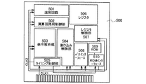
500 マイクロプロセッサ
501 演算回路
502 演算回路制御部
503 命令解析部
504 制御部
505 タイミング制御部
506 レジスタ
507 レジスタ制御部
508 バスインターフェース
509 専用メモリ
510 メモリインターフェース
511 RFCPU
512 アナログ回路部
513 デジタル回路部
514 共振回路
515 整流回路
516 定電圧回路
517 リセット回路
518 発振回路
519 復調回路
520 変調回路
521 RFインターフェース
522 制御レジスタ
523 クロックコントローラ
524 CPUインターフェース
525 中央処理ユニット
526 ランダムアクセスメモリ
527 専用メモリ
528 アンテナ
529 容量部
530 電源管理回路
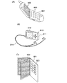
901 携帯電話機
902 表示部
903 操作スイッチ
911 デジタルプレーヤー
912 表示部
913 操作部
914 イヤホン
921 電子ブック
922 表示部
923 操作スイッチ
Claims (13)
- 表面に接合層が形成され、所定の深さに剥離層が形成された半導体基板と、歪点が700℃以下のベース基板とを用意し、
前記半導体基板の表面と前記ベース基板の表面とを対向させ、前記接合層の表面と前記ベース基板とを接合し、
熱処理を行うことにより前記接合層を境として前記半導体基板の一部を分離させ、前記ベース基板上に単結晶半導体層を形成する工程を含み、
前記ベース基板として、前記熱処理により等方的に収縮する基板を用いることを特徴とするSOI基板の作製方法。 - 表面に絶縁層が形成され、前記絶縁層上に接合層が形成され、所定の深さに剥離層が形成された半導体基板と、歪点が700℃以下のベース基板とを用意し、
前記半導体基板の表面と前記ベース基板の表面とを対向させ、前記接合層の表面と前記ベース基板とを接合し、
熱処理を行うことにより前記接合層を境として前記半導体基板の一部を分離させ、前記ベース基板上に単結晶半導体層を形成する工程を含み、
前記ベース基板として、前記熱処理により等方的に収縮する基板を用いることを特徴とするSOI基板の作製方法。 - 請求項2において、
前記絶縁層として、有機シランガスを用いて化学気相成長法により形成される酸化シリコン膜を用いることを特徴とするSOI基板の作製方法。 - 請求項1乃至請求項3のいずれか一項において、
前記接合層として、窒素含有層を用いることを特徴とするSOI基板の作製方法。 - 表面に接合層が形成され、所定の深さに剥離層が形成された半導体基板と、表面に絶縁層が形成され歪点が700℃以下のベース基板とを用意し、
前記半導体基板の表面と前記ベース基板の表面とを対向させ、前記接合層の表面と前記絶縁層の表面とを接合し、
熱処理を行うことにより前記接合層を境として前記半導体基板の一部を分離させ、前記ベース基板上に単結晶半導体層を形成する工程を含み、
前記ベース基板として、前記熱処理により等方的に収縮する基板を用いることを特徴とするSOI基板の作製方法。 - 請求項5において、
前記接合層として、有機シランガスを用いて化学気相成長法により形成される酸化シリコン膜を用い、
前記絶縁層として、窒素含有層を用いることを特徴とするSOI基板の作製方法。 - 請求項1乃至請求項6のいずれか一項において、
前記熱処理を、400℃以上700℃以下で行うことを特徴とするSOI基板の作製方法。 - 請求項1乃至請求項7のいずれか一項において、
前記ベース基板として、前記半導体基板と熱膨張係数が同等又は前記半導体基板より熱膨張係数が大きい基板を用いることを特徴とするSOI基板の作製方法。 - 請求項8において、
前記ベース基板の熱膨張係数を、前記半導体基板の熱膨張係数の0.85倍〜2.0倍とすることを特徴とするSOI基板の作製方法。 - 請求項8において、
前記半導体基板としてシリコン基板を用い、
前記ベース基板として熱膨張係数が、2.3×10⁻⁶〜5.0×10⁻⁶/℃である基板を用いることを特徴とするSOI基板の作製方法。 - 請求項1乃至請求項10のいずれか一項において、
前記ベース基板として、ガラス基板を用いることを特徴とするSOI基板の作製方法。 - 請求項11において、
前記ガラス基板として、表面が研磨されたものを用いることを特徴とするSOI基板の作製方法。 - 請求項11又は請求項12において、
前記ガラス基板として、表面粗さが0.3nm以下のものを用いることを特徴とするSOI基板の作製方法。
Priority Applications (1)
| Application Number | Priority Date | Filing Date | Title |
|---|---|---|---|
| JP2008261507A JP2009111373A (ja) | 2007-10-10 | 2008-10-08 | Soi基板の作製方法 |
Applications Claiming Priority (2)
| Application Number | Priority Date | Filing Date | Title |
|---|---|---|---|
| JP2007264983 | 2007-10-10 | ||
| JP2008261507A JP2009111373A (ja) | 2007-10-10 | 2008-10-08 | Soi基板の作製方法 |
Publications (2)
| Publication Number | Publication Date |
|---|---|
| JP2009111373A true JP2009111373A (ja) | 2009-05-21 |
| JP2009111373A5 JP2009111373A5 (ja) | 2011-10-27 |
Family
ID=40534669
Family Applications (1)
| Application Number | Title | Priority Date | Filing Date |
|---|---|---|---|
| JP2008261507A Withdrawn JP2009111373A (ja) | 2007-10-10 | 2008-10-08 | Soi基板の作製方法 |
Country Status (3)
| Country | Link |
|---|---|
| US (1) | US8236668B2 (ja) |
| JP (1) | JP2009111373A (ja) |
| KR (1) | KR101561855B1 (ja) |
Cited By (4)
| Publication number | Priority date | Publication date | Assignee | Title |
|---|---|---|---|---|
| JP2012054539A (ja) * | 2010-08-05 | 2012-03-15 | Semiconductor Energy Lab Co Ltd | 半導体装置の作製方法 |
| JP2013008968A (ja) * | 2011-06-23 | 2013-01-10 | Soytec | 一時的接着を利用して半導体構造を製造するためのプロセス |
| WO2014200827A1 (en) * | 2013-06-13 | 2014-12-18 | Yan Ye | Methods and apparatuses for delaminating process pieces |
| WO2016039541A1 (ko) * | 2014-09-12 | 2016-03-17 | 한양대학교 산학협력단 | 전자 소자, 및 그 제조 방법 |
Families Citing this family (17)
| Publication number | Priority date | Publication date | Assignee | Title |
|---|---|---|---|---|
| US7348227B1 (en) * | 1995-03-23 | 2008-03-25 | Semiconductor Energy Laboratory Co., Ltd. | Semiconductor device and manufacturing method thereof |
| EP2143146A1 (en) * | 2007-04-13 | 2010-01-13 | Semiconductor Energy Laboratory Co, Ltd. | Photovoltaic device and method for manufacturing the same |
| JP5654206B2 (ja) * | 2008-03-26 | 2015-01-14 | 株式会社半導体エネルギー研究所 | Soi基板の作製方法及び該soi基板を用いた半導体装置 |
| JP5548395B2 (ja) * | 2008-06-25 | 2014-07-16 | 株式会社半導体エネルギー研究所 | Soi基板の作製方法 |
| WO2010109712A1 (ja) * | 2009-03-25 | 2010-09-30 | シャープ株式会社 | 半導体装置用の絶縁基板、及び、半導体装置 |
| WO2011111505A1 (en) * | 2010-03-08 | 2011-09-15 | Semiconductor Energy Laboratory Co., Ltd. | Semiconductor device and method for manufacturing semiconductor device |
| KR101144840B1 (ko) * | 2010-06-08 | 2012-05-14 | 삼성코닝정밀소재 주식회사 | 접합기판 제조방법 |
| KR101144842B1 (ko) * | 2010-06-08 | 2012-05-14 | 삼성코닝정밀소재 주식회사 | 접합기판 제조방법 |
| JP5917036B2 (ja) | 2010-08-05 | 2016-05-11 | 株式会社半導体エネルギー研究所 | Soi基板の作製方法 |
| US8735263B2 (en) | 2011-01-21 | 2014-05-27 | Semiconductor Energy Laboratory Co., Ltd. | Method for manufacturing SOI substrate |
| CN103155102A (zh) * | 2011-02-15 | 2013-06-12 | 住友电气工业株式会社 | 具有保护膜的复合衬底和制造半导体器件的方法 |
| US8497185B2 (en) * | 2011-03-07 | 2013-07-30 | Sumitomo Electric Industries, Ltd. | Method of manufacturing semiconductor wafer, and composite base and composite substrate for use in that method |
| US9184228B2 (en) | 2011-03-07 | 2015-11-10 | Sumitomo Electric Industries, Ltd. | Composite base including sintered base and base surface flattening layer, and composite substrate including that composite base and semiconductor crystalline layer |
| US9711744B2 (en) | 2012-12-21 | 2017-07-18 | 3M Innovative Properties Company | Patterned structured transfer tape |
| US20150202834A1 (en) | 2014-01-20 | 2015-07-23 | 3M Innovative Properties Company | Lamination transfer films for forming antireflective structures |
| WO2016064565A1 (en) | 2014-10-20 | 2016-04-28 | 3M Innovative Properties Company | Insulated glazing units and microoptical layer comprising microstructured diffuser and methods |
| US11908723B2 (en) * | 2021-12-03 | 2024-02-20 | International Business Machines Corporation | Silicon handler with laser-release layers |
Citations (5)
| Publication number | Priority date | Publication date | Assignee | Title |
|---|---|---|---|---|
| JP2002170942A (ja) * | 2000-11-30 | 2002-06-14 | Seiko Epson Corp | Soi基板、素子基板、電気光学装置及び電子機器、並びにsoi基板の製造方法、素子基板の製造方法 |
| JP2002261290A (ja) * | 2001-03-01 | 2002-09-13 | Sony Corp | 半導体薄膜の形成方法及びそれを用いた薄膜トランジスタの製造方法 |
| JP2004087606A (ja) * | 2002-08-23 | 2004-03-18 | Sharp Corp | Soi基板およびそれを用いる表示装置ならびにsoi基板の製造方法 |
| JP2005285850A (ja) * | 2004-03-26 | 2005-10-13 | Sharp Corp | 半導体基板、半導体装置、及びそれらの製造方法 |
| JP2008294417A (ja) * | 2007-04-27 | 2008-12-04 | Semiconductor Energy Lab Co Ltd | 半導体基板の作製方法、及び半導体装置の作製方法 |
Family Cites Families (82)
| Publication number | Priority date | Publication date | Assignee | Title |
|---|---|---|---|---|
| US5528397A (en) | 1991-12-03 | 1996-06-18 | Kopin Corporation | Single crystal silicon transistors for display panels |
| FR2681472B1 (fr) | 1991-09-18 | 1993-10-29 | Commissariat Energie Atomique | Procede de fabrication de films minces de materiau semiconducteur. |
| JP3237888B2 (ja) | 1992-01-31 | 2001-12-10 | キヤノン株式会社 | 半導体基体及びその作製方法 |
| JP2742747B2 (ja) | 1992-05-29 | 1998-04-22 | 株式会社半導体エネルギー研究所 | 薄膜トランジスタを有する多層半導体集積回路 |
| TW264575B (ja) | 1993-10-29 | 1995-12-01 | Handotai Energy Kenkyusho Kk | |
| US5923962A (en) | 1993-10-29 | 1999-07-13 | Semiconductor Energy Laboratory Co., Ltd. | Method for manufacturing a semiconductor device |
| JP3431033B2 (ja) | 1993-10-29 | 2003-07-28 | 株式会社半導体エネルギー研究所 | 半導体作製方法 |
| JP3067949B2 (ja) | 1994-06-15 | 2000-07-24 | シャープ株式会社 | 電子装置および液晶表示装置 |
| FR2748851B1 (fr) | 1996-05-15 | 1998-08-07 | Commissariat Energie Atomique | Procede de realisation d'une couche mince de materiau semiconducteur |
| JP4103968B2 (ja) | 1996-09-18 | 2008-06-18 | 株式会社半導体エネルギー研究所 | 絶縁ゲイト型半導体装置 |
| JPH10284431A (ja) | 1997-04-11 | 1998-10-23 | Sharp Corp | Soi基板の製造方法 |
| US6191007B1 (en) | 1997-04-28 | 2001-02-20 | Denso Corporation | Method for manufacturing a semiconductor substrate |
| JPH1197379A (ja) | 1997-07-25 | 1999-04-09 | Denso Corp | 半導体基板及び半導体基板の製造方法 |
| US6534380B1 (en) | 1997-07-18 | 2003-03-18 | Denso Corporation | Semiconductor substrate and method of manufacturing the same |
| US6388652B1 (en) | 1997-08-20 | 2002-05-14 | Semiconductor Energy Laboratory Co., Ltd. | Electrooptical device |
| JP3324469B2 (ja) | 1997-09-26 | 2002-09-17 | 信越半導体株式会社 | Soiウエーハの製造方法ならびにこの方法で製造されるsoiウエーハ |
| US6686623B2 (en) | 1997-11-18 | 2004-02-03 | Semiconductor Energy Laboratory Co., Ltd. | Nonvolatile memory and electronic apparatus |
| JP2000012864A (ja) | 1998-06-22 | 2000-01-14 | Semiconductor Energy Lab Co Ltd | 半導体装置の作製方法 |
| US6271101B1 (en) | 1998-07-29 | 2001-08-07 | Semiconductor Energy Laboratory Co., Ltd. | Process for production of SOI substrate and process for production of semiconductor device |
| JP4476390B2 (ja) | 1998-09-04 | 2010-06-09 | 株式会社半導体エネルギー研究所 | 半導体装置の作製方法 |
| JP2000124092A (ja) | 1998-10-16 | 2000-04-28 | Shin Etsu Handotai Co Ltd | 水素イオン注入剥離法によってsoiウエーハを製造する方法およびこの方法で製造されたsoiウエーハ |
| US6287941B1 (en) | 1999-04-21 | 2001-09-11 | Silicon Genesis Corporation | Surface finishing of SOI substrates using an EPI process |
| JP4101409B2 (ja) | 1999-08-19 | 2008-06-18 | シャープ株式会社 | 半導体装置の製造方法 |
| US6261957B1 (en) | 1999-08-20 | 2001-07-17 | Taiwan Semiconductor Manufacturing Company | Self-planarized gap-filling by HDPCVD for shallow trench isolation |
| US6653209B1 (en) | 1999-09-30 | 2003-11-25 | Canon Kabushiki Kaisha | Method of producing silicon thin film, method of constructing SOI substrate and semiconductor device |
| WO2001042820A2 (en) | 1999-12-02 | 2001-06-14 | Teraconnect, Inc. | Method of making optoelectronic devices using sacrificial devices |
| US6525415B2 (en) | 1999-12-28 | 2003-02-25 | Fuji Xerox Co., Ltd. | Three-dimensional semiconductor integrated circuit apparatus and manufacturing method therefor |
| US20010053559A1 (en) | 2000-01-25 | 2001-12-20 | Semiconductor Energy Laboratory Co., Ltd. | Method of fabricating display device |
| US6475072B1 (en) | 2000-09-29 | 2002-11-05 | International Business Machines Corporation | Method of wafer smoothing for bonding using chemo-mechanical polishing (CMP) |
| FR2894990B1 (fr) | 2005-12-21 | 2008-02-22 | Soitec Silicon On Insulator | Procede de fabrication de substrats, notamment pour l'optique,l'electronique ou l'optoelectronique et substrat obtenu selon ledit procede |
| JP4803884B2 (ja) | 2001-01-31 | 2011-10-26 | キヤノン株式会社 | 薄膜半導体装置の製造方法 |
| US7253032B2 (en) | 2001-04-20 | 2007-08-07 | Semiconductor Energy Laboratory Co., Ltd. | Method of flattening a crystallized semiconductor film surface by using a plate |
| TW544938B (en) | 2001-06-01 | 2003-08-01 | Semiconductor Energy Lab | Method of manufacturing a semiconductor device |
| TW548860B (en) | 2001-06-20 | 2003-08-21 | Semiconductor Energy Lab | Light emitting device and method of manufacturing the same |
| TW594947B (en) | 2001-10-30 | 2004-06-21 | Semiconductor Energy Lab | Semiconductor device and method of manufacturing the same |
| JP4182323B2 (ja) | 2002-02-27 | 2008-11-19 | ソニー株式会社 | 複合基板、基板製造方法 |
| US7119365B2 (en) | 2002-03-26 | 2006-10-10 | Sharp Kabushiki Kaisha | Semiconductor device and manufacturing method thereof, SOI substrate and display device using the same, and manufacturing method of the SOI substrate |
| JP4289837B2 (ja) | 2002-07-15 | 2009-07-01 | アプライド マテリアルズ インコーポレイテッド | イオン注入方法及びsoiウエハの製造方法 |
| JP4328067B2 (ja) | 2002-07-31 | 2009-09-09 | アプライド マテリアルズ インコーポレイテッド | イオン注入方法及びsoiウエハの製造方法、並びにイオン注入装置 |
| KR100511656B1 (ko) | 2002-08-10 | 2005-09-07 | 주식회사 실트론 | 나노 에스오아이 웨이퍼의 제조방법 및 그에 따라 제조된나노 에스오아이 웨이퍼 |
| US6818529B2 (en) | 2002-09-12 | 2004-11-16 | Applied Materials, Inc. | Apparatus and method for forming a silicon film across the surface of a glass substrate |
| US7508034B2 (en) | 2002-09-25 | 2009-03-24 | Sharp Kabushiki Kaisha | Single-crystal silicon substrate, SOI substrate, semiconductor device, display device, and manufacturing method of semiconductor device |
| US6759277B1 (en) | 2003-02-27 | 2004-07-06 | Sharp Laboratories Of America, Inc. | Crystalline silicon die array and method for assembling crystalline silicon sheets onto substrates |
| JP4509488B2 (ja) | 2003-04-02 | 2010-07-21 | 株式会社Sumco | 貼り合わせ基板の製造方法 |
| US7253040B2 (en) | 2003-08-05 | 2007-08-07 | Sharp Kabushiki Kaisha | Fabrication method of semiconductor device |
| EP2259300B1 (en) | 2003-10-28 | 2020-04-08 | Semiconductor Energy Laboratory Co., Ltd. | Manufacture of semiconductor device |
| US6992025B2 (en) | 2004-01-12 | 2006-01-31 | Sharp Laboratories Of America, Inc. | Strained silicon on insulator from film transfer and relaxation by hydrogen implantation |
| JP4759919B2 (ja) | 2004-01-16 | 2011-08-31 | セイコーエプソン株式会社 | 電気光学装置の製造方法 |
| JP5110772B2 (ja) | 2004-02-03 | 2012-12-26 | 株式会社半導体エネルギー研究所 | 半導体薄膜層を有する基板の製造方法 |
| JP2006049800A (ja) | 2004-03-10 | 2006-02-16 | Seiko Epson Corp | 薄膜デバイスの供給体、薄膜デバイスの供給体の製造方法、転写方法、半導体装置の製造方法及び電子機器 |
| JP4407384B2 (ja) | 2004-05-28 | 2010-02-03 | 株式会社Sumco | Soi基板の製造方法 |
| US7560361B2 (en) | 2004-08-12 | 2009-07-14 | International Business Machines Corporation | Method of forming gate stack for semiconductor electronic device |
| US7179719B2 (en) | 2004-09-28 | 2007-02-20 | Sharp Laboratories Of America, Inc. | System and method for hydrogen exfoliation |
| US7410882B2 (en) | 2004-09-28 | 2008-08-12 | Palo Alto Research Center Incorporated | Method of manufacturing and structure of polycrystalline semiconductor thin-film heterostructures on dissimilar substrates |
| US7148124B1 (en) | 2004-11-18 | 2006-12-12 | Alexander Yuri Usenko | Method for forming a fragile layer inside of a single crystalline substrate preferably for making silicon-on-insulator wafers |
| US7193294B2 (en) | 2004-12-03 | 2007-03-20 | Toshiba Ceramics Co., Ltd. | Semiconductor substrate comprising a support substrate which comprises a gettering site |
| KR100601976B1 (ko) | 2004-12-08 | 2006-07-18 | 삼성전자주식회사 | 스트레인 실리콘 온 인슐레이터 구조체 및 그 제조방법 |
| JP4934966B2 (ja) | 2005-02-04 | 2012-05-23 | 株式会社Sumco | Soi基板の製造方法 |
| US7387946B2 (en) | 2005-06-07 | 2008-06-17 | Freescale Semiconductor, Inc. | Method of fabricating a substrate for a planar, double-gated, transistor process |
| KR20080042095A (ko) | 2005-07-27 | 2008-05-14 | 실리콘 제너시스 코포레이션 | 제어된 클리빙 처리를 이용하여 플레이트 상에 다수의 타일영역을 제작하는 방법 및 구조 |
| EP1760798B1 (en) | 2005-08-31 | 2012-01-11 | Semiconductor Energy Laboratory Co., Ltd. | Semiconductor device and manufacturing method thereof |
| KR101299604B1 (ko) | 2005-10-18 | 2013-08-26 | 가부시키가이샤 한도오따이 에네루기 켄큐쇼 | 반도체 장치 및 그 제조 방법 |
| FR2892230B1 (fr) * | 2005-10-19 | 2008-07-04 | Soitec Silicon On Insulator | Traitement d'une couche de germamium |
| US20070117287A1 (en) | 2005-11-23 | 2007-05-24 | Semiconductor Energy Laboratory Co., Ltd. | Laser irradiation apparatus |
| US7579654B2 (en) | 2006-05-31 | 2009-08-25 | Corning Incorporated | Semiconductor on insulator structure made using radiation annealing |
| US20070281440A1 (en) | 2006-05-31 | 2007-12-06 | Jeffrey Scott Cites | Producing SOI structure using ion shower |
| CN101281912B (zh) | 2007-04-03 | 2013-01-23 | 株式会社半导体能源研究所 | Soi衬底及其制造方法以及半导体装置 |
| EP2140480A4 (en) | 2007-04-20 | 2015-04-22 | Semiconductor Energy Lab | METHOD FOR PRODUCING AN SOI SUBSTRATE AND SEMICONDUCTOR ARRANGEMENT |
| KR101440930B1 (ko) | 2007-04-20 | 2014-09-15 | 가부시키가이샤 한도오따이 에네루기 켄큐쇼 | Soi 기판의 제작방법 |
| EP1986230A2 (en) | 2007-04-25 | 2008-10-29 | Semiconductor Energy Laboratory Co., Ltd. | Method of manufacturing SOI substrate and method of manufacturing semiconductor device |
| EP1993128A3 (en) | 2007-05-17 | 2010-03-24 | Semiconductor Energy Laboratory Co., Ltd. | Method for manufacturing soi substrate |
| KR101457656B1 (ko) | 2007-05-17 | 2014-11-04 | 가부시키가이샤 한도오따이 에네루기 켄큐쇼 | 반도체장치의 제조방법, 표시장치의 제조방법, 반도체장치,표시장치 및 전자기기 |
| US7960262B2 (en) | 2007-05-18 | 2011-06-14 | Semiconductor Energy Laboratory Co., Ltd. | Method for manufacturing semiconductor device by applying laser beam to single-crystal semiconductor layer and non-single-crystal semiconductor layer through cap film |
| EP1993127B1 (en) | 2007-05-18 | 2013-04-24 | Semiconductor Energy Laboratory Co., Ltd. | Manufacturing method of SOI substrate |
| US7745268B2 (en) | 2007-06-01 | 2010-06-29 | Semiconductor Energy Laboratory Co., Ltd. | Method for manufacturing a semiconductor device with irradiation of single crystal semiconductor layer in an inert atmosphere |
| WO2008156040A1 (en) | 2007-06-20 | 2008-12-24 | Semiconductor Energy Laboratory Co., Ltd. | Method of manufacturing semiconductor device |
| US7763502B2 (en) * | 2007-06-22 | 2010-07-27 | Semiconductor Energy Laboratory Co., Ltd | Semiconductor substrate, method for manufacturing semiconductor substrate, semiconductor device, and electronic device |
| US7795111B2 (en) | 2007-06-27 | 2010-09-14 | Semiconductor Energy Laboratory Co., Ltd. | Manufacturing method of SOI substrate and manufacturing method of semiconductor device |
| WO2009001836A1 (en) | 2007-06-28 | 2008-12-31 | Semiconductor Energy Laboratory Co., Ltd. | Manufacturing method of semiconductor device |
| JP5507063B2 (ja) | 2007-07-09 | 2014-05-28 | 株式会社半導体エネルギー研究所 | 半導体装置の作製方法 |
| JP5367330B2 (ja) | 2007-09-14 | 2013-12-11 | 株式会社半導体エネルギー研究所 | Soi基板の作製方法及び半導体装置の作製方法 |
| TWI437696B (zh) | 2007-09-21 | 2014-05-11 | Semiconductor Energy Lab | 半導體裝置及其製造方法 |
-
2008
- 2008-10-02 US US12/244,414 patent/US8236668B2/en not_active Expired - Fee Related
- 2008-10-08 JP JP2008261507A patent/JP2009111373A/ja not_active Withdrawn
- 2008-10-10 KR KR1020080099859A patent/KR101561855B1/ko not_active IP Right Cessation
Patent Citations (5)
| Publication number | Priority date | Publication date | Assignee | Title |
|---|---|---|---|---|
| JP2002170942A (ja) * | 2000-11-30 | 2002-06-14 | Seiko Epson Corp | Soi基板、素子基板、電気光学装置及び電子機器、並びにsoi基板の製造方法、素子基板の製造方法 |
| JP2002261290A (ja) * | 2001-03-01 | 2002-09-13 | Sony Corp | 半導体薄膜の形成方法及びそれを用いた薄膜トランジスタの製造方法 |
| JP2004087606A (ja) * | 2002-08-23 | 2004-03-18 | Sharp Corp | Soi基板およびそれを用いる表示装置ならびにsoi基板の製造方法 |
| JP2005285850A (ja) * | 2004-03-26 | 2005-10-13 | Sharp Corp | 半導体基板、半導体装置、及びそれらの製造方法 |
| JP2008294417A (ja) * | 2007-04-27 | 2008-12-04 | Semiconductor Energy Lab Co Ltd | 半導体基板の作製方法、及び半導体装置の作製方法 |
Cited By (6)
| Publication number | Priority date | Publication date | Assignee | Title |
|---|---|---|---|---|
| JP2012054539A (ja) * | 2010-08-05 | 2012-03-15 | Semiconductor Energy Lab Co Ltd | 半導体装置の作製方法 |
| JP2013008968A (ja) * | 2011-06-23 | 2013-01-10 | Soytec | 一時的接着を利用して半導体構造を製造するためのプロセス |
| US8951887B2 (en) | 2011-06-23 | 2015-02-10 | Soitec | Process for fabricating a semiconductor structure employing a temporary bond |
| WO2014200827A1 (en) * | 2013-06-13 | 2014-12-18 | Yan Ye | Methods and apparatuses for delaminating process pieces |
| US9624597B2 (en) | 2013-06-13 | 2017-04-18 | Yan Ye | Methods and apparatuses for delaminating process pieces |
| WO2016039541A1 (ko) * | 2014-09-12 | 2016-03-17 | 한양대학교 산학협력단 | 전자 소자, 및 그 제조 방법 |
Also Published As
| Publication number | Publication date |
|---|---|
| KR20090037363A (ko) | 2009-04-15 |
| US8236668B2 (en) | 2012-08-07 |
| KR101561855B1 (ko) | 2015-10-20 |
| US20090098739A1 (en) | 2009-04-16 |
Similar Documents
| Publication | Publication Date | Title |
|---|---|---|
| KR101561855B1 (ko) | Soi기판의 제작방법 | |
| JP5542256B2 (ja) | Soi基板の作製方法 | |
| JP5383098B2 (ja) | 半導体装置の作製方法 | |
| US7767547B2 (en) | Manufacturing method of SOI substrate | |
| JP5478789B2 (ja) | Soi基板の作製方法 | |
| JP5503866B2 (ja) | Soi基板の作製方法 | |
| US20080248629A1 (en) | Method for manufacturing semiconductor substrate | |
| JP2009004749A (ja) | 半導体基板及び半導体装置並びにそれらの製造方法 | |
| US20120164817A1 (en) | Method for manufacturing soi substrate | |
| JP5500798B2 (ja) | Soi基板の作製方法及び半導体装置の作製方法 | |
| JP5386193B2 (ja) | Soi基板の作製方法 | |
| JP5201967B2 (ja) | 半導体基板の作製方法および半導体装置の作製方法 | |
| JP5478916B2 (ja) | Soi基板の作製方法 | |
| US20110183494A1 (en) | Method for manufacturing soi substrate | |
| JP5430109B2 (ja) | Soi基板の作製方法 | |
| JP2010147313A (ja) | Soi基板の作製方法 |
Legal Events
| Date | Code | Title | Description |
|---|---|---|---|
| RD02 | Notification of acceptance of power of attorney |
Free format text: JAPANESE INTERMEDIATE CODE: A7422 Effective date: 20110824 |
|
| A521 | Written amendment |
Free format text: JAPANESE INTERMEDIATE CODE: A523 Effective date: 20110908 |
|
| A621 | Written request for application examination |
Free format text: JAPANESE INTERMEDIATE CODE: A621 Effective date: 20110908 |
|
| A977 | Report on retrieval |
Free format text: JAPANESE INTERMEDIATE CODE: A971007 Effective date: 20130822 |
|
| A131 | Notification of reasons for refusal |
Free format text: JAPANESE INTERMEDIATE CODE: A131 Effective date: 20130827 |
|
| A761 | Written withdrawal of application |
Free format text: JAPANESE INTERMEDIATE CODE: A761 Effective date: 20130923 |