JP2005051200A - メッキ処理された基板支持体 - Google Patents
メッキ処理された基板支持体 Download PDFInfo
- Publication number
- JP2005051200A JP2005051200A JP2004140365A JP2004140365A JP2005051200A JP 2005051200 A JP2005051200 A JP 2005051200A JP 2004140365 A JP2004140365 A JP 2004140365A JP 2004140365 A JP2004140365 A JP 2004140365A JP 2005051200 A JP2005051200 A JP 2005051200A
- Authority
- JP
- Japan
- Prior art keywords
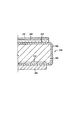
- substrate support
- coating
- substrate
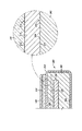
- microinches
- support surface
- Prior art date
- Legal status (The legal status is an assumption and is not a legal conclusion. Google has not performed a legal analysis and makes no representation as to the accuracy of the status listed.)
- Pending
Links
Images


Classifications
-
- H—ELECTRICITY
- H01—ELECTRIC ELEMENTS
- H01J—ELECTRIC DISCHARGE TUBES OR DISCHARGE LAMPS
- H01J37/00—Discharge tubes with provision for introducing objects or material to be exposed to the discharge, e.g. for the purpose of examination or processing thereof
- H01J37/32—Gas-filled discharge tubes
- H01J37/32009—Arrangements for generation of plasma specially adapted for examination or treatment of objects, e.g. plasma sources
- H01J37/32082—Radio frequency generated discharge
-
- C—CHEMISTRY; METALLURGY
- C23—COATING METALLIC MATERIAL; COATING MATERIAL WITH METALLIC MATERIAL; CHEMICAL SURFACE TREATMENT; DIFFUSION TREATMENT OF METALLIC MATERIAL; COATING BY VACUUM EVAPORATION, BY SPUTTERING, BY ION IMPLANTATION OR BY CHEMICAL VAPOUR DEPOSITION, IN GENERAL; INHIBITING CORROSION OF METALLIC MATERIAL OR INCRUSTATION IN GENERAL
- C23C—COATING METALLIC MATERIAL; COATING MATERIAL WITH METALLIC MATERIAL; SURFACE TREATMENT OF METALLIC MATERIAL BY DIFFUSION INTO THE SURFACE, BY CHEMICAL CONVERSION OR SUBSTITUTION; COATING BY VACUUM EVAPORATION, BY SPUTTERING, BY ION IMPLANTATION OR BY CHEMICAL VAPOUR DEPOSITION, IN GENERAL
- C23C16/00—Chemical coating by decomposition of gaseous compounds, without leaving reaction products of surface material in the coating, i.e. chemical vapour deposition [CVD] processes
- C23C16/44—Chemical coating by decomposition of gaseous compounds, without leaving reaction products of surface material in the coating, i.e. chemical vapour deposition [CVD] processes characterised by the method of coating
- C23C16/458—Chemical coating by decomposition of gaseous compounds, without leaving reaction products of surface material in the coating, i.e. chemical vapour deposition [CVD] processes characterised by the method of coating characterised by the method used for supporting substrates in the reaction chamber
- C23C16/4581—Chemical coating by decomposition of gaseous compounds, without leaving reaction products of surface material in the coating, i.e. chemical vapour deposition [CVD] processes characterised by the method of coating characterised by the method used for supporting substrates in the reaction chamber characterised by material of construction or surface finish of the means for supporting the substrate
-
- C—CHEMISTRY; METALLURGY
- C25—ELECTROLYTIC OR ELECTROPHORETIC PROCESSES; APPARATUS THEREFOR
- C25D—PROCESSES FOR THE ELECTROLYTIC OR ELECTROPHORETIC PRODUCTION OF COATINGS; ELECTROFORMING; APPARATUS THEREFOR
- C25D11/00—Electrolytic coating by surface reaction, i.e. forming conversion layers
- C25D11/02—Anodisation
- C25D11/04—Anodisation of aluminium or alloys based thereon
- C25D11/16—Pretreatment, e.g. desmutting
-
- C—CHEMISTRY; METALLURGY
- C25—ELECTROLYTIC OR ELECTROPHORETIC PROCESSES; APPARATUS THEREFOR
- C25D—PROCESSES FOR THE ELECTROLYTIC OR ELECTROPHORETIC PRODUCTION OF COATINGS; ELECTROFORMING; APPARATUS THEREFOR
- C25D11/00—Electrolytic coating by surface reaction, i.e. forming conversion layers
- C25D11/02—Anodisation
- C25D11/04—Anodisation of aluminium or alloys based thereon
- C25D11/18—After-treatment, e.g. pore-sealing
Landscapes
- Chemical & Material Sciences (AREA)
- Engineering & Computer Science (AREA)
- Metallurgy (AREA)
- Chemical Kinetics & Catalysis (AREA)
- Materials Engineering (AREA)
- Organic Chemistry (AREA)
- Electrochemistry (AREA)
- Mechanical Engineering (AREA)
- General Chemical & Material Sciences (AREA)
- Physics & Mathematics (AREA)
- Plasma & Fusion (AREA)
- Analytical Chemistry (AREA)
- Chemical Vapour Deposition (AREA)
- Container, Conveyance, Adherence, Positioning, Of Wafer (AREA)
- Insulated Metal Substrates For Printed Circuits (AREA)
Applications Claiming Priority (1)
| Application Number | Priority Date | Filing Date | Title |
|---|---|---|---|
| US10/435,182 US20040221959A1 (en) | 2003-05-09 | 2003-05-09 | Anodized substrate support |
Related Child Applications (1)
| Application Number | Title | Priority Date | Filing Date |
|---|---|---|---|
| JP2009149983A Division JP2009239300A (ja) | 2003-05-09 | 2009-06-24 | 陽極酸化処理された基板支持体 |
Publications (2)
| Publication Number | Publication Date |
|---|---|
| JP2005051200A true JP2005051200A (ja) | 2005-02-24 |
| JP2005051200A5 JP2005051200A5 (enExample) | 2008-11-06 |
Family
ID=32990571
Family Applications (2)
| Application Number | Title | Priority Date | Filing Date |
|---|---|---|---|
| JP2004140365A Pending JP2005051200A (ja) | 2003-05-09 | 2004-05-10 | メッキ処理された基板支持体 |
| JP2009149983A Pending JP2009239300A (ja) | 2003-05-09 | 2009-06-24 | 陽極酸化処理された基板支持体 |
Family Applications After (1)
| Application Number | Title | Priority Date | Filing Date |
|---|---|---|---|
| JP2009149983A Pending JP2009239300A (ja) | 2003-05-09 | 2009-06-24 | 陽極酸化処理された基板支持体 |
Country Status (6)
| Country | Link |
|---|---|
| US (2) | US20040221959A1 (enExample) |
| EP (1) | EP1475460A1 (enExample) |
| JP (2) | JP2005051200A (enExample) |
| KR (2) | KR20040096785A (enExample) |
| CN (1) | CN100385640C (enExample) |
| TW (1) | TW200507157A (enExample) |
Cited By (3)
| Publication number | Priority date | Publication date | Assignee | Title |
|---|---|---|---|---|
| JP2007051367A (ja) * | 2005-07-15 | 2007-03-01 | Applied Materials Inc | サセプタの粗面化による静電荷の削減 |
| JP2008138283A (ja) * | 2006-12-01 | 2008-06-19 | Applied Materials Inc | 表面テクスチャリングを組み込んだプラズマリアクタ基板 |
| US8372205B2 (en) | 2003-05-09 | 2013-02-12 | Applied Materials, Inc. | Reducing electrostatic charge by roughening the susceptor |
Families Citing this family (33)
| Publication number | Priority date | Publication date | Assignee | Title |
|---|---|---|---|---|
| US20040221959A1 (en) * | 2003-05-09 | 2004-11-11 | Applied Materials, Inc. | Anodized substrate support |
| JP2005064284A (ja) * | 2003-08-14 | 2005-03-10 | Asm Japan Kk | 半導体基板保持装置 |
| TWI287279B (en) * | 2004-09-20 | 2007-09-21 | Applied Materials Inc | Diffuser gravity support |
| US7732056B2 (en) * | 2005-01-18 | 2010-06-08 | Applied Materials, Inc. | Corrosion-resistant aluminum component having multi-layer coating |
| US8173228B2 (en) * | 2006-01-27 | 2012-05-08 | Applied Materials, Inc. | Particle reduction on surfaces of chemical vapor deposition processing apparatus |
| US20070202636A1 (en) * | 2006-02-22 | 2007-08-30 | Applied Materials, Inc. | Method of controlling the film thickness uniformity of PECVD-deposited silicon-comprising thin films |
| KR100812047B1 (ko) * | 2006-08-14 | 2008-03-10 | 삼성에스디아이 주식회사 | 기판 구동부 및 이를 이용한 기판 이동 방법 |
| US7959735B2 (en) * | 2007-02-08 | 2011-06-14 | Applied Materials, Inc. | Susceptor with insulative inserts |
| US7964430B2 (en) * | 2007-05-23 | 2011-06-21 | Applied Materials, Inc. | Silicon layer on a laser transparent conductive oxide layer suitable for use in solar cell applications |
| US20080289686A1 (en) * | 2007-05-23 | 2008-11-27 | Tae Kyung Won | Method and apparatus for depositing a silicon layer on a transmitting conductive oxide layer suitable for use in solar cell applications |
| FR2922899B1 (fr) * | 2007-10-26 | 2010-11-26 | Univ Toulouse | Procede de fabrication d'une structure poreuse ordonnee a partir d'un substrat d'aluminium |
| US9917001B2 (en) * | 2008-01-21 | 2018-03-13 | Applied Materials, Inc. | High temperature fine grain aluminum heater |
| JP5745394B2 (ja) * | 2008-03-20 | 2015-07-08 | アプライド マテリアルズ インコーポレイテッドApplied Materials,Incorporated | 基板支持体、プラズマ反応装置、および、サセプターを形成する方法 |
| US20100000684A1 (en) * | 2008-07-03 | 2010-01-07 | Jong Yong Choi | Dry etching apparatus |
| KR20110084877A (ko) * | 2008-10-16 | 2011-07-26 | 어플라이드 머티어리얼스, 인코포레이티드 | 텍스쳐 처리된 플래튼 |
| US10392718B2 (en) | 2009-09-04 | 2019-08-27 | Apple Inc. | Anodization and polish surface treatment |
| CN107731648B (zh) * | 2010-10-28 | 2020-02-14 | 应用材料公司 | 高纯度铝涂层硬阳极化 |
| JP2012222287A (ja) * | 2011-04-13 | 2012-11-12 | Shimadzu Corp | プラズマcvd成膜装置および基板搭載装置 |
| CN104508180A (zh) * | 2012-07-27 | 2015-04-08 | 应用材料公司 | 粗糙化的基板支撑件 |
| JP6539582B2 (ja) * | 2012-10-01 | 2019-07-03 | フォースト・フィジックス・リミテッド・ライアビリティ・カンパニーForced Physics LLC | 温度制御のためのシステムおよび方法 |
| KR20150129660A (ko) | 2013-03-14 | 2015-11-20 | 어플라이드 머티어리얼스, 인코포레이티드 | 기판 상의 고순도 알루미늄 탑 코트 |
| US9624593B2 (en) | 2013-08-29 | 2017-04-18 | Applied Materials, Inc. | Anodization architecture for electro-plate adhesion |
| US9663870B2 (en) * | 2013-11-13 | 2017-05-30 | Applied Materials, Inc. | High purity metallic top coat for semiconductor manufacturing components |
| US9975320B2 (en) * | 2014-01-13 | 2018-05-22 | Applied Materials, Inc. | Diffusion bonded plasma resisted chemical vapor deposition (CVD) chamber heater |
| CN103956349B (zh) * | 2014-05-20 | 2016-06-15 | 株洲南车时代电气股份有限公司 | 功率半导体芯片的铜金属化结构及其制作方法 |
| JP6170029B2 (ja) * | 2014-11-07 | 2017-07-26 | トヨタ自動車株式会社 | 遮熱膜の形成方法 |
| KR102632725B1 (ko) | 2016-03-17 | 2024-02-05 | 에이에스엠 아이피 홀딩 비.브이. | 기판 지지 플레이트 및 이를 포함하는 박막 증착 장치 및 박막 증착 방법 |
| CN107201507B (zh) * | 2016-03-17 | 2019-09-17 | Asm知识产权私人控股有限公司 | 衬底支撑板和包含其的薄膜沉积设备 |
| KR102652258B1 (ko) * | 2016-07-12 | 2024-03-28 | 에이비엠 주식회사 | 금속부품 및 그 제조 방법 및 금속부품을 구비한 공정챔버 |
| US11330673B2 (en) | 2017-11-20 | 2022-05-10 | Applied Materials, Inc. | Heated substrate support |
| US10914114B2 (en) * | 2018-07-06 | 2021-02-09 | Guardian Glass, LLC | Electric potentially-driven shade including shutter supporting surface-modified conductive coating, and/or method of making the same |
| CN109881184B (zh) * | 2019-03-29 | 2022-03-25 | 拓荆科技股份有限公司 | 具有静电力抑制的基板承载装置 |
| US11521834B2 (en) * | 2020-08-26 | 2022-12-06 | Tokyo Electron Limited | Plasma processing systems and methods for chemical processing a substrate |
Family Cites Families (96)
| Publication number | Priority date | Publication date | Assignee | Title |
|---|---|---|---|---|
| US3019522A (en) * | 1958-06-23 | 1962-02-06 | John M Bluth | Reformation of metallic surfaces |
| US3616310A (en) * | 1969-03-10 | 1971-10-26 | Kaiser Aluminium Chem Corp | Aluminum-anodizing process |
| JPS59117675U (ja) * | 1983-01-24 | 1984-08-08 | 旭可鍛鉄株式会社 | アルミニウム又はその合金における陽極酸化皮膜の構造 |
| US4801785A (en) * | 1986-01-14 | 1989-01-31 | Raychem Corporation | Electrical devices |
| US5200157A (en) * | 1986-02-17 | 1993-04-06 | Toshiba Ceramics Co., Ltd. | Susceptor for vapor-growth deposition |
| DE3714517A1 (de) * | 1987-04-30 | 1988-11-17 | Oberdorfer Fa F | Fadentrenner fuer nahtmaschinen, insbesondere zum nahten von entwaesserungssieben, trockensieben, filzen u. dgl. |
| US4862799A (en) * | 1987-11-13 | 1989-09-05 | Rockwell International Corporation | Copper coated anodized aluminum ink metering roller |
| US5314601A (en) * | 1989-06-30 | 1994-05-24 | Eltech Systems Corporation | Electrodes of improved service life |
| JPH0686662B2 (ja) | 1989-11-02 | 1994-11-02 | イビデン株式会社 | Cvd用サセプター |
| US5104014A (en) * | 1990-06-28 | 1992-04-14 | John F. Flynn | Trapunto rod to stuff quilted items |
| US4974369A (en) * | 1990-06-28 | 1990-12-04 | William Dixon | Two-dimensionally grooved sanding pad |
| JP2748181B2 (ja) * | 1990-07-26 | 1998-05-06 | キヤノン株式会社 | ウエハチャック |
| US5395342A (en) * | 1990-07-26 | 1995-03-07 | Yoon; Inbae | Endoscopic portal |
| SU1797027A1 (ru) | 1990-07-27 | 1993-02-23 | Ni Elektrotekh I | Полупроводниковый датчик состава газов и способ его изготовления |
| US5104514A (en) * | 1991-05-16 | 1992-04-14 | The United States Of America As Represented By The Secretary Of The Navy | Protective coating system for aluminum |
| JP3142619B2 (ja) * | 1991-12-09 | 2001-03-07 | 株式会社設備デザイン建築設備士事務所 | 外装用アルマイト建材の製造方法 |
| US5290424A (en) * | 1992-01-31 | 1994-03-01 | Aluminum Company Of America | Method of making a shaped reflective aluminum strip, doubly-protected with oxide and fluoropolymer coatings |
| US5401319A (en) * | 1992-08-27 | 1995-03-28 | Applied Materials, Inc. | Lid and door for a vacuum chamber and pretreatment therefor |
| US5401573A (en) * | 1992-11-30 | 1995-03-28 | Mcdonnell Douglas Corporation | Protection of thermal control coatings from ultraviolet radiation |
| US5366585A (en) * | 1993-01-28 | 1994-11-22 | Applied Materials, Inc. | Method and apparatus for protection of conductive surfaces in a plasma processing reactor |
| US5384682A (en) * | 1993-03-22 | 1995-01-24 | Toto Ltd. | Electrostatic chuck |
| FR2714234B1 (fr) * | 1993-12-16 | 1996-08-23 | Telemecanique | Système de contrôle d'alimentation d'un moteur asynchrone. |
| US20020148941A1 (en) * | 1994-02-17 | 2002-10-17 | Boris Sorokov | Sputtering method and apparatus for depositing a coating onto substrate |
| US5581874A (en) * | 1994-03-28 | 1996-12-10 | Tokyo Electron Limited | Method of forming a bonding portion |
| JP3176219B2 (ja) | 1994-05-31 | 2001-06-11 | 京セラ株式会社 | 静電チャック |
| EP0693709A1 (en) * | 1994-07-18 | 1996-01-24 | Minnesota Mining And Manufacturing Company | Fluoropolymers and fluorochemical surface active agents for improving the antistatic behaviour of materials and light sensitive material having improved antistatic behaviour |
| US5548470A (en) * | 1994-07-19 | 1996-08-20 | International Business Machines Corporation | Characterization, modeling, and design of an electrostatic chuck with improved wafer temperature uniformity |
| US5756222A (en) * | 1994-08-15 | 1998-05-26 | Applied Materials, Inc. | Corrosion-resistant aluminum article for semiconductor processing equipment |
| US5677253A (en) * | 1995-03-30 | 1997-10-14 | Kyocera Corporation | Wafer holding member |
| US5804253A (en) * | 1995-07-17 | 1998-09-08 | Kanegafuchi Chemical Ind. Co., Ltd. | Method for adhering or sealing |
| US6355554B1 (en) * | 1995-07-20 | 2002-03-12 | Samsung Electronics Co., Ltd. | Methods of forming filled interconnections in microelectronic devices |
| US6077781A (en) * | 1995-11-21 | 2000-06-20 | Applied Materials, Inc. | Single step process for blanket-selective CVD aluminum deposition |
| JPH09168171A (ja) * | 1995-12-14 | 1997-06-24 | Semiconductor Energy Lab Co Ltd | 表示装置及びその表示システム |
| US5844205A (en) * | 1996-04-19 | 1998-12-01 | Applied Komatsu Technology, Inc. | Heated substrate support structure |
| EP0803900A3 (en) * | 1996-04-26 | 1999-12-29 | Applied Materials, Inc. | Surface preparation to enhance the adhesion of a dielectric layer |
| JPH09323234A (ja) | 1996-06-05 | 1997-12-16 | Nippon Cement Co Ltd | 静電チャック及びその製造方法 |
| US5856236A (en) * | 1996-06-14 | 1999-01-05 | Micron Technology, Inc. | Method of depositing a smooth conformal aluminum film on a refractory metal nitride layer |
| US5916454A (en) * | 1996-08-30 | 1999-06-29 | Lam Research Corporation | Methods and apparatus for reducing byproduct particle generation in a plasma processing chamber |
| US6007673A (en) * | 1996-10-02 | 1999-12-28 | Matsushita Electronics Corporation | Apparatus and method of producing an electronic device |
| US6537905B1 (en) * | 1996-12-30 | 2003-03-25 | Applied Materials, Inc. | Fully planarized dual damascene metallization using copper line interconnect and selective CVD aluminum plug |
| US6055927A (en) * | 1997-01-14 | 2000-05-02 | Applied Komatsu Technology, Inc. | Apparatus and method for white powder reduction in silicon nitride deposition using remote plasma source cleaning technology |
| US5858464A (en) * | 1997-02-13 | 1999-01-12 | Applied Materials, Inc. | Methods and apparatus for minimizing excess aluminum accumulation in CVD chambers |
| JP3160229B2 (ja) | 1997-06-06 | 2001-04-25 | 日本エー・エス・エム株式会社 | プラズマcvd装置用サセプタ及びその製造方法 |
| FR2764310B1 (fr) * | 1997-06-10 | 1999-07-09 | Commissariat Energie Atomique | Materiau multicouches a revetement anti-erosion, anti-abrasion, et anti-usure sur substrat en aluminium, en magnesium ou en leurs alliages |
| US6024044A (en) * | 1997-10-09 | 2000-02-15 | Applied Komatsu Technology, Inc. | Dual frequency excitation of plasma for film deposition |
| JP3283459B2 (ja) * | 1997-12-17 | 2002-05-20 | 日本エー・エス・エム株式会社 | 半導体処理用の基板保持装置 |
| US6064031A (en) * | 1998-03-20 | 2000-05-16 | Mcdonnell Douglas Corporation | Selective metal matrix composite reinforcement by laser deposition |
| US6184489B1 (en) * | 1998-04-13 | 2001-02-06 | Nec Corporation | Particle-removing apparatus for a semiconductor device manufacturing apparatus and method of removing particles |
| JP3588253B2 (ja) * | 1998-06-04 | 2004-11-10 | 京セラ株式会社 | 静電チャック |
| US6117772A (en) * | 1998-07-10 | 2000-09-12 | Ball Semiconductor, Inc. | Method and apparatus for blanket aluminum CVD on spherical integrated circuits |
| DE19839997C1 (de) * | 1998-09-02 | 2000-06-21 | Siemens Ag | Elektronische Schaltungsanordnung |
| FR2783970B1 (fr) * | 1998-09-25 | 2000-11-03 | Commissariat Energie Atomique | Dispositif autorisant le traitement d'un substrat dans une machine prevue pour traiter de plus grands substrats et systeme de montage d'un substrat dans ce dispositif |
| US6081874A (en) * | 1998-09-29 | 2000-06-27 | International Business Machines Corporation | Non-uniform memory access (NUMA) data processing system that speculatively issues requests on a node interconnect |
| US6726304B2 (en) * | 1998-10-09 | 2004-04-27 | Eastman Kodak Company | Cleaning and repairing fluid for printhead cleaning |
| JP3438625B2 (ja) * | 1998-12-10 | 2003-08-18 | マックス株式会社 | 鉄筋結束用リール巻きワイヤの緩み防止方法 |
| JP2001209981A (ja) * | 1999-02-09 | 2001-08-03 | Ricoh Co Ltd | 光ディスク基板成膜装置、光ディスク基板成膜方法、基板ホルダーの製造方法、基板ホルダー、光ディスクおよび相変化記録型光ディスク |
| EP1193751B1 (en) | 1999-04-06 | 2006-05-17 | Tokyo Electron Limited | Electrode and method of manufacturing an electrode |
| TW465017B (en) * | 1999-04-13 | 2001-11-21 | Applied Materials Inc | A corrosion-resistant protective coating for an apparatus and method for processing a substrate |
| JP3911902B2 (ja) * | 1999-04-16 | 2007-05-09 | 東京エレクトロン株式会社 | 処理装置及び金属部品の表面処理方法 |
| US6322712B1 (en) * | 1999-09-01 | 2001-11-27 | Micron Technology, Inc. | Buffer layer in flat panel display |
| US6423175B1 (en) * | 1999-10-06 | 2002-07-23 | Taiwan Semiconductor Manufacturing Co., Ltd | Apparatus and method for reducing particle contamination in an etcher |
| US6649031B1 (en) * | 1999-10-08 | 2003-11-18 | Hybrid Power Generation Systems, Llc | Corrosion resistant coated fuel cell bipolar plate with filled-in fine scale porosities and method of making the same |
| US6196001B1 (en) * | 1999-10-12 | 2001-03-06 | Alliedsignal Inc. | Environment controlled WIP cart |
| JP2001117079A (ja) | 1999-10-18 | 2001-04-27 | Ibiden Co Ltd | 液晶表示板用の基板の加熱装置 |
| US6207558B1 (en) * | 1999-10-21 | 2001-03-27 | Applied Materials, Inc. | Barrier applications for aluminum planarization |
| US6775873B2 (en) * | 2000-02-09 | 2004-08-17 | Eugene H. Luoma | Apparatus for removing hair from a drain |
| US6403479B1 (en) | 2000-03-17 | 2002-06-11 | Hitachi, Ltd. | Process for producing semiconductor and apparatus for production |
| JP2001298013A (ja) | 2000-04-13 | 2001-10-26 | Sharp Corp | 基板処理装置 |
| JP2001355072A (ja) * | 2000-06-13 | 2001-12-25 | Anelva Corp | 基板処理装置 |
| SG106588A1 (en) * | 2000-10-10 | 2004-10-29 | Inst Data Storage | Method for producing thin film magnetic devices having increased orientation ratio |
| US6470508B2 (en) * | 2000-11-08 | 2002-10-29 | Watkins Manufacturing Corporation | Air check valve system for a spa |
| US6554907B2 (en) * | 2001-01-02 | 2003-04-29 | Applied Materials, Inc. | Susceptor with internal support |
| TWI272689B (en) | 2001-02-16 | 2007-02-01 | Tokyo Electron Ltd | Method and apparatus for transferring heat from a substrate to a chuck |
| JP3758979B2 (ja) * | 2001-02-27 | 2006-03-22 | 京セラ株式会社 | 静電チャック及び処理装置 |
| JP4359001B2 (ja) * | 2001-03-02 | 2009-11-04 | 本田技研工業株式会社 | 陽極酸化膜改質方法、陽極酸化膜構造及びアルミニウム合金製船外機 |
| US6458683B1 (en) * | 2001-03-30 | 2002-10-01 | Taiwan Semiconductor Manufacturing Co., Ltd | Method for forming aluminum bumps by CVD and wet etch |
| JP2002313781A (ja) | 2001-04-11 | 2002-10-25 | Sumitomo Electric Ind Ltd | 基板処理装置 |
| KR100422446B1 (ko) * | 2001-07-12 | 2004-03-12 | 삼성전자주식회사 | 건식식각장치의 이그저스트링 |
| US20030047464A1 (en) * | 2001-07-27 | 2003-03-13 | Applied Materials, Inc. | Electrochemically roughened aluminum semiconductor processing apparatus surfaces |
| KR100789453B1 (ko) | 2001-07-30 | 2008-01-02 | 엘지.필립스 엘시디 주식회사 | 플라즈마 화학기상증착장비의 프로세스 챔버 |
| US6510888B1 (en) * | 2001-08-01 | 2003-01-28 | Applied Materials, Inc. | Substrate support and method of fabricating the same |
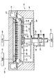
| TW589401B (en) * | 2001-10-24 | 2004-06-01 | Hon Hai Prec Ind Co Ltd | The surface treatment of aluminum article |
| JP3635463B2 (ja) | 2001-11-27 | 2005-04-06 | 東京エレクトロン株式会社 | 自己バイアス測定方法及び装置並びに静電吸着装置 |
| US7048814B2 (en) * | 2002-02-08 | 2006-05-23 | Applied Materials, Inc. | Halogen-resistant, anodized aluminum for use in semiconductor processing apparatus |
| US7033447B2 (en) * | 2002-02-08 | 2006-04-25 | Applied Materials, Inc. | Halogen-resistant, anodized aluminum for use in semiconductor processing apparatus |
| US6776873B1 (en) * | 2002-02-14 | 2004-08-17 | Jennifer Y Sun | Yttrium oxide based surface coating for semiconductor IC processing vacuum chambers |
| US8067067B2 (en) * | 2002-02-14 | 2011-11-29 | Applied Materials, Inc. | Clean, dense yttrium oxide coating protecting semiconductor processing apparatus |
| US6659331B2 (en) * | 2002-02-26 | 2003-12-09 | Applied Materials, Inc | Plasma-resistant, welded aluminum structures for use in semiconductor apparatus |
| US6565984B1 (en) * | 2002-05-28 | 2003-05-20 | Applied Materials Inc. | Clean aluminum alloy for semiconductor processing equipment |
| KR100557882B1 (ko) | 2002-10-10 | 2006-03-10 | 김종균 | 미닫이 문 개폐장치 |
| US6884336B2 (en) * | 2003-01-06 | 2005-04-26 | General Motors Corporation | Color finishing method |
| KR200312050Y1 (ko) | 2003-01-29 | 2003-05-01 | 이기봉 | 차량 시거잭을 이용한 레이저 디텍터 |
| US20040221959A1 (en) | 2003-05-09 | 2004-11-11 | Applied Materials, Inc. | Anodized substrate support |
| US8372205B2 (en) * | 2003-05-09 | 2013-02-12 | Applied Materials, Inc. | Reducing electrostatic charge by roughening the susceptor |
| US7732056B2 (en) * | 2005-01-18 | 2010-06-08 | Applied Materials, Inc. | Corrosion-resistant aluminum component having multi-layer coating |
| KR200432489Y1 (ko) | 2006-09-22 | 2006-12-04 | 김원석 | 논 수위조절장치 |
-
2003
- 2003-05-09 US US10/435,182 patent/US20040221959A1/en not_active Abandoned
-
2004
- 2004-05-06 TW TW093112801A patent/TW200507157A/zh unknown
- 2004-05-08 KR KR1020040032489A patent/KR20040096785A/ko not_active Withdrawn
- 2004-05-09 CN CNB2004100347390A patent/CN100385640C/zh not_active Expired - Lifetime
- 2004-05-10 JP JP2004140365A patent/JP2005051200A/ja active Pending
- 2004-05-10 EP EP04011066A patent/EP1475460A1/en not_active Withdrawn
-
2006
- 2006-04-18 US US11/406,136 patent/US7732010B2/en not_active Expired - Lifetime
- 2006-07-27 KR KR1020060070677A patent/KR20060100302A/ko not_active Ceased
-
2009
- 2009-06-24 JP JP2009149983A patent/JP2009239300A/ja active Pending
Cited By (3)
| Publication number | Priority date | Publication date | Assignee | Title |
|---|---|---|---|---|
| US8372205B2 (en) | 2003-05-09 | 2013-02-12 | Applied Materials, Inc. | Reducing electrostatic charge by roughening the susceptor |
| JP2007051367A (ja) * | 2005-07-15 | 2007-03-01 | Applied Materials Inc | サセプタの粗面化による静電荷の削減 |
| JP2008138283A (ja) * | 2006-12-01 | 2008-06-19 | Applied Materials Inc | 表面テクスチャリングを組み込んだプラズマリアクタ基板 |
Also Published As
| Publication number | Publication date |
|---|---|
| JP2009239300A (ja) | 2009-10-15 |
| TW200507157A (en) | 2005-02-16 |
| US20040221959A1 (en) | 2004-11-11 |
| US7732010B2 (en) | 2010-06-08 |
| KR20040096785A (ko) | 2004-11-17 |
| KR20060100302A (ko) | 2006-09-20 |
| CN100385640C (zh) | 2008-04-30 |
| CN1551326A (zh) | 2004-12-01 |
| US20060185795A1 (en) | 2006-08-24 |
| EP1475460A1 (en) | 2004-11-10 |
Similar Documents
| Publication | Publication Date | Title |
|---|---|---|
| US7732010B2 (en) | Method for supporting a glass substrate to improve uniform deposition thickness | |
| JP2005051200A5 (enExample) | ||
| US8372205B2 (en) | Reducing electrostatic charge by roughening the susceptor | |
| KR100431658B1 (ko) | 기판 가열 장치 및 이를 갖는 장치 | |
| US20020134511A1 (en) | Substrate supporting table,method for producing same, and processing system | |
| EP1928017B1 (en) | Plasma reactor substrate mounting surface texturing | |
| US5626678A (en) | Non-conductive alignment member for uniform plasma processing of substrates | |
| KR101139165B1 (ko) | Ti계 막의 성막 방법 및 기억 매체 | |
| US7815492B2 (en) | Surface treatment method | |
| JPH0830273B2 (ja) | 薄膜形成方法及び装置 | |
| KR101441858B1 (ko) | 서셉터를 러프닝함으로써 정전하를 감소시키는 장치 | |
| JP5745394B2 (ja) | 基板支持体、プラズマ反応装置、および、サセプターを形成する方法 | |
| CN111139458A (zh) | 一种沉积装置 | |
| TW200834688A (en) | Prevention of film deposition on PECVD process chamber wall | |
| JP2523070B2 (ja) | プラズマ処理装置 | |
| JP2951876B2 (ja) | 基板処理方法および基板処理装置 | |
| US20020084036A1 (en) | Susceptor with internal support | |
| JP2005330518A (ja) | プラズマ処理装置 | |
| JP2002110571A (ja) | 成膜装置および成膜方法 | |
| JPH04320031A (ja) | ウエハ加熱用均熱板 | |
| JPH05267277A (ja) | プラズマcvd装置 | |
| WO2007023535A1 (ja) | 成膜方法、成膜用のマスク、および成膜装置 | |
| JP2002134501A (ja) | シリコン酸化膜の成膜方法 |
Legal Events
| Date | Code | Title | Description |
|---|---|---|---|
| A521 | Request for written amendment filed |
Free format text: JAPANESE INTERMEDIATE CODE: A523 Effective date: 20050913 |
|
| A621 | Written request for application examination |
Free format text: JAPANESE INTERMEDIATE CODE: A621 Effective date: 20050913 |
|
| A131 | Notification of reasons for refusal |
Free format text: JAPANESE INTERMEDIATE CODE: A131 Effective date: 20080617 |
|
| A524 | Written submission of copy of amendment under article 19 pct |
Free format text: JAPANESE INTERMEDIATE CODE: A524 Effective date: 20080917 |
|
| A02 | Decision of refusal |
Free format text: JAPANESE INTERMEDIATE CODE: A02 Effective date: 20090224 |