JP2005051200A - Anodized substrate support - Google Patents
Anodized substrate support Download PDFInfo
- Publication number
- JP2005051200A JP2005051200A JP2004140365A JP2004140365A JP2005051200A JP 2005051200 A JP2005051200 A JP 2005051200A JP 2004140365 A JP2004140365 A JP 2004140365A JP 2004140365 A JP2004140365 A JP 2004140365A JP 2005051200 A JP2005051200 A JP 2005051200A
- Authority
- JP
- Japan
- Prior art keywords
- substrate support
- coating
- substrate
- microinches
- support surface
- Prior art date
- Legal status (The legal status is an assumption and is not a legal conclusion. Google has not performed a legal analysis and makes no representation as to the accuracy of the status listed.)
- Pending
Links
- 239000000758 substrate Substances 0.000 title claims abstract description 154
- 238000000576 coating method Methods 0.000 claims abstract description 49
- 239000011248 coating agent Substances 0.000 claims abstract description 47
- 238000000034 method Methods 0.000 claims abstract description 28
- 229910052782 aluminium Inorganic materials 0.000 claims abstract description 26
- XAGFODPZIPBFFR-UHFFFAOYSA-N aluminium Chemical compound [Al] XAGFODPZIPBFFR-UHFFFAOYSA-N 0.000 claims abstract description 26
- 238000010438 heat treatment Methods 0.000 claims description 23
- 239000011324 bead Substances 0.000 claims description 17
- 238000005422 blasting Methods 0.000 claims description 11
- 230000008021 deposition Effects 0.000 claims description 11
- 238000000151 deposition Methods 0.000 claims description 10
- 230000003746 surface roughness Effects 0.000 claims description 8
- 238000005530 etching Methods 0.000 claims description 7
- 238000005270 abrasive blasting Methods 0.000 claims description 6
- 238000004049 embossing Methods 0.000 claims description 6
- 238000000227 grinding Methods 0.000 claims description 6
- TWNQGVIAIRXVLR-UHFFFAOYSA-N oxo(oxoalumanyloxy)alumane Chemical compound O=[Al]O[Al]=O TWNQGVIAIRXVLR-UHFFFAOYSA-N 0.000 claims description 6
- 238000007747 plating Methods 0.000 claims description 4
- 230000003116 impacting effect Effects 0.000 claims description 3
- 230000008878 coupling Effects 0.000 claims description 2
- 238000010168 coupling process Methods 0.000 claims description 2
- 238000005859 coupling reaction Methods 0.000 claims description 2
- 230000002093 peripheral effect Effects 0.000 claims 1
- 239000010408 film Substances 0.000 abstract description 20
- 230000007547 defect Effects 0.000 abstract description 2
- 239000010409 thin film Substances 0.000 abstract description 2
- 239000007789 gas Substances 0.000 description 10
- 238000004519 manufacturing process Methods 0.000 description 10
- 238000000623 plasma-assisted chemical vapour deposition Methods 0.000 description 10
- 230000003014 reinforcing effect Effects 0.000 description 10
- 239000000463 material Substances 0.000 description 9
- 239000011521 glass Substances 0.000 description 8
- 230000008569 process Effects 0.000 description 8
- 238000009826 distribution Methods 0.000 description 6
- 230000032683 aging Effects 0.000 description 5
- 239000000835 fiber Substances 0.000 description 4
- VYPSYNLAJGMNEJ-UHFFFAOYSA-N Silicium dioxide Chemical compound O=[Si]=O VYPSYNLAJGMNEJ-UHFFFAOYSA-N 0.000 description 3
- 239000000919 ceramic Substances 0.000 description 3
- 238000005229 chemical vapour deposition Methods 0.000 description 3
- 239000002243 precursor Substances 0.000 description 3
- 230000009467 reduction Effects 0.000 description 3
- 238000000429 assembly Methods 0.000 description 2
- 230000000712 assembly Effects 0.000 description 2
- 230000015572 biosynthetic process Effects 0.000 description 2
- 230000003750 conditioning effect Effects 0.000 description 2
- 230000001627 detrimental effect Effects 0.000 description 2
- 238000007730 finishing process Methods 0.000 description 2
- 239000004973 liquid crystal related substance Substances 0.000 description 2
- 229910052751 metal Inorganic materials 0.000 description 2
- 239000002184 metal Substances 0.000 description 2
- 238000010926 purge Methods 0.000 description 2
- 230000002787 reinforcement Effects 0.000 description 2
- 239000004065 semiconductor Substances 0.000 description 2
- HBMJWWWQQXIZIP-UHFFFAOYSA-N silicon carbide Chemical compound [Si+]#[C-] HBMJWWWQQXIZIP-UHFFFAOYSA-N 0.000 description 2
- 229910010271 silicon carbide Inorganic materials 0.000 description 2
- RYGMFSIKBFXOCR-UHFFFAOYSA-N Copper Chemical compound [Cu] RYGMFSIKBFXOCR-UHFFFAOYSA-N 0.000 description 1
- UFHFLCQGNIYNRP-UHFFFAOYSA-N Hydrogen Chemical compound [H][H] UFHFLCQGNIYNRP-UHFFFAOYSA-N 0.000 description 1
- 239000004642 Polyimide Substances 0.000 description 1
- 229910052581 Si3N4 Inorganic materials 0.000 description 1
- AZDRQVAHHNSJOQ-UHFFFAOYSA-N alumane Chemical group [AlH3] AZDRQVAHHNSJOQ-UHFFFAOYSA-N 0.000 description 1
- VXAUWWUXCIMFIM-UHFFFAOYSA-M aluminum;oxygen(2-);hydroxide Chemical compound [OH-].[O-2].[Al+3] VXAUWWUXCIMFIM-UHFFFAOYSA-M 0.000 description 1
- 230000008901 benefit Effects 0.000 description 1
- 239000006227 byproduct Substances 0.000 description 1
- 238000005266 casting Methods 0.000 description 1
- 238000006243 chemical reaction Methods 0.000 description 1
- 229910052802 copper Inorganic materials 0.000 description 1
- 239000010949 copper Substances 0.000 description 1
- 239000002178 crystalline material Substances 0.000 description 1
- 238000005137 deposition process Methods 0.000 description 1
- 239000003989 dielectric material Substances 0.000 description 1
- 230000000694 effects Effects 0.000 description 1
- 238000005538 encapsulation Methods 0.000 description 1
- 230000002708 enhancing effect Effects 0.000 description 1
- 239000012530 fluid Substances 0.000 description 1
- 239000001257 hydrogen Substances 0.000 description 1
- 229910052739 hydrogen Inorganic materials 0.000 description 1
- 238000005468 ion implantation Methods 0.000 description 1
- 238000002955 isolation Methods 0.000 description 1
- 239000011159 matrix material Substances 0.000 description 1
- BPUBBGLMJRNUCC-UHFFFAOYSA-N oxygen(2-);tantalum(5+) Chemical compound [O-2].[O-2].[O-2].[O-2].[O-2].[Ta+5].[Ta+5] BPUBBGLMJRNUCC-UHFFFAOYSA-N 0.000 description 1
- 239000002245 particle Substances 0.000 description 1
- 238000005240 physical vapour deposition Methods 0.000 description 1
- 238000007750 plasma spraying Methods 0.000 description 1
- 238000009832 plasma treatment Methods 0.000 description 1
- 229910021420 polycrystalline silicon Inorganic materials 0.000 description 1
- 229920001721 polyimide Polymers 0.000 description 1
- 229920005591 polysilicon Polymers 0.000 description 1
- 239000011253 protective coating Substances 0.000 description 1
- 238000005086 pumping Methods 0.000 description 1
- 230000008439 repair process Effects 0.000 description 1
- 238000000926 separation method Methods 0.000 description 1
- 235000012239 silicon dioxide Nutrition 0.000 description 1
- 239000000377 silicon dioxide Substances 0.000 description 1
- HQVNEWCFYHHQES-UHFFFAOYSA-N silicon nitride Chemical compound N12[Si]34N5[Si]62N3[Si]51N64 HQVNEWCFYHHQES-UHFFFAOYSA-N 0.000 description 1
- 229910052814 silicon oxide Inorganic materials 0.000 description 1
- 238000005507 spraying Methods 0.000 description 1
- 238000004544 sputter deposition Methods 0.000 description 1
- 238000004381 surface treatment Methods 0.000 description 1
- PBCFLUZVCVVTBY-UHFFFAOYSA-N tantalum pentoxide Inorganic materials O=[Ta](=O)O[Ta](=O)=O PBCFLUZVCVVTBY-UHFFFAOYSA-N 0.000 description 1
- 238000007751 thermal spraying Methods 0.000 description 1
- 238000009827 uniform distribution Methods 0.000 description 1
- 235000012431 wafers Nutrition 0.000 description 1
Images


Classifications
-
- H—ELECTRICITY
- H01—ELECTRIC ELEMENTS
- H01J—ELECTRIC DISCHARGE TUBES OR DISCHARGE LAMPS
- H01J37/00—Discharge tubes with provision for introducing objects or material to be exposed to the discharge, e.g. for the purpose of examination or processing thereof
- H01J37/32—Gas-filled discharge tubes
- H01J37/32009—Arrangements for generation of plasma specially adapted for examination or treatment of objects, e.g. plasma sources
- H01J37/32082—Radio frequency generated discharge
-
- C—CHEMISTRY; METALLURGY
- C23—COATING METALLIC MATERIAL; COATING MATERIAL WITH METALLIC MATERIAL; CHEMICAL SURFACE TREATMENT; DIFFUSION TREATMENT OF METALLIC MATERIAL; COATING BY VACUUM EVAPORATION, BY SPUTTERING, BY ION IMPLANTATION OR BY CHEMICAL VAPOUR DEPOSITION, IN GENERAL; INHIBITING CORROSION OF METALLIC MATERIAL OR INCRUSTATION IN GENERAL
- C23C—COATING METALLIC MATERIAL; COATING MATERIAL WITH METALLIC MATERIAL; SURFACE TREATMENT OF METALLIC MATERIAL BY DIFFUSION INTO THE SURFACE, BY CHEMICAL CONVERSION OR SUBSTITUTION; COATING BY VACUUM EVAPORATION, BY SPUTTERING, BY ION IMPLANTATION OR BY CHEMICAL VAPOUR DEPOSITION, IN GENERAL
- C23C16/00—Chemical coating by decomposition of gaseous compounds, without leaving reaction products of surface material in the coating, i.e. chemical vapour deposition [CVD] processes
- C23C16/44—Chemical coating by decomposition of gaseous compounds, without leaving reaction products of surface material in the coating, i.e. chemical vapour deposition [CVD] processes characterised by the method of coating
- C23C16/458—Chemical coating by decomposition of gaseous compounds, without leaving reaction products of surface material in the coating, i.e. chemical vapour deposition [CVD] processes characterised by the method of coating characterised by the method used for supporting substrates in the reaction chamber
- C23C16/4581—Chemical coating by decomposition of gaseous compounds, without leaving reaction products of surface material in the coating, i.e. chemical vapour deposition [CVD] processes characterised by the method of coating characterised by the method used for supporting substrates in the reaction chamber characterised by material of construction or surface finish of the means for supporting the substrate
-
- C—CHEMISTRY; METALLURGY
- C25—ELECTROLYTIC OR ELECTROPHORETIC PROCESSES; APPARATUS THEREFOR
- C25D—PROCESSES FOR THE ELECTROLYTIC OR ELECTROPHORETIC PRODUCTION OF COATINGS; ELECTROFORMING; APPARATUS THEREFOR
- C25D11/00—Electrolytic coating by surface reaction, i.e. forming conversion layers
- C25D11/02—Anodisation
- C25D11/04—Anodisation of aluminium or alloys based thereon
- C25D11/16—Pretreatment, e.g. desmutting
-
- C—CHEMISTRY; METALLURGY
- C25—ELECTROLYTIC OR ELECTROPHORETIC PROCESSES; APPARATUS THEREFOR
- C25D—PROCESSES FOR THE ELECTROLYTIC OR ELECTROPHORETIC PRODUCTION OF COATINGS; ELECTROFORMING; APPARATUS THEREFOR
- C25D11/00—Electrolytic coating by surface reaction, i.e. forming conversion layers
- C25D11/02—Anodisation
- C25D11/04—Anodisation of aluminium or alloys based thereon
- C25D11/18—After-treatment, e.g. pore-sealing
Landscapes
- Chemical & Material Sciences (AREA)
- Engineering & Computer Science (AREA)
- Organic Chemistry (AREA)
- Chemical Kinetics & Catalysis (AREA)
- Materials Engineering (AREA)
- Metallurgy (AREA)
- Electrochemistry (AREA)
- General Chemical & Material Sciences (AREA)
- Mechanical Engineering (AREA)
- Physics & Mathematics (AREA)
- Plasma & Fusion (AREA)
- Analytical Chemistry (AREA)
- Chemical Vapour Deposition (AREA)
- Container, Conveyance, Adherence, Positioning, Of Wafer (AREA)
- Insulated Metal Substrates For Printed Circuits (AREA)
Abstract
Description
発明の分野
[0001]本発明の実施形態は、概して、半導体処理で利用される基板支持体および当該基板支持体を製造する方法を提供する。
Field of Invention
[0001] Embodiments of the present invention generally provide a substrate support for use in semiconductor processing and a method of manufacturing the substrate support.
背景技術の説明
[0002]液晶ディスプレイ又はフラットパネルは、コンピュータ、テレビモニタ、パーソナル・デジタル・アシスタント(PDA)、携帯電話等のようなアクティブマトリックスディスプレイの為に共通して使用される。一般的に、フラットパネルは2つのガラス板を備え、これらに挟まれた液晶層を有する。少なくとも一つのガラス板は、上部に配置される少なくとも一つの導電性膜を含み、これが電源に結合される。電源から導電性膜に供給される電力は、結晶材料の配向性を変更し、当該ディスプレイに見られるテキストやグラフィクスのようなパターンを作り出す。フラットパネルを生産する為に頻繁に使用される、一つの製造方法は、プラズマ増強型化学気相堆積法(PECVD)である。
Background art description
[0002] Liquid crystal displays or flat panels are commonly used for active matrix displays such as computers, television monitors, personal digital assistants (PDAs), cell phones and the like. In general, a flat panel includes two glass plates and has a liquid crystal layer sandwiched between them. The at least one glass plate includes at least one conductive film disposed thereon and is coupled to a power source. The power supplied from the power source to the conductive film changes the orientation of the crystalline material and creates a pattern such as text or graphics found on the display. One manufacturing method frequently used to produce flat panels is plasma enhanced chemical vapor deposition (PECVD).
[0003] プラズマ増強型化学気相堆積法は、フラットパネルや半導体ウエハのような基板上に薄膜を堆積する為に一般的に使用される。プラズマ増強型化学気相堆積法は、基板を含む真空チャンバ内に前駆体ガスを導入することにより一般的に達成される。前駆体ガスは、通常、チャンバの最上部付近に置かれる分配用プレートを通って導かれる。チャンバ内の前駆体ガスは、チャンバに結合された1以上のRF電源からチャンバにRFエネルギを印加することにより、プラズマへと活性化される(励起される)。励起されたガスは、温度制御された基板支持体上に位置決めされた基板の表面上に材料層を形成する為に反応する。低温ポリシリコンの層を基板が受ける適用例において、基板支持体は、400℃を越える温度で加熱される可能性がある。この反応中に生み出される揮発性副産物は、排気システムを介してチャンバから送り出される。 [0003] Plasma enhanced chemical vapor deposition is commonly used to deposit thin films on substrates such as flat panels and semiconductor wafers. Plasma enhanced chemical vapor deposition is generally accomplished by introducing a precursor gas into a vacuum chamber containing the substrate. The precursor gas is typically directed through a distribution plate placed near the top of the chamber. Precursor gas in the chamber is activated (excited) into a plasma by applying RF energy to the chamber from one or more RF power sources coupled to the chamber. The excited gas reacts to form a material layer on the surface of the substrate positioned on the temperature controlled substrate support. In applications where the substrate receives a layer of low temperature polysilicon, the substrate support may be heated at temperatures in excess of 400 ° C. Volatile by-products produced during this reaction are pumped out of the chamber through the exhaust system.
[0004]一般的に、フラットパネル製造に利用される大領域基板は、大きく、しばしば550mm×650mmを越え、表面積では4m2、それを越えるものまで構想されている。対応して、大領域基板を処理する為に利用される基板支持体は、大きな表面領域の基板に適合するように比例して大きくなる。高温使用の為の基板支持体は、一般的に鋳造され、1以上の加熱素子や熱電対がアルミニウム本体内に封入される。基板支持体の大きさのため、1以上の補強部材が一般的に基板支持体内に配置され、高温動作温度(すなわち、膜内の水素含有を最小にするため、350℃を越え500℃に近い温度)における基板支持体の剛性、性能を改善している。アルミニウム製基板支持体は、その後、メッキ処理され、保護被膜を提供する。 [0004] In general, large area substrates utilized in flat panel manufacturing are envisioned to be large, often exceeding 550 mm x 650 mm, with a surface area exceeding 4 m 2 . Correspondingly, the substrate support utilized to process large area substrates is proportionally larger to accommodate large surface area substrates. Substrate supports for high temperature use are typically cast and one or more heating elements or thermocouples are enclosed in an aluminum body. Due to the size of the substrate support, one or more reinforcing members are typically placed within the substrate support and are at high operating temperatures (ie, above 350 ° C. and close to 500 ° C. to minimize hydrogen content in the film). The rigidity and performance of the substrate support in (temperature) is improved. The aluminum substrate support is then plated to provide a protective coating.
[0005]この方法で構成された基板支持体は、良好な処理性能を示すが、しばしば、より薄い膜厚のスポットとして明示されるが、膜厚における小さな局所的変動は、大領域基板上に形成された次世代デバイスにとって有害になる可能性があり、観察されてきた。変動は、基板支持面に沿った、ガラス膜厚と平坦性、通常、約50ミクロインチであるが、ガラス基板を横切る一定の場所で局所的容量変動を作り出し、それにより、堆積変動において生じる局所的なプラズマ非均一性(例えば、堆積された膜厚のスポット)を作り出すと考えられる。 [0005] Substrate supports constructed in this manner exhibit good processing performance, but are often manifested as thinner film thickness spots, but small local variations in film thickness are observed on large area substrates. It can be detrimental to the next generation devices formed and has been observed. The variation is the glass film thickness and flatness along the substrate support surface, usually about 50 microinches, but creates a local capacitance variation at a certain location across the glass substrate, thereby causing local variations in the deposition variation. It is believed to create typical plasma non-uniformities (eg, deposited film thickness spots).
[0006]処理の為に基板をチャンバに移送する前に、特に拡張チャンバ真空パージと組み合わされて実行されるとき、基板支持体のエージング及びプラズマ条件設定の修正により、薄いスポット形成を緩和することが示されてきた。しかし、この方法に必要な時間と材料の、結果として生じる消費や、コストと処理能力における不利な影響は、より効果的な解決策を得ることが望ませるものである。 [0006] Before transferring a substrate to a chamber for processing, particularly when combined with an extended chamber vacuum purge, alleviate thin spot formation by aging the substrate support and modifying plasma condition settings. Has been shown. However, the resulting consumption of time and materials required for this method, and the detrimental effects on cost and throughput, make it desirable to obtain a more effective solution.
[0007]次世代の基板の大きさが大きくなり続けるにつれて、各基板により表わされるフラットパネル製造業者による実質的な投資のため、欠陥減少の重要性は益々重要になっている。さらに、デバイスの継続的な進化と共に、膜の均一性の為の、より密接した許容範囲、膜厚変動の減少及び/又は除去を必要とする危急の寸法減少は、大領域基板上に形成される次世代デバイスの経済的生産にとって重要なファクタになる。 [0007] As the size of next generation substrates continues to grow, the importance of defect reduction becomes more and more important due to the substantial investment by the flat panel manufacturers represented by each substrate. Furthermore, with continued evolution of devices, tighter tolerances for film uniformity, critical dimensional reductions that require reduction and / or removal of film thickness variations are formed on large area substrates. It will be an important factor for the economic production of next-generation devices.
[0008]そのため、改善された基板支持体が必要である。 [0008] Therefore, there is a need for an improved substrate support.
[0009]基板支持体と、当該基板支持体を製造する方法が提供される。本発明の一実施形態において、基板支持体は、電気的絶縁性被膜に覆われた基板支持面を有する電気的導電性本体を含む。基板支持面上の中央に置かれた被膜の少なくとも一部は、約80〜約200ミクロインチの間の表面仕上げを有する。他の実施形態において、基板支持体は、当該本体の一部が上部で基板を支持するように適合され、約80から約200ミクロインチの間の表面仕上げ処理部を有するメッキ処理されたアルミニウム本体を含む。 [0009] A substrate support and a method of manufacturing the substrate support are provided. In one embodiment of the invention, the substrate support includes an electrically conductive body having a substrate support surface covered with an electrically insulating coating. At least a portion of the coating placed centrally on the substrate support surface has a surface finish of between about 80 and about 200 microinches. In other embodiments, the substrate support is a plated aluminum body that is adapted such that a portion of the body supports the substrate on the top and has a surface finish between about 80 and about 200 microinches. including.
[0010]他の実施形態において、基板支持体は、以下の方法により製造される。この方法は、基板支持面で大領域基板を支持するのに適したアルミニウム本体を提供するステップと、約80から約200ミクロインチの間の表面粗さを有するメッキ処理された被膜を基板支持面上に形成するステップと、を含む。 [0010] In another embodiment, the substrate support is manufactured by the following method. The method includes providing an aluminum body suitable for supporting a large area substrate with a substrate support surface, and applying a plated coating having a surface roughness between about 80 and about 200 microinches to the substrate support surface. Forming above.
[0011]簡単に説明された本発明の、より具体的な説明は、添付図面により例示された実施形態を参照される。しかし、添付図面は、本発明の、単なる典型的な実施形態を例示するにすぎず、本発明の範囲を限定するものではなく、本発明は他の効果的な実施形態を許容可能である。 [0011] For a more specific description of the invention briefly described, reference is made to the embodiments illustrated by the accompanying drawings. The accompanying drawings, however, merely illustrate exemplary embodiments of the invention and are not intended to limit the scope of the invention, and the invention is susceptible to other effective embodiments.
[0018]理解を容易にするため、可能な限り、図で共通な同一要素を示すために同一参照符号を使用している。 [0018] To facilitate understanding, identical reference numerals have been used, where possible, to designate identical elements that are common to the figures.
[0019]本発明は、全体的に、大領域基板支持体と、その製造方法を提供する。本発明は、カリフォルニア州サンタクララ市のアプライドマテリアルズ社の一部門であるAKT社から利用可能な、プラズマ増強型化学気相堆積チャンバ(PECVD)のような、プラズマ増強型化学気相堆積チャンバを参照し、以下、例示的に説明する。しかし、本発明は、他のシステム(物理的気相堆積システム、イオン注入システム、エッチングシステム、他の化学気相堆積法および他のシステムであって、内部で基板支持体上の基板を処理することが望まれるもの)でも有用であることが分かる。 [0019] The present invention generally provides large area substrate supports and methods of making the same. The present invention relates to a plasma enhanced chemical vapor deposition chamber, such as a plasma enhanced chemical vapor deposition chamber (PECVD), available from AKT, a division of Applied Materials, Inc. of Santa Clara, California. Reference will be made to the following description. However, the present invention provides other systems (physical vapor deposition systems, ion implantation systems, etching systems, other chemical vapor deposition methods and other systems that internally process a substrate on a substrate support. It is also useful).
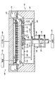
[0020]図1は、一実施形態に係るプラズマ増強型化学気相堆積システム100の横断面図である。当該システム100は、一般的に、ガス源104に結合されたチャンバ102を含む。チャンバ102は、壁106、底部108、リッドアセンブリ110であって、これらは、処理ボリュームを画成する。処理ボリューム112は、通常、壁106内のポート(図示せず)を介してアクセスされ、これが、チャンバ102の内外へ大領域のガラス基板140を移動させることを容易にする。壁106と底部108は、通常、アルミニウム製または処理と両立可能な他の材料であって単一ブロックから製造される。リッドアセンブリ110は、処理ボリューム112を(図示されていない様々なポンプ構成部品に結合された)排気用ポートに結合するポンプ用プレナム114を含む。
[0020] FIG. 1 is a cross-sectional view of a plasma enhanced chemical
[0021]リッドアセンブリ110は、壁106により支持され、チャンバ102を修理するために除去される。リッドアセンブリ110は、一般的にアルミニウムで構成される。分配用プレート118は、リッドアセンブリ110の内側に結合される。分配用プレート118は、通常、アルミニウムから製造される。中央区域は、穿孔領域であり、ここを通って、ガス源104からの処理ガスや他のガスが処理ボリューム112に分配される。分配用プレート118の穿孔領域は、分配用プレート118を通過してチャンバ102内に入るガスの均一な分配を提供するように構成されている。
[0021] The
[0022]加熱された基板支持用アセンブリ138は、チャンバ102内の中央に配置されている。支持用アセンブリ138は、大領域ガラス基板140(以下、「基板140」)を処理中に支持する。基板支持用アセンブリ138は、一般的に、基板140を支持する本体124の少なくとも一部を覆う電気的に絶縁性の被覆180で覆われた電気的に導電性の本体124を含む。被覆180は、約80から約200ミクロインチの表面仕上げ処理部を持ち、これは、高価なエージングや基板支持用アセンブリ138のプラズマ処置を有することなく、堆積の均一性を改善すると証明されてきた。被膜180は、本体124の他の部分を覆ってもよい。より粗い表面は、ガラス基板の厚さ変動の影響を相殺し、基板にわたり、より均一な容量を提供し、それにより、プラズマ、堆積均一性を増強し、実質的に堆積膜における薄いスポット形成を除去する。
[0022] The heated
[0023]導電性本体124は、金属や、他の、導電性材料に匹敵するものから製造可能である。被膜180は、数ある中で、酸化物、窒化珪素、二酸化珪素、二酸化アルミニウム、五酸化タンタル、シリコンカーバイド、ポリイミドのような誘電材料でもよく、これらには、様々な堆積又は被膜処理(フレーム溶射、プラズマ溶射、高エネルギ被膜、化学気相堆積、溶射、付着膜、スパッタリング、カプセル封入を含むが、これらに限定されない)が適用可能である。
[0023] The
[0024]一実施形態において、基板支持用アセンブリ138は、少なくとも一つの埋め込まれた加熱素子132及び熱電対190を封入するアルミニウム導電性本体124を含む。少なくとも一つの補強部材116が、加熱素子132の近傍の本体124内に一般的に埋め込まれている。第2補強部材166は、第1補強部材116の反対側の、加熱素子132の側に本体124内に配置可能である。補強部材116、166は、金属、セラミック、他の剛性材料で構成されてもよい。一実施形態において、補強部材116、166は、酸化アルミニウム製ファイバで構成される。代替え的に、補強部材116、166は、酸化アルミニウム粒子と結合された酸化アルミニウム製ファイバ、シリコンカーバイド製ファイバ、酸化シリコン製ファイバ、類似の材料から構成可能である。補強部材116、166は、ルースな材料を含んでもよく、板のように予め加工された形状でもよい。代替え的に、補強部材116、166は、他の形状や幾何学的な形状を備えてもよい。一般的に、補強部材116、166は、以下で説明する鋳造処理中にアルミニウムが部材116、166に含浸させる多少の多孔性を有してもよい。
[0024] In one embodiment, the
[0025]支持用アセンブリ138内に配置された電極のような加熱素子132は、電源130に結合され、制御自在に支持用アセンブリ138と、上部に位置決めされた基板140を所定温度まで加熱する。通常、加熱素子132は、均一な温度約150で少なくとも約460℃まで維持する。
[0025] A
[0026]一般的に、基板アセンブリ138は、基板を支持する下側126と上側134を有する。下側126は、それに結合されたステムカバー144を有する。ステムカバー144は、一般的に、支持用アセンブリ138に結合されたアルミニウム製リングであり、支持用アセンブリ138は、ステム142の取付けの為に装着面を提供する。
[0026] In general, the
[0027]一般的に、ステム142は、ステムカバー144から伸びており、支持用アセンブリ138を高い位置(図示せず)と低い位置との間で移動させるリフトシステム(図示せず)に支持用アセンブリ138を結合する。ベローズ146は、真空密閉を処理ボリューム112とチャンバ外環境との間に提供するが、支持用アセンブリ138の移動は容易にする。ステム142は、追加的に、支持用アセンブリ138とシステム100の他の構成部品との間で電気的リード及び熱電対用リード用導管を提供する。
[0027] Generally, the
[0028]支持用アセンブリ138は、一般的に接地され、RF電源122により分配用プレート118(又はチャンバのリッドアセンブリ内又は付近に位置決めされた他の電極)に供給されたRF電力が、支持用アセンブリ138と分配用プレート118との間の処理ボリューム112内に配置されたガスを励起可能である。電源122からのRF電力は、化学気相堆積処理を駆動する為に基板のサイズに相応して一般的に選択される。
[0028] The
[0029]支持用アセンブリ138は、追加的に、外接シャドウフレーム148を支持する。一般的に、シャドウフレーム148は、基板140の縁部での堆積を防止し、アセンブリ138を支持し、基板が支持用アセンブリ138にくっつかないようにする。
[0029]
[0030]支持用アセンブリ138は、複数のリフトピンを受容する複数の孔128が開けられている。リフトピン150は、通常、セラミック又はメッキ処理されたアルミニウムから構成される。一般的に、リフトピン150は、第1端部160を持つが、この第1端部160は、リフトピン150が通常の位置(すなわち、支持用アセンブリ138に対し後退した位置)にあるとき、支持用アセンブリ138の上側134から僅かに後退されるか実質的に同一平面にある。第1端部160は、一般的にラッパ状に広がっており、リフトピン150が孔128から落ちないようになっている。さらに、リフトピン150は、第2端部164を有するが、この第2端部164は、支持用アセンブリ138の下側から下方に伸びている。リフトピン150は、リフトプレート154により支持用アセンブリ138に対して上側134から突き出るように駆動可能であり、それにより、支持用アセンブリ138に対して間隔を開けた関係に基板を置く。
[0030] The
[0031]リフトプレート154は、支持面の下側126近傍に配置される。リフトプレート154は、カラー156によりアクチュエータに連結され、カラー156は、ステム143の一部に外接する。ベローズ146は、上部168と下部170とを含み、これらは、ステム142とカラー156を独立して移動させる一方、同時にチャンバ102の外側の環境から処理ボリューム112の隔離を維持する。一般的に、リフトプレート154は、支持用アセンブリ138とリフトプレート154が互いに密接に移動するとき、リフトピン150が上側134から伸びるように起動される。
[0031] The
[0032]図2は、支持用アセンブリ200の他の一実施形態の部分的断面図である。支持用アセンブリ200は、メッキ処理された被膜210で実質的に覆われたアルミニウム本体202を含む。本体202は、一以上の結合部材又は単一の鋳造された本体であって、内部に加熱素子132が埋め込まれたものでもよい。本発明から利益を得る為に適合可能な基板支持用アセンブリの例は、12/2/2002に出願された米国特許第10/308385号、8/1/2001に出願された米国出願第09/921104に記載され、両方とも本願に参考の為に組み込まれる。
FIG. 2 is a partial cross-sectional view of another embodiment of a
[0033]本体202は、一般的に、基板支持面204、反対側の装着面206を含む。装着面206は、ステム142(図1に図示)に結合されている。メッキ処理された被膜210は、本体202の支持面204を少なくとも覆い、基板140と支持面204との間に分離層を提供する。
[0033] The
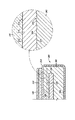
[0034]被膜210は、外側面212と内側面214とを含む。内側面214は、一般的に、本体202上に直接、配置される。一実施形態において、メッキ処理された被膜の厚さは、約0.3から約2.16ミルの間である。この範囲の外側に該当する厚さを持つメッキ処理された被膜は、失敗する可能性温度サイクル中に該当するか、或いは、PECVD堆積において形成されたSiN、αSi、n+α−Si製の大領域膜におけるスポッティングを十分に減少させない。
[0034] The
[0035]上記基板支持面204の上方に位置決めされた外側面212の一部218は、上部の基板140を支持するように構成された何学的形状を有する。外側面212の一部218は、所定の表面粗さの表面仕上げ処理部216を有し、これが、基板140上に堆積された膜の均一な厚さを促進する。表面処理仕上げ部216は、約80〜約200ミクロインチの粗さを有する。表面仕上げ処理部216は、有利なことに、改善膜の厚さ均一性が生じ、特に、基板支持体をコンディショニング(例えば、エージング)することなく、局所的厚さの不均一性(薄い堆積箇所)を実質的に除去することが分かってきた。基板支持体のコンディショニングの除去により、通常はプラズマエージング処理で消費される時間と材料の両方を節約でき、サイクル間の真空パージを除去し、この除去により、システムスループットが改善される。一実施形態において、表面仕上げ処理部216は、約130ミクロインチの粗さを有する。
[0035] A
[0036]メッキ処理された被膜の表面仕上げ処理部216は、基板140の下にある外側基板支持面204の少なくとも一部を処置することにより、更に/又は、(所定の表面仕上げ処理部208を得るために)基板140を支持するメッキ処理された被膜210を少なくとも処置することにより、達成可能である。基板支持面204の表面仕上げ処理部208は、数多くの方法で形成可能であり、例えば、ビードブラスト処理、研磨材ブラスト処理、研削、エンボス加工、サンディング、テクスチャリング、エッチング、所定の表面粗さを提供する他の方法がある。一実施形態において、本体202の支持面の表面仕上げ処理部208は、約88から約230ミクロインチである。他の実施形態において、表面仕上げ処理部208は、約145ミクロインチである。
[0036] The plated
[0037]オプションとして、基板140の下方から位置決めされる部分220を制限する基板支持面204のストリップ224は、製造コストを最小にするため、処置せずに残してもよい。これにより、未処置ストリップ224の上方に、メッキ処理された被膜210のストリップ222が生じるが、未処理ストリップ224は、仕上げ部216とは異なる仕上げ部を有し、ストリップ222は基板140を超え、ストリップ222の表面仕上げ処理部は、膜堆積の均一性に影響がない。一実施形態において、メッキ処理された被膜210のストリップ222は、それが制限する被膜210の一部218よりスムーズな表面仕上げ処理部を有する。
[0037] Optionally, the strip 224 of the
[0038]図3は、支持用アセンブリ138を製造するための方法300の一実施形態を示す。この方法は、本体202の支持面204を準備することにより、ステップ302から開始する。準備するステップ302は、一般的に、基板表面204を加工すること、或いは、他の方法で処置することを要するので、仕上げ処理部208は、約80から約200ミクロインチになっている。一実施形態において、準備するステップ302は、ビードブラスト処理、研磨材ブラスト処理、研削、エンボス加工、サンディング、テクスチャリング、エッチング、所定の表面粗さ(例えば、約130ミクロインチ)を与える他の方法を含んでもよい。
FIG. 3 illustrates one embodiment of a
[0039]一実施形態において、基板支持面204は、所定表面仕上げ状態までビードブラスト処理される。ビードブラスト処理は、本体202をセラミック又は酸化物ビードで衝突させることを含んでもよい。
[0039] In one embodiment, the
[0040]他の実施形態において、ビードは、平均径約125から375ミクロの酸化アルミニウムである。ビーズは、約88から約230ミクロインチの表面仕上げを提供するのに十分な出口速度を有するノズルを通して提供される。 [0040] In another embodiment, the bead is aluminum oxide having an average diameter of about 125 to 375 micro. The beads are provided through a nozzle having an exit velocity sufficient to provide a surface finish of about 88 to about 230 microinches.
[0041]準備するステップ302の後、本体はステップ304でメッキ処理される。メッキ処理するステップ304は、一般的に、約0.3から約2.16ミルの間の厚さを有するメッキ処理された層を適用するステップを含む。メッキ処理された被膜212の外側面212の、結果として生じる表面仕上げ処理部216は、約80から約200ミクロインチであり、一実施形態では、約130ミクロインチである。
[0041] After the preparing
[0042]図4は、支持用アセンブリ138を製造する方法400の他の実施形態である。この方法は、アルミニウム本体202をメッキ処理することによりステップ402で開始する。ステップ404では、メッキ処理された被膜210の外側面212の少なくとも一部218が処置され、粗くされた表面仕上げ処理部216を提供する。また、外側面212の他の部分は、処置されてもよい。
FIG. 4 is another embodiment of a
[0043]処理するステップ404は、ビードブラスト処理、研磨材ブラスト処理、研削、エンボス加工、サンディング、テクスチャリング、エッチング、所定の表面粗さを与える他の方法を含んでもよい。一実施形態において、処理するステップ404は、約80から約200ミクロインチ間の外側面の表面仕上げ処理部が生じる。
[0043] The
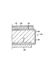
[0044]図5は、均一体積厚さを高めるように構成された支持用アセンブリ500の他の実施形態の一部断面図を示す。支持用アセンブリ500は、メッキ処理された被膜506により実質的に封入されたアルミニウム製支持用本体502を含む。加熱素子504は、支持用本体502に結合され、支持用アセンブリ500の上面に位置決めされた基板140の温度を制御する。加熱素子504は、抵抗加熱ヒータ、又は本体502に結合されるか本体502に配置される他の温度制御装置でもよい。代替え的に、加熱素子504と本体502との間に直接の接触を与えるために、本体502の下部512はメッキ処理が無くてもよい。オプションとして、熱伝導材の介在層(図示せず)が、加熱素子504と本体502の下部504の間に配置されてもよい。
[0044] FIG. 5 illustrates a partial cross-sectional view of another embodiment of a
[0045]基板140を支持する、メッキ処理された被膜506の上部508は、基板140上の均一な膜の堆積を高めるように構成された表面仕上げ処理部510を有する。一実施形態において、表面仕上げ処理部510は、約80から約200ミクロインチの間の粗さを有する。表面仕上げ処理部510は、前述した方法を含む数多くの方法を介して作り出せる。
[0045] The top 508 of the plated
[0046]図6は、加熱アセンブリ600の他の実施形態を示す。加熱アセンブリ600は、少なくとも部分的に上部に形成された、メッキ処理された被膜606を有するアルミニウム本体602を含む。加熱素子604,即ち、温度制御された流体が循環される導管は、本体602の底面に配置され、基板140の温度制御を容易にする。代替え的に、熱伝導板614は、加熱素子604と本体602との間に配置可能であり、加熱素子604と本体602間の温度均一性を高める。一実施形態において、介在層614は銅板である。
[0046] FIG. 6 shows another embodiment of a
[0047]クランプ板608は、複数のファスナ610(図6には一つが図示)であって、本体602に形成されたネジ付き孔612内に通されたものにより本体602に結合されている。クランプ板608は、加熱素子604を本体602を用いて挟み、熱伝達を高めている。
[0047] The
[0048]基板140を支持するメッキ処理された被膜606の一部620は、基板140の堆積膜の均一性を高めるように構成された表面仕上げ処理部622を有する。表面仕上げ処理部622は、前述したものと同様に作り出せる。
[0048] A
[0049]そのため、大領域基板上に配置された堆積膜の均一性を高める支持用アセンブリが提供される。基板を支持する支持用アセンブリのアルミニウム製本体を覆う、メッキ処理された被膜の少なくとも一部は、堆積均一性を高める所定の表面粗さまで織地状の表面にされ、それにより、実質的に時間消費する支持用アセンブリのエージングや付随するコストを除去する。 [0049] As such, a support assembly is provided that enhances the uniformity of the deposited film disposed on the large area substrate. At least a portion of the plated coating covering the aluminum body of the support assembly that supports the substrate is textured to a predetermined surface roughness that enhances deposition uniformity, thereby substantially time consuming. Eliminates aging and associated costs of supporting assemblies.
[0050]本発明の教示を組み込む幾つかの好適な実施形態を図示し詳細に説明してきたが、当業者は、容易に多くの他の変更実施形態であって、これらの教示を組み込むものを案出することができる。 [0050] While several preferred embodiments incorporating the teachings of the present invention have been shown and described in detail, those skilled in the art will readily recognize many other alternative embodiments that incorporate these teachings. Can be devised.
100…プラズマ増強型化学気相堆積システム、102…チャンバ、106…壁、108…底部、110…アセンブリ、112…処理ボリューム、114…ポンピングプレナム、116…第1補強部材、118…分配用プレート、120…内側、124…本体、126…下側、128…孔、130…電源、132…加熱素子、134…上側、138…基板支持用アセンブリ、140…大領域ガラス基板、142…ステム、144…ステムカバー、146…ベローズ、148…外接シャドウフレーム、150…リフトピン、154…リフトプレート、156…カラー、160…第1端部、164…第2端部、166…第2補強部材、168…上部、170…下部、180…被膜、190…熱電対、200…支持用アセンブリ、202…本体、204…支持面、206…装着面、208…表面仕上げ処理部、210…被膜、212…外側面、214…内側面、216…表面仕上げ処理部、218…部分、220…部分、224…ストリップ、500…支持用アセンブリ、502…アルミニウム製支持用本体、504…加熱素子、506…被膜、508…上部、510…表面仕上げ処理部、512…下部、600…ヒータアセンブリ、602…アルミニウム製本体、604…加熱素子、606…被膜、608…クランプ板、610…ファスナ、612…ネジ付き孔、614…介在層、620…部分、622…表面仕上げ処理部。
DESCRIPTION OF
Claims (25)
基板支持面を有する電気的導電性本体と;
前記本体に配置された電気絶縁性被膜と;
前記基板支持面の中央部を覆って配置された前記被膜の少なくとも一部は、約80〜約200ミクロインチ(25.4×10⁻⁶ミリ)の表面仕上げ処理部を有する、前記基板支持体。 In the substrate support:
An electrically conductive body having a substrate support surface;
An electrically insulating coating disposed on the body;
The substrate support, wherein at least a portion of the coating disposed over a central portion of the substrate support surface has a surface finishing treatment of about 80 to about 200 microinches (25.4 × 10 −6 mm). .
前記基板支持面上の中央に置かれた前記被膜の一部に外接し、約130ミクロインチ未満の表面仕上げを有するストリップを更に備える、請求項1記載の基板支持体。 The coating disposed on the substrate support surface is:
The substrate support of claim 1, further comprising a strip circumscribing a portion of the coating centered on the substrate support surface and having a surface finish of less than about 130 microinches.
約88から約230ミクロインチの間の表面仕上げ処理部を持つ中央領域と;
前記中央領域に外接させ、約130ミクロインチ未満の表面仕上げ処理部を有する周辺領域と;
を更に備える、請求項1記載の基板支持体。 The substrate support surface is:
A central region having a surface finish between about 88 and about 230 microinches;
A peripheral region circumscribing the central region and having a surface finish of less than about 130 microinches;
The substrate support according to claim 1, further comprising:
堆積後に約80〜200ミクロインチの表面仕上げに処置された前記基板支持面上に堆積された電気的に絶縁性の被膜と;
を備える、基板支持体。 An electrically conductive body having a substrate support surface;
An electrically insulating coating deposited on the substrate support surface treated to a surface finish of about 80-200 microinches after deposition;
A substrate support comprising:
前記処置された基板支持面上に堆積され、メッキ処理された被膜と;
を備える、基板支持体。 An aluminum body having a substrate support surface treated to a surface finish of about 88 to about 230 microinches;
A coating deposited on the treated substrate support surface and plated;
A substrate support comprising:
大領域の基板を支持するのに適した導電性本体を提供するステップと;
前記基板支持体の表面を被膜するステップであって、前記被膜が約80〜約200ミクロインチの表面粗さを有する、前記基板支持体。 A substrate support produced by the following method, said method:
Providing a conductive body suitable for supporting a large area substrate;
Coating the surface of the substrate support, wherein the coating has a surface roughness of about 80 to about 200 microinches.
アルミニウムから構成された本体をメッキ処理するステップを更に備える、請求項13記載の基板支持体。 The coating step includes:
The substrate support according to claim 13, further comprising a step of plating a main body made of aluminum.
表面粗さを約80〜約200ミクロインチにする為に前記被膜を処置するステップを更に備える、請求項13記載の基板支持体。 The steps of coating the surface of the substrate support include:
The substrate support of claim 13, further comprising treating the coating to achieve a surface roughness of about 80 to about 200 microinches.
前記メッキ処理された被膜を、ビードブラスト処理、研磨材ブラスト処理、研削、エンボス加工、サンディング、テクスチャリング、エッチングの少なくとも一つにより処置するステップを更に備える、請求項10記載の基板支持体。 The steps of treating the coating are:
The substrate support according to claim 10, further comprising a step of treating the plated film by at least one of bead blasting, abrasive blasting, grinding, embossing, sanding, texturing, and etching.
ビードブラスト処理、研磨材ブラスト処理、研削、エンボス加工、サンディング、テクスチャリング、エッチングの少なくとも一つを更に備える、請求項17記載の基板支持体。 The steps of treating the substrate support surface include:
The substrate support according to claim 17, further comprising at least one of bead blasting, abrasive blasting, grinding, embossing, sanding, texturing, and etching.
前記基板支持面をビードブラスト処理するステップを更に備える、請求項17記載の基板支持体。 The steps of treating the substrate support surface include:
The substrate support according to claim 17, further comprising a step of bead blasting the substrate support surface.
約125から約375ミクロンを平均径とするビーズで前記基板支持面に衝撃を与えるステップを更に備える、請求項19記載の基板支持体。 The steps of bead blasting the substrate support surface include:
20. The substrate support of claim 19, further comprising impacting the substrate support surface with beads having an average diameter of about 125 to about 375 microns.
約250ミクロンを平均径とするアルミニウム酸化物製ビーズで前記基板支持面に衝撃を与えるステップを更に備える、請求項19記載の基板支持体。 The steps of bead blasting the substrate support surface include:
The substrate support of claim 19, further comprising impacting the substrate support surface with aluminum oxide beads having an average diameter of about 250 microns.
約88〜約230ミクロインチの表面仕上げを得る為に、大領域基板を支持するように適合されたアルミニウム基板支持面を処置するステップと;
前記基板支持面を約0.3から約2.16ミルの厚さにメッキ処理するステップであって、前記基板支持面の中央部分を少なくとも覆って配置された前記メッキ被膜の表面仕上げは、約80〜約200ミクロインチの間の表面仕上げを有する、前記ステップと;
を備える、前記基板支持体。 A substrate support manufactured by the following method, said method:
Treating an aluminum substrate support surface adapted to support a large area substrate to obtain a surface finish of about 88 to about 230 microinches;
Plating the substrate support surface to a thickness of about 0.3 to about 2.16 mils, wherein the surface finish of the plated coating disposed over at least a central portion of the substrate support surface is about Said step having a surface finish of between 80 and about 200 microinches;
The substrate support comprising:
Applications Claiming Priority (1)
| Application Number | Priority Date | Filing Date | Title |
|---|---|---|---|
| US10/435,182 US20040221959A1 (en) | 2003-05-09 | 2003-05-09 | Anodized substrate support |
Related Child Applications (1)
| Application Number | Title | Priority Date | Filing Date |
|---|---|---|---|
| JP2009149983A Division JP2009239300A (en) | 2003-05-09 | 2009-06-24 | Anodized substrate support |
Publications (2)
| Publication Number | Publication Date |
|---|---|
| JP2005051200A true JP2005051200A (en) | 2005-02-24 |
| JP2005051200A5 JP2005051200A5 (en) | 2008-11-06 |
Family
ID=32990571
Family Applications (2)
| Application Number | Title | Priority Date | Filing Date |
|---|---|---|---|
| JP2004140365A Pending JP2005051200A (en) | 2003-05-09 | 2004-05-10 | Anodized substrate support |
| JP2009149983A Pending JP2009239300A (en) | 2003-05-09 | 2009-06-24 | Anodized substrate support |
Family Applications After (1)
| Application Number | Title | Priority Date | Filing Date |
|---|---|---|---|
| JP2009149983A Pending JP2009239300A (en) | 2003-05-09 | 2009-06-24 | Anodized substrate support |
Country Status (6)
| Country | Link |
|---|---|
| US (2) | US20040221959A1 (en) |
| EP (1) | EP1475460A1 (en) |
| JP (2) | JP2005051200A (en) |
| KR (2) | KR20040096785A (en) |
| CN (1) | CN100385640C (en) |
| TW (1) | TW200507157A (en) |
Cited By (3)
| Publication number | Priority date | Publication date | Assignee | Title |
|---|---|---|---|---|
| JP2007051367A (en) * | 2005-07-15 | 2007-03-01 | Applied Materials Inc | Reducing electrostatic charge by roughening susceptor |
| JP2008138283A (en) * | 2006-12-01 | 2008-06-19 | Applied Materials Inc | Plasma reactor substrate mounting surface texturing |
| US8372205B2 (en) | 2003-05-09 | 2013-02-12 | Applied Materials, Inc. | Reducing electrostatic charge by roughening the susceptor |
Families Citing this family (33)
| Publication number | Priority date | Publication date | Assignee | Title |
|---|---|---|---|---|
| US20040221959A1 (en) * | 2003-05-09 | 2004-11-11 | Applied Materials, Inc. | Anodized substrate support |
| JP2005064284A (en) * | 2003-08-14 | 2005-03-10 | Asm Japan Kk | Semiconductor substrate holding device |
| TWI287279B (en) * | 2004-09-20 | 2007-09-21 | Applied Materials Inc | Diffuser gravity support |
| US7732056B2 (en) * | 2005-01-18 | 2010-06-08 | Applied Materials, Inc. | Corrosion-resistant aluminum component having multi-layer coating |
| US8173228B2 (en) * | 2006-01-27 | 2012-05-08 | Applied Materials, Inc. | Particle reduction on surfaces of chemical vapor deposition processing apparatus |
| US20070202636A1 (en) * | 2006-02-22 | 2007-08-30 | Applied Materials, Inc. | Method of controlling the film thickness uniformity of PECVD-deposited silicon-comprising thin films |
| KR100812047B1 (en) * | 2006-08-14 | 2008-03-10 | 삼성에스디아이 주식회사 | Substrate driver and substrate moving method using the same |
| US7959735B2 (en) * | 2007-02-08 | 2011-06-14 | Applied Materials, Inc. | Susceptor with insulative inserts |
| US20080289686A1 (en) * | 2007-05-23 | 2008-11-27 | Tae Kyung Won | Method and apparatus for depositing a silicon layer on a transmitting conductive oxide layer suitable for use in solar cell applications |
| US7964430B2 (en) * | 2007-05-23 | 2011-06-21 | Applied Materials, Inc. | Silicon layer on a laser transparent conductive oxide layer suitable for use in solar cell applications |
| FR2922899B1 (en) * | 2007-10-26 | 2010-11-26 | Univ Toulouse | METHOD FOR MANUFACTURING POROUS STRUCTURE ORDERED FROM AN ALUMINUM SUBSTRATE |
| US9917001B2 (en) * | 2008-01-21 | 2018-03-13 | Applied Materials, Inc. | High temperature fine grain aluminum heater |
| KR101588566B1 (en) * | 2008-03-20 | 2016-01-26 | 어플라이드 머티어리얼스, 인코포레이티드 | Susceptor with roll-formed surface and method for making same |
| US20100000684A1 (en) * | 2008-07-03 | 2010-01-07 | Jong Yong Choi | Dry etching apparatus |
| US8597084B2 (en) * | 2008-10-16 | 2013-12-03 | Applied Materials, Inc. | Textured platen |
| US10392718B2 (en) | 2009-09-04 | 2019-08-27 | Apple Inc. | Anodization and polish surface treatment |
| KR101992702B1 (en) * | 2010-10-28 | 2019-06-25 | 어플라이드 머티어리얼스, 인코포레이티드 | High purity aluminum coating hard anodization |
| JP2012222287A (en) * | 2011-04-13 | 2012-11-12 | Shimadzu Corp | Plasma cvd deposition apparatus and substrate mounting device |
| KR102101192B1 (en) * | 2012-07-27 | 2020-04-21 | 어플라이드 머티어리얼스, 인코포레이티드 | Roughened substrate support |
| EP3944307A1 (en) * | 2012-10-01 | 2022-01-26 | Forced Physics Llc | Device for temperature control |
| US9850591B2 (en) | 2013-03-14 | 2017-12-26 | Applied Materials, Inc. | High purity aluminum top coat on substrate |
| US9624593B2 (en) | 2013-08-29 | 2017-04-18 | Applied Materials, Inc. | Anodization architecture for electro-plate adhesion |
| US9663870B2 (en) * | 2013-11-13 | 2017-05-30 | Applied Materials, Inc. | High purity metallic top coat for semiconductor manufacturing components |
| US9975320B2 (en) * | 2014-01-13 | 2018-05-22 | Applied Materials, Inc. | Diffusion bonded plasma resisted chemical vapor deposition (CVD) chamber heater |
| CN103956349B (en) * | 2014-05-20 | 2016-06-15 | 株洲南车时代电气股份有限公司 | The copper metalized structures of power semiconductor chip and making method thereof |
| JP6170029B2 (en) * | 2014-11-07 | 2017-07-26 | トヨタ自動車株式会社 | Method for forming a thermal barrier film |
| CN107201507B (en) * | 2016-03-17 | 2019-09-17 | Asm知识产权私人控股有限公司 | Substrate support plate and film deposition equipment comprising it |
| KR102632725B1 (en) | 2016-03-17 | 2024-02-05 | 에이에스엠 아이피 홀딩 비.브이. | Substrate support plate, thin film deposition apparatus including the same, and thin film deposition method |
| KR102652258B1 (en) * | 2016-07-12 | 2024-03-28 | 에이비엠 주식회사 | Metal component and manufacturing method thereof and process chamber having the metal component |
| US11330673B2 (en) | 2017-11-20 | 2022-05-10 | Applied Materials, Inc. | Heated substrate support |
| US10914114B2 (en) * | 2018-07-06 | 2021-02-09 | Guardian Glass, LLC | Electric potentially-driven shade including shutter supporting surface-modified conductive coating, and/or method of making the same |
| CN109881184B (en) * | 2019-03-29 | 2022-03-25 | 拓荆科技股份有限公司 | Substrate bearing device with electrostatic force suppression |
| US11521834B2 (en) * | 2020-08-26 | 2022-12-06 | Tokyo Electron Limited | Plasma processing systems and methods for chemical processing a substrate |
Family Cites Families (96)
| Publication number | Priority date | Publication date | Assignee | Title |
|---|---|---|---|---|
| US3019522A (en) * | 1958-06-23 | 1962-02-06 | John M Bluth | Reformation of metallic surfaces |
| US3616310A (en) * | 1969-03-10 | 1971-10-26 | Kaiser Aluminium Chem Corp | Aluminum-anodizing process |
| JPS59117675U (en) * | 1983-01-24 | 1984-08-08 | 旭可鍛鉄株式会社 | Structure of anodized film on aluminum or its alloy |
| US4801785A (en) * | 1986-01-14 | 1989-01-31 | Raychem Corporation | Electrical devices |
| US5200157A (en) * | 1986-02-17 | 1993-04-06 | Toshiba Ceramics Co., Ltd. | Susceptor for vapor-growth deposition |
| DE3714517A1 (en) * | 1987-04-30 | 1988-11-17 | Oberdorfer Fa F | THREAD SEPARATOR FOR SEAMING MACHINES, IN PARTICULAR FOR SEAMING DRAINAGE SCREENS, DRY SCREENS, FELTS AND THE LIKE |
| US4862799A (en) * | 1987-11-13 | 1989-09-05 | Rockwell International Corporation | Copper coated anodized aluminum ink metering roller |
| US5314601A (en) * | 1989-06-30 | 1994-05-24 | Eltech Systems Corporation | Electrodes of improved service life |
| JPH0686662B2 (en) | 1989-11-02 | 1994-11-02 | イビデン株式会社 | CVD susceptor |
| US4974369A (en) * | 1990-06-28 | 1990-12-04 | William Dixon | Two-dimensionally grooved sanding pad |
| US5104014A (en) * | 1990-06-28 | 1992-04-14 | John F. Flynn | Trapunto rod to stuff quilted items |
| US5395342A (en) * | 1990-07-26 | 1995-03-07 | Yoon; Inbae | Endoscopic portal |
| JP2748181B2 (en) * | 1990-07-26 | 1998-05-06 | キヤノン株式会社 | Wafer chuck |
| SU1797027A1 (en) | 1990-07-27 | 1993-02-23 | Ni Elektrotekh I | Semiconductor transducer of gas composition and its manufacturing technology |
| US5104514A (en) * | 1991-05-16 | 1992-04-14 | The United States Of America As Represented By The Secretary Of The Navy | Protective coating system for aluminum |
| JP3142619B2 (en) * | 1991-12-09 | 2001-03-07 | 株式会社設備デザイン建築設備士事務所 | Manufacturing method of exterior anodized building materials |
| US5290424A (en) * | 1992-01-31 | 1994-03-01 | Aluminum Company Of America | Method of making a shaped reflective aluminum strip, doubly-protected with oxide and fluoropolymer coatings |
| US5401319A (en) * | 1992-08-27 | 1995-03-28 | Applied Materials, Inc. | Lid and door for a vacuum chamber and pretreatment therefor |
| US5401573A (en) * | 1992-11-30 | 1995-03-28 | Mcdonnell Douglas Corporation | Protection of thermal control coatings from ultraviolet radiation |
| US5366585A (en) * | 1993-01-28 | 1994-11-22 | Applied Materials, Inc. | Method and apparatus for protection of conductive surfaces in a plasma processing reactor |
| US5384682A (en) * | 1993-03-22 | 1995-01-24 | Toto Ltd. | Electrostatic chuck |
| FR2714234B1 (en) * | 1993-12-16 | 1996-08-23 | Telemecanique | Power control system for an asynchronous motor. |
| US20020148941A1 (en) * | 1994-02-17 | 2002-10-17 | Boris Sorokov | Sputtering method and apparatus for depositing a coating onto substrate |
| US5581874A (en) * | 1994-03-28 | 1996-12-10 | Tokyo Electron Limited | Method of forming a bonding portion |
| JP3176219B2 (en) | 1994-05-31 | 2001-06-11 | 京セラ株式会社 | Electrostatic chuck |
| EP0693709A1 (en) * | 1994-07-18 | 1996-01-24 | Minnesota Mining And Manufacturing Company | Fluoropolymers and fluorochemical surface active agents for improving the antistatic behaviour of materials and light sensitive material having improved antistatic behaviour |
| US5548470A (en) * | 1994-07-19 | 1996-08-20 | International Business Machines Corporation | Characterization, modeling, and design of an electrostatic chuck with improved wafer temperature uniformity |
| US5756222A (en) * | 1994-08-15 | 1998-05-26 | Applied Materials, Inc. | Corrosion-resistant aluminum article for semiconductor processing equipment |
| US5677253A (en) * | 1995-03-30 | 1997-10-14 | Kyocera Corporation | Wafer holding member |
| US5804253A (en) * | 1995-07-17 | 1998-09-08 | Kanegafuchi Chemical Ind. Co., Ltd. | Method for adhering or sealing |
| US6355554B1 (en) * | 1995-07-20 | 2002-03-12 | Samsung Electronics Co., Ltd. | Methods of forming filled interconnections in microelectronic devices |
| US6077781A (en) * | 1995-11-21 | 2000-06-20 | Applied Materials, Inc. | Single step process for blanket-selective CVD aluminum deposition |
| JPH09168171A (en) * | 1995-12-14 | 1997-06-24 | Semiconductor Energy Lab Co Ltd | Display device and its display system |
| US5844205A (en) * | 1996-04-19 | 1998-12-01 | Applied Komatsu Technology, Inc. | Heated substrate support structure |
| EP0803900A3 (en) * | 1996-04-26 | 1999-12-29 | Applied Materials, Inc. | Surface preparation to enhance the adhesion of a dielectric layer |
| JPH09323234A (en) | 1996-06-05 | 1997-12-16 | Nippon Cement Co Ltd | Electrostatic chuck and manufacture thereof |
| US5856236A (en) * | 1996-06-14 | 1999-01-05 | Micron Technology, Inc. | Method of depositing a smooth conformal aluminum film on a refractory metal nitride layer |
| US5916454A (en) * | 1996-08-30 | 1999-06-29 | Lam Research Corporation | Methods and apparatus for reducing byproduct particle generation in a plasma processing chamber |
| US6007673A (en) * | 1996-10-02 | 1999-12-28 | Matsushita Electronics Corporation | Apparatus and method of producing an electronic device |
| US6537905B1 (en) * | 1996-12-30 | 2003-03-25 | Applied Materials, Inc. | Fully planarized dual damascene metallization using copper line interconnect and selective CVD aluminum plug |
| US6055927A (en) * | 1997-01-14 | 2000-05-02 | Applied Komatsu Technology, Inc. | Apparatus and method for white powder reduction in silicon nitride deposition using remote plasma source cleaning technology |
| US5858464A (en) * | 1997-02-13 | 1999-01-12 | Applied Materials, Inc. | Methods and apparatus for minimizing excess aluminum accumulation in CVD chambers |
| JP3160229B2 (en) * | 1997-06-06 | 2001-04-25 | 日本エー・エス・エム株式会社 | Susceptor for plasma CVD apparatus and method for manufacturing the same |
| FR2764310B1 (en) * | 1997-06-10 | 1999-07-09 | Commissariat Energie Atomique | MULTI-LAYERED MATERIAL WITH ANTI-EROSION, ANTI-ABRASION, AND ANTI-WEAR COATING ON AN ALUMINUM, MAGNESIUM OR ALLOY SUBSTRATE |
| US6024044A (en) * | 1997-10-09 | 2000-02-15 | Applied Komatsu Technology, Inc. | Dual frequency excitation of plasma for film deposition |
| JP3283459B2 (en) * | 1997-12-17 | 2002-05-20 | 日本エー・エス・エム株式会社 | Substrate holding device for semiconductor processing |
| US6064031A (en) * | 1998-03-20 | 2000-05-16 | Mcdonnell Douglas Corporation | Selective metal matrix composite reinforcement by laser deposition |
| US6184489B1 (en) * | 1998-04-13 | 2001-02-06 | Nec Corporation | Particle-removing apparatus for a semiconductor device manufacturing apparatus and method of removing particles |
| JP3588253B2 (en) * | 1998-06-04 | 2004-11-10 | 京セラ株式会社 | Electrostatic chuck |
| US6117772A (en) * | 1998-07-10 | 2000-09-12 | Ball Semiconductor, Inc. | Method and apparatus for blanket aluminum CVD on spherical integrated circuits |
| DE19839997C1 (en) * | 1998-09-02 | 2000-06-21 | Siemens Ag | Electronic circuitry |
| FR2783970B1 (en) * | 1998-09-25 | 2000-11-03 | Commissariat Energie Atomique | DEVICE AUTHORIZING THE PROCESSING OF A SUBSTRATE IN A MACHINE PROVIDED FOR PROCESSING LARGER SUBSTRATES AND SYSTEM FOR MOUNTING A SUBSTRATE IN THIS DEVICE |
| US6081874A (en) * | 1998-09-29 | 2000-06-27 | International Business Machines Corporation | Non-uniform memory access (NUMA) data processing system that speculatively issues requests on a node interconnect |
| US6726304B2 (en) * | 1998-10-09 | 2004-04-27 | Eastman Kodak Company | Cleaning and repairing fluid for printhead cleaning |
| JP3438625B2 (en) * | 1998-12-10 | 2003-08-18 | マックス株式会社 | Prevention of looseness of reel wound wire for reinforcing bar binding |
| JP2001209981A (en) * | 1999-02-09 | 2001-08-03 | Ricoh Co Ltd | Device and method for forming optical disk substrate film, manufacturing method for substrate holder, substrate holder, optical disk and phase change recording optical disk |
| KR100476845B1 (en) | 1999-04-06 | 2005-03-17 | 동경 엘렉트론 주식회사 | Electrode, wafer stage, plasma device, method of manufacturing electrode and wafer stage |
| TW465017B (en) * | 1999-04-13 | 2001-11-21 | Applied Materials Inc | A corrosion-resistant protective coating for an apparatus and method for processing a substrate |
| JP3911902B2 (en) * | 1999-04-16 | 2007-05-09 | 東京エレクトロン株式会社 | Processing apparatus and surface treatment method for metal parts |
| US6322712B1 (en) * | 1999-09-01 | 2001-11-27 | Micron Technology, Inc. | Buffer layer in flat panel display |
| US6423175B1 (en) * | 1999-10-06 | 2002-07-23 | Taiwan Semiconductor Manufacturing Co., Ltd | Apparatus and method for reducing particle contamination in an etcher |
| US6649031B1 (en) * | 1999-10-08 | 2003-11-18 | Hybrid Power Generation Systems, Llc | Corrosion resistant coated fuel cell bipolar plate with filled-in fine scale porosities and method of making the same |
| US6196001B1 (en) * | 1999-10-12 | 2001-03-06 | Alliedsignal Inc. | Environment controlled WIP cart |
| JP2001117079A (en) | 1999-10-18 | 2001-04-27 | Ibiden Co Ltd | Heating device of substrate for liquid crystal display plate |
| US6207558B1 (en) * | 1999-10-21 | 2001-03-27 | Applied Materials, Inc. | Barrier applications for aluminum planarization |
| US6775873B2 (en) * | 2000-02-09 | 2004-08-17 | Eugene H. Luoma | Apparatus for removing hair from a drain |
| WO2001071784A1 (en) | 2000-03-17 | 2001-09-27 | Hitachi, Ltd. | Method of manufacturing semiconductor and manufacturing apparatus |
| JP2001298013A (en) | 2000-04-13 | 2001-10-26 | Sharp Corp | Substrate processing device |
| JP2001355072A (en) * | 2000-06-13 | 2001-12-25 | Anelva Corp | Substrate treatment apparatus |
| SG106588A1 (en) * | 2000-10-10 | 2004-10-29 | Inst Data Storage | Method for producing thin film magnetic devices having increased orientation ratio |
| US6470508B2 (en) * | 2000-11-08 | 2002-10-29 | Watkins Manufacturing Corporation | Air check valve system for a spa |
| US6554907B2 (en) * | 2001-01-02 | 2003-04-29 | Applied Materials, Inc. | Susceptor with internal support |
| TWI272689B (en) | 2001-02-16 | 2007-02-01 | Tokyo Electron Ltd | Method and apparatus for transferring heat from a substrate to a chuck |
| JP3758979B2 (en) * | 2001-02-27 | 2006-03-22 | 京セラ株式会社 | Electrostatic chuck and processing apparatus |
| JP4359001B2 (en) * | 2001-03-02 | 2009-11-04 | 本田技研工業株式会社 | Anodized film modification method, anodized film structure, and aluminum alloy outboard motor |
| US6458683B1 (en) * | 2001-03-30 | 2002-10-01 | Taiwan Semiconductor Manufacturing Co., Ltd | Method for forming aluminum bumps by CVD and wet etch |
| JP2002313781A (en) | 2001-04-11 | 2002-10-25 | Sumitomo Electric Ind Ltd | Substrate treating equipment |
| KR100422446B1 (en) * | 2001-07-12 | 2004-03-12 | 삼성전자주식회사 | Exhaust ring of dry etch device |
| US20030047464A1 (en) * | 2001-07-27 | 2003-03-13 | Applied Materials, Inc. | Electrochemically roughened aluminum semiconductor processing apparatus surfaces |
| KR100789453B1 (en) | 2001-07-30 | 2008-01-02 | 엘지.필립스 엘시디 주식회사 | Plasma cvd process chamber |
| US6510888B1 (en) * | 2001-08-01 | 2003-01-28 | Applied Materials, Inc. | Substrate support and method of fabricating the same |
| TW589401B (en) * | 2001-10-24 | 2004-06-01 | Hon Hai Prec Ind Co Ltd | The surface treatment of aluminum article |
| JP3635463B2 (en) | 2001-11-27 | 2005-04-06 | 東京エレクトロン株式会社 | Self-bias measurement method and apparatus, and electrostatic chuck |
| US7048814B2 (en) * | 2002-02-08 | 2006-05-23 | Applied Materials, Inc. | Halogen-resistant, anodized aluminum for use in semiconductor processing apparatus |
| US7033447B2 (en) * | 2002-02-08 | 2006-04-25 | Applied Materials, Inc. | Halogen-resistant, anodized aluminum for use in semiconductor processing apparatus |
| US6776873B1 (en) * | 2002-02-14 | 2004-08-17 | Jennifer Y Sun | Yttrium oxide based surface coating for semiconductor IC processing vacuum chambers |
| US8067067B2 (en) * | 2002-02-14 | 2011-11-29 | Applied Materials, Inc. | Clean, dense yttrium oxide coating protecting semiconductor processing apparatus |
| US6659331B2 (en) * | 2002-02-26 | 2003-12-09 | Applied Materials, Inc | Plasma-resistant, welded aluminum structures for use in semiconductor apparatus |
| US6565984B1 (en) * | 2002-05-28 | 2003-05-20 | Applied Materials Inc. | Clean aluminum alloy for semiconductor processing equipment |
| KR100557882B1 (en) | 2002-10-10 | 2006-03-10 | 김종균 | Sliding door opening/closing apparatus |
| US6884336B2 (en) * | 2003-01-06 | 2005-04-26 | General Motors Corporation | Color finishing method |
| KR200312050Y1 (en) | 2003-01-29 | 2003-05-01 | 이기봉 | Laser detector using cigarette jack of automobile |
| US8372205B2 (en) * | 2003-05-09 | 2013-02-12 | Applied Materials, Inc. | Reducing electrostatic charge by roughening the susceptor |
| US20040221959A1 (en) * | 2003-05-09 | 2004-11-11 | Applied Materials, Inc. | Anodized substrate support |
| US7732056B2 (en) * | 2005-01-18 | 2010-06-08 | Applied Materials, Inc. | Corrosion-resistant aluminum component having multi-layer coating |
| KR200432489Y1 (en) | 2006-09-22 | 2006-12-04 | 김원석 | Apparatus for controlling water level of rice field |
-
2003
- 2003-05-09 US US10/435,182 patent/US20040221959A1/en not_active Abandoned
-
2004
- 2004-05-06 TW TW093112801A patent/TW200507157A/en unknown
- 2004-05-08 KR KR1020040032489A patent/KR20040096785A/en not_active Application Discontinuation
- 2004-05-09 CN CNB2004100347390A patent/CN100385640C/en active Active
- 2004-05-10 EP EP04011066A patent/EP1475460A1/en not_active Withdrawn
- 2004-05-10 JP JP2004140365A patent/JP2005051200A/en active Pending
-
2006
- 2006-04-18 US US11/406,136 patent/US7732010B2/en active Active
- 2006-07-27 KR KR1020060070677A patent/KR20060100302A/en not_active Application Discontinuation
-
2009
- 2009-06-24 JP JP2009149983A patent/JP2009239300A/en active Pending
Cited By (3)
| Publication number | Priority date | Publication date | Assignee | Title |
|---|---|---|---|---|
| US8372205B2 (en) | 2003-05-09 | 2013-02-12 | Applied Materials, Inc. | Reducing electrostatic charge by roughening the susceptor |
| JP2007051367A (en) * | 2005-07-15 | 2007-03-01 | Applied Materials Inc | Reducing electrostatic charge by roughening susceptor |
| JP2008138283A (en) * | 2006-12-01 | 2008-06-19 | Applied Materials Inc | Plasma reactor substrate mounting surface texturing |
Also Published As
| Publication number | Publication date |
|---|---|
| US20040221959A1 (en) | 2004-11-11 |
| JP2009239300A (en) | 2009-10-15 |
| CN1551326A (en) | 2004-12-01 |
| CN100385640C (en) | 2008-04-30 |
| TW200507157A (en) | 2005-02-16 |
| EP1475460A1 (en) | 2004-11-10 |
| US7732010B2 (en) | 2010-06-08 |
| KR20040096785A (en) | 2004-11-17 |
| KR20060100302A (en) | 2006-09-20 |
| US20060185795A1 (en) | 2006-08-24 |
Similar Documents
| Publication | Publication Date | Title |
|---|---|---|
| US7732010B2 (en) | Method for supporting a glass substrate to improve uniform deposition thickness | |
| JP2005051200A5 (en) | ||
| US8372205B2 (en) | Reducing electrostatic charge by roughening the susceptor | |
| KR101441858B1 (en) | Reducing electrostatic charge by roughening the susceptor | |
| KR100431658B1 (en) | Apparatus for heating a substrate and apparatus having the same | |
| US20020134511A1 (en) | Substrate supporting table,method for producing same, and processing system | |
| US20060005771A1 (en) | Apparatus and method of shaping profiles of large-area PECVD electrodes | |
| US5626678A (en) | Non-conductive alignment member for uniform plasma processing of substrates | |
| EP1928017B1 (en) | Plasma reactor substrate mounting surface texturing | |
| US7815492B2 (en) | Surface treatment method | |
| KR101139165B1 (en) | Ti FILM FORMING METHOD AND STORAGE MEDIUM | |
| JP5745394B2 (en) | Substrate support, plasma reactor, and method of forming a susceptor | |
| JPH09199488A (en) | Processing device | |
| TW200834688A (en) | Prevention of film deposition on PECVD process chamber wall | |
| JP2523070B2 (en) | Plasma processing device | |
| CN111139458A (en) | Deposition device | |
| JP2002093790A (en) | Method and device for manufacturing semiconductor device | |
| US20230386883A1 (en) | Methods and apparatus for minimizing substrate backside damage | |
| JP2005330518A (en) | Plasma treatment device | |
| JPS60102742A (en) | Controller for substrate temperature | |
| JP2003297912A (en) | Substrate treatment device | |
| JP2002110571A (en) | Film forming apparatus and film forming method | |
| KR20070080766A (en) | Apparatus and method for treating a substrate | |
| WO2007023535A1 (en) | Method of film formation, mask for film formation and film formation apparatus |
Legal Events
| Date | Code | Title | Description |
|---|---|---|---|
| A521 | Request for written amendment filed |
Free format text: JAPANESE INTERMEDIATE CODE: A523 Effective date: 20050913 |
|
| A621 | Written request for application examination |
Free format text: JAPANESE INTERMEDIATE CODE: A621 Effective date: 20050913 |
|
| A131 | Notification of reasons for refusal |
Free format text: JAPANESE INTERMEDIATE CODE: A131 Effective date: 20080617 |
|
| A524 | Written submission of copy of amendment under article 19 pct |
Free format text: JAPANESE INTERMEDIATE CODE: A524 Effective date: 20080917 |
|
| A02 | Decision of refusal |
Free format text: JAPANESE INTERMEDIATE CODE: A02 Effective date: 20090224 |