EP4299507A2 - Dichtung für mikroelektronische anordnung - Google Patents
Dichtung für mikroelektronische anordnung Download PDFInfo
- Publication number
- EP4299507A2 EP4299507A2 EP23191206.4A EP23191206A EP4299507A2 EP 4299507 A2 EP4299507 A2 EP 4299507A2 EP 23191206 A EP23191206 A EP 23191206A EP 4299507 A2 EP4299507 A2 EP 4299507A2
- Authority
- EP
- European Patent Office
- Prior art keywords
- seal
- microelectronic
- wafer
- cavity
- microelectronic component
- Prior art date
- Legal status (The legal status is an assumption and is not a legal conclusion. Google has not performed a legal analysis and makes no representation as to the accuracy of the status listed.)
- Granted
Links
Images


Classifications
-
- H—ELECTRICITY
- H01—ELECTRIC ELEMENTS
- H01L—SEMICONDUCTOR DEVICES NOT COVERED BY CLASS H10
- H01L23/00—Details of semiconductor or other solid state devices
- H01L23/02—Containers; Seals
- H01L23/10—Containers; Seals characterised by the material or arrangement of seals between parts, e.g. between cap and base of the container or between leads and walls of the container
-
- B—PERFORMING OPERATIONS; TRANSPORTING
- B81—MICROSTRUCTURAL TECHNOLOGY
- B81C—PROCESSES OR APPARATUS SPECIALLY ADAPTED FOR THE MANUFACTURE OR TREATMENT OF MICROSTRUCTURAL DEVICES OR SYSTEMS
- B81C1/00—Manufacture or treatment of devices or systems in or on a substrate
- B81C1/00015—Manufacture or treatment of devices or systems in or on a substrate for manufacturing microsystems
- B81C1/00261—Processes for packaging MEMS devices
- B81C1/00277—Processes for packaging MEMS devices for maintaining a controlled atmosphere inside of the cavity containing the MEMS
- B81C1/00293—Processes for packaging MEMS devices for maintaining a controlled atmosphere inside of the cavity containing the MEMS maintaining a controlled atmosphere with processes not provided for in B81C1/00285
-
- B—PERFORMING OPERATIONS; TRANSPORTING
- B81—MICROSTRUCTURAL TECHNOLOGY
- B81B—MICROSTRUCTURAL DEVICES OR SYSTEMS, e.g. MICROMECHANICAL DEVICES
- B81B7/00—Microstructural systems; Auxiliary parts of microstructural devices or systems
- B81B7/0032—Packages or encapsulation
-
- B—PERFORMING OPERATIONS; TRANSPORTING
- B81—MICROSTRUCTURAL TECHNOLOGY
- B81B—MICROSTRUCTURAL DEVICES OR SYSTEMS, e.g. MICROMECHANICAL DEVICES
- B81B7/00—Microstructural systems; Auxiliary parts of microstructural devices or systems
- B81B7/0032—Packages or encapsulation
- B81B7/0074—3D packaging, i.e. encapsulation containing one or several MEMS devices arranged in planes non-parallel to the mounting board
-
- B—PERFORMING OPERATIONS; TRANSPORTING
- B81—MICROSTRUCTURAL TECHNOLOGY
- B81C—PROCESSES OR APPARATUS SPECIALLY ADAPTED FOR THE MANUFACTURE OR TREATMENT OF MICROSTRUCTURAL DEVICES OR SYSTEMS
- B81C1/00—Manufacture or treatment of devices or systems in or on a substrate
- B81C1/00015—Manufacture or treatment of devices or systems in or on a substrate for manufacturing microsystems
- B81C1/00261—Processes for packaging MEMS devices
- B81C1/00269—Bonding of solid lids or wafers to the substrate
-
- B—PERFORMING OPERATIONS; TRANSPORTING
- B81—MICROSTRUCTURAL TECHNOLOGY
- B81C—PROCESSES OR APPARATUS SPECIALLY ADAPTED FOR THE MANUFACTURE OR TREATMENT OF MICROSTRUCTURAL DEVICES OR SYSTEMS
- B81C1/00—Manufacture or treatment of devices or systems in or on a substrate
- B81C1/00015—Manufacture or treatment of devices or systems in or on a substrate for manufacturing microsystems
- B81C1/00261—Processes for packaging MEMS devices
- B81C1/00333—Aspects relating to packaging of MEMS devices, not covered by groups B81C1/00269 - B81C1/00325
-
- H—ELECTRICITY
- H01—ELECTRIC ELEMENTS
- H01L—SEMICONDUCTOR DEVICES NOT COVERED BY CLASS H10
- H01L23/00—Details of semiconductor or other solid state devices
- H01L23/02—Containers; Seals
-
- H—ELECTRICITY
- H01—ELECTRIC ELEMENTS
- H01L—SEMICONDUCTOR DEVICES NOT COVERED BY CLASS H10
- H01L23/00—Details of semiconductor or other solid state devices
- H01L23/02—Containers; Seals
- H01L23/04—Containers; Seals characterised by the shape of the container or parts, e.g. caps, walls
-
- H—ELECTRICITY
- H01—ELECTRIC ELEMENTS
- H01L—SEMICONDUCTOR DEVICES NOT COVERED BY CLASS H10
- H01L23/00—Details of semiconductor or other solid state devices
- H01L23/02—Containers; Seals
- H01L23/04—Containers; Seals characterised by the shape of the container or parts, e.g. caps, walls
- H01L23/053—Containers; Seals characterised by the shape of the container or parts, e.g. caps, walls the container being a hollow construction and having an insulating or insulated base as a mounting for the semiconductor body
-
- B—PERFORMING OPERATIONS; TRANSPORTING
- B81—MICROSTRUCTURAL TECHNOLOGY
- B81C—PROCESSES OR APPARATUS SPECIALLY ADAPTED FOR THE MANUFACTURE OR TREATMENT OF MICROSTRUCTURAL DEVICES OR SYSTEMS
- B81C2203/00—Forming microstructural systems
- B81C2203/01—Packaging MEMS
- B81C2203/0109—Bonding an individual cap on the substrate
-
- B—PERFORMING OPERATIONS; TRANSPORTING
- B81—MICROSTRUCTURAL TECHNOLOGY
- B81C—PROCESSES OR APPARATUS SPECIALLY ADAPTED FOR THE MANUFACTURE OR TREATMENT OF MICROSTRUCTURAL DEVICES OR SYSTEMS
- B81C2203/00—Forming microstructural systems
- B81C2203/01—Packaging MEMS
- B81C2203/0118—Bonding a wafer on the substrate, i.e. where the cap consists of another wafer
-
- B—PERFORMING OPERATIONS; TRANSPORTING
- B81—MICROSTRUCTURAL TECHNOLOGY
- B81C—PROCESSES OR APPARATUS SPECIALLY ADAPTED FOR THE MANUFACTURE OR TREATMENT OF MICROSTRUCTURAL DEVICES OR SYSTEMS
- B81C2203/00—Forming microstructural systems
- B81C2203/01—Packaging MEMS
- B81C2203/0172—Seals
- B81C2203/019—Seals characterised by the material or arrangement of seals between parts
-
- B—PERFORMING OPERATIONS; TRANSPORTING
- B81—MICROSTRUCTURAL TECHNOLOGY
- B81C—PROCESSES OR APPARATUS SPECIALLY ADAPTED FOR THE MANUFACTURE OR TREATMENT OF MICROSTRUCTURAL DEVICES OR SYSTEMS
- B81C2203/00—Forming microstructural systems
- B81C2203/03—Bonding two components
- B81C2203/033—Thermal bonding
- B81C2203/035—Soldering
-
- B—PERFORMING OPERATIONS; TRANSPORTING
- B81—MICROSTRUCTURAL TECHNOLOGY
- B81C—PROCESSES OR APPARATUS SPECIALLY ADAPTED FOR THE MANUFACTURE OR TREATMENT OF MICROSTRUCTURAL DEVICES OR SYSTEMS
- B81C2203/00—Forming microstructural systems
- B81C2203/03—Bonding two components
- B81C2203/033—Thermal bonding
- B81C2203/036—Fusion bonding
-
- B—PERFORMING OPERATIONS; TRANSPORTING
- B81—MICROSTRUCTURAL TECHNOLOGY
- B81C—PROCESSES OR APPARATUS SPECIALLY ADAPTED FOR THE MANUFACTURE OR TREATMENT OF MICROSTRUCTURAL DEVICES OR SYSTEMS
- B81C2203/00—Forming microstructural systems
- B81C2203/03—Bonding two components
- B81C2203/038—Bonding techniques not provided for in B81C2203/031 - B81C2203/037
Definitions
- the following description relates to processing of integrated circuits ("ICs"). More particularly, the following description relates to devices and techniques for processing IC dies and assemblies.
- devices commonly referred to as "smart phones” integrate the functions of a cellular telephone with powerful data processors, memory and ancillary devices such as global positioning system receivers, electronic cameras, a variety of sensors, and local area network connections along with high-resolution displays and associated image processing chips.
- Such devices can provide capabilities such as full internet connectivity, entertainment including full-resolution video, navigation, electronic banking and more, all in a pocket-size device.
- Complex portable devices require packing numerous chips and dies into a small space.
- Microelectronic elements often comprise a thin slab of a semiconductor material, such as silicon or gallium arsenide. Chips and dies are commonly provided as individual, prepackaged units. In some unit designs, the die is mounted to a substrate or a chip carrier, which is in turn mounted on a circuit panel, such as a printed circuit board (PCB). Dies can be provided in packages that facilitate handling of the die during manufacture and during mounting of the die on the external substrate. For example, many dies are provided in packages suitable for surface mounting.
- solder packages of this general type have been proposed for various applications.
- a dielectric element commonly referred to as a "chip carrier” with terminals formed as plated or etched metallic structures on the dielectric.
- the terminals typically are connected to the contacts (e.g., bond pads) of the die by conductive features such as thin traces extending along the die carrier and by fine leads or wires extending between the contacts of the die and the terminals or traces.
- the package may be placed onto a circuit board so that each terminal on the package is aligned with a corresponding contact pad on the circuit board. Solder or other bonding material is generally provided between the terminals and the contact pads.
- the package can be permanently bonded in place by heating the assembly so as to melt or "reflow" the solder or otherwise activate the bonding material.
- solder masses in the form of solder balls that are typically between about 0.02 mm and about 0.8 mm (5 and 30 mils) in diameter, and are attached to the terminals of the package.
- a package having an array of solder balls projecting from its bottom surface (e.g., surface opposite the front face of the die) is commonly referred to as a ball grid array or "BGA” package.
- BGA ball grid array
- LGA land grid array
- packages are secured to the substrate by thin layers or lands formed from solder.
- Packages of this type can be quite compact.
- Certain packages, commonly referred to as "chip scale packages” occupy an area of the circuit board equal to, or only slightly larger than, the area of the device incorporated in the package. This scale is advantageous in that it reduces the overall size of the assembly and permits the use of short interconnections between various devices on the substrate, which in turn limits signal propagation time between devices and thus facilitates operation of the assembly at high speeds.
- Semiconductor dies can also be provided in "stacked" arrangements, wherein one die is provided on a carrier, for example, and another die is mounted on top of the first die. These arrangements can allow a number of different dies to be mounted within a single footprint on a circuit board and can further facilitate high-speed operation by providing a short interconnection between the dies. Often, this interconnect distance can be only slightly longer than the thickness of the die itself.
- interconnection structures for mechanical and electrical connection may be provided on both sides (e.g., surfaces) of each die package (except, perhaps, for the topmost package).
- TSVs Through Silicon Vias
- dies or wafers may be bonded in a stacked arrangement using various bonding techniques, including direct dielectric bonding, non-adhesive techniques, such as ZiBond ® or a hybrid bonding technique, such as DBI ® , both available from Invensas Bonding Technologies, Inc. (formerly Ziptronix, Inc.), an Xperi company (see for example, U.S. Patent No. 6,864,585 and 7,485,968 , which are incorporated herein in their entirety).
- various bonding techniques including direct dielectric bonding, non-adhesive techniques, such as ZiBond ® or a hybrid bonding technique, such as DBI ® , both available from Invensas Bonding Technologies, Inc. (formerly Ziptronix, Inc.), an Xperi company (see for example, U.S. Patent No. 6,864,585 and 7,485,968 , which are incorporated herein in their entirety).
- Stacked die and wafer arrangements may also be used to form assembled components such as microelectromechanical systems (MEMS), sensors, and the like. See, for example, U.S. Patent No. 7109092 , which is incorporated herein in its entirety.
- MEMS microelectromechanical systems
- devices and systems illustrated in the figures are shown as having a multiplicity of components.
- Various implementations of devices and/or systems, as described herein, may include fewer components and remain within the scope of the disclosure.
- other implementations of devices and/or systems may include additional components, or various combinations of the described components, and remain within the scope of the disclosure.
- Seals are disposed at joined (e.g., bonded, coupled, etc.) surfaces of stacked dies and wafers to seal (e.g., hermetically seal) the joined surfaces.
- the joined surfaces may be sealed to form sensor cavities, or the like, as part of the microelectronic devices. For instance, when a die with a recessed surface is bonded to another die with a flat surface or a recessed surface, a cavity can be formed between the two dies. In some applications, it may be desirable for this cavity to be hermetically sealed, to maintain a specific vacuum level inside the cavity and for predetermined leak rates to be maintained.
- the leak rate of a sealed cavity can be looked at as a function of the cavity's volume. For example, if the volume of a cavity is less than or equal to 0.01 cc, generally, the leak rate is to be below 5E-8 atm-cc/s of air to consider the cavity hermetically sealed. If the volume of the cavity ranges between 0.01 and 0.4 cc, the leak rate is to be below 1E-7, and if the volume is greater than 0.4 cc, then the leak rate is to be below 1E-6 for a hermetically sealed cavity (per MIL-STD-883 Method 1014, MIL-STD-750 Method 1071).
- the integrity of a seal at the periphery of a stack of dies can be critical to maintain the application specific hermeticity and low leak rates of the package.
- Metals, ceramics, and glasses are the typical materials used to form the seal and to prevent water vapor or other gases (e.g. oxygen, etc.) from accessing components inside the package.
- a properly made hermetic seal with a sufficiently low leak rate can keep the interior of a package dry and moisture free for many years.
- the techniques disclosed herein include forming seals of one or more metallic materials (for example) at a joint (e.g., a bond line, a seam, etc.) of at least two surfaces, which seals the joined surfaces at the joint.
- metallic materials may be deposited using electroless plating, or the like.
- metallic materials may be deposited directly onto the joined surfaces at or around the joint.
- one or more non-metallic materials may be deposited onto the joined surfaces, and metallic material can be deposited over the non-metallic material(s), sealing the j oint.
- the seal may include a continuous sealing ring formed completely around joined dies or wafers (e.g., a periphery of the devices) or one or more partial seals, as desired.
- the techniques disclosed can seal dies and wafers that are stacked and bonded using "ZIBOND ® " techniques, which can benefit from the added seal.
- a cavity wafer 102 is bonded to a microelectromechanical system (MEMS) wafer 104 (or any other wafer) using a ZIBOND ® technique, for example, to form a microelectronic device 100 such as a MEMS sensor device.
- MEMS microelectromechanical system
- a cavity wafer 102 (or a die) may have 1 or more cavities or recesses of the same or varying size.
- Especially-flat surfaces of the two wafers (102 and 104) are bonded together using a low temperature covalent bond between the two corresponding semiconductor and/or insulator layers.
- the bond may be good, the seal may not be adequate as a hermetic seal, and the leak rates may not be as low as desired for the application. Further, the bond line width (P1) may not be optimal, since a relatively long bond line can unnecessarily increase the die size and can reduce the number of dies fabricated per wafer.
- the seal may be improved by forming one or more metal-to-metal interconnections along the bonding seam using a Direct Bond Interconnect (DBI ® ) technique.
- Metallic lines 106 are deposited along each of the surfaces to be joined, so as to be aligned to each other, and form metal-to-metal bonds when set together using temperature and/or pressure.
- the DBI lines 106 can help to reduce the bond line width (P2) while improving the hermeticity of the joint.
- the bond line width (P1) needed for utilizing a ZiBond method may not be adequate for the application (e.g., a 100 micron bond line width using Zibond may be reduced to tens of microns or less than 10 microns, using DBI for example). Further, such DBI bonds are not easy to achieve, potentially adding to the complexity and cost of the assembly.
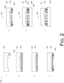
- FIG. 2 is a graphical flow diagram illustrating an example processing sequence 200 to form a stacked microelectronic device 100.
- the process 200 and the stacked microelectronic device 100 form a background for discussing various sealing techniques and devices.
- the process 200 described with reference to FIG. 2 may be modified to include the techniques and devices for hermetically sealing bonded components at the bond joints.
- FIG. 2 describes the process for a 3 die stack creating a hermetically sealed cavity 202 between top (and middle) and (middle and) bottom die. But a stack could also include only 2 dies with a cavity 202 between them, as depicted in FIG. 1 .
- a recessed cavity wafer 102 is formed. Although one cavity 202 is shown in the illustration at block 1, one or more cavities 202 of similar or different dimensions may be formed per die location, effectively forming several such recessed cavities 202 on a wafer (or die) 102.
- the cavity wafer 102 is bonded to a MEMS wafer 104 (or any other wafer or die) closing the cavity 202 within.
- the cavity wafer 102 can be bonded to the MEMS wafer 104 using an intimate surface bonding technique, for example, a ZIBOND ® technique, wherein insulating surfaces (e.g., SiOx - SiOx, etc.) are bonded.
- the MEMS wafer 104 may be thinned and patterned to form stand-offs.
- metallization 204 can be added to the patterned surface of the MEMS wafer 104, including pads, contacts, traces, and so forth. In an alternate example, no metallization 204 is added to the surface of the MEMS wafer 104.
- the microelectronic device 100 can be attached to another device, such as a logic device wafer, for example, using a Zibond technique (e.g., SiOx - SiOx bond) or the like at the bonded surfaces, or using other bonding techniques for dielectrics (such as a polymeric material, e.g. die attached film or paste) on one or both bonded surfaces.
- a Zibond technique e.g., SiOx - SiOx bond
- dielectrics such as a polymeric material, e.g. die attached film or paste
- openings are formed in the MEMS wafer 104, accessing the cavity 202, to define the characteristics of the microelectronic device 100, based on the application.
- the microelectronic device 100 can be attached to a logic device wafer (or die) 206, to provide logic/control (for example) for the microelectronic device 100.
- Metallization layer 204 contact pads of the microelectronic device 100 are coupled to contacts 208 on the surface of the logic device 206.
- portions of the microelectronic device 100 (such as portions of the cavity wafer 102) are removed (e.g., etched, etc.) to provide access to other contact pads of the logic device wafer 206, and so forth.
- the Zibond or DBI interface between the cavity wafer 102 and the MEMS wafer 104 may provide an adequate resistance to the flow of fluids, such as gases and/or liquids.
- one or more of the bond lines or coupling joints of the microelectronic device 100 can be sealed for hermeticity (e.g., a predetermined resistance to the flow of fluids, such as gases and/or liquids, and sufficiently low moisture vapor transmission rate, oxygen transmission rate, etc.), as discussed below.
- the techniques disclosed herein include bonding insulator surfaces of the wafers (e.g., 102 and 104), then adding a metallic seal at the bond line to improve the hermeticity, as discussed further below.
- FIG. 3 shows example embodiments of sealing a microelectronic device 100, such as the microelectronic device 100 formed with reference to FIG. 2 .
- a metallic seal ring 302 can be formed surrounding the bonded joint of the cavity wafer 102 and the MEMS wafer 104, and can also be extended to seal the logic device 206 to the MEMS wafer 104.
- the seal ring 302 creates a hermetic seal around a periphery of the microelectronic components (e.g., 102, 104, and 206), fully sealing the joints between the components.
- the seal ring 302 can be located to seal any or all of the joints between the microelectronic components (e.g., 102, 104, and 206), as desired.
- the seal ring 302 is comprised of a metallic material (i.e., a metal such as copper, for example, an alloy, or a metallic composition). In some embodiments, two or more metallic materials may be used in layers (or other combinations) to form the seal ring 302. In the various embodiments, the seal ring 302 is deposited using electroless plating, electrodeposition, mechanical printing, or various combinations thereof, or the like.
- a metallic material i.e., a metal such as copper, for example, an alloy, or a metallic composition.
- two or more metallic materials may be used in layers (or other combinations) to form the seal ring 302.
- the seal ring 302 is deposited using electroless plating, electrodeposition, mechanical printing, or various combinations thereof, or the like.
- multiple seal rings 302 may be used to seal between multiple components (e.g., 102, 104, 206, and 304) at different stacking levels in a stacked microelectronic arrangement 300. Seal rings 302 may be used at any or all of the levels of the stacked arrangement 300, as desired. While complete seal rings 302 are discussed and illustrated, partial seal rings 302 may also be used where desired to form seals at bond joints or between components (e.g., 102, 104, 206, and 304) of a microelectronic device (e.g., 100, 300) or assembly.
- a microelectronic device e.g., 100, 300
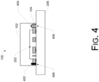
- FIG. 4 shows an example sealed microelectronic device 100, according to another embodiment, using interior seals (e.g., 402 and 404).
- interior seals e.g., 402 and 404
- interior seals are formed after drilling, etching, or otherwise forming a channel 406 (fully or partially) around an inside perimeter of the bonded components (e.g., 102, 104, and 206).
- Two separate configurations of example seals are illustrated in FIG. 4 , a filled seal 402 and a conformal seal 404. Both configurations are formed in channels 406, drilled portions, or the like, as discussed further below.
- the filled seal ring 402 mostly or fully fills the channel 406 or drilled cavity with one or more metallic materials to form the hermetic seal at the bond joint.
- the conformal seal ring 404 plates the walls of the channel 406 or cavity with the one or more metallic materials to form the hermetic seal.
- either the filled seal 404 or the conformal seal 406 may be used to hermetically seal two or more components (e.g., 102, 104, and 206), as desired.
- multiple concentric seal rings e.g., 302, 402, and 404 may be used to seal two (or more) components (e.g., 102, 104, and 206).
- the channel(s) 406 may extend through component 104 and to the interface with component 102 or, shown, into component 102.
- FIG. 5 is a graphical flow diagram illustrating an example processing sequence 500 to form a sealed microelectronic device 100, according to an embodiment using interior seals (e.g., 402 and 404).
- the process 500 described with reference to FIG. 5 may be used to modify other assembly processes (e.g., the process 200 referred to at FIG. 2 , for example) that include bonding microelectronic components (e.g., 102, 104, 206, etc.), to include techniques and devices for hermetically sealing the bonded microelectronic components (e.g., 102, 104, 206, etc.) at the bond joints, as desired.
- bonding microelectronic components e.g., 102, 104, 206, etc.
- a recessed cavity wafer 102 is formed.
- a channel 406 (or "cavity ring,” partly or fully surrounding the cavity 202) is formed on the cavity-side surface of the wafer 102.
- the channel 406 may be formed by etching, drilling, or otherwise removing material from the surface of the wafer 102.
- the cavity wafer 102 is bonded to a MEMS wafer 104 closing the cavity 202 within.
- the cavity wafer 102 can be bonded to the MEMS wafer 104 using an intimate surface bonding technique, for example, such as a ZIBOND ® technique, wherein insulating surfaces (e.g., SiOx - SiOx, etc.) are bonded.
- the cavity wafer 102 can be bonded to the MEMS wafer 104 using another dielectric bonding technique (e.g. die attach film or paste, a polymeric material such as a silicone or epoxy, or the like, which may not provide a hermetic seal and may not improve or fix a hermetic seal).
- the MEMS wafer 104 may be thinned and patterned to form stand-offs.
- the stand-offs are optional and may not be formed on the MEMS wafer 104.
- the standoffs can be formed on the logic wafer 206 or can be created by any other material (e.g. die attach film or paste, etc.).
- openings are formed in the MEMS wafer 104, accessing the cavity 202, to define the characteristics of the microelectronic device 100, based on the application.
- channels 406 are formed in the MEMS wafer 104 (and in the cavity wafer 102, in some examples) for forming interior seals (e.g., 402 and 404) to seal the bonding joint between the cavity wafer 102 and the MEMS wafer 104.
- the MEMS wafer 104 can be drilled to open an area in the MEMS wafer 104 that is aligned with the cavity ring channel 406 previously formed in the cavity wafer 102.
- the MEMS wafer 104 and the cavity wafer 102 can be drilled together to form the cavity ring channel 406 (e.g., the channel 406 in the cavity wafer 102 is formed at this step, while drilling the MEMS wafer 104, rather than being pre-formed prior to bonding the cavity wafer 102 to the MEMS wafer 104).
- metallization 204 is added to the patterned surface of the MEMS wafer 104, including pads, contacts, traces, and so forth.
- the cavity ring channel 406 can also be metallized at this time.
- the channel 406 can be partially or fully filled/plated to form a filled seal ring 402, or the walls of the channel 406 can be metallized/plated to form a conformal seal ring 404. Either the filled seal ring 402 or the conformal seal ring 404 (whichever is used) hermetically seal the bond joint between the cavity wafer 102 and the MEMS wafer 104.
- the MEMS wafer 104 and the cavity wafer 102 can be drilled together to form the cavity ring channel 406, which can be metallized and then the openings to the cavity 202 are formed in the MEMS wafer 104.
- the microelectronic device 100 may be attached to a logic device 206, to provide logic/control (for example) for the microelectronic device 100.
- Contact pads of the metallized layer 204 of the microelectronic device 100 can be coupled to contacts 208 on the surface of the logic device 206.
- portions of the microelectronic device 100 may be removed (e.g., etched, etc.) to provide access to other contact pads of the logic device 206, and so forth.
- FIGS. 6A - 6E illustrate example embodiments of seals 302, 402, and 404 and sealed microelectronic devices 100, according to various embodiments.
- a first embodiment, illustrated at FIG. 6A shows exterior seals 302 implemented as discussed above with reference to FIGS. 3 and 4 .
- Each seal 302 forms a bead that covers one or more bonding or coupling joints between the microelectronic components 102, 104, and 206, to hermetically seal the joints.
- the seals 302 can be comprised of a metallic material such as a metal, an alloy, or a metal composite, for example a combination of two or more metals, a metal-glass composite material, a metal-ceramic composite, or the like.
- a second embodiment, illustrated at FIG. 6B shows seals having a layered approach, where a polymer seal 602 is applied to the exterior of the joint first and a metallic material seal 604 is deposited over the polymer seal 602, forming a hermetic seal.
- a polymer seal 602 is applied to the exterior of the joint first and a metallic material seal 604 is deposited over the polymer seal 602, forming a hermetic seal.
- multiple polymer materials forming one or more polymer seals 602 and/or multiple metallic layers forming one or more metallic seals 604 may also be used to form a seal ring.
- a third embodiment, illustrated at FIG. 6C shows another exterior seal ring 606, comprised of a sinterable conductive paste, a fritted glass composite, or the like.
- the metallic or glass components in the deposited seal 606 material provide the hermetic seal desired.
- a fourth embodiment, illustrated at FIG. 6D shows interior seals 402 and 404 as discussed above with reference to FIGS. 5 and 6 .
- a channel 406 is formed through the MEMS wafer 104 and into the cavity wafer 102, and the channel 406 is plated from the MEMS wafer 104 side with metallic material, either fully (e.g., 402), partially (not shown) or conformal (e.g., 404) to the channel 406 walls.
- a fifth embodiment, illustrated at FIG. 6E shows an example of forming a seal ring (e.g., 404) through multiple components (e.g., 102, 104, and 206).
- the logic wafer 206 (or the like) can be thinned and drilled through, similar to the MEMS wafer 104.
- the logic wafer 206, MEMS wafer 104, and cavity wafer 102 may be bonded in a process and then drilled together, or in separate steps to be aligned.
- Plating or filling the drilled channel 406 from the logic wafer 206 side forms a seal ring (e.g., 404) that extends from the logic wafer 206, through the MEMS wafer 104, and into the cavity wafer 102, hermetically sealing each of the bonding joints and the spaces between the components (e.g., 102, 104, and 206).
- the seal e.g., 404 may extend through only some of the layers/components as desired.
- the metallization of the seals may be electrically continuous with or coupled to one or more device pads, for grounding, or the like (which may also be electrically continuous with a ball terminal 608 (for example) on the package. While multiple types of metallization (conformal, nonconformal) are shown in FIGS. 6D, 6E and elsewhere in this disclosure, only a single type of metallization may be used at a time to form a continuous or discontinuous shape for inhibiting fluid flow and, thus, improving hermeticity.
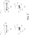
- FIGS. 7A - 7D illustrate example embodiments of seals 402 and 404 and sealed microelectronic devices 100, according to further embodiments.
- an embedded metallic ring 702 is partially or fully embedded within the cavity wafer 102 (and/or the MEMS wafer 104) and partially or fully surrounds the cavity 202.
- the embedded metallic ring 702, which may be disposed at or near the bond line, can aid in sealing the bond joint between the cavity wafer 102 and the MEMS wafer 104.
- a via (not shown for the sake of simplicity) may extend through cavity wafer 102 and contact the metallic ring 702.
- FIG. 7A illustrate example embodiments of seals 402 and 404 and sealed microelectronic devices 100, according to further embodiments.
- an embedded metallic ring 702 is partially or fully embedded within the cavity wafer 102 (and/or the MEMS wafer 104) and partially or fully surrounds the cavity 202.
- the embedded metallic ring 702 which may be disposed at or near the bond line, can aid in
- the microelectronic device 100 includes an embedded metallic ring 702 partially or fully surrounding the cavity 202, as well as one or more interior seals 402 and/or 404, as discussed above with reference to FIGS. 5 and 6 .
- a channel 406 is formed through the MEMS wafer 104 and into the cavity wafer 102, to the embedded metallic ring 702, and the channel 406 is plated from the MEMS wafer 104 side with metallic material, either fully (e.g., 402), partially (not shown) or conformal (e.g., 404) to the channel 406 walls.
- FIGS. 7C and 7D show close detail views of two possible embodiments (of many) for this arrangement.
- the channel 406 has a relatively rectangular cross-section
- the channel has a polygonal, or otherwise shaped cross-section (e.g., partially or fully elliptical, irregular, etc.).
- the width of the cross-section of the channel 406 and the seal (402 and/or 404), where the seal (402 and/or 404) makes contact with the embedded metallic ring 702, is less (e.g., 60% or less) than the width of the cross-section of the embedded metallic ring 702.
- the metallic fill for the seals 404 may be fully (as seen in FIG. 7C ) or partially (as seen in FIG. 7D ) lining the interior walls of the channel 406, while making contact with (landed on) the embedded metallic ring 702.
- the shape of the channel 406 may be predetermined, or may be a product of the drilling techniques employed to form the channel 406.
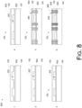
- FIG. 8 is a graphical flow diagram illustrating an example processing sequence 800 to form a sealed microelectronic device 100, according to another embodiment using interior seals (e.g., 806).
- the process 800 described with reference to FIG. 8 may be used to modify other assembly processes (e.g., the process 200 referred to at FIG. 2 , for example) that include bonding microelectronic components (e.g., 102, 104, 206, etc.), to include techniques and devices for hermetically sealing the bonded microelectronic components (e.g., 102, 104, 206, etc.) at the bond joints, as desired.
- bonding microelectronic components e.g., 102, 104, 206, etc.
- a recessed cavity wafer 102 is formed and prepared for bonding to a second wafer 104.
- the bonding surface of the second wafer 104 may include an added layer 802, such as an insulating layer, a dielectric layer, a semiconductor layer, a metallic layer, and so forth.
- the cavity wafer 102 is bonded to the second wafer 104, closing the cavity 202 within.
- the cavity wafer 102 can be bonded to the second wafer 104 (and the layer 802) using an intimate surface bonding technique, for example, such as a ZIBOND ® technique, wherein insulating surfaces (e.g., SiOx - SiOx, etc.) are bonded.
- the cavity wafer 102 can be bonded to the second wafer 104 using another dielectric bonding technique (e.g. die attach film or paste, a polymeric material such as a silicone or epoxy, or the like, which may not provide a hermetic seal and may not improve or fix a hermetic seal).
- the cavity wafer 102 and/or the second wafer 104 may be thinned based on the intended application.
- a coating or layer 804 such as a dielectric layer or the like, may be applied to the exposed surface of the cavity wafer 102.
- one or more channels 406 (or "cavity rings," partly or fully surrounding the cavities 202) can be formed through portions of the cavity wafer 102, portions of the second wafer 104, and through one or both of the layers 802 and 804.
- the channels 406 may be formed by etching, drilling, or otherwise removing material from the wafers 102 and 104, and may be open to an outside surface of the cavity wafer 102 or the second wafer 104.
- the cavity ring channels 406 can be partially or fully filled/plated with a metallic material (e.g., copper) to form filled seal rings 806.
- the filled seal rings 806 hermetically seal the bond joints between the cavity wafer 102 and the second wafer 104, sealing the cavities 202.
- the top exposed portion of the metallic seal rings 806 comprise a redistribution layer (RDL).
- FIG. 9A shows a sealed microelectronic device 100 wherein the bottom portion of the one or more filled seal rings 806 is disposed within the layer 802 (which may be a dielectric layer, for example), and may or may not penetrate the second wafer 104.
- An opposite end of the filled seal rings 806 e.g., at the top of the cavity wafer 102 may be exposed and contact a metal layer for electrical (and/or heat dissipation) function of the microelectronic device 100, for example.
- FIG. 9B shows another sealed microelectronic device 100 wherein the bottom portion of the filled seal rings 806 is disposed within the layer 802 (which may be a dielectric layer, for example), and may or may not penetrate the second wafer 104.
- the top portion of the filled seal rings 806 forms a redistribution layer (RDL) over a portion of the exposed surface of the cavity wafer 102.
- the dielectric layer 804 is patterned so that the dielectric layer 804 is not covering over the one or more cavities 202.
- FIG. 9C shows a further sealed microelectronic device 100 wherein the bottom portion of the filled seal rings 806 is disposed within the layer 802 (which may be a dielectric layer, for example), and may or may not penetrate the second wafer 104.
- the top portion of the filled seal rings 806 forms a redistribution layer (RDL) over one or more portions of the exposed surface of the cavity wafer 102.
- the dielectric layer 804 is patterned so that the dielectric layer 804 is not covering over the one or more cavities 202, however, a different layer 902 is arranged to cover over the cavities 202.
- the different layer 902 may comprise a substrate, a glass panel, a metallic layer, or the like.
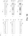
- FIG. 10 is a graphical flow diagram illustrating an example processing sequence 1000 to form a sealed microelectronic device 100, according to another embodiment using interior seals (e.g., 806).
- the process 1000 described with reference to FIG. 10 may be used to modify other assembly processes (e.g., the process 200 referred to at FIG. 2 , for example) that include bonding microelectronic components (e.g., 102, 104, 206, etc.), to include techniques and devices for hermetically sealing the bonded microelectronic components (e.g., 102, 104, 206, etc.) at the bond joints, as desired.
- bonding microelectronic components e.g., 102, 104, 206, etc.
- a recessed cavity wafer 102 is formed and prepared for bonding to a second wafer 104.
- the bonding surface of the second wafer 104 may include an added layer 802, such as an insulating layer, a dielectric layer, a semiconductor layer, a metallic layer, and so forth.
- the cavity wafer 102 is bonded to the second wafer 104, closing the cavity 202 within.
- the cavity wafer 102 can be bonded to the second wafer 104 (and the layer 802) using an intimate surface bonding technique, for example, such as a ZIBOND ® technique, wherein insulating surfaces (e.g., SiOx - SiOx, etc.) are bonded.
- the cavity wafer 102 can be bonded to the second wafer 104 using another dielectric bonding technique (e.g. die attach film or paste, a polymeric material such as a silicone or epoxy, or the like, which may not provide a hermetic seal and may not improve or fix a hermetic seal).
- the cavity wafer 102 and/or the second wafer 104 may be thinned based on the intended application. Further, the assembly featuring the cavity wafer 102 and the second wafer 104 may be flipped for processing from the second wafer 104 side.
- a coating or layer 804 such as a dielectric layer or the like, may be applied to the exposed surface of the second wafer 104.
- one or more channels 406 (or "cavity rings,” partly or fully surrounding the cavities 202) can be formed through portions of the second wafer 104, portions of the cavity wafer 102, and through one or both of the layers 802 and 804.
- the channels 406 may be formed by etching, drilling, or otherwise removing material from the wafers 102 and 104, and may be open to an outside surface of the second wafer 104 or the cavity wafer 102. As discussed above, the channels may extend only the interface between wafers (or dies) 102 and 104 and may extend to one or more metallic features such as a pad or via on or within wafer 104.
- the cavity ring channels 406 can be partially or fully filled/plated with a metallic material (e.g., copper) to form filled seal rings 806.
- the filled seal rings 806 hermetically seal the bond joints between the second wafer 104 and the cavity wafer 102, sealing the cavities 202.
- the top exposed portion of the metallic seal rings 806 may comprise a redistribution layer (RDL).
- FIGS. 11A - 11B embodiments of the sealed microelectronic device 100 are illustrated as examples.
- FIGS. 11A and 11B show sealed microelectronic devices 100 wherein the bottom portion of the filled seal rings 806 is disposed within the layer 802 (which may be a dielectric layer, for example), and may or may not penetrate the cavity wafer 102.
- An opposite end of the filled seal rings 806 e.g., at the top of the second wafer 104 may be exposed and contact a metal layer for electrical function of the microelectronic device 100, for example.
- the dielectric layer 804 is patterned so that the dielectric layer 804 is not covering over the one or more cavities 202, however, a different layer 902 is arranged to cover over the cavities 202.
- the different layer 902 may comprise a substrate, a glass panel, a metallic layer, or the like.
- the one or more cavities 202 extend into the second wafer 104 as well as the cavity wafer 102.
- the filled seal rings 806 hermetically seal the bond joints between the second wafer 104 and the cavity wafer 102, sealing the cavities 202.
- a metallic barrier layer 1102 may be applied within one or more of the cavities 202 to further seal the one or more cavities 202.
- the metallic barrier 1102 can be disposed on the side walls, or on the side, top, and bottom walls, partially or fully covering the inside surfaces of the cavities 202, as shown in FIG. 11B .
- the metallic barrier 1102 may be applied to the inside surfaces of the cavities 202 prior to bonding the cavity wafer 102 to the second wafer 104.
- the bonding process may include a metal-to-metal bonding (such as DBI, for instance), with or without a heated annealing, to bond the metallic barrier 1102 disposed on the inside surfaces of the cavity wafer 102 to the metallic barrier 1102 disposed on the inside surfaces of the second wafer 104, forming a continuous metallic sealing barrier 1102.
- FIG. 12 is a graphical flow diagram illustrating an example processing sequence 1200 to form a sealed microelectronic device 100, according to another embodiment using interior seals (e.g., 1202).
- the process 1200 described with reference to FIG. 12 may be used to modify other assembly processes (e.g., the process 200 referred to at FIG. 2 , for example) that include bonding microelectronic components (e.g., 102, 104, 206, etc.), to include techniques and devices for hermetically sealing the bonded microelectronic components (e.g., 102, 104, 206, etc.) at the bond joints, as desired.
- bonding microelectronic components e.g., 102, 104, 206, etc.
- a recessed cavity wafer 102 is formed and prepared for bonding to a second wafer 104 (which may or may not be a MEMS wafer, for example).
- the bonding surface of the second wafer 104 may include an added layer 802, such as an insulating layer, a dielectric layer, a semiconductor layer, a metallic layer, and so forth.
- the cavity wafer 102 is bonded to the second wafer 104, closing the cavity 202 within.
- the cavity wafer 102 can be bonded to the second wafer 104 (and the layer 802) using an intimate surface bonding technique, for example, such as a ZIBOND ® technique, wherein insulating surfaces (e.g., SiOx - SiOx, etc.) are bonded.
- the cavity wafer 102 can be bonded to the second wafer 104 using another dielectric bonding technique (e.g. die attach film or paste, a polymeric material such as a silicone or epoxy, or the like, which may not provide a hermetic seal and may not improve or fix a hermetic seal).
- the cavity wafer 102 and/or the second wafer 104 may be thinned based on the intended application.
- a coating or layer 804 such as a dielectric layer or the like, may be applied to the exposed surface of the cavity wafer 102.
- one or more channels 406 (or "cavity rings," partly or fully surrounding the cavities 202) can be formed through portions of the cavity wafer 102, portions of the second wafer 104, and through one or both of the layers 802 and 804.
- the channels 406 may be formed by etching, drilling, or otherwise removing material from the wafers 102 and 104, and may be open to an outside surface of the cavity wafer 102 or the second wafer 104.
- the cavity ring channels 406 can be partially filled/plated with a metallic material (e.g., copper) to form conformal seal rings 1202.
- the seal rings 1202 hermetically seal the bond joints between the cavity wafer 102 and the second wafer 104, sealing the cavities 202.
- the channels 406 can be filled/plated to form the conformal seal rings 1202 while a metallic layer 1204 is deposited onto at least a portion of the exposed surface of the cavity wafer 102. Accordingly, in various embodiments, the channels 406 are filled in the same or in separate processes as the deposition of the metallic layer 1204.
- FIGS. 13A - 13C show sealed microelectronic devices 100 wherein the seal rings 1202 are formed through the cavity layer 102, and the bottom portion of the seal rings 1202 is disposed through the layer 802 (which may be a dielectric layer, for example) and also penetrate the second wafer 104.
- FIGS. 13A and 13B show partially filled seal rings 1202 (e.g., plated in a vacuum, for example), with the embodiment shown at FIG. 13B having a greater quantity of metal within the partially filled seal rings 1202 than the embodiment shown at FIG. 13A .
- Annealing the substrates (bonded wafers 102 and 104) in the partially filled condition at temperatures between 80 and 250C can enlarge the grain size of the plated metal (e.g., 1202 and/or 1204).
- the process of producing the enlarged grain sizes can reduce impurities within the metal layer of the seal rings 1202 and/or the metallic layer 1204.
- the grains have a general (e.g., average) diameter that is greater than 10 percent of the width dimension of the channel 406.
- FIG. 13C shows fully filled seal rings 1202 within the channels 406.
- the annealed metal of the partially filled seal rings 1202, as shown in FIGS. 13A and 13B can be added to or coated with an additional metal layer to form the fully filled seal rings 1202.
- the sealed microelectronic device 100 may be annealed again after deposition of the additional metal layer.
- CMP may be used prior to the final annealing or afterwards, to form a desired surface for the filled seal rings 1202.
- One or more additional materials may be provided in the unfilled portion of the seal ring 1202, as needed, for reliability, robustness, performance, etc.
- the top (e.g., exposed) end of the filled seal rings 1202 may be exposed and contact a metal layer for electrical function of the microelectronic device 100, for example, when bonded to another device.
- seal rings 302, 402, 404, 806, and 1202 shown in the illustrations of FIGS. 1-13 are for example and discussion.
- a sealed microelectronic device 100 or like assembly may include fewer, or a greater quantity of seal rings 302, 402, 404, 806, and 1202, and remain within the scope of the disclosure.
- various implementations described herein may be combined to further enhance the improvement over conventional techniques of fabricating a MEMS device. For example, while seal rings are shown to extend into one surface from one side of the component, seal rings may be formed from both sides and may contact each other to form a metallic structure fully extending through the sealed microelectronic device 100.
Landscapes
- Engineering & Computer Science (AREA)
- Microelectronics & Electronic Packaging (AREA)
- Manufacturing & Machinery (AREA)
- Computer Hardware Design (AREA)
- Physics & Mathematics (AREA)
- General Physics & Mathematics (AREA)
- Condensed Matter Physics & Semiconductors (AREA)
- Power Engineering (AREA)
- Micromachines (AREA)
- Internal Circuitry In Semiconductor Integrated Circuit Devices (AREA)
- Combinations Of Printed Boards (AREA)
- Encapsulation Of And Coatings For Semiconductor Or Solid State Devices (AREA)
- Pressure Welding/Diffusion-Bonding (AREA)
Priority Applications (1)
| Application Number | Priority Date | Filing Date | Title |
|---|---|---|---|
| EP25196539.8A EP4628445A3 (de) | 2017-03-21 | 2018-03-15 | Dichtung für mikroelektronische anordnung |
Applications Claiming Priority (4)
| Application Number | Priority Date | Filing Date | Title |
|---|---|---|---|
| US201762474478P | 2017-03-21 | 2017-03-21 | |
| US15/920,759 US10508030B2 (en) | 2017-03-21 | 2018-03-14 | Seal for microelectronic assembly |
| PCT/US2018/022688 WO2018175208A1 (en) | 2017-03-21 | 2018-03-15 | Seal for microelectronic assembly |
| EP18772378.8A EP3607579B1 (de) | 2017-03-21 | 2018-03-15 | Dichtung für mikroelektronische anordnung |
Related Parent Applications (2)
| Application Number | Title | Priority Date | Filing Date |
|---|---|---|---|
| EP18772378.8A Division EP3607579B1 (de) | 2017-03-21 | 2018-03-15 | Dichtung für mikroelektronische anordnung |
| EP18772378.8A Division-Into EP3607579B1 (de) | 2017-03-21 | 2018-03-15 | Dichtung für mikroelektronische anordnung |
Related Child Applications (1)
| Application Number | Title | Priority Date | Filing Date |
|---|---|---|---|
| EP25196539.8A Division EP4628445A3 (de) | 2017-03-21 | 2018-03-15 | Dichtung für mikroelektronische anordnung |
Publications (3)
| Publication Number | Publication Date |
|---|---|
| EP4299507A2 true EP4299507A2 (de) | 2024-01-03 |
| EP4299507A3 EP4299507A3 (de) | 2024-04-10 |
| EP4299507B1 EP4299507B1 (de) | 2025-08-27 |
Family
ID=63582081
Family Applications (3)
| Application Number | Title | Priority Date | Filing Date |
|---|---|---|---|
| EP25196539.8A Pending EP4628445A3 (de) | 2017-03-21 | 2018-03-15 | Dichtung für mikroelektronische anordnung |
| EP18772378.8A Active EP3607579B1 (de) | 2017-03-21 | 2018-03-15 | Dichtung für mikroelektronische anordnung |
| EP23191206.4A Active EP4299507B1 (de) | 2017-03-21 | 2018-03-15 | Dichtung für mikroelektronische anordnung |
Family Applications Before (2)
| Application Number | Title | Priority Date | Filing Date |
|---|---|---|---|
| EP25196539.8A Pending EP4628445A3 (de) | 2017-03-21 | 2018-03-15 | Dichtung für mikroelektronische anordnung |
| EP18772378.8A Active EP3607579B1 (de) | 2017-03-21 | 2018-03-15 | Dichtung für mikroelektronische anordnung |
Country Status (5)
| Country | Link |
|---|---|
| US (6) | US10508030B2 (de) |
| EP (3) | EP4628445A3 (de) |
| JP (3) | JP7369037B2 (de) |
| TW (3) | TWI781061B (de) |
| WO (1) | WO2018175208A1 (de) |
Families Citing this family (92)
| Publication number | Priority date | Publication date | Assignee | Title |
|---|---|---|---|---|
| US7109092B2 (en) | 2003-05-19 | 2006-09-19 | Ziptronix, Inc. | Method of room temperature covalent bonding |
| US7485968B2 (en) | 2005-08-11 | 2009-02-03 | Ziptronix, Inc. | 3D IC method and device |
| US8735219B2 (en) | 2012-08-30 | 2014-05-27 | Ziptronix, Inc. | Heterogeneous annealing method and device |
| US20150262902A1 (en) | 2014-03-12 | 2015-09-17 | Invensas Corporation | Integrated circuits protected by substrates with cavities, and methods of manufacture |
| US11069734B2 (en) | 2014-12-11 | 2021-07-20 | Invensas Corporation | Image sensor device |
| US9741620B2 (en) | 2015-06-24 | 2017-08-22 | Invensas Corporation | Structures and methods for reliable packages |
| US10886250B2 (en) | 2015-07-10 | 2021-01-05 | Invensas Corporation | Structures and methods for low temperature bonding using nanoparticles |
| US9953941B2 (en) | 2015-08-25 | 2018-04-24 | Invensas Bonding Technologies, Inc. | Conductive barrier direct hybrid bonding |
| US10446532B2 (en) | 2016-01-13 | 2019-10-15 | Invensas Bonding Technologies, Inc. | Systems and methods for efficient transfer of semiconductor elements |
| US10204893B2 (en) | 2016-05-19 | 2019-02-12 | Invensas Bonding Technologies, Inc. | Stacked dies and methods for forming bonded structures |
| US10446487B2 (en) | 2016-09-30 | 2019-10-15 | Invensas Bonding Technologies, Inc. | Interface structures and methods for forming same |
| US10607136B2 (en) | 2017-08-03 | 2020-03-31 | Xcelsis Corporation | Time borrowing between layers of a three dimensional chip stack |
| US10580735B2 (en) | 2016-10-07 | 2020-03-03 | Xcelsis Corporation | Stacked IC structure with system level wiring on multiple sides of the IC die |
| US10672663B2 (en) | 2016-10-07 | 2020-06-02 | Xcelsis Corporation | 3D chip sharing power circuit |
| TWI892323B (zh) | 2016-10-27 | 2025-08-01 | 美商艾德亞半導體科技有限責任公司 | 用於低溫接合的結構和方法 |
| US10002844B1 (en) | 2016-12-21 | 2018-06-19 | Invensas Bonding Technologies, Inc. | Bonded structures |
| US20180182665A1 (en) | 2016-12-28 | 2018-06-28 | Invensas Bonding Technologies, Inc. | Processed Substrate |
| WO2018125673A2 (en) | 2016-12-28 | 2018-07-05 | Invensas Bonding Technologies, Inc | Processing stacked substrates |
| TW202431592A (zh) | 2016-12-29 | 2024-08-01 | 美商艾德亞半導體接合科技有限公司 | 具有整合式被動構件的接合結構 |
| WO2018147940A1 (en) | 2017-02-09 | 2018-08-16 | Invensas Bonding Technologies, Inc. | Bonded structures |
| WO2018169968A1 (en) | 2017-03-16 | 2018-09-20 | Invensas Corporation | Direct-bonded led arrays and applications |
| US10515913B2 (en) | 2017-03-17 | 2019-12-24 | Invensas Bonding Technologies, Inc. | Multi-metal contact structure |
| US10508030B2 (en) | 2017-03-21 | 2019-12-17 | Invensas Bonding Technologies, Inc. | Seal for microelectronic assembly |
| WO2018183739A1 (en) | 2017-03-31 | 2018-10-04 | Invensas Bonding Technologies, Inc. | Interface structures and methods for forming same |
| US10269756B2 (en) | 2017-04-21 | 2019-04-23 | Invensas Bonding Technologies, Inc. | Die processing |
| US10879212B2 (en) | 2017-05-11 | 2020-12-29 | Invensas Bonding Technologies, Inc. | Processed stacked dies |
| US10446441B2 (en) | 2017-06-05 | 2019-10-15 | Invensas Corporation | Flat metal features for microelectronics applications |
| US10217720B2 (en) | 2017-06-15 | 2019-02-26 | Invensas Corporation | Multi-chip modules formed using wafer-level processing of a reconstitute wafer |
| US10840205B2 (en) | 2017-09-24 | 2020-11-17 | Invensas Bonding Technologies, Inc. | Chemical mechanical polishing for hybrid bonding |
| US11195748B2 (en) | 2017-09-27 | 2021-12-07 | Invensas Corporation | Interconnect structures and methods for forming same |
| US11031285B2 (en) | 2017-10-06 | 2021-06-08 | Invensas Bonding Technologies, Inc. | Diffusion barrier collar for interconnects |
| US10923408B2 (en) | 2017-12-22 | 2021-02-16 | Invensas Bonding Technologies, Inc. | Cavity packages |
| US11380597B2 (en) | 2017-12-22 | 2022-07-05 | Invensas Bonding Technologies, Inc. | Bonded structures |
| US10727219B2 (en) | 2018-02-15 | 2020-07-28 | Invensas Bonding Technologies, Inc. | Techniques for processing devices |
| US11169326B2 (en) | 2018-02-26 | 2021-11-09 | Invensas Bonding Technologies, Inc. | Integrated optical waveguides, direct-bonded waveguide interface joints, optical routing and interconnects |
| US11256004B2 (en) | 2018-03-20 | 2022-02-22 | Invensas Bonding Technologies, Inc. | Direct-bonded lamination for improved image clarity in optical devices |
| US10991804B2 (en) | 2018-03-29 | 2021-04-27 | Xcelsis Corporation | Transistor level interconnection methodologies utilizing 3D interconnects |
| US11056348B2 (en) | 2018-04-05 | 2021-07-06 | Invensas Bonding Technologies, Inc. | Bonding surfaces for microelectronics |
| US10790262B2 (en) | 2018-04-11 | 2020-09-29 | Invensas Bonding Technologies, Inc. | Low temperature bonded structures |
| US11244916B2 (en) | 2018-04-11 | 2022-02-08 | Invensas Bonding Technologies, Inc. | Low temperature bonded structures |
| US10964664B2 (en) | 2018-04-20 | 2021-03-30 | Invensas Bonding Technologies, Inc. | DBI to Si bonding for simplified handle wafer |
| US11004757B2 (en) | 2018-05-14 | 2021-05-11 | Invensas Bonding Technologies, Inc. | Bonded structures |
| US11276676B2 (en) | 2018-05-15 | 2022-03-15 | Invensas Bonding Technologies, Inc. | Stacked devices and methods of fabrication |
| US10923413B2 (en) | 2018-05-30 | 2021-02-16 | Xcelsis Corporation | Hard IP blocks with physically bidirectional passageways |
| WO2019241417A1 (en) | 2018-06-13 | 2019-12-19 | Invensas Bonding Technologies, Inc. | Tsv as pad |
| US11393779B2 (en) | 2018-06-13 | 2022-07-19 | Invensas Bonding Technologies, Inc. | Large metal pads over TSV |
| US10910344B2 (en) | 2018-06-22 | 2021-02-02 | Xcelsis Corporation | Systems and methods for releveled bump planes for chiplets |
| US11664357B2 (en) | 2018-07-03 | 2023-05-30 | Adeia Semiconductor Bonding Technologies Inc. | Techniques for joining dissimilar materials in microelectronics |
| WO2020010136A1 (en) | 2018-07-06 | 2020-01-09 | Invensas Bonding Technologies, Inc. | Molded direct bonded and interconnected stack |
| WO2020010265A1 (en) | 2018-07-06 | 2020-01-09 | Invensas Bonding Technologies, Inc. | Microelectronic assemblies |
| US12406959B2 (en) | 2018-07-26 | 2025-09-02 | Adeia Semiconductor Bonding Technologies Inc. | Post CMP processing for hybrid bonding |
| US11515291B2 (en) | 2018-08-28 | 2022-11-29 | Adeia Semiconductor Inc. | Integrated voltage regulator and passive components |
| US20200075533A1 (en) | 2018-08-29 | 2020-03-05 | Invensas Bonding Technologies, Inc. | Bond enhancement in microelectronics by trapping contaminants and arresting cracks during direct-bonding processes |
| US11011494B2 (en) | 2018-08-31 | 2021-05-18 | Invensas Bonding Technologies, Inc. | Layer structures for making direct metal-to-metal bonds at low temperatures in microelectronics |
| US11158573B2 (en) | 2018-10-22 | 2021-10-26 | Invensas Bonding Technologies, Inc. | Interconnect structures |
| US11244920B2 (en) | 2018-12-18 | 2022-02-08 | Invensas Bonding Technologies, Inc. | Method and structures for low temperature device bonding |
| US11476213B2 (en) | 2019-01-14 | 2022-10-18 | Invensas Bonding Technologies, Inc. | Bonded structures without intervening adhesive |
| US11387202B2 (en) | 2019-03-01 | 2022-07-12 | Invensas Llc | Nanowire bonding interconnect for fine-pitch microelectronics |
| US11901281B2 (en) | 2019-03-11 | 2024-02-13 | Adeia Semiconductor Bonding Technologies Inc. | Bonded structures with integrated passive component |
| US10854578B2 (en) | 2019-03-29 | 2020-12-01 | Invensas Corporation | Diffused bitline replacement in stacked wafer memory |
| US11610846B2 (en) | 2019-04-12 | 2023-03-21 | Adeia Semiconductor Bonding Technologies Inc. | Protective elements for bonded structures including an obstructive element |
| US11205625B2 (en) | 2019-04-12 | 2021-12-21 | Invensas Bonding Technologies, Inc. | Wafer-level bonding of obstructive elements |
| US11373963B2 (en) | 2019-04-12 | 2022-06-28 | Invensas Bonding Technologies, Inc. | Protective elements for bonded structures |
| US11355404B2 (en) | 2019-04-22 | 2022-06-07 | Invensas Bonding Technologies, Inc. | Mitigating surface damage of probe pads in preparation for direct bonding of a substrate |
| US11385278B2 (en) | 2019-05-23 | 2022-07-12 | Invensas Bonding Technologies, Inc. | Security circuitry for bonded structures |
| US12374641B2 (en) | 2019-06-12 | 2025-07-29 | Adeia Semiconductor Bonding Technologies Inc. | Sealed bonded structures and methods for forming the same |
| US11296053B2 (en) | 2019-06-26 | 2022-04-05 | Invensas Bonding Technologies, Inc. | Direct bonded stack structures for increased reliability and improved yield in microelectronics |
| US12080672B2 (en) | 2019-09-26 | 2024-09-03 | Adeia Semiconductor Bonding Technologies Inc. | Direct gang bonding methods including directly bonding first element to second element to form bonded structure without adhesive |
| US12113054B2 (en) | 2019-10-21 | 2024-10-08 | Adeia Semiconductor Technologies Llc | Non-volatile dynamic random access memory |
| US11862602B2 (en) | 2019-11-07 | 2024-01-02 | Adeia Semiconductor Technologies Llc | Scalable architecture for reduced cycles across SOC |
| US11762200B2 (en) | 2019-12-17 | 2023-09-19 | Adeia Semiconductor Bonding Technologies Inc. | Bonded optical devices |
| US11876076B2 (en) | 2019-12-20 | 2024-01-16 | Adeia Semiconductor Technologies Llc | Apparatus for non-volatile random access memory stacks |
| CN115088068A (zh) | 2019-12-23 | 2022-09-20 | 伊文萨思粘合技术公司 | 用于接合结构的电冗余 |
| US11721653B2 (en) | 2019-12-23 | 2023-08-08 | Adeia Semiconductor Bonding Technologies Inc. | Circuitry for electrical redundancy in bonded structures |
| KR20230003471A (ko) | 2020-03-19 | 2023-01-06 | 아데이아 세미컨덕터 본딩 테크놀로지스 인코포레이티드 | 직접 결합된 구조체들을 위한 치수 보상 제어 |
| US11742314B2 (en) | 2020-03-31 | 2023-08-29 | Adeia Semiconductor Bonding Technologies Inc. | Reliable hybrid bonded apparatus |
| WO2021236361A1 (en) | 2020-05-19 | 2021-11-25 | Invensas Bonding Technologies, Inc. | Laterally unconfined structure |
| US11631647B2 (en) | 2020-06-30 | 2023-04-18 | Adeia Semiconductor Bonding Technologies Inc. | Integrated device packages with integrated device die and dummy element |
| US11728273B2 (en) | 2020-09-04 | 2023-08-15 | Adeia Semiconductor Bonding Technologies Inc. | Bonded structure with interconnect structure |
| US11764177B2 (en) | 2020-09-04 | 2023-09-19 | Adeia Semiconductor Bonding Technologies Inc. | Bonded structure with interconnect structure |
| US11264357B1 (en) | 2020-10-20 | 2022-03-01 | Invensas Corporation | Mixed exposure for large die |
| WO2022094587A1 (en) | 2020-10-29 | 2022-05-05 | Invensas Bonding Technologies, Inc. | Direct bonding methods and structures |
| WO2022133448A1 (en) | 2020-12-17 | 2022-06-23 | Tesla, Inc. | Stacked component array structure |
| WO2022147429A1 (en) | 2020-12-28 | 2022-07-07 | Invensas Bonding Technologies, Inc. | Structures with through-substrate vias and methods for forming the same |
| US12381128B2 (en) | 2020-12-28 | 2025-08-05 | Adeia Semiconductor Bonding Technologies Inc. | Structures with through-substrate vias and methods for forming the same |
| KR20230126736A (ko) | 2020-12-30 | 2023-08-30 | 아데이아 세미컨덕터 본딩 테크놀로지스 인코포레이티드 | 전도성 특징부를 갖는 구조 및 그 형성방법 |
| US11688700B2 (en) | 2021-06-11 | 2023-06-27 | Raytheon Company | Die package having security features |
| US12278255B2 (en) | 2021-06-11 | 2025-04-15 | Raytheon Company | Thin film obscurant for microelectronics |
| WO2023014616A1 (en) | 2021-08-02 | 2023-02-09 | Invensas Bonding Technologies, Inc. | Protective semiconductor elements for bonded structures |
| US12506114B2 (en) | 2022-12-29 | 2025-12-23 | Adeia Semiconductor Bonding Technologies Inc. | Directly bonded metal structures having aluminum features and methods of preparing same |
| US12341083B2 (en) | 2023-02-08 | 2025-06-24 | Adeia Semiconductor Bonding Technologies Inc. | Electronic device cooling structures bonded to semiconductor elements |
| US20250060534A1 (en) * | 2023-08-18 | 2025-02-20 | Taiwan Semiconductor Manufacturing Co., Ltd. | Optical device and method of manufacture |
Citations (4)
| Publication number | Priority date | Publication date | Assignee | Title |
|---|---|---|---|---|
| US6864585B2 (en) | 2000-03-22 | 2005-03-08 | Ziptronix, Inc. | Three dimensional device integration method and integrated device |
| US7109092B2 (en) | 2003-05-19 | 2006-09-19 | Ziptronix, Inc. | Method of room temperature covalent bonding |
| US7485968B2 (en) | 2005-08-11 | 2009-02-03 | Ziptronix, Inc. | 3D IC method and device |
| US20100232129A1 (en) | 2005-12-23 | 2010-09-16 | Tessera, Inc. | Microelectronic packages and methods therefor |
Family Cites Families (414)
| Publication number | Priority date | Publication date | Assignee | Title |
|---|---|---|---|---|
| JPH0272642A (ja) | 1988-09-07 | 1990-03-12 | Nec Corp | 基板の接続構造および接続方法 |
| JPH0344067A (ja) | 1989-07-11 | 1991-02-25 | Nec Corp | 半導体基板の積層方法 |
| CA2083072C (en) | 1991-11-21 | 1998-02-03 | Shinichi Hasegawa | Method for manufacturing polyimide multilayer wiring substrate |
| US6008126A (en) | 1992-04-08 | 1999-12-28 | Elm Technology Corporation | Membrane dielectric isolation IC fabrication |
| DE69429848T2 (de) | 1993-11-01 | 2002-09-26 | Matsushita Electric Industrial Co., Ltd. | Elektronische Anordnung und Verfahren zur Herstellung |
| KR960009074A (ko) | 1994-08-29 | 1996-03-22 | 모리시다 요이치 | 반도체 장치 및 그 제조방법 |
| DE4433330C2 (de) | 1994-09-19 | 1997-01-30 | Fraunhofer Ges Forschung | Verfahren zur Herstellung von Halbleiterstrukturen mit vorteilhaften Hochfrequenzeigenschaften sowie eine Halbleiterwaferstruktur |
| JP3979687B2 (ja) | 1995-10-26 | 2007-09-19 | アプライド マテリアルズ インコーポレイテッド | ハロゲンをドープした酸化珪素膜の膜安定性を改良する方法 |
| JPH10112517A (ja) | 1996-10-03 | 1998-04-28 | Ngk Spark Plug Co Ltd | 電子部品収納用パッケージ |
| US6221753B1 (en) | 1997-01-24 | 2001-04-24 | Micron Technology, Inc. | Flip chip technique for chip assembly |
| JP4032454B2 (ja) | 1997-06-27 | 2008-01-16 | ソニー株式会社 | 三次元回路素子の製造方法 |
| US6097096A (en) | 1997-07-11 | 2000-08-01 | Advanced Micro Devices | Metal attachment method and structure for attaching substrates at low temperatures |
| US6872984B1 (en) * | 1998-07-29 | 2005-03-29 | Silicon Light Machines Corporation | Method of sealing a hermetic lid to a semiconductor die at an angle |
| JP2000100679A (ja) | 1998-09-22 | 2000-04-07 | Canon Inc | 薄片化による基板間微小領域固相接合法及び素子構造 |
| JP3532788B2 (ja) | 1999-04-13 | 2004-05-31 | 唯知 須賀 | 半導体装置及びその製造方法 |
| JP2001102479A (ja) | 1999-09-27 | 2001-04-13 | Toshiba Corp | 半導体集積回路装置およびその製造方法 |
| US6984571B1 (en) | 1999-10-01 | 2006-01-10 | Ziptronix, Inc. | Three dimensional device integration method and integrated device |
| JP2001148436A (ja) | 1999-11-22 | 2001-05-29 | Ngk Spark Plug Co Ltd | セラミックパッケージ及びセラミックパッケージの製造方法 |
| US6902987B1 (en) | 2000-02-16 | 2005-06-07 | Ziptronix, Inc. | Method for low temperature bonding and bonded structure |
| JP4322402B2 (ja) | 2000-06-22 | 2009-09-02 | 大日本印刷株式会社 | プリント配線基板及びその製造方法 |
| JP3440057B2 (ja) | 2000-07-05 | 2003-08-25 | 唯知 須賀 | 半導体装置およびその製造方法 |
| US6423640B1 (en) | 2000-08-09 | 2002-07-23 | Taiwan Semiconductor Manufacturing Co., Ltd. | Headless CMP process for oxide planarization |
| US6900549B2 (en) | 2001-01-17 | 2005-05-31 | Micron Technology, Inc. | Semiconductor assembly without adhesive fillets |
| JP2002353416A (ja) | 2001-05-25 | 2002-12-06 | Sony Corp | 半導体記憶装置およびその製造方法 |
| US20020179921A1 (en) | 2001-06-02 | 2002-12-05 | Cohn Michael B. | Compliant hermetic package |
| US6818464B2 (en) | 2001-10-17 | 2004-11-16 | Hymite A/S | Double-sided etching technique for providing a semiconductor structure with through-holes, and a feed-through metalization process for sealing the through-holes |
| JP2003204074A (ja) | 2001-10-29 | 2003-07-18 | Sharp Corp | 太陽電池用封止膜、およびこれを用いた太陽電池パネルの製造方法 |
| US20030113947A1 (en) | 2001-12-19 | 2003-06-19 | Vandentop Gilroy J. | Electrical/optical integration scheme using direct copper bonding |
| US6887769B2 (en) | 2002-02-06 | 2005-05-03 | Intel Corporation | Dielectric recess for wafer-to-wafer and die-to-die metal bonding and method of fabricating the same |
| US6762076B2 (en) | 2002-02-20 | 2004-07-13 | Intel Corporation | Process of vertically stacking multiple wafers supporting different active integrated circuit (IC) devices |
| US6876062B2 (en) | 2002-06-27 | 2005-04-05 | Taiwan Semiconductor Manufacturing Co., Ltd | Seal ring and die corner stress relief pattern design to protect against moisture and metallic impurities |
| US7105980B2 (en) | 2002-07-03 | 2006-09-12 | Sawtek, Inc. | Saw filter device and method employing normal temperature bonding for producing desirable filter production and performance characteristics |
| JP4083502B2 (ja) | 2002-08-19 | 2008-04-30 | 株式会社フジミインコーポレーテッド | 研磨方法及びそれに用いられる研磨用組成物 |
| DE10238523B4 (de) * | 2002-08-22 | 2014-10-02 | Epcos Ag | Verkapseltes elektronisches Bauelement und Verfahren zur Herstellung |
| US6822326B2 (en) | 2002-09-25 | 2004-11-23 | Ziptronix | Wafer bonding hermetic encapsulation |
| US7023093B2 (en) | 2002-10-24 | 2006-04-04 | International Business Machines Corporation | Very low effective dielectric constant interconnect Structures and methods for fabricating the same |
| KR100447851B1 (ko) | 2002-11-14 | 2004-09-08 | 삼성전자주식회사 | 반도체장치의 플립칩 방식 측면 접합 본딩 방법 및 이를이용한 mems 소자 패키지 및 패키지 방법 |
| US7354798B2 (en) | 2002-12-20 | 2008-04-08 | International Business Machines Corporation | Three-dimensional device fabrication method |
| JP4502173B2 (ja) | 2003-02-03 | 2010-07-14 | ルネサスエレクトロニクス株式会社 | 半導体装置及びその製造方法 |
| US6962835B2 (en) | 2003-02-07 | 2005-11-08 | Ziptronix, Inc. | Method for room temperature metal direct bonding |
| US6908027B2 (en) | 2003-03-31 | 2005-06-21 | Intel Corporation | Complete device layer transfer without edge exclusion via direct wafer bonding and constrained bond-strengthening process |
| TWI275168B (en) | 2003-06-06 | 2007-03-01 | Sanyo Electric Co | Semiconductor device and method for making the same |
| US20040259325A1 (en) | 2003-06-19 | 2004-12-23 | Qing Gan | Wafer level chip scale hermetic package |
| US6777263B1 (en) * | 2003-08-21 | 2004-08-17 | Agilent Technologies, Inc. | Film deposition to enhance sealing yield of microcap wafer-level package with vias |
| WO2005031863A1 (en) | 2003-09-26 | 2005-04-07 | Tessera, Inc. | Structure and method of making capped chips having vertical interconnects |
| US6867073B1 (en) | 2003-10-21 | 2005-03-15 | Ziptronix, Inc. | Single mask via method and device |
| US7165896B2 (en) | 2004-02-12 | 2007-01-23 | Hymite A/S | Light transmitting modules with optical power monitoring |
| US7842948B2 (en) | 2004-02-27 | 2010-11-30 | Nvidia Corporation | Flip chip semiconductor die internal signal access system and method |
| US7952189B2 (en) * | 2004-05-27 | 2011-05-31 | Chang-Feng Wan | Hermetic packaging and method of manufacture and use therefore |
| JP4568039B2 (ja) | 2004-06-30 | 2010-10-27 | ルネサスエレクトロニクス株式会社 | 半導体装置およびそれを用いた半導体モジュール |
| US7183622B2 (en) | 2004-06-30 | 2007-02-27 | Intel Corporation | Module integrating MEMS and passive components |
| US20060057945A1 (en) | 2004-09-16 | 2006-03-16 | Chia-Lin Hsu | Chemical mechanical polishing process |
| US20060076634A1 (en) | 2004-09-27 | 2006-04-13 | Lauren Palmateer | Method and system for packaging MEMS devices with incorporated getter |
| AU2005304910B2 (en) * | 2004-11-04 | 2010-11-18 | Microchips, Inc. | Compression and cold weld sealing methods and devices |
| KR100498708B1 (ko) | 2004-11-08 | 2005-07-01 | 옵토팩 주식회사 | 반도체 소자용 전자패키지 및 그 패키징 방법 |
| US7358106B2 (en) * | 2005-03-03 | 2008-04-15 | Stellar Micro Devices | Hermetic MEMS package and method of manufacture |
| US7442570B2 (en) | 2005-03-18 | 2008-10-28 | Invensence Inc. | Method of fabrication of a AL/GE bonding in a wafer packaging environment and a product produced therefrom |
| US7407826B2 (en) | 2005-03-21 | 2008-08-05 | Honeywell International Inc. | Vacuum packaged single crystal silicon device |
| GB0505680D0 (en) | 2005-03-22 | 2005-04-27 | Cambridge Display Tech Ltd | Apparatus and method for increased device lifetime in an organic electro-luminescent device |
| JP2007019107A (ja) | 2005-07-05 | 2007-01-25 | Shinko Electric Ind Co Ltd | 半導体装置および半導体装置の製造方法 |
| US7582969B2 (en) | 2005-08-26 | 2009-09-01 | Innovative Micro Technology | Hermetic interconnect structure and method of manufacture |
| US20070045795A1 (en) | 2005-08-31 | 2007-03-01 | Mcbean Ronald V | MEMS package and method of forming the same |
| TWI310366B (en) | 2005-11-25 | 2009-06-01 | Panasonic Elec Works Co Ltd | Wafer-level package structure, and sensor device obtained from the same |
| US7193423B1 (en) | 2005-12-12 | 2007-03-20 | International Business Machines Corporation | Wafer-to-wafer alignments |
| US7288458B2 (en) | 2005-12-14 | 2007-10-30 | Freescale Semiconductor, Inc. | SOI active layer with different surface orientation |
| US20070188054A1 (en) | 2006-02-13 | 2007-08-16 | Honeywell International Inc. | Surface acoustic wave packages and methods of forming same |
| US20080002460A1 (en) * | 2006-03-01 | 2008-01-03 | Tessera, Inc. | Structure and method of making lidded chips |
| TWI299552B (en) | 2006-03-24 | 2008-08-01 | Advanced Semiconductor Eng | Package structure |
| US7972683B2 (en) * | 2006-03-28 | 2011-07-05 | Innovative Micro Technology | Wafer bonding material with embedded conductive particles |
| DE102006016260B4 (de) | 2006-04-06 | 2024-07-18 | Fraunhofer-Gesellschaft zur Förderung der angewandten Forschung e.V. | Vielfach-Bauelement mit mehreren aktive Strukturen enthaltenden Bauteilen (MEMS) zum späteren Vereinzeln, flächiges Substrat oder flächig ausgebildete Kappenstruktur, in der Mikrosystemtechnik einsetzbares Bauteil mit aktiven Strukturen, Einzelsubstrat oder Kappenstruktur mit aktiven Strukturen und Verfahren zum Herstellen eines Vielfach-Bauelements |
| US7462931B2 (en) | 2006-05-15 | 2008-12-09 | Innovative Micro Technology | Indented structure for encapsulated devices and method of manufacture |
| US7750488B2 (en) | 2006-07-10 | 2010-07-06 | Tezzaron Semiconductor, Inc. | Method for bonding wafers to produce stacked integrated circuits |
| US7430359B2 (en) | 2006-10-02 | 2008-09-30 | Miradia, Inc. | Micromechanical system containing a microfluidic lubricant channel |
| US20080124835A1 (en) | 2006-11-03 | 2008-05-29 | International Business Machines Corporation | Hermetic seal and reliable bonding structures for 3d applications |
| JP4983219B2 (ja) | 2006-11-22 | 2012-07-25 | 株式会社村田製作所 | 部品内蔵基板 |
| KR100833508B1 (ko) | 2006-12-07 | 2008-05-29 | 한국전자통신연구원 | 멤즈 패키지 및 그 방법 |
| US7803693B2 (en) | 2007-02-15 | 2010-09-28 | John Trezza | Bowed wafer hybridization compensation |
| JP4792143B2 (ja) * | 2007-02-22 | 2011-10-12 | 株式会社デンソー | 半導体装置およびその製造方法 |
| US8513791B2 (en) * | 2007-05-18 | 2013-08-20 | International Business Machines Corporation | Compact multi-port CAM cell implemented in 3D vertical integration |
| US7737513B2 (en) | 2007-05-30 | 2010-06-15 | Tessera, Inc. | Chip assembly including package element and integrated circuit chip |
| JP2009014469A (ja) | 2007-07-04 | 2009-01-22 | Hitachi Ulsi Systems Co Ltd | 半導体装置及びその製造方法 |
| JP2009039843A (ja) * | 2007-08-10 | 2009-02-26 | Toshiba Corp | 電気部品およびその製造方法 |
| KR20090056044A (ko) | 2007-11-29 | 2009-06-03 | 삼성전자주식회사 | 반도체 소자 패키지 및 이를 제조하는 방법 |
| JP2009238905A (ja) | 2008-03-26 | 2009-10-15 | Nippon Telegr & Teleph Corp <Ntt> | 半導体素子の実装構造および半導体素子の実装方法 |
| US8349635B1 (en) | 2008-05-20 | 2013-01-08 | Silicon Laboratories Inc. | Encapsulated MEMS device and method to form the same |
| WO2010013728A1 (ja) | 2008-07-31 | 2010-02-04 | 日本電気株式会社 | 半導体装置及びその製造方法 |
| US9893004B2 (en) | 2011-07-27 | 2018-02-13 | Broadpak Corporation | Semiconductor interposer integration |
| JP5284235B2 (ja) | 2008-09-29 | 2013-09-11 | 日本特殊陶業株式会社 | 半導体パッケージ |
| KR100945800B1 (ko) | 2008-12-09 | 2010-03-05 | 김영혜 | 이종 접합 웨이퍼 제조방법 |
| US8089144B2 (en) * | 2008-12-17 | 2012-01-03 | Denso Corporation | Semiconductor device and method for manufacturing the same |
| US8058143B2 (en) | 2009-01-21 | 2011-11-15 | Freescale Semiconductor, Inc. | Substrate bonding with metal germanium silicon material |
| US8269671B2 (en) | 2009-01-27 | 2012-09-18 | International Business Machines Corporation | Simple radio frequency integrated circuit (RFIC) packages with integrated antennas |
| US8278749B2 (en) | 2009-01-30 | 2012-10-02 | Infineon Technologies Ag | Integrated antennas in wafer level package |
| US8476165B2 (en) | 2009-04-01 | 2013-07-02 | Tokyo Electron Limited | Method for thinning a bonding wafer |
| JP4793496B2 (ja) | 2009-04-06 | 2011-10-12 | 株式会社デンソー | 半導体装置およびその製造方法 |
| CN101554988B (zh) | 2009-04-30 | 2011-03-30 | 华中科技大学 | 一种微机电系统的圆片级真空封装方法 |
| SE537499C2 (sv) | 2009-04-30 | 2015-05-26 | Silex Microsystems Ab | Bondningsmaterialstruktur och process med bondningsmaterialstruktur |
| US20100288525A1 (en) | 2009-05-12 | 2010-11-18 | Alcatel-Lucent Usa, Incorporated | Electronic package and method of manufacture |
| EP2259018B1 (de) | 2009-05-29 | 2017-06-28 | Infineon Technologies AG | Abstandssteuerung für Chip- oder Schichtverbindung mittels Zwischenschichten für ein mikroelektromechanisches System |
| US8072056B2 (en) | 2009-06-10 | 2011-12-06 | Medtronic, Inc. | Apparatus for restricting moisture ingress |
| FR2947481B1 (fr) | 2009-07-03 | 2011-08-26 | Commissariat Energie Atomique | Procede de collage cuivre-cuivre simplifie |
| US8198174B2 (en) | 2009-08-05 | 2012-06-12 | International Business Machines Corporation | Air channel interconnects for 3-D integration |
| JP2011054637A (ja) | 2009-08-31 | 2011-03-17 | Sony Corp | 半導体装置およびその製造方法 |
| US8482132B2 (en) | 2009-10-08 | 2013-07-09 | International Business Machines Corporation | Pad bonding employing a self-aligned plated liner for adhesion enhancement |
| FR2953679B1 (fr) * | 2009-12-04 | 2012-06-01 | Thales Sa | Boitier electronique hermetique et procede d'assemblage hermetique d'un boitier |
| JP5115618B2 (ja) | 2009-12-17 | 2013-01-09 | 株式会社デンソー | 半導体装置 |
| FR2954585B1 (fr) | 2009-12-23 | 2012-03-02 | Soitec Silicon Insulator Technologies | Procede de realisation d'une heterostructure avec minimisation de contrainte |
| JP5568786B2 (ja) * | 2009-12-24 | 2014-08-13 | 新光電気工業株式会社 | 半導体パッケージの製造方法及び半導体パッケージ |
| US8455356B2 (en) | 2010-01-21 | 2013-06-04 | International Business Machines Corporation | Integrated void fill for through silicon via |
| GB2477492B (en) * | 2010-01-27 | 2014-04-09 | Thales Holdings Uk Plc | Integrated circuit package |
| JP4900498B2 (ja) | 2010-04-26 | 2012-03-21 | セイコーエプソン株式会社 | 電子部品 |
| JP5517800B2 (ja) | 2010-07-09 | 2014-06-11 | キヤノン株式会社 | 固体撮像装置用の部材および固体撮像装置の製造方法 |
| TWI422080B (zh) * | 2010-08-20 | 2014-01-01 | Txc Corp | Enhanced gas - tightness of the oscillator device wafer - level package structure |
| WO2012033752A1 (en) | 2010-09-07 | 2012-03-15 | Elenza, Inc. | Installation and sealing of a battery on a thin glass wafer to supply power to an intraocular implant |
| US8330559B2 (en) | 2010-09-10 | 2012-12-11 | Taiwan Semiconductor Manufacturing Company, Ltd. | Wafer level packaging |
| US8411444B2 (en) | 2010-09-15 | 2013-04-02 | International Business Machines Corporation | Thermal interface material application for integrated circuit cooling |
| FR2966283B1 (fr) | 2010-10-14 | 2012-11-30 | Soi Tec Silicon On Insulator Tech Sa | Procede pour realiser une structure de collage |
| US8377798B2 (en) | 2010-11-10 | 2013-02-19 | Taiwan Semiconductor Manufacturing Co., Ltd | Method and structure for wafer to wafer bonding in semiconductor packaging |
| US9386688B2 (en) | 2010-11-12 | 2016-07-05 | Freescale Semiconductor, Inc. | Integrated antenna package |
| US8476146B2 (en) | 2010-12-03 | 2013-07-02 | Taiwan Semiconductor Manufacturing Company, Ltd. | Reducing wafer distortion through a low CTE layer |
| US8569090B2 (en) | 2010-12-03 | 2013-10-29 | Babak Taheri | Wafer level structures and methods for fabricating and packaging MEMS |
| US8620164B2 (en) | 2011-01-20 | 2013-12-31 | Intel Corporation | Hybrid III-V silicon laser formed by direct bonding |
| JP5696513B2 (ja) | 2011-02-08 | 2015-04-08 | ソニー株式会社 | 固体撮像装置とその製造方法、及び電子機器 |
| US8988299B2 (en) | 2011-02-17 | 2015-03-24 | International Business Machines Corporation | Integrated antenna for RFIC package applications |
| US8847337B2 (en) * | 2011-02-25 | 2014-09-30 | Evigia Systems, Inc. | Processes and mounting fixtures for fabricating electromechanical devices and devices formed therewith |
| US8395229B2 (en) | 2011-03-11 | 2013-03-12 | Institut National D'optique | MEMS-based getter microdevice |
| JP2012204443A (ja) | 2011-03-24 | 2012-10-22 | Sony Corp | 半導体装置及びその製造方法 |
| US8716105B2 (en) | 2011-03-31 | 2014-05-06 | Soitec | Methods for bonding semiconductor structures involving annealing processes, and bonded semiconductor structures and intermediate structures formed using such methods |
| US8501537B2 (en) | 2011-03-31 | 2013-08-06 | Soitec | Methods for bonding semiconductor structures involving annealing processes, and bonded semiconductor structures formed using such methods |
| TWI471951B (zh) | 2011-03-31 | 2015-02-01 | 梭意泰科公司 | 包含退火程序之半導體結構接合方法,經接合的半導體結構及使用該方法所形成的中間結構 |
| EP2514713B1 (de) | 2011-04-20 | 2013-10-02 | Tronics Microsystems S.A. | Mikroelektromechanische Systemvorrichtung (MEMS-Vorrichtung) |
| KR102574526B1 (ko) | 2011-05-24 | 2023-09-07 | 소니그룹주식회사 | 반도체 장치 |
| WO2012172746A1 (en) | 2011-06-17 | 2012-12-20 | Semiconductor Energy Laboratory Co., Ltd. | Semiconductor device and method for manufacturing the same |
| US9540230B2 (en) * | 2011-06-27 | 2017-01-10 | Invensense, Inc. | Methods for CMOS-MEMS integrated devices with multiple sealed cavities maintained at various pressures |
| JP5982748B2 (ja) | 2011-08-01 | 2016-08-31 | ソニー株式会社 | 半導体装置、半導体装置の製造方法、および電子機器 |
| US8697493B2 (en) | 2011-07-18 | 2014-04-15 | Soitec | Bonding surfaces for direct bonding of semiconductor structures |
| US9365416B2 (en) * | 2011-08-15 | 2016-06-14 | Taiwan Semiconductor Manufacturing Company, Ltd. | Structure and method for motion sensor |
| US8441131B2 (en) | 2011-09-12 | 2013-05-14 | Globalfoundries Inc. | Strain-compensating fill patterns for controlling semiconductor chip package interactions |
| TWI426572B (zh) | 2011-10-20 | 2014-02-11 | 財團法人工業技術研究院 | 微機電感測裝置及其製造方法 |
| CN108868747A (zh) | 2011-11-03 | 2018-11-23 | 快帽系统公司 | 生产测井仪 |
| US8575748B1 (en) | 2011-12-13 | 2013-11-05 | Sandia Corporation | Wafer-level packaging with compression-controlled seal ring bonding |
| US9139423B2 (en) | 2012-01-19 | 2015-09-22 | Taiwan Semiconductor Manufacturing Company, Ltd. | Micro electro mechanical system structures |
| JP5901991B2 (ja) | 2012-02-20 | 2016-04-13 | 新光電気工業株式会社 | 電子部品パッケージ及びその製造方法 |
| CN103377911B (zh) | 2012-04-16 | 2016-09-21 | 中国科学院微电子研究所 | 提高化学机械平坦化工艺均匀性的方法 |
| US9139420B2 (en) * | 2012-04-18 | 2015-09-22 | Taiwan Semiconductor Manufacturing Company, Ltd. | MEMS device structure and methods of forming same |
| DE102012206732B4 (de) * | 2012-04-24 | 2024-12-12 | Robert Bosch Gmbh | Verfahren zum Herstellen eines hybrid integrierten Bauteils |
| JP2013243333A (ja) | 2012-04-24 | 2013-12-05 | Tadatomo Suga | チップオンウエハ接合方法及び接合装置並びにチップとウエハとを含む構造体 |
| JP6337400B2 (ja) | 2012-04-24 | 2018-06-06 | 須賀 唯知 | チップオンウエハ接合方法及び接合装置並びにチップとウエハとを含む構造体 |
| FR2990314B1 (fr) | 2012-05-03 | 2014-06-06 | Commissariat Energie Atomique | Dispositif microelectronique de transmission sans fil |
| SI3225604T1 (sl) | 2012-05-18 | 2019-07-31 | Panasonic Intellectual Property, Management Co., Ltd. | Postopek izdelave večkratnih plošč |
| US8809123B2 (en) | 2012-06-05 | 2014-08-19 | Taiwan Semiconductor Manufacturing Company, Ltd. | Three dimensional integrated circuit structures and hybrid bonding methods for semiconductor wafers |
| US9048283B2 (en) | 2012-06-05 | 2015-06-02 | Taiwan Semiconductor Manufacturing Company, Ltd. | Hybrid bonding systems and methods for semiconductor wafers |
| US9142517B2 (en) | 2012-06-05 | 2015-09-22 | Taiwan Semiconductor Manufacturing Company, Ltd. | Hybrid bonding mechanisms for semiconductor wafers |
| US8530997B1 (en) | 2012-07-31 | 2013-09-10 | Taiwan Semiconductor Manufacturing Company, Ltd. | Double seal ring |
| US9219144B2 (en) | 2012-08-10 | 2015-12-22 | Infineon Technologies Austria Ag | Semiconductor device including a trench in a semiconductor substrate and method of manufacturing a semiconductor device |
| US8735219B2 (en) | 2012-08-30 | 2014-05-27 | Ziptronix, Inc. | Heterogeneous annealing method and device |
| JP5589045B2 (ja) | 2012-10-23 | 2014-09-10 | 日東電工株式会社 | 半導体ウエハのマウント方法および半導体ウエハのマウント装置 |
| CN103794538B (zh) * | 2012-10-31 | 2016-06-08 | 北京北方微电子基地设备工艺研究中心有限责任公司 | 静电卡盘以及等离子体加工设备 |
| US20140130595A1 (en) | 2012-11-12 | 2014-05-15 | Memsic, Inc. | Monolithic sensor package |
| US9511994B2 (en) * | 2012-11-28 | 2016-12-06 | Invensense, Inc. | Aluminum nitride (AlN) devices with infrared absorption structural layer |
| DE102012224310A1 (de) | 2012-12-21 | 2014-06-26 | Tesa Se | Gettermaterial enthaltendes Klebeband |
| US20140175655A1 (en) | 2012-12-22 | 2014-06-26 | Industrial Technology Research Institute | Chip bonding structure and manufacturing method thereof |
| US8916448B2 (en) | 2013-01-09 | 2014-12-23 | International Business Machines Corporation | Metal to metal bonding for stacked (3D) integrated circuits |
| US8766461B1 (en) | 2013-01-16 | 2014-07-01 | Texas Instruments Incorporated | Substrate with bond fingers |
| US8564076B1 (en) | 2013-01-30 | 2013-10-22 | Invensense, Inc. | Internal electrical contact for enclosed MEMS devices |
| US9452920B2 (en) | 2013-01-30 | 2016-09-27 | Invensense, Inc. | Microelectromechanical system device with internal direct electric coupling |
| US9136254B2 (en) | 2013-02-01 | 2015-09-15 | Invensas Corporation | Microelectronic package having wire bond vias and stiffening layer |
| US9287188B2 (en) | 2013-02-05 | 2016-03-15 | Taiwan Semiconductor Manufacturing Company, Ltd. | Method and apparatus for a seal ring structure |
| TWI518991B (zh) | 2013-02-08 | 2016-01-21 | 巽晨國際股份有限公司 | Integrated antenna and integrated circuit components of the shielding module |
| US20140225206A1 (en) | 2013-02-11 | 2014-08-14 | Yizhen Lin | Pressure level adjustment in a cavity of a semiconductor die |
| US8946784B2 (en) | 2013-02-18 | 2015-02-03 | Taiwan Semiconductor Manufacturing Company, Ltd. | Method and apparatus for image sensor packaging |
| JP2014187354A (ja) | 2013-02-21 | 2014-10-02 | Ricoh Co Ltd | デバイス、及びデバイスの作製方法 |
| US9469527B2 (en) | 2013-03-14 | 2016-10-18 | Taiwan Semiconductor Manufacturing Company, Ltd. | MEMS pressure sensor and microphone devices having through-vias and methods of forming same |
| US8802538B1 (en) | 2013-03-15 | 2014-08-12 | Taiwan Semiconductor Manufacturing Company, Ltd. | Methods for hybrid wafer bonding |
| US9443796B2 (en) | 2013-03-15 | 2016-09-13 | Taiwan Semiconductor Manufacturing Company, Ltd. | Air trench in packages incorporating hybrid bonding |
| US9119313B2 (en) | 2013-04-25 | 2015-08-25 | Intel Corporation | Package substrate with high density interconnect design to capture conductive features on embedded die |
| JP6020341B2 (ja) * | 2013-05-09 | 2016-11-02 | 株式会社デンソー | 容量式物理量センサおよびその製造方法 |
| JPWO2014184988A1 (ja) | 2013-05-16 | 2017-02-23 | パナソニックIpマネジメント株式会社 | 半導体装置及びその製造方法 |
| US9064937B2 (en) | 2013-05-30 | 2015-06-23 | International Business Machines Corporation | Substrate bonding with diffusion barrier structures |
| US9136233B2 (en) | 2013-06-06 | 2015-09-15 | STMicroelctronis (Crolles 2) SAS | Process for fabricating a three-dimensional integrated structure with improved heat dissipation, and corresponding three-dimensional integrated structure |
| EP2813465B1 (de) | 2013-06-12 | 2020-01-15 | Tronic's Microsystems | MEMS-Vorrichtung mit Getterschicht |
| CN104249991B (zh) | 2013-06-26 | 2016-08-10 | 中芯国际集成电路制造(上海)有限公司 | Mems器件及其制作方法 |
| WO2015042700A1 (en) * | 2013-09-24 | 2015-04-02 | Motion Engine Inc. | Mems components and method of wafer-level manufacturing thereof |
| US9929050B2 (en) | 2013-07-16 | 2018-03-27 | Taiwan Semiconductor Manufacturing Company, Ltd. | Mechanisms for forming three-dimensional integrated circuit (3DIC) stacking structure |
| US9723716B2 (en) | 2013-09-27 | 2017-08-01 | Infineon Technologies Ag | Contact pad structure, an electronic component, and a method for manufacturing a contact pad structure |
| KR102052294B1 (ko) | 2013-09-27 | 2019-12-04 | 인텔 코포레이션 | 수동 부품용 중첩체 기판을 구비한 다이 패키지 |
| US9035451B2 (en) * | 2013-09-30 | 2015-05-19 | Taiwan Semiconductor Manufacturing Co., Ltd. | Wafer level sealing methods with different vacuum levels for MEMS sensors |
| US9617150B2 (en) | 2013-10-09 | 2017-04-11 | Taiwan Semiconductor Manufacturing Co., Ltd. | Micro-electro mechanical system (MEMS) device having a blocking layer formed between closed chamber and a dielectric layer of a CMOS substrate |
| US10464836B2 (en) | 2013-10-10 | 2019-11-05 | Medtronic, Inc. | Hermetic conductive feedthroughs for a semiconductor wafer |
| US10510576B2 (en) | 2013-10-14 | 2019-12-17 | Corning Incorporated | Carrier-bonding methods and articles for semiconductor and interposer processing |
| US9257399B2 (en) | 2013-10-17 | 2016-02-09 | Taiwan Semiconductor Manufacturing Company, Ltd. | 3D integrated circuit and methods of forming the same |
| KR20150058940A (ko) | 2013-11-21 | 2015-05-29 | 삼성전자주식회사 | 히트 스프레더를 갖는 반도체 패키지 |
| JP2015100886A (ja) | 2013-11-26 | 2015-06-04 | セイコーエプソン株式会社 | 電子デバイスおよび電子機器 |
| JP2015115446A (ja) | 2013-12-11 | 2015-06-22 | 株式会社東芝 | 半導体装置の製造方法 |
| US9773742B2 (en) | 2013-12-18 | 2017-09-26 | Intel Corporation | Embedded millimeter-wave phased array module |
| US9437572B2 (en) | 2013-12-18 | 2016-09-06 | Taiwan Semiconductor Manufacturing Company, Ltd. | Conductive pad structure for hybrid bonding and methods of forming same |
| US9806119B2 (en) | 2014-01-09 | 2017-10-31 | Taiwan Semiconductor Manufacturing Company, Ltd. | 3DIC seal ring structure and methods of forming same |
| JP2015153791A (ja) * | 2014-02-11 | 2015-08-24 | 三菱電機株式会社 | 気密封止型半導体装置の製造方法および気密封止型半導体装置 |
| US20150262902A1 (en) | 2014-03-12 | 2015-09-17 | Invensas Corporation | Integrated circuits protected by substrates with cavities, and methods of manufacture |
| US9230941B2 (en) | 2014-03-28 | 2016-01-05 | Taiwan Semiconductor Manufacturing Company, Ltd. | Bonding structure for stacked semiconductor devices |
| US9299736B2 (en) | 2014-03-28 | 2016-03-29 | Taiwan Semiconductor Manufacturing Company, Ltd. | Hybrid bonding with uniform pattern density |
| US9878901B2 (en) | 2014-04-04 | 2018-01-30 | Analog Devices, Inc. | Fabrication of tungsten MEMS structures |
| US9472458B2 (en) | 2014-06-04 | 2016-10-18 | Semiconductor Components Industries, Llc | Method of reducing residual contamination in singulated semiconductor die |
| US10542630B2 (en) | 2014-06-23 | 2020-01-21 | Tdk Corporation | Housing for an electric component, and method for producing a housing for an electric component |
| KR102275705B1 (ko) | 2014-07-11 | 2021-07-09 | 삼성전자주식회사 | 웨이퍼 대 웨이퍼 접합 구조 |
| US9714166B2 (en) | 2014-07-16 | 2017-07-25 | Taiwan Semiconductor Manufacturing Co., Ltd. | Thin film structure for hermetic sealing |
| FR3023974B1 (fr) | 2014-07-18 | 2016-07-22 | Ulis | Procede de fabrication d'un dispositif comprenant un boitier hermetique sous vide et un getter |
| US9620464B2 (en) | 2014-08-13 | 2017-04-11 | International Business Machines Corporation | Wireless communications package with integrated antennas and air cavity |
| US9536848B2 (en) | 2014-10-16 | 2017-01-03 | Globalfoundries Inc. | Bond pad structure for low temperature flip chip bonding |
| US9394161B2 (en) | 2014-11-14 | 2016-07-19 | Taiwan Semiconductor Manufacturing Co., Ltd. | MEMS and CMOS integration with low-temperature bonding |
| JP2016099224A (ja) * | 2014-11-21 | 2016-05-30 | セイコーエプソン株式会社 | 物理量センサー、電子機器および移動体 |
| US9899442B2 (en) | 2014-12-11 | 2018-02-20 | Invensas Corporation | Image sensor device |
| US9331043B1 (en) | 2015-01-30 | 2016-05-03 | Invensas Corporation | Localized sealing of interconnect structures in small gaps |
| JP5931246B1 (ja) | 2015-04-03 | 2016-06-08 | 田中貴金属工業株式会社 | パッケージの製造方法及び該方法により製造されるパッケージ |
| US9738516B2 (en) * | 2015-04-29 | 2017-08-22 | Taiwan Semiconductor Manufacturing Co., Ltd. | Structure to reduce backside silicon damage |
| US9741620B2 (en) | 2015-06-24 | 2017-08-22 | Invensas Corporation | Structures and methods for reliable packages |
| US10315915B2 (en) * | 2015-07-02 | 2019-06-11 | Kionix, Inc. | Electronic systems with through-substrate interconnects and MEMS device |
| US9656852B2 (en) | 2015-07-06 | 2017-05-23 | Taiwan Semiconductor Manufacturing Company Ltd. | CMOS-MEMS device structure, bonding mesa structure and associated method |
| US10886250B2 (en) | 2015-07-10 | 2021-01-05 | Invensas Corporation | Structures and methods for low temperature bonding using nanoparticles |
| US10075657B2 (en) | 2015-07-21 | 2018-09-11 | Fermi Research Alliance, Llc | Edgeless large area camera system |
| US9728521B2 (en) | 2015-07-23 | 2017-08-08 | Taiwan Semiconductor Manufacturing Co., Ltd. | Hybrid bond using a copper alloy for yield improvement |
| US9559081B1 (en) | 2015-08-21 | 2017-01-31 | Apple Inc. | Independent 3D stacking |
| US9953941B2 (en) | 2015-08-25 | 2018-04-24 | Invensas Bonding Technologies, Inc. | Conductive barrier direct hybrid bonding |
| US9650241B2 (en) * | 2015-09-17 | 2017-05-16 | Invensense, Inc. | Method for providing a MEMS device with a plurality of sealed enclosures having uneven standoff structures and MEMS device thereof |
| WO2017100256A1 (en) | 2015-12-08 | 2017-06-15 | Skyworks Solutions, Inc. | Transient liquid phase material bonding and sealing structures and methods of forming same |
| US9496239B1 (en) | 2015-12-11 | 2016-11-15 | International Business Machines Corporation | Nitride-enriched oxide-to-oxide 3D wafer bonding |
| US9852988B2 (en) | 2015-12-18 | 2017-12-26 | Invensas Bonding Technologies, Inc. | Increased contact alignment tolerance for direct bonding |
| US9972603B2 (en) | 2015-12-29 | 2018-05-15 | Taiwan Semiconductor Manufacturing Co., Ltd. | Seal-ring structure for stacking integrated circuits |
| US11078075B2 (en) * | 2015-12-31 | 2021-08-03 | Taiwan Semiconductor Manufacturing Company Ltd. | Packaging method and associated packaging structure |
| US9881882B2 (en) | 2016-01-06 | 2018-01-30 | Mediatek Inc. | Semiconductor package with three-dimensional antenna |
| US9923011B2 (en) | 2016-01-12 | 2018-03-20 | Taiwan Semiconductor Manufacturing Co., Ltd. | Semiconductor device structure with stacked semiconductor dies |
| US10446532B2 (en) | 2016-01-13 | 2019-10-15 | Invensas Bonding Technologies, Inc. | Systems and methods for efficient transfer of semiconductor elements |
| US10636767B2 (en) | 2016-02-29 | 2020-04-28 | Invensas Corporation | Correction die for wafer/die stack |
| KR102460753B1 (ko) * | 2016-03-17 | 2022-10-31 | 삼성전기주식회사 | 소자 패키지 및 그 제조방법 |
| US10026716B2 (en) | 2016-04-15 | 2018-07-17 | Taiwan Semiconductor Manufacturing Company, Ltd. | 3DIC formation with dies bonded to formed RDLs |
| US10273141B2 (en) | 2016-04-26 | 2019-04-30 | Taiwan Semiconductor Manufacturing Co., Ltd. | Rough layer for better anti-stiction deposition |
| US10204893B2 (en) | 2016-05-19 | 2019-02-12 | Invensas Bonding Technologies, Inc. | Stacked dies and methods for forming bonded structures |
| KR102505856B1 (ko) | 2016-06-09 | 2023-03-03 | 삼성전자 주식회사 | 웨이퍼 대 웨이퍼 접합 구조체 |
| US9941241B2 (en) | 2016-06-30 | 2018-04-10 | International Business Machines Corporation | Method for wafer-wafer bonding |
| US9892961B1 (en) | 2016-08-09 | 2018-02-13 | International Business Machines Corporation | Air gap spacer formation for nano-scale semiconductor devices |
| US10062656B2 (en) | 2016-08-15 | 2018-08-28 | Taiwan Semiconductor Manufacturing Co., Ltd. | Composite bond structure in stacked semiconductor structure |
| US10446487B2 (en) | 2016-09-30 | 2019-10-15 | Invensas Bonding Technologies, Inc. | Interface structures and methods for forming same |
| US10672663B2 (en) | 2016-10-07 | 2020-06-02 | Xcelsis Corporation | 3D chip sharing power circuit |
| US10580735B2 (en) | 2016-10-07 | 2020-03-03 | Xcelsis Corporation | Stacked IC structure with system level wiring on multiple sides of the IC die |
| US10607136B2 (en) | 2017-08-03 | 2020-03-31 | Xcelsis Corporation | Time borrowing between layers of a three dimensional chip stack |
| US9834435B1 (en) * | 2016-11-29 | 2017-12-05 | Taiwan Semiconductor Manufacturing Co., Ltd. | Structure and formation method of semiconductor device structure |
| US10112826B2 (en) * | 2016-11-29 | 2018-10-30 | Taiwan Semiconductor Manufacturing Co., Ltd. | Method for forming micro-electro-mechanical system (MEMS) device structure |
| US10163750B2 (en) | 2016-12-05 | 2018-12-25 | Taiwan Semiconductor Manufacturing Company, Ltd. | Package structure for heat dissipation |
| US10453832B2 (en) | 2016-12-15 | 2019-10-22 | Taiwan Semiconductor Manufacturing Co., Ltd. | Seal ring structures and methods of forming same |
| US10002844B1 (en) | 2016-12-21 | 2018-06-19 | Invensas Bonding Technologies, Inc. | Bonded structures |
| US20180182665A1 (en) | 2016-12-28 | 2018-06-28 | Invensas Bonding Technologies, Inc. | Processed Substrate |
| WO2018125673A2 (en) | 2016-12-28 | 2018-07-05 | Invensas Bonding Technologies, Inc | Processing stacked substrates |
| US20180190583A1 (en) | 2016-12-29 | 2018-07-05 | Invensas Bonding Technologies, Inc. | Bonded structures with integrated passive component |
| TW202431592A (zh) | 2016-12-29 | 2024-08-01 | 美商艾德亞半導體接合科技有限公司 | 具有整合式被動構件的接合結構 |
| US10276909B2 (en) | 2016-12-30 | 2019-04-30 | Invensas Bonding Technologies, Inc. | Structure comprising at least a first element bonded to a carrier having a closed metallic channel waveguide formed therein |
| US10431614B2 (en) | 2017-02-01 | 2019-10-01 | Semiconductor Components Industries, Llc | Edge seals for semiconductor packages |
| WO2018147940A1 (en) | 2017-02-09 | 2018-08-16 | Invensas Bonding Technologies, Inc. | Bonded structures |
| WO2018169968A1 (en) | 2017-03-16 | 2018-09-20 | Invensas Corporation | Direct-bonded led arrays and applications |
| US10790240B2 (en) | 2017-03-17 | 2020-09-29 | Taiwan Semiconductor Manufacturing Co., Ltd. | Metal line design for hybrid-bonding application |
| US10515913B2 (en) | 2017-03-17 | 2019-12-24 | Invensas Bonding Technologies, Inc. | Multi-metal contact structure |
| US10508030B2 (en) | 2017-03-21 | 2019-12-17 | Invensas Bonding Technologies, Inc. | Seal for microelectronic assembly |
| JP6640780B2 (ja) | 2017-03-22 | 2020-02-05 | キオクシア株式会社 | 半導体装置の製造方法および半導体装置 |
| WO2018183739A1 (en) | 2017-03-31 | 2018-10-04 | Invensas Bonding Technologies, Inc. | Interface structures and methods for forming same |
| US10269756B2 (en) | 2017-04-21 | 2019-04-23 | Invensas Bonding Technologies, Inc. | Die processing |
| US10580823B2 (en) | 2017-05-03 | 2020-03-03 | United Microelectronics Corp. | Wafer level packaging method |
| US10879212B2 (en) | 2017-05-11 | 2020-12-29 | Invensas Bonding Technologies, Inc. | Processed stacked dies |
| US10446441B2 (en) | 2017-06-05 | 2019-10-15 | Invensas Corporation | Flat metal features for microelectronics applications |
| US10217720B2 (en) | 2017-06-15 | 2019-02-26 | Invensas Corporation | Multi-chip modules formed using wafer-level processing of a reconstitute wafer |
| KR20190018812A (ko) | 2017-08-16 | 2019-02-26 | 삼성전기주식회사 | 반도체 패키지와 이를 구비하는 전자 기기 |
| EP3669420B1 (de) | 2017-08-18 | 2025-10-01 | Telefonaktiebolaget LM Ericsson (publ) | Dreidimensionale elektronisch-photonische integrierte hochfrequenz-halbleiterschaltung mit integrierten antennen und sende-empfangsvorrichtungen |
| US10840205B2 (en) | 2017-09-24 | 2020-11-17 | Invensas Bonding Technologies, Inc. | Chemical mechanical polishing for hybrid bonding |
| US11195748B2 (en) | 2017-09-27 | 2021-12-07 | Invensas Corporation | Interconnect structures and methods for forming same |
| US11031285B2 (en) | 2017-10-06 | 2021-06-08 | Invensas Bonding Technologies, Inc. | Diffusion barrier collar for interconnects |
| US11251157B2 (en) | 2017-11-01 | 2022-02-15 | Taiwan Semiconductor Manufacturing Company, Ltd. | Die stack structure with hybrid bonding structure and method of fabricating the same and package |
| US10793421B2 (en) * | 2017-11-13 | 2020-10-06 | Vanguard International Semiconductor Singapore Pte. Ltd. | Wafer level encapsulation for MEMS device |
| US10312201B1 (en) | 2017-11-30 | 2019-06-04 | Taiwan Semiconductor Manufacturing Company, Ltd. | Seal ring for hybrid-bond |
| US11011503B2 (en) | 2017-12-15 | 2021-05-18 | Invensas Bonding Technologies, Inc. | Direct-bonded optoelectronic interconnect for high-density integrated photonics |
| US10923408B2 (en) | 2017-12-22 | 2021-02-16 | Invensas Bonding Technologies, Inc. | Cavity packages |
| US11380597B2 (en) | 2017-12-22 | 2022-07-05 | Invensas Bonding Technologies, Inc. | Bonded structures |
| US11127738B2 (en) | 2018-02-09 | 2021-09-21 | Xcelsis Corporation | Back biasing of FD-SOI circuit blocks |
| US10727219B2 (en) | 2018-02-15 | 2020-07-28 | Invensas Bonding Technologies, Inc. | Techniques for processing devices |
| US11169326B2 (en) | 2018-02-26 | 2021-11-09 | Invensas Bonding Technologies, Inc. | Integrated optical waveguides, direct-bonded waveguide interface joints, optical routing and interconnects |
| US11256004B2 (en) | 2018-03-20 | 2022-02-22 | Invensas Bonding Technologies, Inc. | Direct-bonded lamination for improved image clarity in optical devices |
| US10991804B2 (en) | 2018-03-29 | 2021-04-27 | Xcelsis Corporation | Transistor level interconnection methodologies utilizing 3D interconnects |
| US11056348B2 (en) | 2018-04-05 | 2021-07-06 | Invensas Bonding Technologies, Inc. | Bonding surfaces for microelectronics |
| US10790262B2 (en) | 2018-04-11 | 2020-09-29 | Invensas Bonding Technologies, Inc. | Low temperature bonded structures |
| US10964664B2 (en) | 2018-04-20 | 2021-03-30 | Invensas Bonding Technologies, Inc. | DBI to Si bonding for simplified handle wafer |
| US11398258B2 (en) | 2018-04-30 | 2022-07-26 | Invensas Llc | Multi-die module with low power operation |
| US10403577B1 (en) | 2018-05-03 | 2019-09-03 | Invensas Corporation | Dielets on flexible and stretchable packaging for microelectronics |
| US11004757B2 (en) | 2018-05-14 | 2021-05-11 | Invensas Bonding Technologies, Inc. | Bonded structures |
| US11276676B2 (en) | 2018-05-15 | 2022-03-15 | Invensas Bonding Technologies, Inc. | Stacked devices and methods of fabrication |
| US10629592B2 (en) | 2018-05-25 | 2020-04-21 | Taiwan Semiconductor Manufacturing Co., Ltd. | Through silicon via design for stacking integrated circuits |
| US10923413B2 (en) | 2018-05-30 | 2021-02-16 | Xcelsis Corporation | Hard IP blocks with physically bidirectional passageways |
| WO2019241367A1 (en) | 2018-06-12 | 2019-12-19 | Invensas Bonding Technologies, Inc. | Interlayer connection of stacked microelectronic components |
| US11393779B2 (en) | 2018-06-13 | 2022-07-19 | Invensas Bonding Technologies, Inc. | Large metal pads over TSV |
| WO2019241417A1 (en) | 2018-06-13 | 2019-12-19 | Invensas Bonding Technologies, Inc. | Tsv as pad |
| US10910344B2 (en) | 2018-06-22 | 2021-02-02 | Xcelsis Corporation | Systems and methods for releveled bump planes for chiplets |
| US11664357B2 (en) | 2018-07-03 | 2023-05-30 | Adeia Semiconductor Bonding Technologies Inc. | Techniques for joining dissimilar materials in microelectronics |
| WO2020010265A1 (en) | 2018-07-06 | 2020-01-09 | Invensas Bonding Technologies, Inc. | Microelectronic assemblies |
| WO2020010136A1 (en) | 2018-07-06 | 2020-01-09 | Invensas Bonding Technologies, Inc. | Molded direct bonded and interconnected stack |
| US12406959B2 (en) | 2018-07-26 | 2025-09-02 | Adeia Semiconductor Bonding Technologies Inc. | Post CMP processing for hybrid bonding |
| US11515291B2 (en) | 2018-08-28 | 2022-11-29 | Adeia Semiconductor Inc. | Integrated voltage regulator and passive components |
| US20200075533A1 (en) | 2018-08-29 | 2020-03-05 | Invensas Bonding Technologies, Inc. | Bond enhancement in microelectronics by trapping contaminants and arresting cracks during direct-bonding processes |
| US11011494B2 (en) | 2018-08-31 | 2021-05-18 | Invensas Bonding Technologies, Inc. | Layer structures for making direct metal-to-metal bonds at low temperatures in microelectronics |
| US11158573B2 (en) | 2018-10-22 | 2021-10-26 | Invensas Bonding Technologies, Inc. | Interconnect structures |
| CN109390305B (zh) | 2018-10-22 | 2021-05-11 | 长江存储科技有限责任公司 | 一种键合晶圆及其制备方法 |
| US11235969B2 (en) | 2018-10-30 | 2022-02-01 | Taiwan Semiconductor Manufacturing Company, Ltd. | CMOS-MEMS integration with through-chip via process |
| US11244920B2 (en) | 2018-12-18 | 2022-02-08 | Invensas Bonding Technologies, Inc. | Method and structures for low temperature device bonding |
| US11476213B2 (en) | 2019-01-14 | 2022-10-18 | Invensas Bonding Technologies, Inc. | Bonded structures without intervening adhesive |
| US11387202B2 (en) | 2019-03-01 | 2022-07-12 | Invensas Llc | Nanowire bonding interconnect for fine-pitch microelectronics |
| US11901281B2 (en) | 2019-03-11 | 2024-02-13 | Adeia Semiconductor Bonding Technologies Inc. | Bonded structures with integrated passive component |
| US10854578B2 (en) | 2019-03-29 | 2020-12-01 | Invensas Corporation | Diffused bitline replacement in stacked wafer memory |
| US11610846B2 (en) | 2019-04-12 | 2023-03-21 | Adeia Semiconductor Bonding Technologies Inc. | Protective elements for bonded structures including an obstructive element |
| US11373963B2 (en) | 2019-04-12 | 2022-06-28 | Invensas Bonding Technologies, Inc. | Protective elements for bonded structures |
| US11205625B2 (en) | 2019-04-12 | 2021-12-21 | Invensas Bonding Technologies, Inc. | Wafer-level bonding of obstructive elements |
| US11355404B2 (en) | 2019-04-22 | 2022-06-07 | Invensas Bonding Technologies, Inc. | Mitigating surface damage of probe pads in preparation for direct bonding of a substrate |
| US11385278B2 (en) | 2019-05-23 | 2022-07-12 | Invensas Bonding Technologies, Inc. | Security circuitry for bonded structures |
| US12374641B2 (en) | 2019-06-12 | 2025-07-29 | Adeia Semiconductor Bonding Technologies Inc. | Sealed bonded structures and methods for forming the same |
| US11296053B2 (en) | 2019-06-26 | 2022-04-05 | Invensas Bonding Technologies, Inc. | Direct bonded stack structures for increased reliability and improved yield in microelectronics |
| US12080672B2 (en) | 2019-09-26 | 2024-09-03 | Adeia Semiconductor Bonding Technologies Inc. | Direct gang bonding methods including directly bonding first element to second element to form bonded structure without adhesive |
| US12113054B2 (en) | 2019-10-21 | 2024-10-08 | Adeia Semiconductor Technologies Llc | Non-volatile dynamic random access memory |
| US11862602B2 (en) | 2019-11-07 | 2024-01-02 | Adeia Semiconductor Technologies Llc | Scalable architecture for reduced cycles across SOC |
| US11762200B2 (en) | 2019-12-17 | 2023-09-19 | Adeia Semiconductor Bonding Technologies Inc. | Bonded optical devices |
| US11876076B2 (en) | 2019-12-20 | 2024-01-16 | Adeia Semiconductor Technologies Llc | Apparatus for non-volatile random access memory stacks |
| CN115088068A (zh) | 2019-12-23 | 2022-09-20 | 伊文萨思粘合技术公司 | 用于接合结构的电冗余 |
| US11721653B2 (en) | 2019-12-23 | 2023-08-08 | Adeia Semiconductor Bonding Technologies Inc. | Circuitry for electrical redundancy in bonded structures |
| US20210242152A1 (en) | 2020-02-05 | 2021-08-05 | Invensas Bonding Technologies, Inc. | Selective alteration of interconnect pads for direct bonding |
| KR20230003471A (ko) | 2020-03-19 | 2023-01-06 | 아데이아 세미컨덕터 본딩 테크놀로지스 인코포레이티드 | 직접 결합된 구조체들을 위한 치수 보상 제어 |
| US11742314B2 (en) | 2020-03-31 | 2023-08-29 | Adeia Semiconductor Bonding Technologies Inc. | Reliable hybrid bonded apparatus |
| WO2021236361A1 (en) | 2020-05-19 | 2021-11-25 | Invensas Bonding Technologies, Inc. | Laterally unconfined structure |
| US11631647B2 (en) | 2020-06-30 | 2023-04-18 | Adeia Semiconductor Bonding Technologies Inc. | Integrated device packages with integrated device die and dummy element |
| US11764177B2 (en) | 2020-09-04 | 2023-09-19 | Adeia Semiconductor Bonding Technologies Inc. | Bonded structure with interconnect structure |
| US11728273B2 (en) | 2020-09-04 | 2023-08-15 | Adeia Semiconductor Bonding Technologies Inc. | Bonded structure with interconnect structure |
| US11264357B1 (en) | 2020-10-20 | 2022-03-01 | Invensas Corporation | Mixed exposure for large die |
| WO2022094579A1 (en) | 2020-10-29 | 2022-05-05 | Invensas Bonding Technologies, Inc. | Direct bonding methods and structures |
| WO2022094587A1 (en) | 2020-10-29 | 2022-05-05 | Invensas Bonding Technologies, Inc. | Direct bonding methods and structures |
| WO2022147429A1 (en) | 2020-12-28 | 2022-07-07 | Invensas Bonding Technologies, Inc. | Structures with through-substrate vias and methods for forming the same |
| US12381128B2 (en) | 2020-12-28 | 2025-08-05 | Adeia Semiconductor Bonding Technologies Inc. | Structures with through-substrate vias and methods for forming the same |
| EP4272250A4 (de) | 2020-12-30 | 2025-07-30 | Adeia Semiconductor Bonding Technologies Inc | Direkt verbundene strukturen |
| KR20230126736A (ko) | 2020-12-30 | 2023-08-30 | 아데이아 세미컨덕터 본딩 테크놀로지스 인코포레이티드 | 전도성 특징부를 갖는 구조 및 그 형성방법 |
| US20220285303A1 (en) | 2021-03-03 | 2022-09-08 | Invensas Bonding Technologies, Inc. | Contact structures for direct bonding |
| US20220320035A1 (en) | 2021-03-31 | 2022-10-06 | Invensas Bonding Technologies, Inc. | Direct bonding methods and structures |
| US20220320036A1 (en) | 2021-03-31 | 2022-10-06 | Invensas Bonding Technologies, Inc. | Direct bonding and debonding of carrier |
| WO2022212595A1 (en) | 2021-03-31 | 2022-10-06 | Invensas Bonding Technologies, Inc. | Direct bonding and debonding of carrier |
| KR20240028356A (ko) | 2021-06-30 | 2024-03-05 | 아데이아 세미컨덕터 본딩 테크놀로지스 인코포레이티드 | 결합층에서 라우팅 구조체를 갖는 소자 |
| EP4371153A4 (de) | 2021-07-16 | 2025-05-21 | Adeia Semiconductor Bonding Technologies Inc. | Optisch obstruktives schutzelement für gebundene strukturen |
| WO2023014616A1 (en) | 2021-08-02 | 2023-02-09 | Invensas Bonding Technologies, Inc. | Protective semiconductor elements for bonded structures |
| US20230067677A1 (en) | 2021-09-01 | 2023-03-02 | Invensas Bonding Technologies, Inc. | Sequences and equipment for direct bonding |
| KR20240052815A (ko) | 2021-09-01 | 2024-04-23 | 아데이아 세미컨덕터 테크놀로지스 엘엘씨 | 인터포저를 갖는 적층 구조체 |
| US20230115122A1 (en) | 2021-09-14 | 2023-04-13 | Adeia Semiconductor Bonding Technologies Inc. | Method of bonding thin substrates |
| EP4406020A1 (de) | 2021-09-24 | 2024-07-31 | Adeia Semiconductor Bonding Technologies Inc. | Verbundene struktur mit aktivem interposer |
| WO2023069323A1 (en) | 2021-10-18 | 2023-04-27 | Adeia Semiconductor Technologies Llc | Reduced parasitic capacitance in bonded structures |
| CN118251765A (zh) | 2021-10-19 | 2024-06-25 | 美商艾德亚半导体接合科技有限公司 | 多裸片堆叠中的堆叠电感器 |
| EP4420197A4 (de) | 2021-10-22 | 2025-09-10 | Adeia Semiconductor Tech Llc | Hochfrequenzvorrichtungsgehäuse |
| JP2024541923A (ja) | 2021-10-25 | 2024-11-13 | アデイア セミコンダクター ボンディング テクノロジーズ インコーポレイテッド | 積層化電子デバイス用の電力分配 |
| US20230125395A1 (en) | 2021-10-27 | 2023-04-27 | Adeia Semiconductor Bonding Technologies Inc. | Stacked structures with capacitive coupling connections |
| US20230142680A1 (en) | 2021-10-28 | 2023-05-11 | Adeia Semiconductor Bonding Technologies Inc. | Stacked electronic devices |
| US20230140107A1 (en) | 2021-10-28 | 2023-05-04 | Adeia Semiconductor Bonding Technologies Inc. | Direct bonding methods and structures |
| CN118435345A (zh) | 2021-10-28 | 2024-08-02 | 美商艾德亚半导体接合科技有限公司 | 扩散势垒及其形成方法 |
| CN118202460A (zh) | 2021-11-05 | 2024-06-14 | 美商艾德亚半导体接合科技有限公司 | 多沟道器件堆叠 |
| WO2023091430A1 (en) | 2021-11-17 | 2023-05-25 | Adeia Semiconductor Bonding Technologies Inc. | Thermal bypass for stacked dies |
| KR20240101651A (ko) | 2021-11-18 | 2024-07-02 | 아데이아 세미컨덕터 본딩 테크놀로지스 인코포레이티드 | 다이 적층체를 위한 유체 냉각 |
| US20230187264A1 (en) | 2021-12-13 | 2023-06-15 | Adeia Semiconductor Technologies Llc | Methods for bonding semiconductor elements |
| JP2025501484A (ja) | 2021-12-13 | 2025-01-22 | アデイア セミコンダクター ボンディング テクノロジーズ インコーポレイテッド | インターコネクト構造体 |
| KR20240118874A (ko) | 2021-12-17 | 2024-08-05 | 아데이아 세미컨덕터 본딩 테크놀로지스 인코포레이티드 | 직접 접합을 위한 전도성 특징부를 갖는 구조체 및 그 형성 방법 |
| JP2024547065A (ja) | 2021-12-20 | 2024-12-26 | アデイア セミコンダクター ボンディング テクノロジーズ インコーポレイテッド | 素子の直接接合及び剥離 |
| JP2024547066A (ja) | 2021-12-20 | 2024-12-26 | アデイア セミコンダクター ボンディング テクノロジーズ インコーポレイテッド | マイクロエレクトロニクスにおける熱電冷却 |
| CN118661254A (zh) | 2021-12-20 | 2024-09-17 | 美商艾德亚半导体接合科技有限公司 | 用于管芯封装的热电冷却 |
| JP2024545315A (ja) | 2021-12-22 | 2024-12-05 | アデイア セミコンダクター ボンディング テクノロジーズ インコーポレイテッド | 低応力直接ハイブリッド接合 |
| US20240213191A1 (en) | 2021-12-23 | 2024-06-27 | Adeia Semiconductor Bonding Technologies Inc. | Controlled grain growth for bonding and bonded structure with controlled grain growth |
| JP2024545467A (ja) | 2021-12-23 | 2024-12-06 | アデイア セミコンダクター ボンディング テクノロジーズ インコーポレイテッド | 相互接続組立体を備えた接合構造体 |
| US20230207514A1 (en) | 2021-12-23 | 2023-06-29 | Adeia Semiconductor Bonding Technologies Inc. | Apparatuses and methods for die bond control |
| JP2025500427A (ja) | 2021-12-23 | 2025-01-09 | アデイア セミコンダクター ボンディング テクノロジーズ インコーポレイテッド | パッケージ基板上の直接接合法 |
| WO2023129901A1 (en) | 2021-12-27 | 2023-07-06 | Adeia Semiconductor Bonding Technologies Inc. | Directly bonded frame wafers |
| US20230245950A1 (en) | 2022-01-31 | 2023-08-03 | Adeia Semiconductor Bonding Technologies Inc. | Heat dissipating system for electronic devices |
| JP2025506818A (ja) | 2022-02-24 | 2025-03-13 | アデイア セミコンダクター ボンディング テクノロジーズ インコーポレイテッド | 接合構造 |
| WO2023178112A1 (en) | 2022-03-16 | 2023-09-21 | Adeia Semiconductor Bonding Technologies Inc. | Expansion control for bonding |
| US20230361074A1 (en) | 2022-05-05 | 2023-11-09 | Adeia Semiconductor Bonding Technologies Inc. | Low temperature direct bonding |
| US20230360950A1 (en) | 2022-05-05 | 2023-11-09 | Adeia Semiconductor Bonding Technologies Inc. | Gang-flipping of dies prior to bonding |
| US20230369136A1 (en) | 2022-05-13 | 2023-11-16 | Adeia Semiconductor Bonding Technologies Inc. | Bonding surface validation on dicing tape |
| WO2023229976A1 (en) | 2022-05-23 | 2023-11-30 | Adeia Semiconductor Bonding Technologies Inc. | Testing elements for bonded structures |
| US20240038702A1 (en) | 2022-07-27 | 2024-02-01 | Adeia Semiconductor Bonding Technologies Inc. | High-performance hybrid bonded interconnect systems |
| US20240055407A1 (en) | 2022-08-11 | 2024-02-15 | Adeia Semiconductor Bonding Technologies Inc. | Bonded debugging elements for integrated circuits and methods for debugging integrated circuits using same |
| WO2024054803A1 (en) | 2022-09-07 | 2024-03-14 | Adeia Semiconductor Bonding Technologies Inc. | Bonded structure and method of forming same |
| WO2024054799A1 (en) | 2022-09-07 | 2024-03-14 | Adeia Semiconductor Bonding Technologies Inc. | Rapid thermal processing for direct bonding |
| US20240170411A1 (en) | 2022-11-18 | 2024-05-23 | Adeia Semiconductor Bonding Technologies Inc. | Scribe lane reinforcement |
| WO2024118829A1 (en) | 2022-12-01 | 2024-06-06 | Adeia Semiconductor Bonding Technologies Inc. | Directly bonded structure with frame structure |
| EP4627627A1 (de) | 2022-12-01 | 2025-10-08 | Adeia Semiconductor Bonding Technologies Inc. | Rückseitiges stromversorgungsnetzwerk |
| US20240186269A1 (en) | 2022-12-02 | 2024-06-06 | Adeia Semiconductor Bonding Technologies Inc. | Bonded structure with security die |
| US20240213210A1 (en) | 2022-12-23 | 2024-06-27 | Adeia Semiconductor Bonding Technologies Inc. | System and method for using acoustic waves to counteract deformations during bonding |
| EP4643384A1 (de) | 2022-12-28 | 2025-11-05 | Adeia Semiconductor Bonding Technologies Inc. | Halbleiterelement mit verbindungsschicht mit funktionalen und nichtfunktionalen leitfähigen pads |
| US20240222319A1 (en) | 2022-12-28 | 2024-07-04 | Adeia Semiconductor Bonding Technologies Inc. | Debonding repair devices |
| US12506114B2 (en) | 2022-12-29 | 2025-12-23 | Adeia Semiconductor Bonding Technologies Inc. | Directly bonded metal structures having aluminum features and methods of preparing same |
| US20240217210A1 (en) | 2022-12-29 | 2024-07-04 | Adeia Semiconductor Bonding Technologies Inc. | Directly bonded metal structures having aluminum features and methods of preparing same |
| US12341083B2 (en) | 2023-02-08 | 2025-06-24 | Adeia Semiconductor Bonding Technologies Inc. | Electronic device cooling structures bonded to semiconductor elements |
| WO2024182545A1 (en) | 2023-03-01 | 2024-09-06 | Adeia Semiconductor Bonding Technologies Inc. | Multichannel memory with serdes |
| US20240304593A1 (en) | 2023-03-06 | 2024-09-12 | Adeia Semiconductor Bonding Technologies Inc. | Direct bonding methods and structures |
| US20240312951A1 (en) | 2023-03-14 | 2024-09-19 | Adeia Semiconductor Bonding Technologies Inc. | System and method for bonding transparent conductor substrates |
| EP4666322A1 (de) | 2023-03-31 | 2025-12-24 | Adeia Semiconductor Bonding Technologies Inc. | Zwischenstück für ein rückseitiges stromversorgungsnetzwerk |
| US20240332227A1 (en) | 2023-03-31 | 2024-10-03 | Adeia Semiconductor Bonding Technologies Inc | Semiconductor element with bonding layer having low-k dielectric material |
| US20240332231A1 (en) | 2023-03-31 | 2024-10-03 | Adeia Semiconductor Bonding Technologies Inc. | Direct hybrid bonding in topographic packages |
| US20240332184A1 (en) | 2023-03-31 | 2024-10-03 | Adeia Semiconductor Bonding Technologies, Inc. | Direct bonding on buried power rails |
| US20240387419A1 (en) | 2023-05-18 | 2024-11-21 | Adeia Semiconductor Bonding Technologies Inc. | Direct hybrid bond pad having tapered sidewall |
| US20250004197A1 (en) | 2023-06-30 | 2025-01-02 | Adeia Semiconductor Bonding Technologies Inc. | Directly bonded optical components |
| US20250006632A1 (en) | 2023-06-30 | 2025-01-02 | Adeia Semiconductor Bonding Technologies Inc. | Embedded chiplets with backside power delivery network |
| US20250006679A1 (en) | 2023-06-30 | 2025-01-02 | Adeia Semiconductor Bonding Technologies Inc. | Conductive materials for direct bonding |
| US20250006674A1 (en) | 2023-06-30 | 2025-01-02 | Adeia Semiconductor Bonding Technologies Inc. | Methods and structures for low temperature hybrid bonding |
| US20250054854A1 (en) | 2023-06-30 | 2025-02-13 | Adeia Semiconductor Bonding Technologies Inc. | Heavily doped semiconductor devices for power distribution |
| US20250006689A1 (en) | 2023-06-30 | 2025-01-02 | Adeia Semiconductor Bonding Technologies Inc. | Structures and methods for bonding dies |
| US20250006642A1 (en) | 2023-06-30 | 2025-01-02 | Adeia Semiconductor Bonding Technologies Inc. | Chiplet-to-chiplet protocol switch |
| US20250079364A1 (en) | 2023-09-06 | 2025-03-06 | Adeia Semiconductor Bonding Technologies Inc. | Methods and structures employing metal oxide for direct metal bonding |
| US20250096191A1 (en) | 2023-09-18 | 2025-03-20 | Adeia Semiconductor Bonding Technologies Inc. | Direct bonding methods and structures for dies |
| US20250112123A1 (en) | 2023-09-29 | 2025-04-03 | Adeia Semiconductor Bonding Technologies Inc. | Through substrate via structures and processes |
| US20250185163A1 (en) | 2023-12-05 | 2025-06-05 | Adeia Semiconductor Bonding Technologies Inc. | Organic-to-inorganic bonding methods and structures |
-
2018
- 2018-03-14 US US15/920,759 patent/US10508030B2/en active Active
- 2018-03-15 EP EP25196539.8A patent/EP4628445A3/de active Pending
- 2018-03-15 JP JP2019552212A patent/JP7369037B2/ja active Active
- 2018-03-15 EP EP18772378.8A patent/EP3607579B1/de active Active
- 2018-03-15 WO PCT/US2018/022688 patent/WO2018175208A1/en not_active Ceased
- 2018-03-15 EP EP23191206.4A patent/EP4299507B1/de active Active
- 2018-03-19 TW TW111105830A patent/TWI781061B/zh active
- 2018-03-19 TW TW111136210A patent/TWI856375B/zh active
- 2018-03-19 TW TW107109294A patent/TWI758441B/zh active
-
2019
- 2019-11-08 US US16/678,037 patent/US11257727B2/en active Active
- 2019-11-08 US US16/678,058 patent/US11417576B2/en active Active
-
2022
- 2022-06-09 US US17/806,253 patent/US12322667B2/en active Active
-
2023
- 2023-05-25 JP JP2023086294A patent/JP7617176B2/ja active Active
- 2023-09-07 US US18/463,080 patent/US12381119B2/en active Active
-
2025
- 2025-01-06 JP JP2025001917A patent/JP2025066735A/ja active Pending
- 2025-07-10 US US19/265,784 patent/US20250343086A1/en active Pending
Patent Citations (4)
| Publication number | Priority date | Publication date | Assignee | Title |
|---|---|---|---|---|
| US6864585B2 (en) | 2000-03-22 | 2005-03-08 | Ziptronix, Inc. | Three dimensional device integration method and integrated device |
| US7109092B2 (en) | 2003-05-19 | 2006-09-19 | Ziptronix, Inc. | Method of room temperature covalent bonding |
| US7485968B2 (en) | 2005-08-11 | 2009-02-03 | Ziptronix, Inc. | 3D IC method and device |
| US20100232129A1 (en) | 2005-12-23 | 2010-09-16 | Tessera, Inc. | Microelectronic packages and methods therefor |
Also Published As
| Publication number | Publication date |
|---|---|
| US11257727B2 (en) | 2022-02-22 |
| TWI856375B (zh) | 2024-09-21 |
| US12381119B2 (en) | 2025-08-05 |
| JP2025066735A (ja) | 2025-04-23 |
| TW202220520A (zh) | 2022-05-16 |
| EP4628445A2 (de) | 2025-10-08 |
| US20250343086A1 (en) | 2025-11-06 |
| US20230420313A1 (en) | 2023-12-28 |
| TW201840256A (zh) | 2018-11-01 |
| TWI781061B (zh) | 2022-10-11 |
| TWI758441B (zh) | 2022-03-21 |
| US10508030B2 (en) | 2019-12-17 |
| JP2020515076A (ja) | 2020-05-21 |
| US20180273377A1 (en) | 2018-09-27 |
| EP3607579A4 (de) | 2021-01-06 |
| US20200140267A1 (en) | 2020-05-07 |
| EP4628445A3 (de) | 2025-12-31 |
| JP2023111931A (ja) | 2023-08-10 |
| US11417576B2 (en) | 2022-08-16 |
| TW202316930A (zh) | 2023-04-16 |
| EP3607579B1 (de) | 2023-10-25 |
| JP7617176B2 (ja) | 2025-01-17 |
| US20200140268A1 (en) | 2020-05-07 |
| JP7369037B2 (ja) | 2023-10-25 |
| EP4299507A3 (de) | 2024-04-10 |
| EP4299507B1 (de) | 2025-08-27 |
| US12322667B2 (en) | 2025-06-03 |
| WO2018175208A1 (en) | 2018-09-27 |
| US20220415734A1 (en) | 2022-12-29 |
| EP3607579A1 (de) | 2020-02-12 |
Similar Documents
| Publication | Publication Date | Title |
|---|---|---|
| US12322667B2 (en) | Seal for microelectronic assembly | |
| US7242081B1 (en) | Stacked package structure | |
| JP5091221B2 (ja) | 半導体装置 | |
| US7071569B2 (en) | Electrical package capable of increasing the density of bonding pads and fine circuit lines inside a interconnection | |
| CN105826275B (zh) | 硅基多通道tr组件及设计方法 | |
| EP3104410B1 (de) | Mehrchipmodul, bordcomputer, sensorschnittstellensubstrat und mehrchipmodulherstellungsverfahren | |
| US11183483B2 (en) | Multichip module and electronic device | |
| US10181411B2 (en) | Method for fabricating a carrier-less silicon interposer | |
| CN115910821B (zh) | 芯片粒精细互连封装结构及其制备方法 | |
| CN110634848A (zh) | 一种多芯片堆叠封装结构及其制作方法 | |
| TW200901396A (en) | Semiconductor device package having chips | |
| US20250029911A1 (en) | Manufacturing method of semiconductor substrate | |
| CN116033673A (zh) | 电路板级封装方法及电路板 | |
| WO2023060496A1 (zh) | 芯片及其制作方法、电子设备 |
Legal Events
| Date | Code | Title | Description |
|---|---|---|---|
| PUAI | Public reference made under article 153(3) epc to a published international application that has entered the european phase |
Free format text: ORIGINAL CODE: 0009012 |
|
| STAA | Information on the status of an ep patent application or granted ep patent |
Free format text: STATUS: THE APPLICATION HAS BEEN PUBLISHED |
|
| AC | Divisional application: reference to earlier application |
Ref document number: 3607579 Country of ref document: EP Kind code of ref document: P |
|
| AK | Designated contracting states |
Kind code of ref document: A2 Designated state(s): AL AT BE BG CH CY CZ DE DK EE ES FI FR GB GR HR HU IE IS IT LI LT LU LV MC MK MT NL NO PL PT RO RS SE SI SK SM TR |
|
| PUAL | Search report despatched |
Free format text: ORIGINAL CODE: 0009013 |
|
| AK | Designated contracting states |
Kind code of ref document: A3 Designated state(s): AL AT BE BG CH CY CZ DE DK EE ES FI FR GB GR HR HU IE IS IT LI LT LU LV MC MK MT NL NO PL PT RO RS SE SI SK SM TR |
|
| RIC1 | Information provided on ipc code assigned before grant |
Ipc: B81C 1/00 20060101AFI20240305BHEP |
|
| STAA | Information on the status of an ep patent application or granted ep patent |
Free format text: STATUS: REQUEST FOR EXAMINATION WAS MADE |
|
| 17P | Request for examination filed |
Effective date: 20241004 |
|
| RBV | Designated contracting states (corrected) |
Designated state(s): AL AT BE BG CH CY CZ DE DK EE ES FI FR GB GR HR HU IE IS IT LI LT LU LV MC MK MT NL NO PL PT RO RS SE SI SK SM TR |
|
| GRAP | Despatch of communication of intention to grant a patent |
Free format text: ORIGINAL CODE: EPIDOSNIGR1 |
|
| STAA | Information on the status of an ep patent application or granted ep patent |
Free format text: STATUS: GRANT OF PATENT IS INTENDED |
|
| INTG | Intention to grant announced |
Effective date: 20250320 |
|
| GRAS | Grant fee paid |
Free format text: ORIGINAL CODE: EPIDOSNIGR3 |
|
| GRAA | (expected) grant |
Free format text: ORIGINAL CODE: 0009210 |
|
| STAA | Information on the status of an ep patent application or granted ep patent |
Free format text: STATUS: THE PATENT HAS BEEN GRANTED |
|
| AC | Divisional application: reference to earlier application |
Ref document number: 3607579 Country of ref document: EP Kind code of ref document: P |
|
| AK | Designated contracting states |
Kind code of ref document: B1 Designated state(s): AL AT BE BG CH CY CZ DE DK EE ES FI FR GB GR HR HU IE IS IT LI LT LU LV MC MK MT NL NO PL PT RO RS SE SI SK SM TR |
|
| REG | Reference to a national code |
Ref country code: CH Ref legal event code: EP |
|
| REG | Reference to a national code |
Ref country code: DE Ref legal event code: R096 Ref document number: 602018085125 Country of ref document: DE |
|
| REG | Reference to a national code |
Ref country code: NL Ref legal event code: FP |
|
| REG | Reference to a national code |
Ref country code: IE Ref legal event code: FG4D |