US9540230B2 - Methods for CMOS-MEMS integrated devices with multiple sealed cavities maintained at various pressures - Google Patents
Methods for CMOS-MEMS integrated devices with multiple sealed cavities maintained at various pressures Download PDFInfo
- Publication number
- US9540230B2 US9540230B2 US13/535,180 US201213535180A US9540230B2 US 9540230 B2 US9540230 B2 US 9540230B2 US 201213535180 A US201213535180 A US 201213535180A US 9540230 B2 US9540230 B2 US 9540230B2
- Authority
- US
- United States
- Prior art keywords
- enclosure
- wafer
- mems
- pressure
- sealed
- Prior art date
- Legal status (The legal status is an assumption and is not a legal conclusion. Google has not performed a legal analysis and makes no representation as to the accuracy of the status listed.)
- Active
Links
Images


Classifications
-
- B—PERFORMING OPERATIONS; TRANSPORTING
- B81—MICROSTRUCTURAL TECHNOLOGY
- B81B—MICROSTRUCTURAL DEVICES OR SYSTEMS, e.g. MICROMECHANICAL DEVICES
- B81B7/00—Microstructural systems; Auxiliary parts of microstructural devices or systems
- B81B7/02—Microstructural systems; Auxiliary parts of microstructural devices or systems containing distinct electrical or optical devices of particular relevance for their function, e.g. microelectro-mechanical systems [MEMS]
-
- B—PERFORMING OPERATIONS; TRANSPORTING
- B81—MICROSTRUCTURAL TECHNOLOGY
- B81C—PROCESSES OR APPARATUS SPECIALLY ADAPTED FOR THE MANUFACTURE OR TREATMENT OF MICROSTRUCTURAL DEVICES OR SYSTEMS
- B81C1/00—Manufacture or treatment of devices or systems in or on a substrate
- B81C1/00015—Manufacture or treatment of devices or systems in or on a substrate for manufacturing microsystems
- B81C1/00222—Integrating an electronic processing unit with a micromechanical structure
- B81C1/0023—Packaging together an electronic processing unit die and a micromechanical structure die
-
- B—PERFORMING OPERATIONS; TRANSPORTING
- B81—MICROSTRUCTURAL TECHNOLOGY
- B81C—PROCESSES OR APPARATUS SPECIALLY ADAPTED FOR THE MANUFACTURE OR TREATMENT OF MICROSTRUCTURAL DEVICES OR SYSTEMS
- B81C1/00—Manufacture or treatment of devices or systems in or on a substrate
- B81C1/00015—Manufacture or treatment of devices or systems in or on a substrate for manufacturing microsystems
- B81C1/00261—Processes for packaging MEMS devices
- B81C1/00277—Processes for packaging MEMS devices for maintaining a controlled atmosphere inside of the cavity containing the MEMS
- B81C1/00293—Processes for packaging MEMS devices for maintaining a controlled atmosphere inside of the cavity containing the MEMS maintaining a controlled atmosphere with processes not provided for in B81C1/00285
-
- B—PERFORMING OPERATIONS; TRANSPORTING
- B81—MICROSTRUCTURAL TECHNOLOGY
- B81C—PROCESSES OR APPARATUS SPECIALLY ADAPTED FOR THE MANUFACTURE OR TREATMENT OF MICROSTRUCTURAL DEVICES OR SYSTEMS
- B81C2203/00—Forming microstructural systems
- B81C2203/01—Packaging MEMS
- B81C2203/0145—Hermetically sealing an opening in the lid
-
- B—PERFORMING OPERATIONS; TRANSPORTING
- B81—MICROSTRUCTURAL TECHNOLOGY
- B81C—PROCESSES OR APPARATUS SPECIALLY ADAPTED FOR THE MANUFACTURE OR TREATMENT OF MICROSTRUCTURAL DEVICES OR SYSTEMS
- B81C2203/00—Forming microstructural systems
- B81C2203/01—Packaging MEMS
- B81C2203/0172—Seals
- B81C2203/019—Seals characterised by the material or arrangement of seals between parts
Definitions
- the present invention relates generally to MEMS (Microelectromechanical systems) devices and more particularly relates to MEMS devices that are hermetically sealed.
- MEMS Microelectromechanical systems
- MEMS technology has advanced to provide integrated packaging of the MEMS devices or sensors.
- This integration advancement typically refers to processes or methods at which the packaging of the MEMS device is in the form of a protective cap which hermetically seals the device from the outside environment. Furthermore it protects the MEMS device from subsequent assembly operations such as saw cutting for singulation.
- the processes and methods are performed at a wafer level rather than a die level.
- the wafer level integration offers a more efficient and cost effective manner to package the MEMS devices.
- One such wafer level packaging technique is the Nasiri-Fabrication platform depicted in FIG. 1 . In FIG.
- the Nasiri-Fabrication (NF) platform uses a patented wafer-to-wafer bonding process 100 that directly integrates pre-fabricated MEMS wafers 110 to off-the-shelf complementary metal-oxide semiconductor (CMOS) wafers 120 at the wafer level.
- CMOS complementary metal-oxide semiconductor
- the process also simultaneously provides electric contact and hermetic sealing 130 of all MEMS elements at the wafer level.
- engineered silicon on insulator (ESOI) wafer 150 is formed starting with a standard silicon handle wafer etched with targets for backside alignment (mask 1 ); followed by oxidation and cavity etch (mask 2 ). A second wafer is fusion bonded to the handle wafer and subsequently thinned to define the device layer thickness.
- ESOI engineered silicon on insulator
- the MEMS wafer 110 is completed by etching the device layer to form standoffs (mask 3 ) that define the seal ring, the electrical contacts to CMOS, and the vertical gap between the CMOS and MEMS; depositing and patterning a germanium layer (mask 4 ) over standoffs; and patterning (mask 5 ) and deep reactive ion etching the device layer to form the mechanical structure 135 .
- CMOS wafer is fabricated, with optional etched cavities (mask 6 ), if needed for larger clearance under moving MEMS structures.
- the MEMS wafer is bonded to the CMOS wafer using AIGe eutectic bonding between the Al on the CMOS and the Ge on the MEMS wafer at 140 , for example. After bonding, a portion of the MEMS wafer is removed by conventional dicing saw cuts to expose the CMOS wire bond pads 125 .
- the present invention fulfills these needs and has been developed in response to the present state of the art, and in particular, in response to the problems and needs in the art that have not yet been fully solved by currently available technologies.
- One embodiment of the present invention provides for two sealed enclosures through two different enclosure methods.
- One enclosure is achieved through conventional Nasiri Fabrication wafer bonding and a secondary enclosure is formed through a wafer encapsulation method comprising of deposited structural and sacrificial materials to construct a shell like enclosure.
- This embodiment comprises: a MEMS wafer including: a handle wafer with cavities bonded to a device wafer through a dielectric layer disposed between the handle and device wafers; a moveable portion of the device wafer suspended over a cavity in the handle wafer; a capping layer attached to the device wafer and separated by an air gap from the moveable portion of the device wafer, to form a first enclosure with a first ambient pressure.
- a second enclosure with a second ambient pressure is formed through CMOS-MEMS wafer bonding on another movable portion of the device wafer. The second enclosure can but is not restricted to enclose the first enclosure.
- Approach B provides for a method for integrating two sealed enclosures for each of two MEMS devices each having a silicon device layer, whereby the process creates a first enclosure and a second enclosure using wafer bonding, comprising the steps of: using a standard Nasiri-Fabrication (NF) process up to and including Stand-off Etch, processing a wafer; patterning and etching the silicon device layer and finally integrating to CMOS through a wafer bonding process.
- NF Nasiri-Fabrication
- the environment of each enclosure including its gas species and pressure, is controlled during the wafer bonding process where each enclosure is sealed.
- Several methods are considered including methods where the sealing is performed at different times during the wafer bonding process.
- a second approach to establish multiple pressures during the wafer bonding involves a method where a material is included in one of the enclosures that can absorb (getter) or desorb (outgas) gas molecules which can affect the pressure.
- the material has absorptive properties (getter) the pressure would decrease and in the case of desorptive properties (outgas) the pressure will increase.
- the second approach after sealing, the environment of a sealed enclosure for an exemplary MEMS device can have a higher cavity pressure (where a material is included in the sealed enclosure that can desorb (outgas) gas molecules) as a result of desorption of gas molecules than another of the sealed enclosures that does not include an out-gassing substance.
- the environment of the sealed enclosure for an exemplary MEMS device can have a lower cavity pressure (where a material is included in the sealed enclosure that can absorb (getter) gas molecules) as a result of absorption of gas molecules than another of the sealed enclosures that does not include a gettering substance.
- the internal gas reservoir comprises a sealed cavity during the Engineered SOI wafer formation of the Nasiri fabrication process.
- the pressure of the sealed cavity and the desired ambient gas can be sealed into the gas reservoir cavities during the fusion bonding step of the Nasiri Fabrication process of forming the engineered SOI wafer.
- This sealed cavity or reservoir is then connected to one of the sealed enclosures to control the enclosure's final pressure or gas composition.
- the connection method is similar to an electrical fuse where in this embodiment a flow channel fuse is opened to connect the sealed enclosure to the reservoir.
- the method can include applying thermal energy to create the opening such as focused laser ablation or Joule heating.
- the laser ablation may include a focused beam where the energy is concentrated to a certain depth.
- a further embodiment of the present invention provides for a method for integrating a secondary sealed enclosure in parallel with a main sealed enclosure.
- the pressure and ambient gas in the main enclosure is determined during wafer bonding process and the pressure in the secondary sealed enclosure is determined by a post bond sealing of a designed breach or channel of the second enclosure.
- the post bond process will expose the enclosure to the appropriate pressure and then seal it at that pressure.
- Each enclosure initially has approximately the same pressure, comprising the steps of: processing a wafer using the Nasiri Fabrication process to create one or more pressure ports.
- a controlled breach is then created in the second enclosure, and the wafer is then sealed in an ambient that is desirable for the second enclosure.
- the sealing process operating pressure defines the pressure of the second enclosure.
- An extension of this embodiment is to design the port to comprise a channel having a gas flow resistance between the port and a secondary enclosure.
- the flow resistance provides a slow conductance path for a gas to flow into or out of the enclosure.
- the conductance is then a function of the pressure differential which can be applied in a step separate from the final sealing step.
- the resistance path is designed to be conductive or flowable for a larger pressure differential but can be relatively non-flowing at pressure differentials less than one atmosphere.
- a high pressure source is envisioned to provide the necessary pressure differential to push desired gas into or out of the secondary enclosure. Alternately, a sufficiently long exposure at a lower pressure differential may be sufficient to achieve the desired pressure inside the second enclosure. This provides a greater flexibility of pressure values for the second enclosure where the pressure and ambient gas are not dependent on the sealing process.
- FIG. 1 depicts a typical cross-section of a Nasiri-Fabrication platform device.
- FIG. 2 sets forth a process for integrating a secondary sealed enclosure in addition to the main sealed enclosure, in accordance with one or more embodiments.
- FIG. 3 illustrates a MEMS wafer processed through the Nasiri-Fabrication (NF) process through Stand-Off etch, which acts as starting material for the process described in FIG. 2 .
- NF Nasiri-Fabrication
- FIG. 4 illustrates the step for the device layer pattern and Deep Reactive Ion Etch (DRIE).
- DRIE Deep Reactive Ion Etch
- FIG. 5 illustrates a step providing for an silicon oxide deposition of sufficient thickness to plug the openings in the device layer.
- FIG. 6 illustrates a step of polysilicon deposition
- FIG. 7 illustrates a step for a polysilicon pattern and etch to define release holes.
- FIG. 8 illustrates a step for a selective oxide etch to release the structure while preserving the polysilicon cap.
- FIG. 9 illustrates a second polysilicon deposition step with a sufficient thickness to plug release holes in the polysilicon layer.
- FIG. 10 illustrates polysilicon pattern and etch step, stopping the etch on the oxide layer.
- FIG. 11 illustrate an oxide etch step, stopping on device layer.
- FIG. 12 illustrates a step providing for germanium deposition, pattern, and etch.
- FIG. 13 illustrates a device layer pattern and etch.
- FIG. 14 illustrates a product of the process being a MEMS wafer bonded to a CMOS wafer, producing two separate enclosures (Enclosure A and Enclosure B).
- FIG. 15 sets forth a process for creating a device with two sealed enclosures with different pressures and/or gas compositions, in accordance with one or more embodiments.
- FIG. 16 illustrates a device with two enclosures, defined by seal-rings, where seal-ring of one enclosure is composed of a different material systems than that of the second enclosure, and where ambient A is established in the bond chamber.
- FIG. 17 illustrates that the temperature is raised to a level sufficient to reflow Material System 1 but not Material System 2 , sealing Enclosure 1 with ambient A, where ambient B is then established in Enclosure 2 .
- FIG. 18 illustrates that the temperature is raised further to a level sufficient to reflow Material System 2 , sealing Enclosure 2 with ambient B.
- FIG. 19 illustrates a top view, in which there are two enclosures defined by seal-rings, one having a gap in the seal-ring that will be sealed by controlled solder flow.
- FIG. 20 illustrates a cross-sectional view, in which there are two enclosures; one has a gap in the seal-ring that will be sealed by controlled solder flow, and where initially, ambient A is established in the bond chamber.
- FIG. 21 illustrates that ambient A is established in the bond chamber and the temperature is raised to reflow the solder, sealing ambient A in Enclosure 1 , where ambient B is then established in the bond chamber.
- FIG. 22 illustrates ambient B established in the bond chamber and the temperature and/or force on the substrate stack is raised to increase solder flow so as to seal the gap in the seal-ring on Enclosure 2 , sealing ambient B in Enclosure 2 .
- FIG. 23 illustrates that a single pressure is established in the bond chamber during reflow of seal-rings of both Enclosure 1 and Enclosure 2 ;
- Enclosure 2 contains a gettering element that at elevated temperature absorbs at least one of the gasses present in the enclosure to decrease enclosure pressure.
- FIG. 24 illustrates that a single pressure is established in the bond chamber during reflow of seal-rings of both Enclosure 1 and Enclosure 2 , while Enclosure 2 controls an outgassing source that, at elevated temperature, desorbs a controlled amount of one or more gases thereby increasing the enclosure pressure.
- FIG. 25 illustrates two cavities having a different seal-ring solder height; initially ambient A is established in the bond chamber.
- FIG. 26 illustrates that ambient A is established and temperature is raised to reflow the solder; the solder on Enclosure 1 seal-ring melts and flows, sealing Enclosure 1 with ambient A and also reducing the gap in the Enclosure 2 seal-ring, and ambient B is then established in the bond chamber.
- FIG. 27 illustrates ambient B is established prior to Enclosure 2 seal-ring solder coming into contact; while the two solder surfaces on Enclosure 2 seal-ring are brought into contact, the solder re-flows sealing Enclosure 2 with ambient B.
- FIG. 28 sets forth a process flow chart for integrating a secondary sealed cavity (reservoir under a pressure in Ambient I) inside a main sealed enclosure (under another pressure in Ambient II), in accordance with one or more embodiments, whereby the process exposes one main enclosure open to the associated reservoir cavity after wafer bonding.
- the final enclosed pressures in Device A or B depend on both pressures of Ambient I and II.
- FIG. 29 illustrates a cross-section of Nasiri-Fabricated Engineered SOI (ESOI) wafer with two separate devices within a die targeting different final enclosure pressures and two sealed reservoirs.
- ESOI Nasiri-Fabricated Engineered SOI
- FIG. 30 illustrates a cross-section of a MEMS wafer processed through stand-off formation with optional thinning of the device layer under the reservoirs.
- FIG. 31 illustrates the cross-section of a complete MEMS wafer with Ge deposition/pattern/etch and MEMS device layer pattern/etch.
- FIG. 32 illustrates the cross-section of a CMOS-MEMS wafer after the MEMS and CMOS wafers were bonded eutecticly in ambient II under bonding pressure P bond .
- FIG. 33 illustrates Laser Stealth Dicing which is used to open or breach the Si membranes between the internal gas reservoirs and device enclosures.
- FIG. 34 sets forth a process for integrating two sealed enclosures, in accordance with one or more embodiments, whereby a port is open connecting to or proximate to enclosure B, allowing setting pressure of enclosure B independently from enclosure A. The port is then sealed using a deposited sealing material.
- FIG. 35 illustrates the cross-sectional view of a starting material (Standard Nasiri-Fabrication process through stand-off etch).
- FIG. 36 illustrates a device layer pattern and DRIE etch of the device layer.
- FIG. 37 illustrates a MEMS wafer bonding to the CMOS wafer; at this point both enclosures A and B have the same pressure, P bond .
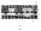
- FIG. 38 illustrates etch of a narrow pressure port channel, stopping at silicon oxide; oxide etching is continued; stopping at device layer Si.
- Pressure port channel is positioned in such a way that gas flow resistance, R B , between the channel and the enclosure B is high but finite.
- FIG. 39 illustrates bringing the pressure inside enclosure B to the desired level by applying appropriate pressure differential between the wafer stack and the ambient.
- FIG. 40 illustrates sealing the pressure port channel by depositing sealing material, for example, polysilicon or metal; P B is determined by differential pressure, flow resistance R B and seal pressure P seal .
- sealing material for example, polysilicon or metal
- FIG. 41 illustrates another embodiment of the solution described in FIG. 34 .
- the vertical pressure port channel leads directly to the enclosure B.
- FIG. 42 illustrates sealing the pressure port channel by depositing sealing material, for example, polysilicon or metal; in this embodiment enclosure B pressure P B is equal to seal pressure P seal .
- sealing material for example, polysilicon or metal
- FIG. 43 illustrates another embodiment of the solution described in FIG. 34 .
- the pressure port channel leading to the enclosure B is horizontal and is formed by stand-off features of standard NF processes, or by the absence of Ge layer resulting in no eutectic bond.
- P B is equal to P seal .
- FIG. 44 illustrates a top view of embodiment shown in FIG. 43 , in which enclosure B is exposed to the environment through a side-channel formed by stand-off features of standard NF process, or by the absence of Ge layer resulting in no eutectic bond.
- P B is equal to P seal .
- the present invention relates generally to the fabrication of MEMS devices, and more particularly to providing for two or more cavities with different pressures, or requiring different ambient gasses for operation, on the same chip involving a wafer bonding technique.
- the present invention provides for multiple approaches and methods for creating multiple pressure levels in multiple cavities fabricated on the chip by a process such as an NF process.
- the present invention relates generally to MEMS devices and more particularly relates to MEMS devices that are hermetically sealed.
- MEMS devices that are hermetically sealed.
- four methods which are described below and include: A. Secondary sealed enclosure, B. Multiple ambient enclosures created during wafer bonding (with four approaches), C. Internal gas reservoir, and D. Controlled leak/breach (with three approaches).
- Table 1 presents a generalized summary of the advantages of each method and approach.
- FIG. 1 provides for the fabrication of CMOS-MEMS integrated devices using eutectic wafer bonding to create a sealed enclosure between the MEMS and CMOS wafers as well as to make electrical interconnection between the MEMS device and CMOS circuits.
- a method and system in accordance with the present invention provides for the integration of two or more MEMS devices that require different operating pressures or ambient gasses in operation.
- MEMS resonators which typically require a low and stable pressure may be integrated with inertial sensors such as accelerometers or gyroscopes which require a higher pressure to operate.
- a method and system in accordance with the present invention provides for the integration of multiple devices, such as one or more of one or more MEMS resonators, MEMS sensors, MEMS inertial sensors, and/or other MEMS structures, and so on, as available to one skilled in the art, into an integrated CMOS-MEMS process in order to create multiple ambients for multiple devices. It further provides a means for electrical interconnection of the enclosed MEMS devices and, optionally, the capping layer(s) to MEMS structures outside of the enclosure and to a CMOS wafer.
- a method in accordance with the present invention in one or more embodiments, in one or more approaches, provides for a method for integrating a second sealed enclosure alongside the main sealed enclosure.
- CMOS-MEMS complementary metal-oxide-semiconductor
- the CMOS wafer may be replaced by any suitable capping wafer or substrate.
- a MEMS structure comprises a MEMS wafer.
- a MEMS wafer includes a handle wafer with cavities bonded to a device wafer through a dielectric layer disposed between the handle and device wafers. The bonding of the device wafer and subsequent thinning of the device wafer produces an intermediate stage of the process referred to as an Engineered Silicon on Insulator wafer where cavities in the handle wafer are sealed by a layer of the device wafer.
- the MEMS wafer also includes a moveable portion of the device wafer suspended over a cavity in the handle wafer.
- the MEMS wafer includes standoffs that are defined by selectively removing areas of the device wafer to product protrusions or standoffs of the device layer.
- a germanium material is then disposed over these standoffs and will be used to adhere a CMOS wafer to the MEMS wafer through aluminum to germanium bonding.
- the MEMS wafer Prior to bonding the MEMS wafer also includes a moveable portion of the device wafer suspended over a cavity in the handle wafer. These portions are typically defined by a lithographic masking and etch steps.
- a method in accordance with the present invention provides a series of approaches for methods for producing two or more cavities with different pressures or ambient on the same chip using wafer bonding.
- FIGS. 2-14 set forth a process for integrating a secondary sealed enclosure in addition to the main sealed enclosure, in accordance with one or more embodiments, whereby the process creates a first enclosure prior to bonding using additional deposition steps and a second enclosure using wafer bonding.
- FIG. 2 sets forth a process 200 for integrating a secondary sealed enclosure in addition to the main sealed enclosure, in accordance with one or more embodiments.
- the wafer is processed in accordance with the standard NF process up to and including Stand-off Etch at 210 .
- the starting wafer provides a silicon device layer 302 bonded to a silicon handle wafer 303 through an insulating layer 304 situated between the device layer and handle wafer, and stand-offs 306 formed from the device layer.
- the silicon device layer 302 is patterned and etched to define the MEMS devices to be sealed in the separate enclosure at 220 ( FIG. 4 ).
- the openings 312 in the device layer are sufficiently narrow or are further processed to be so in preparation to be sealed by a conformal or partially conformal deposition of the sacrificial layer 314 deposited in the following step.
- a sacrificial spacer layer 314 e.g., silicon oxide, etc.
- plug openings 312 created in the device layer from the previous silicon etch step FIG. 5 .
- all openings would be fully plugged to optimize the results sought.
- a first capping layer 316 is deposited on top of the sacrificial layer at 240 .
- the sacrificial layer comprises an electrically conductive material (e.g., poly-crystalline silicon, epitaxial silicon, other similar semi-conductor(s), metal, etc.) or an electrically insulating layer (e.g. silicon nitride, aluminum oxide, aluminum nitride, silicon oxide, etc.).
- the first capping layer 316 is patterned and etched stopping on the underlying sacrificial layer 314 so as to create openings 318 over the enclosure to be sealed, with such openings being preferably sufficiently narrow so as to be sealable by a conformal or partially conformal deposition of the second capping layer 320 to be deposited in a following step ( FIG. 7 ). Further, this step may optionally also provide for the creation of additional openings in the capping layer distal from the enclosure to be sealed in order to provide for, in combination with the following sacrificial layer etch, electrical contact vias between the device layer 302 and the second capping layer 320 , to be deposited in a following step.
- the wafer at 260 is then subjected to an isotropic etchant that selectively removes the sacrificial layer 314 while preserving the first capping layer 316 and the silicon device layer 302 .
- this etching process of a method and system in accordance with the present invention will effectively open the cavity between the first capping layer and the silicon device layer and will also remove the sacrificial layer over the contact vias as defined by the prior step.
- a second capping layer 320 is deposited to a predetermined and sufficient thickness to preferably seal the openings 318 in the first capping layer 316 over the enclosure, thereby creating a sealed enclosure 332 ( FIG. 9 ).
- the second capping layer 320 may also comprise an electrically conductive or electrically insulating material.
- the deposition of this step may be performed in a low pressure environment to seal a low pressure inside the enclosure 332 or sealed in a preferred or desired ambient (i.e., gas) compatible with the deposition.
- a hydrogen rich ambient may be sealed in the enclosure with the hydrogen later diffused out of the enclosure by a high temperature vacuum bake. It will be recognized by those skilled in the art that the invention is not so limited to the exemplars herein but instead a method and system in accordance with the present invention may have many beneficial variations.
- both the first and second capping layers 316 and 320 are patterned and etched stopping on the underlying sacrificial layer 314 .
- the sacrificial layer 314 is then removed at 280 using a wet or dry etch, stopping on the silicon device layer ( FIG. 11 ).
- the NF process is continued for the remaining standard operation (i.e., normally with Germanium ( 322 ) deposition, pattern and etch at 290 ; silicon device layer 302 pattern and etch in 295 , followed by eutectic bonding to a CMOS wafer 326 in step 297 ) shown in FIG. 14 .
- the result of the process is a MEMS device 299 having an integrated second sealed enclosure in addition to the main sealed enclosure.
- the second sealed enclosure may reside inside or outside of the main sealed enclosure.
- FIGS. 15-27 set forth a process, in various methods, for integrating a second sealed enclosure in addition to the main sealed enclosure, in accordance with one or more embodiments, whereby the process creates two or more enclosures with different pressures or ambients during the wafer bonding process, which allows for multiple pressure and/or gas composition on a single device using a single bond step.
- FIG. 15 sets forth a process 400 for integrating two sealed enclosures with different gas compositions and/or pressures, in accordance with one or more embodiments.
- a method is provided to create two or more cavities with different pressures or ambients during the wafer bonding process, which allows for multiple pressure and/or gas composition through the single bond step.
- multiple methods may be further adapted in one or more embodiments to benefit from the process of a method and system in accordance with the present invention.
- Various embodiments may include a variety of options and approaches, such as but not limited to: multiple material systems; controlled solder flow; outgassing/gettering; and, multiple height seal rings, for instance.
- FIGS. 15-18 may refer to an approach involving multiple material systems.
- seal-rings defining different enclosures use different material systems, where the different material systems have different bonding temperatures.
- Different material systems may differ in their composition, doping, grain structure, or surface topology.
- different material systems would have different reflow temperatures.
- different frit compositions would be used for the different cavities, each composition having a different reflow temperature.
- the bonding cycle in such a system would consist of two temperature stages.
- two wafers ( 502 , 504 ) are brought together in a bond chamber and first pressure or ambient desired for the first device (Ambient A) is established in the bonding chamber and the wafers are first raised to a temperature sufficient to reflow the solder of the first material system 506 but not that of the second material system 510 thereby sealing the first device enclosure 508 a while keeping the second device enclosure 508 b unsealed, at 410 .
- the second cavity 508 b may likely leak to the bond chamber ambient or pressure by virtue of the surface roughness of the seal-ring surface between the two wafers, at 420 .
- pressure or ambient desired for the second device is then established in the bonding chamber and the wafer temperature is raised further at 440 so as to reflow the solder of the second material system 510 thereby sealing the second device enclosure 508 b at 450 , whereby multiple cavities with multiple gas compositions and/or pressures are created during wafer bonding at 460 , in accordance with a method and system in accordance with the present invention.
- FIGS. 19-22 may refer to an approach involving controlled solder flow.
- the two or more enclosures use solder seal-rings 610 a , 610 b with identical material systems.
- some enclosures may have a small gap 620 in the seal-ring solder. Therefore, as the wafer temperature is raised, the seal-ring 610 a without a gap will typically seal first, then as the temperature is raised further or additional force is applied, or simply due to additional time, solder flow across the gaps will seal the enclosures with seal-rings 610 b containing gaps 620 . Therefore, for a method and system in accordance with the present invention, by controlling the bond chamber pressure or ambient between the two sealing events, the pressure or ambient of the different devices can be independently controlled.
- the first enclosure 630 a will contain a full seal-ring 610 a
- the second enclosure 630 b will contain seal-ring 610 b with a small gap 620 .
- a pressure or ambient required by the second enclosure 630 b (Ambient B) thereafter is established in the bond chamber and the wafer temperature is raised further to increase the amount of reacted solder, producing sufficient solder volume and flow to cross the gap 620 in the seal-ring of the second enclosure 630 b thereby sealing the second enclosure.
- FIGS. 23-24 may refer to an approach involving outgassing/gettering.
- a substance that either outgases or absorbs (getters) gas at high temperature is included in one or more of the enclosures.
- the two wafers 702 , 704 are then sealed using any valid high-temperature approach including solder reflow, glass frit, anodic bonding, or epoxy bonding.
- the included substance will either outgas, thereby creating a higher pressure in its enclosure, or serve as a getter thereby creating a lower pressure in its enclosure.
- FIG. 23 illustrates that a single pressure is established in the bond chamber during reflow of seal-rings of both enclosure 708 a and enclosure 708 b .
- enclosure 708 b contains a gettering element 706 that, at elevated temperature, absorbs at least one of the gasses present in the enclosure to decrease enclosure pressure.
- FIGS. 23-24 may refer to an approach involving outgassing/gettering. It can be understood that the exemplary aspects depicted in FIGS. 23-24 are shown in simplified form, without other details depicted, for example, regarding FIGS. 3-14 , for the purposes of illustration of sealed enclosures having different cavity pressures as a result of inclusion of a Bettering or an outgassing substance in one or more of the sealed enclosures with a MEMS structure, and not limitation. As such, it can be further understood one or more of the sealed enclosures depicted in FIGS.
- MEMS structure such as MEMS resonators, MEMS sensors, MEMS inertial sensors, and/or other MEMS structures, and so on, as available to one skilled in the art.
- a substance that either outgases or absorbs (getters) gas at high temperature is included in one or more of the enclosures.
- the two wafers 702 , 704 are then sealed using any valid high-temperature approach including solder reflow, glass frit, anodic bonding, or epoxy bonding.
- the included substance will either outgas, thereby creating a higher pressure in its enclosure, or serve as a getter thereby creating a lower pressure in its enclosure.
- the environment of a sealed enclosure for an exemplary MEMS device can have a higher cavity pressure (where a material is included in the sealed enclosure that can desorb (outgas) gas molecules) as a result of desorption of gas molecules than another of the sealed enclosures that does not include an out-gassing substance. It can be further understood that, after sealing, the environment of the sealed enclosure for an exemplary MEMS device can have a lower cavity pressure (where a material is included in the sealed enclosure that can absorb (getter) gas molecules) as a result of absorption of gas molecules than another of the sealed enclosures that does not include a gettering substance.
- FIGS. 25-27 may refer to an approach involving multiple height seal rings.
- seal-ring solder materials for the two or more enclosures are of different heights such that, when wafers 802 and 804 are brought together in the bond chamber 810 , only the tallest seal-ring will initially be in physical contact.
- a first gas pressure and composition (Ambient A) is established in the bond chamber, and then a force is applied pushing the two wafers together.
- the solder used may be a two component solder, with one component disposed on the bottom wafer and the other component on the top wafer, such that reflow at a particular temperature only occurs if the two components are in contact.
- FIGS. 28-33 set forth a process flow chart for integrating a secondary sealed enclosure (reservoir under a pressure in Ambient I) in addition to a main sealed enclosure (under another pressure in Ambient II), in accordance with one or more embodiments, whereby the process exposes one main enclosure open to the associated reservoir cavity after wafer bonding.
- the final enclosed pressures in Device A or B depend on both pressures of Ambient I and II.
- the Internal Gas Reservoir process method achieves well controlled multiple pressures and/or gas compositions.
- a CMOS-MEMS wafer comprises a standard CMOS wafer with an aluminum top metallization layer eutecticly bonded to a MEMS wafer.
- FIG. 28 sets forth a process 900 for the Internal Gas reservoir method.
- a silicon handle wafer 1002 with etched reservoirs 1008 , 1010 and main cavities 1008 , 1010 and a device wafer 1004 are bonded and sealed hermetically during wafer fusion bonding at 910 providing an Engineered SOI (ESOI) wafer 1011 .
- ESOI Engineered SOI
- the MEMS wafer is further processed through stand-off 1005 formation in 920 .
- the device layer under the reservoirs 1012 and 1014 may be thinned, providing membranes 1007 , to simplify breaching the reservoirs in the following steps.
- all cavities 1008 , 1010 and gas reservoirs 1012 , 1014 in the ESOI wafer have the same reservoir pressure P res which was set during fusion bonding of handle and device wafers, in Ambient I.
- P res reservoir pressure
- the MEMS wafer is further processed through germanium 1016 deposition, pattern, and etch, and device wafer 1004 pattern and etch in 930 , providing a completed MEMS wafer 1021 .
- the cavities 1008 and 1010 are opened to the external environment. From FIGS.
- the MEMS wafer 1021 is eutecticly bonded to a CMOS wafer 1020 under bonding pressure P bond in Ambient II at 940 , forming sealed device enclosures 1052 and 1054 .
- the silicon membranes between the internal gas reservoirs 1012 , 1014 and the associated device enclosures are opened at 950 .
- the silicon membranes may be opened at either location 1050 or 1051 using Laser Stealth Dicing (LSD), externally applied mechanical stress, or another valid method.
- LSD Laser Stealth Dicing
- a CMOS-MEMS wafer with MEMS device enclosures A and B of different final equilibrant pressures is provided.
- final equilibrium pressures of enclosures for device A and B will be P A and P B , respectively, determined by P res , P bond and volumes V res and V Cav of corresponding internal gas reservoirs and devices.
- the Laser Stealth Dicing (LSD) technique is used to Laser cut (or break) the thin isolation silicon membranes between the respective internal gas reservoir and main MEMS device enclosures within the die.
- the membranes could be parallel or normal to the CMOS wafer surface by design.
- FIGS. 34-44 set forth three approaches for a method for integrating at least two MEMS devices in hermetically sealed enclosures of different pressures or gas compositions on the same die.
- the Controlled Leak/Breach method in accordance with the present invention allows for multiple pressure and/or gas composition via a single bond step and post-bonding process steps.
- a starting material (Standard Nasiri-Fabrication process through Stand-Off etch) is set forth.
- a device layer pattern and DRIE occurs at 1120 , then a bonding to the CMOS wafer at 1130 .
- a narrow pressure port channel is etched.
- the pressure inside Enclosure B is brought to a desired level by applying an appropriate pressure differential between the wafer stack and the ambient.
- the pressure port channel is sealed by depositing a sealing material.
- a two cavity (or enclosure) MEMS device is provided.
- FIG. 35 illustrates the cross-section view of a starting material having a handle wafer 1202 with etched cavities 1210 and 1220 and a device wafer 1204 , standoff 1205 , and oxide thin film 1206 .
- FIG. 36 illustrates a number of process steps including Ge deposition/pattern/etch 1216 and a device actuator pattern and etch 1290 , providing MEMS wafer 1220 .
- FIG. 37 illustrates a step of bonding the MEMS wafer 1220 to a CMOS wafer 1208 by an eutectic bond of Ge 1216 and Al 1224 ; at this point both enclosures A and B ( 1290 and 1291 ) have the same pressure, P bond .
- FIG. 38 illustrates a step of etching a narrow pressure port channel 1211 proximate to enclosure B 1291 , stopping at silicon oxide 1204 ; oxide etching then continued; stopping at device Si 1206 .
- Pressure port channel is positioned in such a way that gas flow resistance 1212 , R B between the channel 1211 and the enclosure B 1291 is high but finite.
- FIG. 39 illustrates a step to bring the pressure inside enclosure B 1291 to the desired level by applying appropriate pressure differential between the internal pressure of enclosure B 1291 and the outside ambient 1218 .
- the ambient pressure 1218 P amb is preferably brought down to such a level that controlled gas leakage through the flow resistance R B brings the pressure in enclosure B 1291 to a desired level.
- Controlled gas leakage can be either into or out of enclosure B 1291 depending on the sign of the pressure differential, therefore final pressure in enclosure B 1291 P B can be either lower or higher then pressure P A in enclosure A 1290 , which remains equal to P bond .
- FIG. 40 illustrates a step of sealing the pressure port channel by depositing sealing material 1230 , for example polysilicon, or metal; P B is determined by the differential pressure in step 1150 , flow resistance R B , and the sealing pressure P seal .
- FIG. 40 further illustrates that the pressure P seal at which sealing is performed is typically different from P amb . Therefore, while sealing is taking place, pressure in Enclosure B 1291 will change. However, because the flow resistance R B is relatively high, this change can be relatively small. Thus a method and system in accordance with the present invention may benefit by setting pressure in Enclosure B (P B ) to be substantially different from pressure in Enclosure A (P A ) and from the sealing pressure P seal .
- P B pressure in Enclosure B
- MEMS devices may now have more than two enclosed cavities and more than two pressure port channels.
- Leak resistances R B , R C , etc. are provided by the design and can be controlled as desired to achieve P A P B , P C , etc. as desired. All of the channels, however, are sealed off at once at the same pressure P seal .
- This embodiment provides the added benefit of having enclosure B being substantially isolated and protected during manufacturing steps, such as dicing and sawing, from particles and moisture present at these steps.
- FIGS. 41-42 set forth a second approach for a method for integrating at least two MEMS devices in hermetically sealed enclosures of different pressure or gas composition in a same die.
- FIG. 41 illustrates another embodiment of the solution described in Controlled Leak/Breach method.
- the vertical pressure port channel 1316 leads directly to the enclosure B 1391 .
- P B is equal to P seal .
- This embodiment provides additional benefits of providing an implementable solution for creating multiple cavities with two levels of pressure.
- FIG. 42 illustrates sealing the pressure port channel 1316 by depositing sealing material 1392 , for example, polysilicon or metal; in this embodiment P B is equal to P seal .
- FIGS. 43-45 set forth a third approach for a method for integrating at least two MEMS devices in hermetically sealed enclosures of different pressure or gas composition in a same die.
- the Controlled Leak/Breach method in accordance with the present invention allows for multiple pressure and/or gas composition via the single bond step and post-bonding steps, where the pressure port channel 1410 leading to the enclosure B 1491 is horizontal and formed by a stand-off feature of the standard NF process, or by absence of Ge layer resulting in no bond.
- the side channel 1410 is sealed by depositing a sealing material 1430 , for example polysilicon or metal.
- P B is equal to P seal .
- FIG. 46 illustrates a top view of the embodiment shown in FIG. 45 , in which enclosure B 1491 is exposed to the environment through a side-channel 1410 formed by stand-off features of standard NF process, or by absence of Ge layer resulting in no bond; in this embodiment P B is equal to P seal .
Landscapes
- Engineering & Computer Science (AREA)
- Microelectronics & Electronic Packaging (AREA)
- Manufacturing & Machinery (AREA)
- Computer Hardware Design (AREA)
- Micromachines (AREA)
Abstract
A Microelectromechanical systems (MEMS) structure comprises a MEMS wafer. A MEMS wafer includes a handle wafer with cavities bonded to a device wafer through a dielectric layer disposed between the handle and device wafers. The MEMS wafer also includes a moveable portion of the device wafer suspended over a cavity in the handle wafer. Four methods are described to create two or more enclosures having multiple gas pressure or compositions on a single substrate including, each enclosure containing a moveable portion. The methods include: A. Forming a secondary sealed enclosure, B. Creating multiple ambient enclosures during wafer bonding, C. Creating and breaching an internal gas reservoir, and D. Forming and subsequently sealing a controlled leak/breach into the enclosure.
Description
This application claims the benefit of U.S. Provisional Patent Application No. 61/501,652, filed on Jun. 27, 2011, entitled “MEMS DEVICES, INTEGRATED MEMS-CMOS,” which is incorporated herein by reference in its entirety.
The present invention relates generally to MEMS (Microelectromechanical systems) devices and more particularly relates to MEMS devices that are hermetically sealed.
MEMS technology has advanced to provide integrated packaging of the MEMS devices or sensors. This integration advancement typically refers to processes or methods at which the packaging of the MEMS device is in the form of a protective cap which hermetically seals the device from the outside environment. Furthermore it protects the MEMS device from subsequent assembly operations such as saw cutting for singulation. The processes and methods are performed at a wafer level rather than a die level. The wafer level integration offers a more efficient and cost effective manner to package the MEMS devices. One such wafer level packaging technique is the Nasiri-Fabrication platform depicted in FIG. 1 . In FIG. 1 , the Nasiri-Fabrication (NF) platform uses a patented wafer-to-wafer bonding process 100 that directly integrates pre-fabricated MEMS wafers 110 to off-the-shelf complementary metal-oxide semiconductor (CMOS) wafers 120 at the wafer level. The process also simultaneously provides electric contact and hermetic sealing 130 of all MEMS elements at the wafer level.
Using the process, which uses six masks, engineered silicon on insulator (ESOI) wafer 150 is formed starting with a standard silicon handle wafer etched with targets for backside alignment (mask 1); followed by oxidation and cavity etch (mask 2). A second wafer is fusion bonded to the handle wafer and subsequently thinned to define the device layer thickness. The MEMS wafer 110 is completed by etching the device layer to form standoffs (mask 3) that define the seal ring, the electrical contacts to CMOS, and the vertical gap between the CMOS and MEMS; depositing and patterning a germanium layer (mask 4) over standoffs; and patterning (mask 5) and deep reactive ion etching the device layer to form the mechanical structure 135.
Continuing, a standard CMOS wafer is fabricated, with optional etched cavities (mask 6), if needed for larger clearance under moving MEMS structures. The MEMS wafer is bonded to the CMOS wafer using AIGe eutectic bonding between the Al on the CMOS and the Ge on the MEMS wafer at 140, for example. After bonding, a portion of the MEMS wafer is removed by conventional dicing saw cuts to expose the CMOS wire bond pads 125.
While the Nasiri-Fabrication process is ideally suited for operational environments as is proven by the success of the process today, it is often desirable to have different devices sealed at different pressures or different gas compositions when integrating multiple MEMS devices on the same chip. It will be recognized by those skilled in the art that such a need may arise where, for instance, different devices are sought to be optimized for different pressures or where different devices may require different ambient gasses or pressures (hereby referred to as ambient or ambients) to operate.
Other attempts to provide for a sealed element, such as that of U.S. Pat. No. 5,285,131 disclose steps to create a MEMS element sealed in an enclosure using two capping layers and a sacrificial layer. Similarly, U.S. Pat. Nos. 6,936,491 and 7,075,160 further disclose the addition of an insulated via to make electrical contact to the underlying silicon (the latter method not taught or required for this invention).
Unfortunately, these attempts do not overcome the challenges encountered when integrating multiple MEMS devices on a single chip, where it is often desirable to have different devices sealed at different pressures involving minimal processing steps, achieving a more predictable outcome through improved control, and having reduced requirements for the commodity of space or “real estate.” Similarly, what is desired is a system and method that overcomes these challenges and provides for two or more cavities with different pressures or requiring different ambient gasses for operation on the same chip involving a wafer bonding technique. Further what is needed is a system and method providing for the integration of such devices into an integrated CMOS-MEMS to create multi-ambient devices.
The present invention fulfills these needs and has been developed in response to the present state of the art, and in particular, in response to the problems and needs in the art that have not yet been fully solved by currently available technologies.
One embodiment of the present invention (Approach A) provides for two sealed enclosures through two different enclosure methods. One enclosure is achieved through conventional Nasiri Fabrication wafer bonding and a secondary enclosure is formed through a wafer encapsulation method comprising of deposited structural and sacrificial materials to construct a shell like enclosure. This embodiment comprises: a MEMS wafer including: a handle wafer with cavities bonded to a device wafer through a dielectric layer disposed between the handle and device wafers; a moveable portion of the device wafer suspended over a cavity in the handle wafer; a capping layer attached to the device wafer and separated by an air gap from the moveable portion of the device wafer, to form a first enclosure with a first ambient pressure. A second enclosure with a second ambient pressure is formed through CMOS-MEMS wafer bonding on another movable portion of the device wafer. The second enclosure can but is not restricted to enclose the first enclosure.
Another embodiment of the present invention (Approach B) provides for a method for integrating two sealed enclosures for each of two MEMS devices each having a silicon device layer, whereby the process creates a first enclosure and a second enclosure using wafer bonding, comprising the steps of: using a standard Nasiri-Fabrication (NF) process up to and including Stand-off Etch, processing a wafer; patterning and etching the silicon device layer and finally integrating to CMOS through a wafer bonding process. The environment of each enclosure, including its gas species and pressure, is controlled during the wafer bonding process where each enclosure is sealed. Several methods are considered including methods where the sealing is performed at different times during the wafer bonding process. A second approach to establish multiple pressures during the wafer bonding involves a method where a material is included in one of the enclosures that can absorb (getter) or desorb (outgas) gas molecules which can affect the pressure. In the case where the material has absorptive properties (getter) the pressure would decrease and in the case of desorptive properties (outgas) the pressure will increase. Accordingly, it can be understood that, with the second approach, after sealing, the environment of a sealed enclosure for an exemplary MEMS device can have a higher cavity pressure (where a material is included in the sealed enclosure that can desorb (outgas) gas molecules) as a result of desorption of gas molecules than another of the sealed enclosures that does not include an out-gassing substance. It can be further understood that, after sealing, the environment of the sealed enclosure for an exemplary MEMS device can have a lower cavity pressure (where a material is included in the sealed enclosure that can absorb (getter) gas molecules) as a result of absorption of gas molecules than another of the sealed enclosures that does not include a gettering substance.
Another embodiment of the invention (Approach C) provides for an internal gas reservoir for one of the sealed enclosures to tap into after wafer bonding. The internal gas reservoir comprises a sealed cavity during the Engineered SOI wafer formation of the Nasiri fabrication process. The pressure of the sealed cavity and the desired ambient gas can be sealed into the gas reservoir cavities during the fusion bonding step of the Nasiri Fabrication process of forming the engineered SOI wafer. This sealed cavity or reservoir is then connected to one of the sealed enclosures to control the enclosure's final pressure or gas composition. The connection method is similar to an electrical fuse where in this embodiment a flow channel fuse is opened to connect the sealed enclosure to the reservoir. The method can include applying thermal energy to create the opening such as focused laser ablation or Joule heating. The laser ablation may include a focused beam where the energy is concentrated to a certain depth.
A further embodiment of the present invention (Approach D) provides for a method for integrating a secondary sealed enclosure in parallel with a main sealed enclosure. The pressure and ambient gas in the main enclosure is determined during wafer bonding process and the pressure in the secondary sealed enclosure is determined by a post bond sealing of a designed breach or channel of the second enclosure. The post bond process will expose the enclosure to the appropriate pressure and then seal it at that pressure. Each enclosure initially has approximately the same pressure, comprising the steps of: processing a wafer using the Nasiri Fabrication process to create one or more pressure ports. A controlled breach is then created in the second enclosure, and the wafer is then sealed in an ambient that is desirable for the second enclosure. The sealing process operating pressure defines the pressure of the second enclosure. An extension of this embodiment is to design the port to comprise a channel having a gas flow resistance between the port and a secondary enclosure. The flow resistance provides a slow conductance path for a gas to flow into or out of the enclosure. The conductance is then a function of the pressure differential which can be applied in a step separate from the final sealing step. The resistance path is designed to be conductive or flowable for a larger pressure differential but can be relatively non-flowing at pressure differentials less than one atmosphere. A high pressure source is envisioned to provide the necessary pressure differential to push desired gas into or out of the secondary enclosure. Alternately, a sufficiently long exposure at a lower pressure differential may be sufficient to achieve the desired pressure inside the second enclosure. This provides a greater flexibility of pressure values for the second enclosure where the pressure and ambient gas are not dependent on the sealing process.
Other aspects and advantages of the present invention will become apparent from the following detailed description, taken in conjunction with the accompanying drawings, illustrating by way of example the principles of the invention.
The present invention relates generally to the fabrication of MEMS devices, and more particularly to providing for two or more cavities with different pressures, or requiring different ambient gasses for operation, on the same chip involving a wafer bonding technique. The present invention provides for multiple approaches and methods for creating multiple pressure levels in multiple cavities fabricated on the chip by a process such as an NF process.
Approach Comparisons
The present invention relates generally to MEMS devices and more particularly relates to MEMS devices that are hermetically sealed. Presented are four methods, which are described below and include: A. Secondary sealed enclosure, B. Multiple ambient enclosures created during wafer bonding (with four approaches), C. Internal gas reservoir, and D. Controlled leak/breach (with three approaches). Table 1 presents a generalized summary of the advantages of each method and approach.
| TABLE 1 |
| Comparison of several approaches |
| Approach | Advantage | General Comment |
| A: Secondary | One regular pressure | creates a first enclosure prior to |
| sealed | and one very low | bonding using additional |
| enclosure | pressure | deposition steps and the second |
| enclosure using wafer bonding | ||
| B: Multiple | Simplest approach | creates two or more cavities with |
| ambient | different pressures or ambients | |
| enclosures | during the wafer bonding process | |
| C: Internal gas | More control, | creates a secondary pressure |
| reservoir | multiple pressures/ | cavity by including a gas reservoir |
| multiple gasses; | near the main enclosure which is | |
| Fewer additional | breached after wafer bonding. | |
| process steps | ||
| D: Controlled | multiple pressures/ | keeps one cavity open to the |
| leak/breach | multiple gasses | environment after wafer bonding |
| (or alternately opens a channel | ||
| into that cavity after wafer | ||
| bonding) which is later sealed at | ||
| the desired secondary pressure or | ||
| ambient | ||
The process described in FIG. 1 provides for the fabrication of CMOS-MEMS integrated devices using eutectic wafer bonding to create a sealed enclosure between the MEMS and CMOS wafers as well as to make electrical interconnection between the MEMS device and CMOS circuits. A method and system in accordance with the present invention provides for the integration of two or more MEMS devices that require different operating pressures or ambient gasses in operation. For example, MEMS resonators which typically require a low and stable pressure may be integrated with inertial sensors such as accelerometers or gyroscopes which require a higher pressure to operate. In one or more embodiments, a method and system in accordance with the present invention provides for the integration of multiple devices, such as one or more of one or more MEMS resonators, MEMS sensors, MEMS inertial sensors, and/or other MEMS structures, and so on, as available to one skilled in the art, into an integrated CMOS-MEMS process in order to create multiple ambients for multiple devices. It further provides a means for electrical interconnection of the enclosed MEMS devices and, optionally, the capping layer(s) to MEMS structures outside of the enclosure and to a CMOS wafer. A method in accordance with the present invention, in one or more embodiments, in one or more approaches, provides for a method for integrating a second sealed enclosure alongside the main sealed enclosure. Below are provided a variety of approaches available with a method and system in accordance with the present invention, in one or more embodiments, providing for the integration of such devices into an integrated CMOS-MEMS to create multi-ambient devices. In the described embodiments, the CMOS wafer may be replaced by any suitable capping wafer or substrate.
For each of the approaches, it will be appreciated that a MEMS structure comprises a MEMS wafer. A MEMS wafer includes a handle wafer with cavities bonded to a device wafer through a dielectric layer disposed between the handle and device wafers. The bonding of the device wafer and subsequent thinning of the device wafer produces an intermediate stage of the process referred to as an Engineered Silicon on Insulator wafer where cavities in the handle wafer are sealed by a layer of the device wafer. The MEMS wafer also includes a moveable portion of the device wafer suspended over a cavity in the handle wafer. The MEMS wafer includes standoffs that are defined by selectively removing areas of the device wafer to product protrusions or standoffs of the device layer. A germanium material is then disposed over these standoffs and will be used to adhere a CMOS wafer to the MEMS wafer through aluminum to germanium bonding. Prior to bonding the MEMS wafer also includes a moveable portion of the device wafer suspended over a cavity in the handle wafer. These portions are typically defined by a lithographic masking and etch steps.
The following description is presented to enable one of ordinary skill in the art to make and use the invention and is provided in the context of a patent application and its requirements. Various modifications to the preferred embodiment and the generic principles and features described herein will be readily apparent to those skilled in the art. Thus, a method and system in accordance with the present invention is not intended to be limited to the embodiment shown but is to be accorded the widest scope consistent with the principles and features described herein.
A method in accordance with the present invention provides a series of approaches for methods for producing two or more cavities with different pressures or ambient on the same chip using wafer bonding.
A. Secondary Sealed Enclosure Approach
From FIG. 2 and FIG. 3 , the wafer is processed in accordance with the standard NF process up to and including Stand-off Etch at 210. The starting wafer provides a silicon device layer 302 bonded to a silicon handle wafer 303 through an insulating layer 304 situated between the device layer and handle wafer, and stand-offs 306 formed from the device layer. Once the wafer has been processed up to and including Stand-off Etch, the silicon device layer 302 is patterned and etched to define the MEMS devices to be sealed in the separate enclosure at 220 (FIG. 4 ). Preferably at 220, the openings 312 in the device layer are sufficiently narrow or are further processed to be so in preparation to be sealed by a conformal or partially conformal deposition of the sacrificial layer 314 deposited in the following step. At 230 a sacrificial spacer layer 314 (e.g., silicon oxide, etc.) is deposited onto the wafer to a predetermined and sufficient thickness so as to plug (i.e., pinch-off) openings 312 created in the device layer from the previous silicon etch step (FIG. 5 ). Preferably, all openings would be fully plugged to optimize the results sought.
Further from FIGS. 2 and 6 , a first capping layer 316 is deposited on top of the sacrificial layer at 240. In one or more preferred embodiments, the sacrificial layer comprises an electrically conductive material (e.g., poly-crystalline silicon, epitaxial silicon, other similar semi-conductor(s), metal, etc.) or an electrically insulating layer (e.g. silicon nitride, aluminum oxide, aluminum nitride, silicon oxide, etc.). At 250, the first capping layer 316 is patterned and etched stopping on the underlying sacrificial layer 314 so as to create openings 318 over the enclosure to be sealed, with such openings being preferably sufficiently narrow so as to be sealable by a conformal or partially conformal deposition of the second capping layer 320 to be deposited in a following step (FIG. 7 ). Further, this step may optionally also provide for the creation of additional openings in the capping layer distal from the enclosure to be sealed in order to provide for, in combination with the following sacrificial layer etch, electrical contact vias between the device layer 302 and the second capping layer 320, to be deposited in a following step.
From FIG. 2 and FIG. 8 , the wafer at 260 is then subjected to an isotropic etchant that selectively removes the sacrificial layer 314 while preserving the first capping layer 316 and the silicon device layer 302. From step 260, this etching process of a method and system in accordance with the present invention will effectively open the cavity between the first capping layer and the silicon device layer and will also remove the sacrificial layer over the contact vias as defined by the prior step. At 270, a second capping layer 320 is deposited to a predetermined and sufficient thickness to preferably seal the openings 318 in the first capping layer 316 over the enclosure, thereby creating a sealed enclosure 332 (FIG. 9 ). Preferably, in one or more embodiments, all openings would be fully plugged to optimize the results sought. The second capping layer 320 may also comprise an electrically conductive or electrically insulating material. Optionally, the deposition of this step may be performed in a low pressure environment to seal a low pressure inside the enclosure 332 or sealed in a preferred or desired ambient (i.e., gas) compatible with the deposition. In one embodiment, it is envisioned that a hydrogen rich ambient may be sealed in the enclosure with the hydrogen later diffused out of the enclosure by a high temperature vacuum bake. It will be recognized by those skilled in the art that the invention is not so limited to the exemplars herein but instead a method and system in accordance with the present invention may have many beneficial variations.
From FIG. 2 and FIG. 10 , at 275, both the first and second capping layers 316 and 320 are patterned and etched stopping on the underlying sacrificial layer 314. The sacrificial layer 314 is then removed at 280 using a wet or dry etch, stopping on the silicon device layer (FIG. 11 ). Once the sacrificial layer 314 is removed, the NF process is continued for the remaining standard operation (i.e., normally with Germanium (322) deposition, pattern and etch at 290; silicon device layer 302 pattern and etch in 295, followed by eutectic bonding to a CMOS wafer 326 in step 297) shown in FIG. 14 . The result of the process is a MEMS device 299 having an integrated second sealed enclosure in addition to the main sealed enclosure. In an embodiment, the second sealed enclosure may reside inside or outside of the main sealed enclosure.
B. Multiple Ambient Cavities Created During Wafer Bonding
B1—Multiple Material Systems
From FIGS. 15-18 , two wafers (502, 504) are brought together in a bond chamber and first pressure or ambient desired for the first device (Ambient A) is established in the bonding chamber and the wafers are first raised to a temperature sufficient to reflow the solder of the first material system 506 but not that of the second material system 510 thereby sealing the first device enclosure 508 a while keeping the second device enclosure 508 b unsealed, at 410. From step 410, the second cavity 508 b may likely leak to the bond chamber ambient or pressure by virtue of the surface roughness of the seal-ring surface between the two wafers, at 420. Thereafter, at 430, pressure or ambient desired for the second device (Ambient B) is then established in the bonding chamber and the wafer temperature is raised further at 440 so as to reflow the solder of the second material system 510 thereby sealing the second device enclosure 508 b at 450, whereby multiple cavities with multiple gas compositions and/or pressures are created during wafer bonding at 460, in accordance with a method and system in accordance with the present invention.
B2—Controlled Solder Flow
By way of example, adapting the approach of FIG. 15 , for a chip with two enclosures, the first enclosure 630 a will contain a full seal-ring 610 a, while the second enclosure 630 b will contain seal-ring 610 b with a small gap 620. First a pressure or ambient required for the first enclosure 630 a (Ambient A) is established in the bond chamber and the wafer temperature is raised to a level sufficient to reflow the solder only at the interface between the two wafers but induce only minimum solder flow. A pressure or ambient required by the second enclosure 630 b (Ambient B) thereafter is established in the bond chamber and the wafer temperature is raised further to increase the amount of reacted solder, producing sufficient solder volume and flow to cross the gap 620 in the seal-ring of the second enclosure 630 b thereby sealing the second enclosure.
B3—Outgassing/Gettering
B4—Multiple Height Seal-Rings
Approach C: Internal Gas Reservoir
Specifically, with reference to FIG. 32 , it will be appreciated that from a method and system in accordance with the present invention:
P res *Vresa=λresa RT (Eq 1)
P res *Vresa=λresa RT (Eq 1)
where Pres is pressure in reservoir A that has volume Vresa, and λres, is a number on moles of gas in this reservoir. Similar equation can be written for the enclosure A.
P bond *Vcava=λcava RT (Eq 2)
P bond *Vcava=λcava RT (Eq 2)
Combining these two equations gives a formula defining final pressure in joined volume (after breaking silicon membranes by LSD).
Generalizing to reservoir i and enclosure i one gets
which is the final cavity pressure of that particular device with internal gas reservoir of Vresi and device enclosure Vcavi within a die, where i=a, b, c, . . . (or A, B, C, . . . ).
Approach D: Controlled Leak/Breach
From FIG. 34 , at 1110, a starting material (Standard Nasiri-Fabrication process through Stand-Off etch) is set forth. Next, a device layer pattern and DRIE occurs at 1120, then a bonding to the CMOS wafer at 1130. At 1140, a narrow pressure port channel is etched. At 1150, the pressure inside Enclosure B is brought to a desired level by applying an appropriate pressure differential between the wafer stack and the ambient. Then at 1160, the pressure port channel is sealed by depositing a sealing material. At 1199, a two cavity (or enclosure) MEMS device is provided.
By extension, MEMS devices may now have more than two enclosed cavities and more than two pressure port channels. Leak resistances RB, RC, etc. are provided by the design and can be controlled as desired to achieve PA PB, PC, etc. as desired. All of the channels, however, are sealed off at once at the same pressure Pseal.
This embodiment, for this approach, provides the added benefit of having enclosure B being substantially isolated and protected during manufacturing steps, such as dicing and sawing, from particles and moisture present at these steps.
Although the present invention has been described in accordance with the embodiments shown, one of ordinary skill in the art will readily recognize that there could be variations to the embodiments and those variations would be within the spirit and scope of the present invention, such as the inclusion of circuits, electronic devices, control systems, and other electronic and processing equipment. Accordingly, many modifications may be made by one of ordinary skill in the art without departing from the spirit and scope of the appended claims. Many other embodiments of the present invention are also envisioned.
Any theory, mechanism of operation, proof, or finding stated herein is meant to further enhance understanding of the present invention and is not intended to make the present invention in any way dependent upon such theory, mechanism of operation, proof, or finding. It should be understood that while the use of the word preferable, preferably or preferred in the description above indicates that the feature so described may be more desirable, it nonetheless may not be necessary and embodiments lacking the same may be contemplated as within the scope of the invention, that scope being defined by the claims that follow.
Claims (6)
1. A Microelectromechanical Systems (MEMS) device comprising:
a MEMS substrate with cavities bonded to a second substrate, forming a plurality of sealed enclosures, wherein each of the plurality of sealed enclosures is defined by the MEMS substrate, the second substrate, and a seal-ring material, wherein one of the plurality of sealed enclosures includes an inertial sensor;
wherein at least one of plurality of sealed enclosures further includes a non gettering out-gassing substance to desorb one or more gases to increase cavity pressure in the at least one of the plurality of sealed enclosures and at least one other of the plurality of sealed enclosures does not include the non gettering out-gassing substance;
wherein the at least one sealed enclosure with the non gettering out-gassing substance has a higher cavity pressure than the at least one other of the plurality of sealed enclosures without the non gettering out-gassing substance.
2. The MEMS structure of claim 1 , wherein the second substrate comprises a CMOS substrate.
3. The MEMS structure of claim 2 , wherein the CMOS substrate is electrically coupled to the MEMS substrate.
4. The MEMS structure of claim 2 , wherein the non gettering out-gassing substance is on one of the CMOS substrate or the MEMS substrate.
5. The MEMS structure of claim 1 , wherein the second substrate contains an integrated circuit.
6. The MEMS structure of claim 1 , wherein at an elevated temperature, a controlled amount of the one or more gases are desorbed from the non gettering out-gassing substance.
Priority Applications (8)
| Application Number | Priority Date | Filing Date | Title |
|---|---|---|---|
| US13/535,180 US9540230B2 (en) | 2011-06-27 | 2012-06-27 | Methods for CMOS-MEMS integrated devices with multiple sealed cavities maintained at various pressures |
| US14/598,138 US9718679B2 (en) | 2011-06-27 | 2015-01-15 | Integrated heater for gettering or outgassing activation |
| US14/603,185 US9738512B2 (en) | 2012-06-27 | 2015-01-22 | CMOS-MEMS integrated device including multiple cavities at different controlled pressures and methods of manufacture |
| US14/832,786 US9452925B2 (en) | 2011-06-27 | 2015-08-21 | Method of increasing MEMS enclosure pressure using outgassing material |
| US15/265,668 US9731963B2 (en) | 2011-06-27 | 2016-09-14 | Method of increasing MEMS enclosure pressure using outgassing material |
| US15/358,956 US10532926B2 (en) | 2011-06-27 | 2016-11-22 | Methods for CMOS-MEMS integrated devices with multiple sealed cavities maintained at various pressures |
| US15/461,270 US10221065B2 (en) | 2012-06-27 | 2017-03-16 | CMOS-MEMS integrated device including multiple cavities at different controlled pressures and methods of manufacture |
| US16/698,535 US10850973B2 (en) | 2011-06-27 | 2019-11-27 | Methods for CMOS-MEMS integrated devices with multiple sealed cavities maintained at various pressures |
Applications Claiming Priority (2)
| Application Number | Priority Date | Filing Date | Title |
|---|---|---|---|
| US201161501652P | 2011-06-27 | 2011-06-27 | |
| US13/535,180 US9540230B2 (en) | 2011-06-27 | 2012-06-27 | Methods for CMOS-MEMS integrated devices with multiple sealed cavities maintained at various pressures |
Related Child Applications (4)
| Application Number | Title | Priority Date | Filing Date |
|---|---|---|---|
| US14/598,138 Continuation-In-Part US9718679B2 (en) | 2011-06-27 | 2015-01-15 | Integrated heater for gettering or outgassing activation |
| US14/603,185 Continuation-In-Part US9738512B2 (en) | 2012-06-27 | 2015-01-22 | CMOS-MEMS integrated device including multiple cavities at different controlled pressures and methods of manufacture |
| US14/832,786 Continuation-In-Part US9452925B2 (en) | 2011-06-27 | 2015-08-21 | Method of increasing MEMS enclosure pressure using outgassing material |
| US15/358,956 Division US10532926B2 (en) | 2011-06-27 | 2016-11-22 | Methods for CMOS-MEMS integrated devices with multiple sealed cavities maintained at various pressures |
Publications (2)
| Publication Number | Publication Date |
|---|---|
| US20120326248A1 US20120326248A1 (en) | 2012-12-27 |
| US9540230B2 true US9540230B2 (en) | 2017-01-10 |
Family
ID=47361055
Family Applications (3)
| Application Number | Title | Priority Date | Filing Date |
|---|---|---|---|
| US13/535,180 Active US9540230B2 (en) | 2011-06-27 | 2012-06-27 | Methods for CMOS-MEMS integrated devices with multiple sealed cavities maintained at various pressures |
| US15/358,956 Active US10532926B2 (en) | 2011-06-27 | 2016-11-22 | Methods for CMOS-MEMS integrated devices with multiple sealed cavities maintained at various pressures |
| US16/698,535 Active US10850973B2 (en) | 2011-06-27 | 2019-11-27 | Methods for CMOS-MEMS integrated devices with multiple sealed cavities maintained at various pressures |
Family Applications After (2)
| Application Number | Title | Priority Date | Filing Date |
|---|---|---|---|
| US15/358,956 Active US10532926B2 (en) | 2011-06-27 | 2016-11-22 | Methods for CMOS-MEMS integrated devices with multiple sealed cavities maintained at various pressures |
| US16/698,535 Active US10850973B2 (en) | 2011-06-27 | 2019-11-27 | Methods for CMOS-MEMS integrated devices with multiple sealed cavities maintained at various pressures |
Country Status (1)
| Country | Link |
|---|---|
| US (3) | US9540230B2 (en) |
Cited By (1)
| Publication number | Priority date | Publication date | Assignee | Title |
|---|---|---|---|---|
| US11894319B2 (en) | 2020-07-30 | 2024-02-06 | Taiwan Semiconductor Manufacturing Co., Ltd. | Extended seal ring structure on wafer-stacking |
Families Citing this family (103)
| Publication number | Priority date | Publication date | Assignee | Title |
|---|---|---|---|---|
| KR101938609B1 (en) | 2010-09-18 | 2019-01-15 | 페어차일드 세미컨덕터 코포레이션 | Micromachined monolithic 6-axis inertial sensor |
| CN103221331B (en) | 2010-09-18 | 2016-02-03 | 快捷半导体公司 | Hermetically sealed for MEMS |
| DE112011103124T5 (en) | 2010-09-18 | 2013-12-19 | Fairchild Semiconductor Corporation | Bearing for reducing quadrature for resonant micromechanical devices |
| US8813564B2 (en) | 2010-09-18 | 2014-08-26 | Fairchild Semiconductor Corporation | MEMS multi-axis gyroscope with central suspension and gimbal structure |
| KR101871865B1 (en) | 2010-09-18 | 2018-08-02 | 페어차일드 세미컨덕터 코포레이션 | Multi-die mems package |
| EP2616772B1 (en) | 2010-09-18 | 2016-06-22 | Fairchild Semiconductor Corporation | Micromachined monolithic 3-axis gyroscope with single drive |
| WO2012040211A2 (en) | 2010-09-20 | 2012-03-29 | Fairchild Semiconductor Corporation | Microelectromechanical pressure sensor including reference capacitor |
| US9718679B2 (en) | 2011-06-27 | 2017-08-01 | Invensense, Inc. | Integrated heater for gettering or outgassing activation |
| US9452925B2 (en) | 2011-06-27 | 2016-09-27 | Invensense, Inc. | Method of increasing MEMS enclosure pressure using outgassing material |
| US9540230B2 (en) | 2011-06-27 | 2017-01-10 | Invensense, Inc. | Methods for CMOS-MEMS integrated devices with multiple sealed cavities maintained at various pressures |
| US20130001710A1 (en) * | 2011-06-29 | 2013-01-03 | Invensense, Inc. | Process for a sealed mems device with a portion exposed to the environment |
| CN103248994A (en) * | 2012-02-06 | 2013-08-14 | 苏州敏芯微电子技术有限公司 | Method for manufacturing integrated circuit and capacitance-type micro silicon microphone monolithic integration and chip |
| US9488693B2 (en) | 2012-04-04 | 2016-11-08 | Fairchild Semiconductor Corporation | Self test of MEMS accelerometer with ASICS integrated capacitors |
| KR102058489B1 (en) | 2012-04-05 | 2019-12-23 | 페어차일드 세미컨덕터 코포레이션 | Mems device front-end charge amplifier |
| EP2647952B1 (en) | 2012-04-05 | 2017-11-15 | Fairchild Semiconductor Corporation | Mems device automatic-gain control loop for mechanical amplitude drive |
| EP2647955B8 (en) | 2012-04-05 | 2018-12-19 | Fairchild Semiconductor Corporation | MEMS device quadrature phase shift cancellation |
| US9625272B2 (en) | 2012-04-12 | 2017-04-18 | Fairchild Semiconductor Corporation | MEMS quadrature cancellation and signal demodulation |
| US9156683B2 (en) * | 2012-06-26 | 2015-10-13 | Wispry, Inc. | MEMS die and methods with multiple-pressure sealing |
| US9738512B2 (en) | 2012-06-27 | 2017-08-22 | Invensense, Inc. | CMOS-MEMS integrated device including multiple cavities at different controlled pressures and methods of manufacture |
| US8952465B2 (en) * | 2012-07-13 | 2015-02-10 | Taiwan Semiconductor Manufacturing Company, Ltd. | MEMS devices, packaged MEMS devices, and methods of manufacture thereof |
| DE102013014881B4 (en) | 2012-09-12 | 2023-05-04 | Fairchild Semiconductor Corporation | Enhanced silicon via with multi-material fill |
| US8927312B2 (en) * | 2012-10-16 | 2015-01-06 | International Business Machines Corporation | Method of fabricating MEMS transistors on far back end of line |
| DE102012219605B4 (en) * | 2012-10-26 | 2021-09-23 | Robert Bosch Gmbh | Micromechanical component |
| US9174838B2 (en) * | 2012-12-10 | 2015-11-03 | MCube Inc. | Distributed MEMS devices time synchronization methods and system |
| US9079760B2 (en) * | 2012-12-17 | 2015-07-14 | Invensense, Inc. | Integrated microphone package |
| US10036635B2 (en) | 2013-01-25 | 2018-07-31 | MCube Inc. | Multi-axis MEMS rate sensor device |
| US9249012B2 (en) * | 2013-01-25 | 2016-02-02 | Mcube, Inc. | Method and device of MEMS process control monitoring and packaged MEMS with different cavity pressures |
| US10132630B2 (en) | 2013-01-25 | 2018-11-20 | MCube Inc. | Multi-axis integrated MEMS inertial sensing device on single packaged chip |
| US9227842B2 (en) | 2013-02-27 | 2016-01-05 | Invensense, Inc. | Method for MEMS structure with dual-level structural layer and acoustic port |
| US8916943B2 (en) * | 2013-03-01 | 2014-12-23 | Taiwan Semiconductor Manufacturing Company, Ltd. | MEMS devices having a plurality of cavities |
| US10046964B2 (en) | 2013-03-07 | 2018-08-14 | MCube Inc. | MEMS structure with improved shielding and method |
| US8802473B1 (en) | 2013-03-14 | 2014-08-12 | Taiwan Semiconductor Manufacturing Company, Ltd. | MEMS integrated pressure sensor devices having isotropic cavities and methods of forming same |
| US9085455B2 (en) * | 2013-03-14 | 2015-07-21 | Taiwan Semiconductor Manufacturing Company, Ltd. | MEMS devices and methods for forming same |
| US9187317B2 (en) | 2013-03-14 | 2015-11-17 | Taiwan Semiconductor Manufacturing Company, Ltd. | MEMS integrated pressure sensor and microphone devices and methods of forming same |
| US9469527B2 (en) | 2013-03-14 | 2016-10-18 | Taiwan Semiconductor Manufacturing Company, Ltd. | MEMS pressure sensor and microphone devices having through-vias and methods of forming same |
| US9040334B2 (en) | 2013-03-14 | 2015-05-26 | Taiwan Semiconductor Manufacturing Company, Ltd. | MEMS integrated pressure sensor devices and methods of forming same |
| US9580302B2 (en) * | 2013-03-15 | 2017-02-28 | Versana Micro Inc. | Cell phone having a monolithically integrated multi-sensor device on a semiconductor substrate and method therefor |
| US9650237B2 (en) | 2013-04-19 | 2017-05-16 | Agency For Science, Technology And Research | Electromechanical device including a suspended structure and method of fabricating the same |
| US9446938B2 (en) | 2013-05-09 | 2016-09-20 | Denso Corporation | SOI substrate, physical quantity sensor, SOI substrate manufacturing method, and physical quantity sensor manufacturing method |
| DE102013211562B4 (en) * | 2013-06-19 | 2024-01-11 | Robert Bosch Gmbh | Method for producing a metal structure in a semiconductor substrate |
| WO2015042700A1 (en) * | 2013-09-24 | 2015-04-02 | Motion Engine Inc. | Mems components and method of wafer-level manufacturing thereof |
| WO2015013828A1 (en) | 2013-08-02 | 2015-02-05 | Motion Engine Inc. | Mems motion sensor and method of manufacturing |
| US9481564B2 (en) * | 2013-08-29 | 2016-11-01 | Taiwan Semiconductor Manufacturing Co., Ltd. | Method of sealing and shielding for dual pressure MEMs devices |
| US9029961B2 (en) * | 2013-08-29 | 2015-05-12 | Taiwan Semiconductor Manufacturing Co., Ltd. | Wafer level method of sealing different pressure levels for MEMS sensors |
| US9035451B2 (en) * | 2013-09-30 | 2015-05-19 | Taiwan Semiconductor Manufacturing Co., Ltd. | Wafer level sealing methods with different vacuum levels for MEMS sensors |
| US9102512B2 (en) | 2013-10-04 | 2015-08-11 | Analog Devices, Inc. | Sealed MEMS devices with multiple chamber pressures |
| US9764946B2 (en) | 2013-10-24 | 2017-09-19 | Analog Devices, Inc. | MEMs device with outgassing shield |
| US9567206B2 (en) | 2013-11-19 | 2017-02-14 | Taiwan Semiconductor Manufacturing Co., Ltd. | Structures and formation methods of micro-electro mechanical system device |
| US9487391B2 (en) * | 2013-11-19 | 2016-11-08 | Taiwan Semiconductor Manufacturing Co., Ltd. | Micro-electro mechanical system (MEMS) device having a blocking layer formed between closed chamber and a dielectric layer of a CMOS substrate |
| US9725301B2 (en) * | 2013-11-19 | 2017-08-08 | Taiwan Semiconductor Manufacturing Co., Ltd. | Structures and formation methods of micro-electro mechanical system device |
| JP6590812B2 (en) | 2014-01-09 | 2019-10-16 | モーション・エンジン・インコーポレーテッド | Integrated MEMS system |
| SE538346C2 (en) * | 2014-02-07 | 2016-05-24 | Silex Microsystems Ab | Control of pressure in cavities on substrate |
| US9416003B2 (en) | 2014-02-24 | 2016-08-16 | Freescale Semiconductor, Inc. | Semiconductor die with high pressure cavity |
| US9238578B2 (en) * | 2014-03-07 | 2016-01-19 | Taiwan Semiconductor Manufacturing Company Limited | Semiconductor arrangement with stress release and thermal insulation |
| US9114976B1 (en) * | 2014-03-07 | 2015-08-25 | Taiwan Semiconductor Manufacturing Company Limited | Semiconductor arrangement with stress release configuration |
| US20150262902A1 (en) | 2014-03-12 | 2015-09-17 | Invensas Corporation | Integrated circuits protected by substrates with cavities, and methods of manufacture |
| WO2015154173A1 (en) | 2014-04-10 | 2015-10-15 | Motion Engine Inc. | Mems pressure sensor |
| US11674803B2 (en) | 2014-06-02 | 2023-06-13 | Motion Engine, Inc. | Multi-mass MEMS motion sensor |
| FR3021645B1 (en) | 2014-06-03 | 2019-06-14 | Commissariat A L'energie Atomique Et Aux Energies Alternatives | ENCAPSULATION STRUCTURE WITH MULTIPLE CAVITIES HAVING ACCESS CHANNELS OF DIFFERENT HEIGHT |
| DE102014210857A1 (en) | 2014-06-06 | 2015-12-17 | Robert Bosch Gmbh | Component with two semiconductor components, between which at least two hermetically sealed caverns are formed with different internal pressures, and method for producing such a component |
| DE102014210894A1 (en) | 2014-06-06 | 2015-12-17 | Robert Bosch Gmbh | Component with two semiconductor devices, between which at least two hermetically sealed caverns are formed, and methods for producing a corresponding bond between two semiconductor devices |
| DE102014210862B4 (en) | 2014-06-06 | 2022-10-06 | Robert Bosch Gmbh | Component with two semiconductor components, between which at least two hermetically sealed cavities are formed, and method for producing a corresponding bonded connection between two semiconductor components |
| US9891244B2 (en) * | 2014-08-15 | 2018-02-13 | Nxp Usa, Inc. | Microelectronic packages having split gyroscope structures and methods for the fabrication thereof |
| US9656857B2 (en) | 2014-11-07 | 2017-05-23 | Taiwan Semiconductor Manufacturing Co., Ltd. | Microelectromechanical systems (MEMS) devices at different pressures |
| FR3028508B1 (en) | 2014-11-13 | 2016-12-30 | Commissariat Energie Atomique | ENCAPSULATION STRUCTURE COMPRISING A CAVITY COUPLED WITH A GAS INJECTION CHANNEL FORMED BY A PERMEABLE MATERIAL |
| WO2016090467A1 (en) | 2014-12-09 | 2016-06-16 | Motion Engine Inc. | 3d mems magnetometer and associated methods |
| US10407299B2 (en) * | 2015-01-15 | 2019-09-10 | Motion Engine Inc. | 3D MEMS device with hermetic cavity |
| US9567210B2 (en) | 2015-02-24 | 2017-02-14 | Taiwan Semiconductor Manufacturing Co., Ltd. | Multi-pressure MEMS package |
| US9725305B2 (en) | 2015-03-17 | 2017-08-08 | Invensense, Inc. | Dual cavity pressure structures |
| US9370925B1 (en) * | 2015-03-25 | 2016-06-21 | Illinois Tool Works Inc. | Stencil printer having stencil shuttle assembly |
| US9586812B2 (en) | 2015-04-09 | 2017-03-07 | Nxp Usa, Inc. | Device with vertically integrated sensors and method of fabrication |
| CN106082104B (en) * | 2015-04-29 | 2018-05-11 | 台湾积体电路制造股份有限公司 | Method for sealing and the shielding of double pressure MEMS device |
| US9556019B2 (en) * | 2015-05-06 | 2017-01-31 | Invensense, Inc. | Cavity pressure modification using local heating with a laser |
| US10266395B2 (en) * | 2015-08-21 | 2019-04-23 | Taiwan Semiconductor Manufacturing Company Ltd. | Semiconductive structure and manufacturing method thereof |
| US10308507B2 (en) | 2015-10-28 | 2019-06-04 | Invensense, Inc. | MEMS gap control structures |
| DE102015224545A1 (en) * | 2015-12-08 | 2017-06-08 | Robert Bosch Gmbh | Method for producing a micromechanical component |
| US11078075B2 (en) * | 2015-12-31 | 2021-08-03 | Taiwan Semiconductor Manufacturing Company Ltd. | Packaging method and associated packaging structure |
| US9884758B2 (en) * | 2016-01-15 | 2018-02-06 | Taiwan Semiconductor Manufacturing Co., Ltd. | Selective nitride outgassing process for MEMS cavity pressure control |
| US9764948B2 (en) * | 2016-01-21 | 2017-09-19 | Taiwan Semiconductor Manufacturing Company, Ltd. | MEMS cap with multi pressure |
| US9695039B1 (en) * | 2016-03-24 | 2017-07-04 | Taiwan Semiconductor Manufacturing Co., Ltd. | Multi-pressure MEMS package |
| US10160639B2 (en) | 2016-06-27 | 2018-12-25 | Taiwan Semiconductor Manufacturing Co., Ltd. | Semiconductor structure for MEMS Device |
| US10131541B2 (en) | 2016-07-21 | 2018-11-20 | Taiwan Semiconductor Manufacturing Co., Ltd. | MEMS devices having tethering structures |
| US10192850B1 (en) | 2016-09-19 | 2019-01-29 | Sitime Corporation | Bonding process with inhibited oxide formation |
| CN107857232A (en) * | 2016-09-22 | 2018-03-30 | 中芯国际集成电路制造(上海)有限公司 | A kind of MEMS and preparation method thereof and electronic installation |
| US10453832B2 (en) * | 2016-12-15 | 2019-10-22 | Taiwan Semiconductor Manufacturing Co., Ltd. | Seal ring structures and methods of forming same |
| DE102017118899B4 (en) | 2016-12-15 | 2020-06-18 | Taiwan Semiconductor Manufacturing Co. Ltd. | Sealing ring structures and processes for their manufacture |
| US10002844B1 (en) | 2016-12-21 | 2018-06-19 | Invensas Bonding Technologies, Inc. | Bonded structures |
| WO2018147940A1 (en) | 2017-02-09 | 2018-08-16 | Invensas Bonding Technologies, Inc. | Bonded structures |
| US10508030B2 (en) * | 2017-03-21 | 2019-12-17 | Invensas Bonding Technologies, Inc. | Seal for microelectronic assembly |
| US10163974B2 (en) | 2017-05-17 | 2018-12-25 | Taiwan Semiconductor Manufacturing Co., Ltd. | Method of forming absorption enhancement structure for image sensor |
| US10438980B2 (en) | 2017-05-31 | 2019-10-08 | Taiwan Semiconductor Manufacturing Co., Ltd. | Image sensor with a high absorption layer |
| DE102017210459A1 (en) | 2017-06-22 | 2018-12-27 | Robert Bosch Gmbh | Micromechanical device with a first cavity and a second cavity |
| US10559563B2 (en) | 2017-06-26 | 2020-02-11 | Taiwan Semiconductor Manufacturing Co., Ltd. | Method for manufacturing monolithic three-dimensional (3D) integrated circuits |
| US10636777B2 (en) * | 2017-12-22 | 2020-04-28 | Ams Sensors Uk Limited | Infra-red device |
| US11380597B2 (en) | 2017-12-22 | 2022-07-05 | Invensas Bonding Technologies, Inc. | Bonded structures |
| US10923408B2 (en) | 2017-12-22 | 2021-02-16 | Invensas Bonding Technologies, Inc. | Cavity packages |
| US11004757B2 (en) * | 2018-05-14 | 2021-05-11 | Invensas Bonding Technologies, Inc. | Bonded structures |
| DE102018209483A1 (en) | 2018-06-14 | 2019-12-19 | Robert Bosch Gmbh | A method of manufacturing a system comprising a first microelectromechanical element and a second microelectromechanical element; system |
| US11220423B2 (en) * | 2018-11-01 | 2022-01-11 | Invensense, Inc. | Reduced MEMS cavity gap |
| CN110606464B (en) * | 2019-09-20 | 2022-11-25 | 上海先方半导体有限公司 | Wafer-level vacuum integrated packaging structure and manufacturing method thereof |
| US11198606B2 (en) * | 2019-09-23 | 2021-12-14 | Taiwan Semiconductor Manufacturing Company, Ltd. | Structure for microelectromechanical systems (MEMS) devices to control pressure at high temperature |
| CN111115553B (en) * | 2019-12-25 | 2023-04-14 | 北京遥测技术研究所 | Double-cavity metal packaging shell based on energy storage welding mode and packaging method |
| US11655138B2 (en) * | 2020-11-04 | 2023-05-23 | Taiwan Semiconductor Manufacturing Company, Ltd. | Roughness selectivity for MEMS movement stiction reduction |
Citations (16)
| Publication number | Priority date | Publication date | Assignee | Title |
|---|---|---|---|---|
| US5285131A (en) | 1990-12-03 | 1994-02-08 | University Of California - Berkeley | Vacuum-sealed silicon incandescent light |
| US5493177A (en) | 1990-12-03 | 1996-02-20 | The Regents Of The University Of California | Sealed micromachined vacuum and gas filled devices |
| US5531121A (en) | 1993-05-10 | 1996-07-02 | Delco Electronics Corporation | Micromachined integrated pressure sensor with oxide polysilicon cavity sealing |
| US20030231967A1 (en) * | 2002-05-13 | 2003-12-18 | Khalil Najafi | Micropump assembly for a microgas chromatograph and the like |
| US6936491B2 (en) | 2003-06-04 | 2005-08-30 | Robert Bosch Gmbh | Method of fabricating microelectromechanical systems and devices having trench isolated contacts |
| US7008812B1 (en) | 2000-05-30 | 2006-03-07 | Ic Mechanics, Inc. | Manufacture of MEMS structures in sealed cavity using dry-release MEMS device encapsulation |
| US7075160B2 (en) | 2003-06-04 | 2006-07-11 | Robert Bosch Gmbh | Microelectromechanical systems and devices having thin film encapsulated mechanical structures |
| US20090294879A1 (en) | 2008-05-30 | 2009-12-03 | Analog Devices, Inc. | Method for Capping a MEMS Wafer |
| US20100025845A1 (en) * | 2006-04-06 | 2010-02-04 | Peter Merz | Micromechanical housing comprising at least two cavities having different internal pressure and/or different gas compositions and method for the production thereof |
| US20110079425A1 (en) * | 2009-10-07 | 2011-04-07 | Commissariat A L'energie Atomique Et Aux Ene. Alt. | Treatment method of a getter material and encapsulation method of such getter material |
| US20110121412A1 (en) * | 2007-03-09 | 2011-05-26 | Silicon Laboratories Inc. | Planar microshells for vacuum encapsulated devices and damascene method of manufacture |
| US20120043627A1 (en) | 2010-08-23 | 2012-02-23 | Freescale Semiconductor, Inc. | MEMS Sensor Device With Multi-Stimulus Sensing and Method of Fabricating Same |
| US20120279302A1 (en) * | 2011-04-08 | 2012-11-08 | Agency For Defense Development | Mems resonator, sensor having the same and manufacutring method for mems resonator |
| US8328966B1 (en) * | 2008-09-11 | 2012-12-11 | The United States Of America As Represented By The Secretary Of The Navy | Method for making miniature explosive powder charges |
| DE102012202183A1 (en) | 2012-02-14 | 2013-08-14 | Robert Bosch Gmbh | Micromechanical structure, has aeration layer formed as lime layer in cavity for releasing gas in cavity and comprising reactant for endothermic reaction, and heating device provided in cavity for providing thermal energy to aeration layer |
| US20140225206A1 (en) | 2013-02-11 | 2014-08-14 | Yizhen Lin | Pressure level adjustment in a cavity of a semiconductor die |
Family Cites Families (14)
| Publication number | Priority date | Publication date | Assignee | Title |
|---|---|---|---|---|
| US6046101A (en) | 1997-12-31 | 2000-04-04 | Intel Corporation | Passivation technology combining improved adhesion in passivation and a scribe street without passivation |
| US6929974B2 (en) | 2002-10-18 | 2005-08-16 | Motorola, Inc. | Feedthrough design and method for a hermetically sealed microdevice |
| US7122261B2 (en) | 2003-02-21 | 2006-10-17 | The Regents Of The University Of California | Metal hydride fuel storage and method thereof |
| US7104129B2 (en) | 2004-02-02 | 2006-09-12 | Invensense Inc. | Vertically integrated MEMS structure with electronics in a hermetically sealed cavity |
| US7442570B2 (en) | 2005-03-18 | 2008-10-28 | Invensence Inc. | Method of fabrication of a AL/GE bonding in a wafer packaging environment and a product produced therefrom |
| TWI396659B (en) | 2010-02-11 | 2013-05-21 | Nat Univ Tsing Hua | Method to produce a micro-structure |
| CN101898746B (en) | 2010-04-16 | 2012-04-11 | 东南大学 | Wafer-level integrated encapsulation method of MEMS (Micro Electric Mechanical System) devices requiring different atmosphere pressures |
| US9540230B2 (en) | 2011-06-27 | 2017-01-10 | Invensense, Inc. | Methods for CMOS-MEMS integrated devices with multiple sealed cavities maintained at various pressures |
| US9452925B2 (en) | 2011-06-27 | 2016-09-27 | Invensense, Inc. | Method of increasing MEMS enclosure pressure using outgassing material |
| CN103183308B (en) | 2011-12-30 | 2016-08-03 | 中芯国际集成电路制造(上海)有限公司 | Al-Ge bonding method |
| US8716852B2 (en) | 2012-02-17 | 2014-05-06 | Taiwan Semiconductor Manufacturing Company, Ltd. | Micro-electro mechanical systems (MEMS) having outgasing prevention structures and methods of forming the same |
| US9738512B2 (en) | 2012-06-27 | 2017-08-22 | Invensense, Inc. | CMOS-MEMS integrated device including multiple cavities at different controlled pressures and methods of manufacture |
| US9067779B1 (en) | 2014-07-14 | 2015-06-30 | Butterfly Network, Inc. | Microfabricated ultrasonic transducers and related apparatus and methods |
| US9567207B2 (en) * | 2015-05-15 | 2017-02-14 | Taiwan Semiconductor Manufacturing Co., Ltd. | Recess with tapered sidewalls for hermetic seal in MEMS devices |
-
2012
- 2012-06-27 US US13/535,180 patent/US9540230B2/en active Active
-
2016
- 2016-11-22 US US15/358,956 patent/US10532926B2/en active Active
-
2019
- 2019-11-27 US US16/698,535 patent/US10850973B2/en active Active
Patent Citations (16)
| Publication number | Priority date | Publication date | Assignee | Title |
|---|---|---|---|---|
| US5285131A (en) | 1990-12-03 | 1994-02-08 | University Of California - Berkeley | Vacuum-sealed silicon incandescent light |
| US5493177A (en) | 1990-12-03 | 1996-02-20 | The Regents Of The University Of California | Sealed micromachined vacuum and gas filled devices |
| US5531121A (en) | 1993-05-10 | 1996-07-02 | Delco Electronics Corporation | Micromachined integrated pressure sensor with oxide polysilicon cavity sealing |
| US7008812B1 (en) | 2000-05-30 | 2006-03-07 | Ic Mechanics, Inc. | Manufacture of MEMS structures in sealed cavity using dry-release MEMS device encapsulation |
| US20030231967A1 (en) * | 2002-05-13 | 2003-12-18 | Khalil Najafi | Micropump assembly for a microgas chromatograph and the like |
| US6936491B2 (en) | 2003-06-04 | 2005-08-30 | Robert Bosch Gmbh | Method of fabricating microelectromechanical systems and devices having trench isolated contacts |
| US7075160B2 (en) | 2003-06-04 | 2006-07-11 | Robert Bosch Gmbh | Microelectromechanical systems and devices having thin film encapsulated mechanical structures |
| US20100025845A1 (en) * | 2006-04-06 | 2010-02-04 | Peter Merz | Micromechanical housing comprising at least two cavities having different internal pressure and/or different gas compositions and method for the production thereof |
| US20110121412A1 (en) * | 2007-03-09 | 2011-05-26 | Silicon Laboratories Inc. | Planar microshells for vacuum encapsulated devices and damascene method of manufacture |
| US20090294879A1 (en) | 2008-05-30 | 2009-12-03 | Analog Devices, Inc. | Method for Capping a MEMS Wafer |
| US8328966B1 (en) * | 2008-09-11 | 2012-12-11 | The United States Of America As Represented By The Secretary Of The Navy | Method for making miniature explosive powder charges |
| US20110079425A1 (en) * | 2009-10-07 | 2011-04-07 | Commissariat A L'energie Atomique Et Aux Ene. Alt. | Treatment method of a getter material and encapsulation method of such getter material |
| US20120043627A1 (en) | 2010-08-23 | 2012-02-23 | Freescale Semiconductor, Inc. | MEMS Sensor Device With Multi-Stimulus Sensing and Method of Fabricating Same |
| US20120279302A1 (en) * | 2011-04-08 | 2012-11-08 | Agency For Defense Development | Mems resonator, sensor having the same and manufacutring method for mems resonator |
| DE102012202183A1 (en) | 2012-02-14 | 2013-08-14 | Robert Bosch Gmbh | Micromechanical structure, has aeration layer formed as lime layer in cavity for releasing gas in cavity and comprising reactant for endothermic reaction, and heating device provided in cavity for providing thermal energy to aeration layer |
| US20140225206A1 (en) | 2013-02-11 | 2014-08-14 | Yizhen Lin | Pressure level adjustment in a cavity of a semiconductor die |
Non-Patent Citations (4)
| Title |
|---|
| Chinese Office Action dated Sep. 23, 2016 for Chinese Application Serial No. 2015106469262, 7 pages. |
| European Search Report dated Mar. 8, 2016 for European Application Serial No. 15188710.6-1504, 8 pages. |
| Office Action dated Oct. 11, 2016 for U.S. Appl. No. 14/598,138, 16 pages. |
| Office Action dated Sep. 22, 2016 for U.S. Appl. No. 14/603,185, 32 pages. |
Cited By (1)
| Publication number | Priority date | Publication date | Assignee | Title |
|---|---|---|---|---|
| US11894319B2 (en) | 2020-07-30 | 2024-02-06 | Taiwan Semiconductor Manufacturing Co., Ltd. | Extended seal ring structure on wafer-stacking |
Also Published As
| Publication number | Publication date |
|---|---|
| US20120326248A1 (en) | 2012-12-27 |
| US20170297907A1 (en) | 2017-10-19 |
| US10850973B2 (en) | 2020-12-01 |
| US20200109045A1 (en) | 2020-04-09 |
| US10532926B2 (en) | 2020-01-14 |
Similar Documents
| Publication | Publication Date | Title |
|---|---|---|
| US10850973B2 (en) | Methods for CMOS-MEMS integrated devices with multiple sealed cavities maintained at various pressures | |
| US10221065B2 (en) | CMOS-MEMS integrated device including multiple cavities at different controlled pressures and methods of manufacture | |
| US8349635B1 (en) | Encapsulated MEMS device and method to form the same | |
| US8330559B2 (en) | Wafer level packaging | |
| EP2727136B1 (en) | Process for a sealed mems device with a portion exposed to the environment | |
| US8481365B2 (en) | MEMS devices | |
| TWI396242B (en) | Microelectronic device, method for fabricating microelectronic device, and mems package and method for fabricating the same | |
| TW201542443A (en) | Method for producing a sealed micromechanical component | |
| JP2006116694A (en) | Hermetically sealed microdevice with getter shield | |
| US9701533B2 (en) | Package structure including a cavity coupled to an injection gas channel composed of a permeable material | |
| KR20170045715A (en) | Heater design for mems chamber pressure control | |
| TWI744398B (en) | Integrated circuits apparatus and method of forming thereof | |
| CN111725078A (en) | Semiconductor device having discharge path and method of manufacturing the same | |
| CN100536098C (en) | Wafer-level encapsulation and the method for making the up cover structure | |
| CN112041688B (en) | Method for manufacturing semiconductor device | |
| US11718518B1 (en) | MEMS with small-molecule barricade | |
| JP6897703B2 (en) | Manufacturing method of semiconductor devices | |
| TWI423400B (en) | Mems package structure and method for fabricating the same | |
| CN116835522A (en) | MEMS device and method of manufacturing the same | |
| US9284186B2 (en) | Semiconductor device and method of manufacturing the same | |
| JP2016022550A (en) | Semiconductor device, and manufacturing method thereof |
Legal Events
| Date | Code | Title | Description |
|---|---|---|---|
| AS | Assignment |
Owner name: INVENSENSE, INC., CALIFORNIA Free format text: ASSIGNMENT OF ASSIGNORS INTEREST;ASSIGNORS:DANEMAN, MICHAEL;LIM, MARTIN;HUANG, KEGANG;AND OTHERS;SIGNING DATES FROM 20120716 TO 20120729;REEL/FRAME:028815/0990 |
|
| STCF | Information on status: patent grant |
Free format text: PATENTED CASE |
|
| MAFP | Maintenance fee payment |
Free format text: PAYMENT OF MAINTENANCE FEE, 4TH YEAR, LARGE ENTITY (ORIGINAL EVENT CODE: M1551); ENTITY STATUS OF PATENT OWNER: LARGE ENTITY Year of fee payment: 4 |