US10446441B2 - Flat metal features for microelectronics applications - Google Patents
Flat metal features for microelectronics applications Download PDFInfo
- Publication number
- US10446441B2 US10446441B2 US15/994,435 US201815994435A US10446441B2 US 10446441 B2 US10446441 B2 US 10446441B2 US 201815994435 A US201815994435 A US 201815994435A US 10446441 B2 US10446441 B2 US 10446441B2
- Authority
- US
- United States
- Prior art keywords
- metal
- layer
- field
- cavities
- cavity
- Prior art date
- Legal status (The legal status is an assumption and is not a legal conclusion. Google has not performed a legal analysis and makes no representation as to the accuracy of the status listed.)
- Active
Links
Images


Classifications
-
- H—ELECTRICITY
- H01—ELECTRIC ELEMENTS
- H01L—SEMICONDUCTOR DEVICES NOT COVERED BY CLASS H10
- H01L21/00—Processes or apparatus adapted for the manufacture or treatment of semiconductor or solid state devices or of parts thereof
- H01L21/70—Manufacture or treatment of devices consisting of a plurality of solid state components formed in or on a common substrate or of parts thereof; Manufacture of integrated circuit devices or of parts thereof
- H01L21/71—Manufacture of specific parts of devices defined in group H01L21/70
- H01L21/768—Applying interconnections to be used for carrying current between separate components within a device comprising conductors and dielectrics
- H01L21/76838—Applying interconnections to be used for carrying current between separate components within a device comprising conductors and dielectrics characterised by the formation and the after-treatment of the conductors
- H01L21/76877—Filling of holes, grooves or trenches, e.g. vias, with conductive material
- H01L21/76883—Post-treatment or after-treatment of the conductive material
-
- H—ELECTRICITY
- H01—ELECTRIC ELEMENTS
- H01L—SEMICONDUCTOR DEVICES NOT COVERED BY CLASS H10
- H01L21/00—Processes or apparatus adapted for the manufacture or treatment of semiconductor or solid state devices or of parts thereof
- H01L21/02—Manufacture or treatment of semiconductor devices or of parts thereof
- H01L21/04—Manufacture or treatment of semiconductor devices or of parts thereof the devices having at least one potential-jump barrier or surface barrier, e.g. PN junction, depletion layer or carrier concentration layer
- H01L21/18—Manufacture or treatment of semiconductor devices or of parts thereof the devices having at least one potential-jump barrier or surface barrier, e.g. PN junction, depletion layer or carrier concentration layer the devices having semiconductor bodies comprising elements of Group IV of the Periodic System or AIIIBV compounds with or without impurities, e.g. doping materials
- H01L21/30—Treatment of semiconductor bodies using processes or apparatus not provided for in groups H01L21/20 - H01L21/26
- H01L21/31—Treatment of semiconductor bodies using processes or apparatus not provided for in groups H01L21/20 - H01L21/26 to form insulating layers thereon, e.g. for masking or by using photolithographic techniques; After treatment of these layers; Selection of materials for these layers
- H01L21/3205—Deposition of non-insulating-, e.g. conductive- or resistive-, layers on insulating layers; After-treatment of these layers
- H01L21/321—After treatment
- H01L21/32115—Planarisation
- H01L21/3212—Planarisation by chemical mechanical polishing [CMP]
-
- H—ELECTRICITY
- H01—ELECTRIC ELEMENTS
- H01L—SEMICONDUCTOR DEVICES NOT COVERED BY CLASS H10
- H01L21/00—Processes or apparatus adapted for the manufacture or treatment of semiconductor or solid state devices or of parts thereof
- H01L21/70—Manufacture or treatment of devices consisting of a plurality of solid state components formed in or on a common substrate or of parts thereof; Manufacture of integrated circuit devices or of parts thereof
- H01L21/71—Manufacture of specific parts of devices defined in group H01L21/70
- H01L21/768—Applying interconnections to be used for carrying current between separate components within a device comprising conductors and dielectrics
- H01L21/76801—Applying interconnections to be used for carrying current between separate components within a device comprising conductors and dielectrics characterised by the formation and the after-treatment of the dielectrics, e.g. smoothing
- H01L21/76819—Smoothing of the dielectric
-
- H—ELECTRICITY
- H01—ELECTRIC ELEMENTS
- H01L—SEMICONDUCTOR DEVICES NOT COVERED BY CLASS H10
- H01L21/00—Processes or apparatus adapted for the manufacture or treatment of semiconductor or solid state devices or of parts thereof
- H01L21/70—Manufacture or treatment of devices consisting of a plurality of solid state components formed in or on a common substrate or of parts thereof; Manufacture of integrated circuit devices or of parts thereof
- H01L21/71—Manufacture of specific parts of devices defined in group H01L21/70
- H01L21/768—Applying interconnections to be used for carrying current between separate components within a device comprising conductors and dielectrics
- H01L21/76838—Applying interconnections to be used for carrying current between separate components within a device comprising conductors and dielectrics characterised by the formation and the after-treatment of the conductors
- H01L21/7684—Smoothing; Planarisation
-
- H—ELECTRICITY
- H01—ELECTRIC ELEMENTS
- H01L—SEMICONDUCTOR DEVICES NOT COVERED BY CLASS H10
- H01L21/00—Processes or apparatus adapted for the manufacture or treatment of semiconductor or solid state devices or of parts thereof
- H01L21/70—Manufacture or treatment of devices consisting of a plurality of solid state components formed in or on a common substrate or of parts thereof; Manufacture of integrated circuit devices or of parts thereof
- H01L21/71—Manufacture of specific parts of devices defined in group H01L21/70
- H01L21/768—Applying interconnections to be used for carrying current between separate components within a device comprising conductors and dielectrics
- H01L21/76838—Applying interconnections to be used for carrying current between separate components within a device comprising conductors and dielectrics characterised by the formation and the after-treatment of the conductors
- H01L21/76841—Barrier, adhesion or liner layers
- H01L21/76843—Barrier, adhesion or liner layers formed in openings in a dielectric
-
- H—ELECTRICITY
- H01—ELECTRIC ELEMENTS
- H01L—SEMICONDUCTOR DEVICES NOT COVERED BY CLASS H10
- H01L21/00—Processes or apparatus adapted for the manufacture or treatment of semiconductor or solid state devices or of parts thereof
- H01L21/70—Manufacture or treatment of devices consisting of a plurality of solid state components formed in or on a common substrate or of parts thereof; Manufacture of integrated circuit devices or of parts thereof
- H01L21/71—Manufacture of specific parts of devices defined in group H01L21/70
- H01L21/768—Applying interconnections to be used for carrying current between separate components within a device comprising conductors and dielectrics
- H01L21/76838—Applying interconnections to be used for carrying current between separate components within a device comprising conductors and dielectrics characterised by the formation and the after-treatment of the conductors
- H01L21/76841—Barrier, adhesion or liner layers
- H01L21/76871—Layers specifically deposited to enhance or enable the nucleation of further layers, i.e. seed layers
- H01L21/76874—Layers specifically deposited to enhance or enable the nucleation of further layers, i.e. seed layers for electroless plating
-
- H—ELECTRICITY
- H01—ELECTRIC ELEMENTS
- H01L—SEMICONDUCTOR DEVICES NOT COVERED BY CLASS H10
- H01L21/00—Processes or apparatus adapted for the manufacture or treatment of semiconductor or solid state devices or of parts thereof
- H01L21/70—Manufacture or treatment of devices consisting of a plurality of solid state components formed in or on a common substrate or of parts thereof; Manufacture of integrated circuit devices or of parts thereof
- H01L21/71—Manufacture of specific parts of devices defined in group H01L21/70
- H01L21/768—Applying interconnections to be used for carrying current between separate components within a device comprising conductors and dielectrics
- H01L21/76838—Applying interconnections to be used for carrying current between separate components within a device comprising conductors and dielectrics characterised by the formation and the after-treatment of the conductors
- H01L21/76877—Filling of holes, grooves or trenches, e.g. vias, with conductive material
- H01L21/76879—Filling of holes, grooves or trenches, e.g. vias, with conductive material by selective deposition of conductive material in the vias, e.g. selective C.V.D. on semiconductor material, plating
-
- H—ELECTRICITY
- H01—ELECTRIC ELEMENTS
- H01L—SEMICONDUCTOR DEVICES NOT COVERED BY CLASS H10
- H01L21/00—Processes or apparatus adapted for the manufacture or treatment of semiconductor or solid state devices or of parts thereof
- H01L21/70—Manufacture or treatment of devices consisting of a plurality of solid state components formed in or on a common substrate or of parts thereof; Manufacture of integrated circuit devices or of parts thereof
- H01L21/71—Manufacture of specific parts of devices defined in group H01L21/70
- H01L21/768—Applying interconnections to be used for carrying current between separate components within a device comprising conductors and dielectrics
- H01L21/76838—Applying interconnections to be used for carrying current between separate components within a device comprising conductors and dielectrics characterised by the formation and the after-treatment of the conductors
- H01L21/76877—Filling of holes, grooves or trenches, e.g. vias, with conductive material
- H01L21/7688—Filling of holes, grooves or trenches, e.g. vias, with conductive material by deposition over sacrificial masking layer, e.g. lift-off
-
- H—ELECTRICITY
- H01—ELECTRIC ELEMENTS
- H01L—SEMICONDUCTOR DEVICES NOT COVERED BY CLASS H10
- H01L24/00—Arrangements for connecting or disconnecting semiconductor or solid-state bodies; Methods or apparatus related thereto
- H01L24/01—Means for bonding being attached to, or being formed on, the surface to be connected, e.g. chip-to-package, die-attach, "first-level" interconnects; Manufacturing methods related thereto
- H01L24/02—Bonding areas ; Manufacturing methods related thereto
- H01L24/03—Manufacturing methods
-
- H—ELECTRICITY
- H01—ELECTRIC ELEMENTS
- H01L—SEMICONDUCTOR DEVICES NOT COVERED BY CLASS H10
- H01L2224/00—Indexing scheme for arrangements for connecting or disconnecting semiconductor or solid-state bodies and methods related thereto as covered by H01L24/00
- H01L2224/01—Means for bonding being attached to, or being formed on, the surface to be connected, e.g. chip-to-package, die-attach, "first-level" interconnects; Manufacturing methods related thereto
- H01L2224/02—Bonding areas; Manufacturing methods related thereto
- H01L2224/03—Manufacturing methods
- H01L2224/034—Manufacturing methods by blanket deposition of the material of the bonding area
-
- H—ELECTRICITY
- H01—ELECTRIC ELEMENTS
- H01L—SEMICONDUCTOR DEVICES NOT COVERED BY CLASS H10
- H01L2224/00—Indexing scheme for arrangements for connecting or disconnecting semiconductor or solid-state bodies and methods related thereto as covered by H01L24/00
- H01L2224/01—Means for bonding being attached to, or being formed on, the surface to be connected, e.g. chip-to-package, die-attach, "first-level" interconnects; Manufacturing methods related thereto
- H01L2224/02—Bonding areas; Manufacturing methods related thereto
- H01L2224/03—Manufacturing methods
- H01L2224/0347—Manufacturing methods using a lift-off mask
-
- H—ELECTRICITY
- H01—ELECTRIC ELEMENTS
- H01L—SEMICONDUCTOR DEVICES NOT COVERED BY CLASS H10
- H01L2224/00—Indexing scheme for arrangements for connecting or disconnecting semiconductor or solid-state bodies and methods related thereto as covered by H01L24/00
- H01L2224/01—Means for bonding being attached to, or being formed on, the surface to be connected, e.g. chip-to-package, die-attach, "first-level" interconnects; Manufacturing methods related thereto
- H01L2224/02—Bonding areas; Manufacturing methods related thereto
- H01L2224/03—Manufacturing methods
- H01L2224/036—Manufacturing methods by patterning a pre-deposited material
- H01L2224/03602—Mechanical treatment, e.g. polishing, grinding
-
- H—ELECTRICITY
- H01—ELECTRIC ELEMENTS
- H01L—SEMICONDUCTOR DEVICES NOT COVERED BY CLASS H10
- H01L2224/00—Indexing scheme for arrangements for connecting or disconnecting semiconductor or solid-state bodies and methods related thereto as covered by H01L24/00
- H01L2224/01—Means for bonding being attached to, or being formed on, the surface to be connected, e.g. chip-to-package, die-attach, "first-level" interconnects; Manufacturing methods related thereto
- H01L2224/02—Bonding areas; Manufacturing methods related thereto
- H01L2224/03—Manufacturing methods
- H01L2224/038—Post-treatment of the bonding area
- H01L2224/03848—Thermal treatments, e.g. annealing, controlled cooling
-
- H—ELECTRICITY
- H01—ELECTRIC ELEMENTS
- H01L—SEMICONDUCTOR DEVICES NOT COVERED BY CLASS H10
- H01L2224/00—Indexing scheme for arrangements for connecting or disconnecting semiconductor or solid-state bodies and methods related thereto as covered by H01L24/00
- H01L2224/01—Means for bonding being attached to, or being formed on, the surface to be connected, e.g. chip-to-package, die-attach, "first-level" interconnects; Manufacturing methods related thereto
- H01L2224/02—Bonding areas; Manufacturing methods related thereto
- H01L2224/03—Manufacturing methods
- H01L2224/039—Methods of manufacturing bonding areas involving a specific sequence of method steps
- H01L2224/03901—Methods of manufacturing bonding areas involving a specific sequence of method steps with repetition of the same manufacturing step
-
- H—ELECTRICITY
- H01—ELECTRIC ELEMENTS
- H01L—SEMICONDUCTOR DEVICES NOT COVERED BY CLASS H10
- H01L2224/00—Indexing scheme for arrangements for connecting or disconnecting semiconductor or solid-state bodies and methods related thereto as covered by H01L24/00
- H01L2224/01—Means for bonding being attached to, or being formed on, the surface to be connected, e.g. chip-to-package, die-attach, "first-level" interconnects; Manufacturing methods related thereto
- H01L2224/02—Bonding areas; Manufacturing methods related thereto
- H01L2224/07—Structure, shape, material or disposition of the bonding areas after the connecting process
- H01L2224/08—Structure, shape, material or disposition of the bonding areas after the connecting process of an individual bonding area
- H01L2224/081—Disposition
- H01L2224/0812—Disposition the bonding area connecting directly to another bonding area, i.e. connectorless bonding, e.g. bumpless bonding
- H01L2224/08121—Disposition the bonding area connecting directly to another bonding area, i.e. connectorless bonding, e.g. bumpless bonding the connected bonding areas being not aligned with respect to each other
-
- H—ELECTRICITY
- H01—ELECTRIC ELEMENTS
- H01L—SEMICONDUCTOR DEVICES NOT COVERED BY CLASS H10
- H01L2224/00—Indexing scheme for arrangements for connecting or disconnecting semiconductor or solid-state bodies and methods related thereto as covered by H01L24/00
- H01L2224/01—Means for bonding being attached to, or being formed on, the surface to be connected, e.g. chip-to-package, die-attach, "first-level" interconnects; Manufacturing methods related thereto
- H01L2224/02—Bonding areas; Manufacturing methods related thereto
- H01L2224/07—Structure, shape, material or disposition of the bonding areas after the connecting process
- H01L2224/08—Structure, shape, material or disposition of the bonding areas after the connecting process of an individual bonding area
- H01L2224/081—Disposition
- H01L2224/0812—Disposition the bonding area connecting directly to another bonding area, i.e. connectorless bonding, e.g. bumpless bonding
- H01L2224/08123—Disposition the bonding area connecting directly to another bonding area, i.e. connectorless bonding, e.g. bumpless bonding the bonding area connecting directly to at least two bonding areas
-
- H—ELECTRICITY
- H01—ELECTRIC ELEMENTS
- H01L—SEMICONDUCTOR DEVICES NOT COVERED BY CLASS H10
- H01L2224/00—Indexing scheme for arrangements for connecting or disconnecting semiconductor or solid-state bodies and methods related thereto as covered by H01L24/00
- H01L2224/01—Means for bonding being attached to, or being formed on, the surface to be connected, e.g. chip-to-package, die-attach, "first-level" interconnects; Manufacturing methods related thereto
- H01L2224/02—Bonding areas; Manufacturing methods related thereto
- H01L2224/07—Structure, shape, material or disposition of the bonding areas after the connecting process
- H01L2224/08—Structure, shape, material or disposition of the bonding areas after the connecting process of an individual bonding area
- H01L2224/081—Disposition
- H01L2224/0812—Disposition the bonding area connecting directly to another bonding area, i.e. connectorless bonding, e.g. bumpless bonding
- H01L2224/08135—Disposition the bonding area connecting directly to another bonding area, i.e. connectorless bonding, e.g. bumpless bonding the bonding area connecting between different semiconductor or solid-state bodies, i.e. chip-to-chip
- H01L2224/08145—Disposition the bonding area connecting directly to another bonding area, i.e. connectorless bonding, e.g. bumpless bonding the bonding area connecting between different semiconductor or solid-state bodies, i.e. chip-to-chip the bodies being stacked
- H01L2224/08147—Disposition the bonding area connecting directly to another bonding area, i.e. connectorless bonding, e.g. bumpless bonding the bonding area connecting between different semiconductor or solid-state bodies, i.e. chip-to-chip the bodies being stacked the bonding area connecting to a bonding area disposed in a recess of the surface of the body
-
- H—ELECTRICITY
- H01—ELECTRIC ELEMENTS
- H01L—SEMICONDUCTOR DEVICES NOT COVERED BY CLASS H10
- H01L2224/00—Indexing scheme for arrangements for connecting or disconnecting semiconductor or solid-state bodies and methods related thereto as covered by H01L24/00
- H01L2224/80—Methods for connecting semiconductor or other solid state bodies using means for bonding being attached to, or being formed on, the surface to be connected
- H01L2224/80001—Methods for connecting semiconductor or other solid state bodies using means for bonding being attached to, or being formed on, the surface to be connected by connecting a bonding area directly to another bonding area, i.e. connectorless bonding, e.g. bumpless bonding
- H01L2224/8019—Arrangement of the bonding areas prior to mounting
- H01L2224/80194—Lateral distribution of the bonding areas
-
- H—ELECTRICITY
- H01—ELECTRIC ELEMENTS
- H01L—SEMICONDUCTOR DEVICES NOT COVERED BY CLASS H10
- H01L2224/00—Indexing scheme for arrangements for connecting or disconnecting semiconductor or solid-state bodies and methods related thereto as covered by H01L24/00
- H01L2224/80—Methods for connecting semiconductor or other solid state bodies using means for bonding being attached to, or being formed on, the surface to be connected
- H01L2224/80001—Methods for connecting semiconductor or other solid state bodies using means for bonding being attached to, or being formed on, the surface to be connected by connecting a bonding area directly to another bonding area, i.e. connectorless bonding, e.g. bumpless bonding
- H01L2224/8034—Bonding interfaces of the bonding area
- H01L2224/80357—Bonding interfaces of the bonding area being flush with the surface
-
- H—ELECTRICITY
- H01—ELECTRIC ELEMENTS
- H01L—SEMICONDUCTOR DEVICES NOT COVERED BY CLASS H10
- H01L2224/00—Indexing scheme for arrangements for connecting or disconnecting semiconductor or solid-state bodies and methods related thereto as covered by H01L24/00
- H01L2224/80—Methods for connecting semiconductor or other solid state bodies using means for bonding being attached to, or being formed on, the surface to be connected
- H01L2224/80001—Methods for connecting semiconductor or other solid state bodies using means for bonding being attached to, or being formed on, the surface to be connected by connecting a bonding area directly to another bonding area, i.e. connectorless bonding, e.g. bumpless bonding
- H01L2224/808—Bonding techniques
- H01L2224/80894—Direct bonding, i.e. joining surfaces by means of intermolecular attracting interactions at their interfaces, e.g. covalent bonds, van der Waals forces
- H01L2224/80895—Direct bonding, i.e. joining surfaces by means of intermolecular attracting interactions at their interfaces, e.g. covalent bonds, van der Waals forces between electrically conductive surfaces, e.g. copper-copper direct bonding, surface activated bonding
-
- H—ELECTRICITY
- H01—ELECTRIC ELEMENTS
- H01L—SEMICONDUCTOR DEVICES NOT COVERED BY CLASS H10
- H01L2224/00—Indexing scheme for arrangements for connecting or disconnecting semiconductor or solid-state bodies and methods related thereto as covered by H01L24/00
- H01L2224/80—Methods for connecting semiconductor or other solid state bodies using means for bonding being attached to, or being formed on, the surface to be connected
- H01L2224/80001—Methods for connecting semiconductor or other solid state bodies using means for bonding being attached to, or being formed on, the surface to be connected by connecting a bonding area directly to another bonding area, i.e. connectorless bonding, e.g. bumpless bonding
- H01L2224/808—Bonding techniques
- H01L2224/80894—Direct bonding, i.e. joining surfaces by means of intermolecular attracting interactions at their interfaces, e.g. covalent bonds, van der Waals forces
- H01L2224/80896—Direct bonding, i.e. joining surfaces by means of intermolecular attracting interactions at their interfaces, e.g. covalent bonds, van der Waals forces between electrically insulating surfaces, e.g. oxide or nitride layers
-
- H—ELECTRICITY
- H01—ELECTRIC ELEMENTS
- H01L—SEMICONDUCTOR DEVICES NOT COVERED BY CLASS H10
- H01L23/00—Details of semiconductor or other solid state devices
- H01L23/52—Arrangements for conducting electric current within the device in operation from one component to another, i.e. interconnections, e.g. wires, lead frames
- H01L23/522—Arrangements for conducting electric current within the device in operation from one component to another, i.e. interconnections, e.g. wires, lead frames including external interconnections consisting of a multilayer structure of conductive and insulating layers inseparably formed on the semiconductor body
- H01L23/532—Arrangements for conducting electric current within the device in operation from one component to another, i.e. interconnections, e.g. wires, lead frames including external interconnections consisting of a multilayer structure of conductive and insulating layers inseparably formed on the semiconductor body characterised by the materials
- H01L23/53204—Conductive materials
- H01L23/53209—Conductive materials based on metals, e.g. alloys, metal silicides
- H01L23/53214—Conductive materials based on metals, e.g. alloys, metal silicides the principal metal being aluminium
-
- H—ELECTRICITY
- H01—ELECTRIC ELEMENTS
- H01L—SEMICONDUCTOR DEVICES NOT COVERED BY CLASS H10
- H01L23/00—Details of semiconductor or other solid state devices
- H01L23/52—Arrangements for conducting electric current within the device in operation from one component to another, i.e. interconnections, e.g. wires, lead frames
- H01L23/522—Arrangements for conducting electric current within the device in operation from one component to another, i.e. interconnections, e.g. wires, lead frames including external interconnections consisting of a multilayer structure of conductive and insulating layers inseparably formed on the semiconductor body
- H01L23/532—Arrangements for conducting electric current within the device in operation from one component to another, i.e. interconnections, e.g. wires, lead frames including external interconnections consisting of a multilayer structure of conductive and insulating layers inseparably formed on the semiconductor body characterised by the materials
- H01L23/53204—Conductive materials
- H01L23/53209—Conductive materials based on metals, e.g. alloys, metal silicides
- H01L23/53228—Conductive materials based on metals, e.g. alloys, metal silicides the principal metal being copper
-
- H—ELECTRICITY
- H01—ELECTRIC ELEMENTS
- H01L—SEMICONDUCTOR DEVICES NOT COVERED BY CLASS H10
- H01L23/00—Details of semiconductor or other solid state devices
- H01L23/52—Arrangements for conducting electric current within the device in operation from one component to another, i.e. interconnections, e.g. wires, lead frames
- H01L23/522—Arrangements for conducting electric current within the device in operation from one component to another, i.e. interconnections, e.g. wires, lead frames including external interconnections consisting of a multilayer structure of conductive and insulating layers inseparably formed on the semiconductor body
- H01L23/532—Arrangements for conducting electric current within the device in operation from one component to another, i.e. interconnections, e.g. wires, lead frames including external interconnections consisting of a multilayer structure of conductive and insulating layers inseparably formed on the semiconductor body characterised by the materials
- H01L23/53204—Conductive materials
- H01L23/53209—Conductive materials based on metals, e.g. alloys, metal silicides
- H01L23/53242—Conductive materials based on metals, e.g. alloys, metal silicides the principal metal being a noble metal, e.g. gold
-
- H—ELECTRICITY
- H01—ELECTRIC ELEMENTS
- H01L—SEMICONDUCTOR DEVICES NOT COVERED BY CLASS H10
- H01L23/00—Details of semiconductor or other solid state devices
- H01L23/52—Arrangements for conducting electric current within the device in operation from one component to another, i.e. interconnections, e.g. wires, lead frames
- H01L23/522—Arrangements for conducting electric current within the device in operation from one component to another, i.e. interconnections, e.g. wires, lead frames including external interconnections consisting of a multilayer structure of conductive and insulating layers inseparably formed on the semiconductor body
- H01L23/532—Arrangements for conducting electric current within the device in operation from one component to another, i.e. interconnections, e.g. wires, lead frames including external interconnections consisting of a multilayer structure of conductive and insulating layers inseparably formed on the semiconductor body characterised by the materials
- H01L23/53204—Conductive materials
- H01L23/53209—Conductive materials based on metals, e.g. alloys, metal silicides
- H01L23/53257—Conductive materials based on metals, e.g. alloys, metal silicides the principal metal being a refractory metal
-
- H—ELECTRICITY
- H01—ELECTRIC ELEMENTS
- H01L—SEMICONDUCTOR DEVICES NOT COVERED BY CLASS H10
- H01L24/00—Arrangements for connecting or disconnecting semiconductor or solid-state bodies; Methods or apparatus related thereto
- H01L24/01—Means for bonding being attached to, or being formed on, the surface to be connected, e.g. chip-to-package, die-attach, "first-level" interconnects; Manufacturing methods related thereto
- H01L24/02—Bonding areas ; Manufacturing methods related thereto
- H01L24/04—Structure, shape, material or disposition of the bonding areas prior to the connecting process
- H01L24/05—Structure, shape, material or disposition of the bonding areas prior to the connecting process of an individual bonding area
-
- H—ELECTRICITY
- H01—ELECTRIC ELEMENTS
- H01L—SEMICONDUCTOR DEVICES NOT COVERED BY CLASS H10
- H01L24/00—Arrangements for connecting or disconnecting semiconductor or solid-state bodies; Methods or apparatus related thereto
- H01L24/80—Methods for connecting semiconductor or other solid state bodies using means for bonding being attached to, or being formed on, the surface to be connected
Definitions
- copper is typically used for electrical interconnections.
- Conductive copper features using a damascene, dual-damascene or via process begin with etching patterns in order to create open trenches, vias, or other cavities where the copper features will be inlayed, in an underlying substrate, such as silicon, silicon oxide, or a low-dielectric-constant (low k dielectric) insulating layer.
- a barrier/adhesion layer is coated over the etched and patterned substrate, and copper metal is typically deposited on the substrate to overfill the open cavities.
- a thermal treatment can be performed to stabilize the grain structure of the metal.
- a chemical-mechanical planarization (CMP) process may then be applied to remove the unwanted metal overburden that extends above the top surface of the substrate.
- CMP chemical-mechanical planarization
- Successive layers of insulator material and copper can build a multilayered interconnection structure.
- One or more CMP processes remove the overburden copper and the barrier layer in a planar and uniform manner, ideally stopping at each substrate surface.
- the CMP process may introduce some dishing in larger copper features that have a larger surface area, because the copper is often softer than the dielectric layer, which may be silicon oxide, silicon nitride, silicon oxynitride, silicon carbide, diamond-like-carbon or the like.
- the larger the width of the cavity that has been filled with copper metal for example, the larger the observed dishing during the polishing.
- dishing 100 is a concave dip defect in the top surface 102 of a metal feature 104 , and the dishing 100 becomes more pronounced in relation to the width 106 of the metal feature 104 , especially for large damascene features 104 with widths 106 greater than 4 microns (4 ⁇ ).
- the dishing 100 increases with increasing width of the conductive feature 106 .
- the fabrication process begins with a barrier 108 and seed layer 110 deposited in cavities 112 (trenches or vias) of an insulator or semiconductive substrate 114 .
- the cavities 112 may then be plated with metal to overfill the cavity and cover the surface surrounding the cavity 112 , which may be referred to as the “field” to distinguish this surface area from the cavity itself.
- a field metal thickness T f 116 and a cavity metal thickness T c 118 are similar in thickness.
- the field metal thickness T f 116 is typically greater than the overburden metal thickness T o 120 over the cavities 112 .
- the grain size of the metal field metal thickness T f 116 is similar to the grain size of the cavity metal thickness T c 118 .
- a planarization process such as a CMP process (illustrated by dashed arrow 122 ) stops at the barrier layer 108 over the field after polishing with a deformable pad.
- a CMP process illustrated by dashed arrow 122
- the removal rates of the field metal T f 116 and the cavity metal T c 118 are quite similar with a given etchant or polishing slurry.
- the substrate 114 has metal features 104 with the excessive dishing 100 .
- the dishing 100 may vary between 10-50 nm.
- the dishing 100 may readily exceed 30 nm.
- the dishing 100 on both surfaces creates an unwanted space 126 between the surfaces of the two metal features 104 & 104 ′.
- the unwanted space 126 may be continuous or discontinuous along the width of the cavities in the bonded metal features 104 and 104 ′.
- the length of the unwanted cavity (dishing) 126 may comprise a dip magnitude that is 5-60% of the width 106 of the width of the metal feature 104 in the dielectric cavity.
- the dishing 100 and spaces 126 are unacceptable defects in bonded damascene features, and such large defects are a major source of failure in bonded devices.
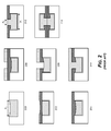
- FIG. 2 shows an example conventional approach for creating bonded features, when dishing is present.
- a substrate with a conductive feature with excessive dishing and dielectric erosion has a pad opening dimension P 1 .
- the substrate has been coated with one or more layers of dielectric material.
- the dielectric has been planarized.
- lithographic patterning is formed atop the planarized dielectric.
- single or dual damascene etching processes form a second pad opening P 2 , where P 2 is less than P 1 .
- a barrier layer and seed layer (not shown) have been placed, and metal deposition has occurred. The plated metal is annealed to partially stabilize the grains of the coated metal.
- metal planarization is performed.
- two damascene features are bonded after surface preparation and substrate assembly.
- the example conventional approach of FIG. 2 has some drawbacks and limitations. First, more than seven additional steps are needed to solve the initial dishing of the large damascene features after CMP. Secondly, the second pad opening P 2 in diagram 212 is always smaller than the first pad opening P 1 . Thirdly, this technique, used in some instances when creating direct bond interconnect (DBI®) hybrid bonding layers, can be relatively expensive. Fourth, the example conventional approach results in a loss of wiring freedom or design flexibility in which coplanar large metal and small metal features are components of the bonding surface.
- DBI® direct bond interconnect
- Advanced flat metals for microelectronics and advanced device packaging are provided. While conventional processes create large damascene features that have a large dishing defect, which causes failure in bonded devices, example systems and methods described herein create large damascene features that are planar. In one example, methods described herein create planar small, medium and large features on a bonding surface. In another example, the method of this invention creates a bonded apparatus wherein the bonded surfaces may comprise small, medium and large damascene cavities. In an implementation, large grains or large metallic crystals are formed in large (T c ) damascene cavities and much smaller grains or metallic crystals are formed in thinner (T f ) field metal regions.
- the etching rate or removal rate of the smaller metal grains in the field is higher than those of the large metal grains in the cavity.
- This differential removal rate between the field metal with thickness T f and cavity metal with larger thickness T c produces slightly domed metal features over damascene cavities. Further polishing of the substrate produces flat metal features over the various damascene cavities.
- the metal features are planar in metal widths varying from submicron features to features larger than 30 microns. In other embodiments, the width of the planar cavities exceeds 31 microns, and the related dishing may be less than 10 nm or, in many cases, less than 3 nm.
- layers of resist and layers of a second coating material may be applied in various ways to resist dishing during chemical-mechanical planarization (CMP), resulting in very flat damascene features.
- CMP chemical-mechanical planarization
- FIG. 1 is a diagram of a conventional dishing defect in the top surface of a metal feature.
- FIG. 2 is a diagram of a conventional approach for creating bonded damascene features, when dishing defects are conventionally present.
- FIG. 3 is a diagram showing an example process for forming a large planar metal feature for microelectronics.
- FIG. 4 is a diagram showing continuation steps of the example process of FIG. 3 .
- FIG. 5 is a diagram showing continuation steps of the example process of FIG. 3 .
- FIG. 6 is a diagram showing continuation steps of the example process of FIG. 3 .
- FIG. 7 is a diagram showing example variations of the process shown in FIGS. 3-6 .
- FIG. 8 is a diagram showing an example technique of masking the field of a substrate while plating a thick seed layer to fill damascene cavities with metal, as a variation when forming metal features with different grain sizes in the cavities versus the field, prior to performing CMP.
- FIG. 9 is a diagram showing an example technique of masking the field of a substrate while plating a thick seed layer to fill damascene cavities with metal to make the plated metal surface of the cavity layer higher than the surface of the field of the substrate, as a variation when forming metal features with different grain sizes in the cavities versus the field, prior to performing CMP.
- FIG. 10 is a diagram showing an example variation of the example process that includes selectively masking the metal fill over the damascene cavities to minimize dishing during planarization, as a variation when forming metal features with different grain sizes in the cavities versus the field, prior to performing CMP.
- FIG. 11 is a diagram showing an example variation of the example process that includes thinning a field metal thickness before annealing, as a variation when forming metal features with different grain sizes in the cavities versus the field, prior to performing CMP.
- FIG. 12 is a diagram showing an example variation of the example process of storing a substrate at a low temperature before thinning a field metal thickness, and then annealing at temperature to form different grain sizes in the open cavities versus the field of the substrate, prior to CMP.
- FIG. 13 is a diagram showing another example method of creating planar large damascene metal features, using selective coating on surfaces of the features to resist planarization forces that cause the dishing defect.
- FIG. 14 is a diagram showing an example variation of the example method of FIG. 13 of selectively coating the surface of the damascene features to resist planarization forces that cause dishing defects.
- FIG. 15 is a flow diagram of an example method of creating large flat conductive features.
- FIG. 16 is a flow diagram of an example continuation method of the example method shown in FIG. 15 .
- This disclosure describes advanced flat metals for microelectronics and packaging applications. While conventional processes create large damascene features that have high dishing defects that can cause failure in bonded devices, example systems and methods described herein create large damascene features that are planar or substantially planar.
- the metal after depositing metal within large cavities of a substrate, the metal is formed in such a manner that the metal is vertically thicker within the cavity than the metal on the surrounding field portion of the substrate nearby the cavities.
- An annealing process is applied, for example at approximately 25-150° C., which creates large metal grains and large metallic crystals of the metal, such as copper, within the larger cavities, and creates smaller metal grains and smaller metallic crystals of the copper on the thinner field portion of the substrate.
- the polishing rate and removal rate of the smaller metal grains in the field is higher than the polishing and removal rates of the large metal grains within the cavities.
- This differential removal rate between the field metal and the cavity metal produces slightly domed metal features over damascene cavities. Further polishing down to the substrate can produce flat metal features over the various large damascene cavities.
- the polished metal features have widths varying from the submicron range to metal features spanning cavities larger than 10 microns. In other embodiments, the width of the planar metal features spanning cavities exceeds 40 microns, and the related dishing is less than 10 nm, or sometimes even less than 3 nm, across the surface of the metal feature.
- the relatively large grains of copper within the damascene cavities have lower removal rates than the smaller copper grains in the field during chemical-mechanical planarization (CMP), resulting in very flat features across a die or across the surface of the planarized substrate.
- CMP chemical-mechanical planarization
- layers of resist and layers of a second coating material may be applied in various ways to further resist dishing defects during chemical-mechanical planarization (CMP), resulting in very flat damascene metal features.
- CMP chemical-mechanical planarization
- DBI® hybrid bonding is a low temperature direct bonding technology that allows wafer-to-wafer and die-to-wafer bonding with typically fine-pitch 3D electrical interconnects.
- the wafers or die surfaces are planarized and bond pads can be flat or slightly recessed in a dielectric layer.
- the wafers or die are then aligned and bonded at room temperature.
- the metal interconnects may be formed or improved during a subsequent higher temperature annealing step.
- the advanced flat metals described herein can also allow formation of the direct bond interface hybrid bonds at even lower temperatures than low temperatures used conventionally.
- FIG. 3 shows an example process for forming a large flat metal feature for microelectronics.
- the example process includes creating a pattern of cavities for metal features on a substrate of a microelectronic device, forming a metal layer on the patterned substrate, wherein the metal in the cavities is thicker than the metal coating at the field of the substrate, and then annealing the substrate and/or the metal at a temperature, for example, in the range of temperatures between 25-350° C. for a period of time varying between 30 seconds to 48 hours.
- the variables may depend on the plating bath additives and the concentration of impurities in the plated metal. The lower the impurity concentration in the plated metal, the lower the needed annealing temperature.
- Annealing at lower temperatures may be performed at a temperature in a range from room temperature to 100° C., for about 60 minutes, but in some circumstances from 4-48 hours. Similarly, the thicker the plated metal over the cavity, the lower the preferred annealing temperature.
- the annealing process generates metal grains of different sizes, with the sizes of the metal grains related to a thickness or a depth of the metal at each location on the substrate, including over the damascene cavities. In some examples, a higher temperature process may be utilized for a relatively shorter duration or, conversely, a lower temperature process may be utilized for a relatively longer length of time.
- the cavities formed have relatively large metal grains, while the metal coating on the field of the substrate has relatively small metal grains as compared to the grains in the cavity. In an implementation, a width of the grain size of a conductor within the conductive layer-filled cavity is more than 5% of the width of a cavity containing the metal feature.
- the metal is then planarized.
- the relatively larger metal grains in the cavity undergo removal more slowly than the relatively smaller metal grains of the field, forming a slightly raised or domed surface over the cavities. Further polishing results in a substantially flat metal feature.
- FIG. 3 further illustrates an implementation in which a barrier layer and a first seed layer are first deposited in a preformed cavity and on the field.
- the example process then includes depositing the metal on the first seed layer to partially fill the cavity and cover the field of the substrate with the metal, wherein the field layer of the metal has a depth of less than 0.6 microns and preferably less than 0.3 microns.
- Resist masking is selectively applied over the field portion of the substrate. Additional metal is deposited in the cavity to create a cavity layer of the metal thicker than the field layer of the metal. The resist masking is then cleaned or removed. It is of note that the thickness of the metal in the cavity T c is substantially larger than the thickness of the metal in the field T f .
- the depth of the cavity may vary between 1 to 7 microns or even higher and the ratio of metal thickness in the cavity (T c ) to that of the field metal (T f ) is at least 1.5 to 12 or even higher.
- the example process then includes thermally annealing the metal coated substrate at temperatures between 25-350° C. for times varying between 30 seconds up to 48 hours to form larger metal grains in the cavity and smaller metal grains in the field portion of the substrate.
- a chemical-mechanical planarization (CMP) process is performed on the substrate to remove material down to the barrier layer. Then, the barrier/adhesion layer covering the field is removed. While the process may be described with regard to one cavity, it should be appreciated that the technique can be expanded for multiple cavities of varying size across a given substrate.
- the cavity(ies) may have any of a number of shapes including round, square, polygonal, elongated, linear, or other suitable feature shape as needed for a given application.
- diagram 300 shows a barrier layer 302 and seed layer 304 coating placed in a large damascene cavity 306 in a substrate 308 .
- metal 312 is deposited over the substrate 308 to at least partially fill the large damascene cavity 306 .
- the thickness of metal deposited on the field of the substrate may be less than 0.6 microns, and preferably less than 0.3 microns, for example.
- a resist masking 316 is selectively applied on the top surface of the metal 312 on the field of the substrate.
- the thickness of the field metal 318 e.g., less than 0.6 ⁇
- additional metal 324 is plated or deposited in the unmasked large cavities, to form a thicker metal deposit 322 in the cavities, further assuring that the cavity metal 322 is thicker than the field metal 318 .
- the resist masking 316 is then cleaned off.
- an annealing process is applied, preferably at temperatures between 25-200° C. for times varying between 10 minutes to 2-12 hours, forming relatively smaller grains 330 of the metal in the thinner layer of the field metal 318 , and forming relatively larger grains 332 of the metal in the thicker cavity metal layer 322 .
- the plated substrate may be annealed with the resist layer 316 if the annealing temperature is kept below 150° C., for example.
- a CMP method is then used to remove the resist layer 316 and the unwanted metal overburden in the field T f .
- the large grains 332 of metal in the thicker cavity layer 322 resist an intermediate CMP process more than the smaller grains 330 of the metal in the thinner field layer 318 , leaving a dome or raised surface 336 over the cavities.
- the conductive metal is planarized, stopping at the barrier layer 302 .
- the barrier layer 302 is removed leaving a large planar damascene pad 342 or conductive feature, having a span of 10 ⁇ or more, for example.
- the surfaces of the substrate 402 with a large metal pad 404 or, in diagram 406 , a substrate 402 with multiple large pads 408 & 410 are processed for bonding.
- Diagrams 412 and 414 depict assembled and bonded substrates 402 & 402 ′, from the substrates that have one or more of the large conductive features in diagrams 400 and 406 .
- the DBI® hybrid bonding layer is freed from conventional limitations.
- the pad P 2 is conventionally limited to being smaller than the width of the pad P 1 beneath, as in diagram 212 . But the example methods and structures described herein enable elimination of such DBI® hybrid bonding layer limitations from the structure of the substrates, so that the top bonding pad 416 or via may be the same area as the pad 418 beneath.
- diagram 500 shows embodiments in which the polished metal features 502 & 504 & 506 bond with other instances of the polished metal features on substrates being bonded together.
- the polished metal features 502 & 504 & 506 as from the polish stage 340 shown in FIG. 3 , have widths varying from submicron scale to cavities larger than 30 microns.
- the width of one of the metal filled cavities of the bonded apparatus in FIG. 5 is more than 2 to 5 times the width of another metal filled cavity in the apparatus.
- the width of the planar cavities may exceed 40 microns, but the related dishing is less than 3 nm and less than 10 nm total across the surface of a die on the substrate or across the surface of the planarized substrate 402 .
- the planarized substrates 402 & 402 ′ with conductive features 504 ′ & 506 ′ & 508 ′ of varying widths made possible by the example methods described herein are further processed. This may include activating the surface of the dielectric layer, and also the metallic layer in some instances, then assembling face-to-face and contact-bonding together.
- both corresponding and non-corresponding large metal cavities with their metal features are aligned and bonded, such as large metal features 508 & 510 to smaller metal features 504 , and smaller metal features 514 & 516 & 518 & 520 to larger metal feature 512 .
- One or more traces, trenches, or vias may be bonded to larger conductive pads, enabled and facilitated by the highly planar surfaces of the metal features afforded by the example processes described herein.
- FIG. 6 shows one or more smaller dies 602 & 604 & 606 comprised of pads, trenches, vias of various sizes bonded to a larger substrate 608 comprised of pads, trenches and vias of various sizes.
- the width of the vias, trenches or pads on the bonding surfaces of substrate 608 and dies 602 , 604 and 606 may be between approximately 0.5-100 microns.
- the width of a conductive layer in a portion of the bonding surface of the substrate or the dies may be more than 30% the width of another conductive layer disposed on the bonding surfaces.
- the larger substrate 608 of two bonded dies or substrates may be larger than the smaller die 606 by more than 30% and die 606 may larger than die 604 by more than 50%, for example.
- the electrical conductive layer or pad on example die 602 may be smaller than the electrical conductive layer or pad on die 604 .
- multiple dies of various thicknesses may be directly bonded to the larger substrate 608 .
- die 602 may be more than 20% thicker than die 604 .
- substrate 608 may be thicker or thinner than one of the dies directly bonded to it.
- a first surface of a first substrate is bonded to a first surface of a second substrate.
- the first bonding surface of the first substrate is a conductive layer-filled cavity, the cavity having a width of at least 5 microns.
- a first bonding surface of the second substrate has one or more conductive layer-filled cavities, wherein a width of a grain size of a conductor within a conductive layer-filled cavity is more than 5% of the width of a cavity in the first or second substrate.
- Smaller bonded substrates may be microprocessors, memory devices, passive devices, optical devices, mechanical devices, MEMS devices, frequency filters, and/or a direct band gap device, and combinations of these and other devices.
- the back side of a first bonded die or substrate may be processed for subsequent bonding of one or more active devices, passive devices, optical devices, or MEMS devices, as described above.
- the pads are shown grossly exaggerated to highlight the contact structures; typically, the electrical conductive layers or structures are far smaller in relation to the associated die.
- FIG. 7 shows example variations of the process shown in FIGS. 3-6 .
- depositing the additional metal in the large cavities includes creating a cavity layer 702 of the metal and a field layer 704 of the metal that have coplanar top surfaces, and the cavity layer 702 of the metal is thicker than the field layer 704 of the metal.
- depositing the additional metal in the cavities includes creating a cavity layer 708 of the metal and a field layer 710 of the metal with non-coplanar top surfaces, wherein the surface of the cavity layer 708 is flat and is higher than the surface of the field layer 710 .
- depositing the additional metal in the cavities includes creating a cavity layer 714 of the metal and a field layer 716 of the metal with non-coplanar top surfaces, wherein the surface of the cavity layer 714 is non-flat, such as domed, and is mostly higher than the surface of the field layer 716 .
- FIG. 8 shows another example technique for making relatively large flat metal features, with little or no dipping.
- a substrate 800 is coated with a barrier layer 802 and a metallic seed layer 804 , in cavities 806 , such as damascene cavities, of the substrate 800 and on a field 808 of the substrate 800 .
- a mask 810 is applied to the field 808 of the substrate 800 .
- the substrate is plated with metal layer 812 to fill the seeded cavity 806 .
- the resist masking 810 is then removed 814 from the field layer 808 .
- additional metal 816 is deposited over the surface of the substrate 800 without the resist layer to form the new structure 816 with field thickness 820 and corresponding cavity metal 818 and the thickness of metal in the cavity T CU is substantially thicker than the thickness of the metal in the field T f .
- the process proceeds with thermally annealing 822 the substrate and layers, to make small grained metal 824 crystals over the field 808 , and large grained metal crystals 826 in the cavities 806 .
- An intermediate chemical-mechanical planarization (CMP) process 828 is applied on the cavity layer 818 of the metal and the field layer 820 of the metal.
- CMP chemical-mechanical planarization
- the cavity layer 818 of the metal is then planarized 830 down to the barrier layer 802 covering the field 808 .
- the barrier layer 802 is then removed from the field 808 , leaving the large metal damascene features 832 with a high degree of flatness, and with little or no dipping.
- FIG. 9 shows another alternative process for making large flat damascene features.
- a substrate 900 is coated with a barrier layer 902 and a metallic seed layer 904 , in cavities 906 , such as damascene cavities, of the substrate 900 and on a field 908 of the substrate 900 .
- a mask 910 is applied to the field 908 of the substrate 900 .
- a second seed layer may then be applied in the cavities 906 , the second seed layer having a thickness of at least 50 nm, for example.
- the first seed layer 904 or the second seed layer in the cavity 906 , as applicable, is then plated or deposited with metal 912 to fill the damascene cavities 906 , for forming metal features that have different grain sizes in the cavities 906 than on the fields 908 of the substrate 900 , prior to performing CMP.
- the deposited metal 912 has a thickness 914 that makes the top surface 916 of the deposited metal 912 higher than the top surface of the seed layer 904 under the resist masking material 910 .
- the resist masking 910 is then removed from the seed layer 904 of the metal on the field 908 of the substrate 900 .
- the cavity layer 914 of the metal is thicker than the field layer 918 of the metal.
- the substrate may be annealed with the resist layer 910 over the substrate prior to the removal of the resist layer 910 and the unwanted field metals by CMP methods.
- the process proceeds with thermally annealing the substrate and layers, to make small crystals 922 of grained metal over the field 908 , and large crystals 924 of grained metal in the cavities 906 .
- CMP chemical-mechanical planarization
- the cavity layer 914 of the metal is then planarized 932 down to the barrier layer 902 covering the field 908 .
- the barrier layer 902 is then removed from the field 908 , leaving the large metal damascene features 934 with a high degree of flatness, and with little or no dipping.
- FIG. 10 shows another alternative process for fabricating large flat damascene features.
- a substrate 1000 is coated with a barrier layer 1002 and a seed layer 1004 for depositing metal.
- a metal fill is deposited or plated on the seed layer 1004 , both in cavities 1006 of the substrate 1000 and on the surrounding fields 1008 of the substrate 1000 .
- a cavity layer 1010 of the metal has approximately the same thickness as a field layer 1012 of the metal, but with the field layer 1012 having a greater thickness than an overburden part 1014 over the cavity layer 1010 over the cavities 1006 .
- the top surface of the cavity layer 1010 is selectively covered with a masking material 1018 .
- the field layer 1012 of the metal is etched, so that a thickness of the cavity layer 1010 is now greater than a thickness of the field layer 1012 ′ of the metal.
- thermal annealing of the metal creates large grains 1024 of the metal in the cavity layer 1010 of the metal and relatively small grains 1026 of the metal in the field layer 1012 ′ of the metal.
- the cavity layer 1010 of the metal is planarized 1030 down to the barrier layer 1002 covering the field 1008 .
- the barrier layer 1002 is then removed from the field 1008 , leaving large flat metal damascene features with a high degree of flatness and little or no dipping.
- FIG. 11 shows another example process that includes thinning a field metal thickness before annealing, as a variation to the previous methods described above.
- the example process includes depositing a barrier layer 1102 and a first seed layer 1104 in the cavities 1106 and on the field 1108 of the substrate 1100 .
- a metal is deposited on the seed layer 1104 in the cavities 1106 and on the fields 1108 , creating a cavity layer 1110 of metal that is approximately the same thickness as the field layer 1112 of metal, with the field layer 1112 having a greater thickness than an overburden part 1114 of the cavity layer 1110 .
- the example process includes planarizing 1118 the cavity layer 1110 and the field layer 1112 to a substantially coplanar surface, so that the planarized field layer 1112 ′ has a thickness approximately equal to the overburden part 1114 of the cavity layer 1110 , and the field thickness is substantially thinner than the thickness of the metal in the cavity layer 1110 .
- the key requirement after the first metal removal or forming step is that the thickness of the metal within the cavity T c is substantially higher than the thickness of the metal in the field T f .
- the example process includes thermally annealing the metal to create large grains 1122 of the metal in the cavity layer 1110 of the metal and small grains 1124 of the metal in the field layer 1112 ′ of the metal.
- the cavity layer 1110 of the metal is planarized down 1128 to the barrier layer 1102 covering the field.
- the barrier layer 1102 is then removed from the field 1108 , leaving large area metal damascene features 1130 with a high degree of flatness, and little or no dipping of the top surfaces.
- the width of one or more of the large grains in the cavity 1106 is more than 3% of the width the cavity and is more than 10% in other embodiments.
- FIG. 12 shows a variation of the example process for making large flat metal features.
- a substrate is coated with a barrier layer 1202 and optionally a seed layer 1204 , and a metal 1206 is plated or deposited in the cavities 1208 and on the fields 1210 of the substrate 1200 .
- a cavity layer 1212 of the metal has a thickness approximately the same thickness as a field layer 1214 of the metal, and the field layer 1214 has a greater thickness than an overburden part 1216 of the cavity layer 1212 of the metal.
- the example process includes storing the plated substrate 1200 at a low temperature, for example at a temperature of 10° C. or lower, to preserve the submicron grain size of the plated metal 1206 .
- the lowered temperature also suppresses undesirable grain growth in the plated metal 1206 at room temperature, before thinning the plated metal 1206 .
- the top of the cooled field layer 1214 of metal and the cooled cavity layer 1212 of metal are planarized 1222 preferably at the low temperature for example below 20° C.
- the planarized field layer 1214 ′ has a thickness equal to or approximately equal to an overburden part 1216 over the cavity layer 1212 of metal over the cavities 1208 . It is preferable that the thickness of the metal in the field 1214 be less than 600 nm and less than 300 nm before the annealing step. Also, in some embodiments, the thickness of the metal over the barrier layer within the cavity may be may be more than 3 to 50 times the thickness of the planarized field metal 1228 .
- the metal 1206 now planarized is thermally annealed to create large grains 1226 of the metal in the cavity layer 1212 of the metal and small grains 1228 of the metal in the planarized field layer 1214 ′ of the metal.
- the cavity layer 1212 of the metal is planarized 1232 down to the barrier layer 1202 covering the field 1210 .
- the barrier layer 1202 is then removed from the fields 1210 , leaving the large metal features 1234 that have a high degree of flatness, with little or no dipping across their top surfaces.
- FIG. 13 shows another example method of creating planar large damascene metal features.
- the example method of FIG. 13 prevents dishing of the large metal features by selectively coating the surface of the features to resist planarization forces that cause the dishing defect.
- the example process of FIG. 13 may be used alone, or in conjunction with the formation of large metal grains that resist dishing, as in the methods described above.
- the example method begins with creating trenches or cavities 1302 for the metal features in the substrate 1300 .
- a barrier layer 1304 and a first seed layer 1306 are deposited in the cavities 1302 and on fields 1308 of the substrate.
- a metal 1312 is deposited, for example on a seed layer in the cavities 1302 , and on the fields 1308 to make a cavity layer 1314 of metal filling the cavities 1302 , the cavity layer 1314 approximately the same thickness as the field layers 1316 , and the field layer 1316 having a greater thickness than an overburden part 1318 of the cavity layer 1314 .
- a resist masking layer 1322 is applied over the field layers 1316 but not over the cavity layer 1314 .
- the example method continues with selectively applying a coating of a material 1326 over the cavity layer 1314 of metal.
- the coating 1326 may be an electrolytic material, a spin-on dielectric material, or an electrolessly coated layer, for example.
- the resist masking 1322 is cleaned from the field layer 1316 of metal.
- the cavity layer 1314 of the metal and the field layer 1316 of metal are planarized 1332 , leaving large flat metal damascene features 1334 .
- the planarization 1332 may be a chemical-mechanical planarization (CMP) process over the cavity layer 1314 and the field layer 1316 of the metal that achieves the flat conductive metal features 1334 .
- CMP chemical-mechanical planarization
- the coating 1326 on the cavity layer 1314 protects the cavity layer 1314 at least in part from the CMP process 1332 and prevents a dishing of the cavity layer 1314 while the CMP process 1332 removes the field layer 1316 .
- selectively applying a coating 1326 of material over the cavity layer 1314 includes selectively applying the coating 1326 over the cavity layer 1314 and on sidewalls 1336 of the field layer 1316 adjacent to the cavity layer 1314 but not over the resist masking layer 1322 over the field layer 1316 .
- FIG. 14 shows a variation of the example method of FIG. 13 , which describes selectively coating the surface of the damascene features to resist planarization forces that cause the dishing defect on large metal features.
- an etched substrate 1402 is plated with metal 1404 and planarized to obtain a substantially planar surface 1406 over both the cavities 1408 and fields 1410 of the substrate 1402 .
- resist masking 1412 is placed over the fields 1410 of the substrate.
- a coating 1414 of a material is also selectively applied over the unmasked cavity layer 1416 but not over the resist masking layer 1412 .
- the resist masking 1412 is removed, and the material coating 1414 is planarized 1420 to provide large damascene metal features 1422 that have a high degree of flatness, with little or no dipping across the top surface of the large metal features 1422 .
- the large planar metal features 1422 with little or no dipping across the top surfaces can be bonded together 1424 from different substrates, providing a substantial improvement over conventional limitations, such as that in diagram 212 ( FIG. 2 ), where dimension P 2 of a bonding surface made by conventional damascene methods applied to a die or substrate is necessarily less than dimension P 1 of the conventional die or substrate.
- the dimension of the bonding surface P 2 can be equal to ( 1424 ) or greater than ( 1426 ) dimension P 1 .
- This provides example structures, such as large metal bonding interface 1428 , that are not possible to produce, or not possible to easily produce conventionally without numerous extra steps that would make such a process conventionally unfeasible.
- the bonding surface of structure 212 conventionally comprises a second pad with a dimension P 2 smaller than the width of the first pad P 1 beneath.
- This conventional approach results in a loss of wiring freedom or design flexibility, limiting the use of coplanar large metal and small metal features and components in the bonding surface.
- the example methods described herein eliminate the restrictions of a smaller planar second pad overlaying a larger first pad, as imposed by the prior art.
- the example methods may be applied to form a bonding surface in which a width of the second pad P 2 is larger than the width of the first pad P 1 beneath.
- the width of one of the second pads may be 2-50 times larger than the width of the metal layer beneath.
- one or more of the cleaned planarized surfaces may be activated in a gentle nitrogen, boron, or fluoride plasma ambient or combinations thereof. The clean prepared surfaces are assembled with intimate contact and can be bonded by further thermal treatment of the coupled substrates.
- example apparatus has a first substrate beneath a second substrate, a bonding surface of the first substrate bonded to a bonding surface of the second substrate, and the bonding surface of the first substrate has conductive layer-filled cavities.
- a conductive layer-filled cavity of the bonding surface of the first substrate has a width of at least 5 microns, and the bonding surface of the second substrate also has conductive layer-filled cavities.
- a width of a conductive layer-filled cavity of the bonding surface of the second substrate is 2-20 times larger, for example, than a width of a conductive layer-filled cavity of the first substrate beneath the bonding surface of the second substrate.
- the barrier layer may serve as the seed layer. While in other applications, the seed layer and the plated material comprise similar materials.
- FIG. 15 shows an example method 1500 of creating large flat damascene conductive features.
- operations of the example method 1500 are shown in discreet blocks.
- a pattern of damascene cavities for metal features is etched or formed in or on a substrate for a microelectronic device.
- the substrate and the pattern are coated with a deposited metal, wherein the metal within the pattern of the damascene cavities has a greater thickness than the thickness of the metal on the field of the substrate.
- the metal is annealed to generate metal grains of different sizes, the sizes of the metal grains related to a thickness or a depth of the metal at each location over the un-etched substrate and over the etched pattern of damascene cavities, the metal in the pattern of damascene cavities annealing to relatively large metal grains and the metal that is coating the fields of the substrate annealing to relatively small metal grains.
- the metal is planarized, wherein the large metal grains in the pattern of damascene cavities planarize to flat metal features with a minimum dishing defect from the planarization.
- the example method 1500 may end at block 1508 , with the flat metal features planarized with a minimum dishing defect. Variations of this example method, and other processes useful for forming the large flat metal features, are also shown in FIGS. 2-14 .
- FIG. 16 shows optional continuation steps 1600 of the example method 1500 , for further processing.
- the surface of the planar substrates with flat metal features are processed for bonding.
- the processed surface of the substrate is aligned and bonded face-to-face with another instance of a processed surface of another substrate that has flat metal features, at room temperature or at low temperatures.
- the bonded substrates are thermally exposed to a higher temperature in order for the opposing conductive layers of the opposing flat metal features to fuse together permanently.
- a backside of the first bonded substrate is processed for bonding with another additional substrate.
Abstract
Description
Claims (14)
Priority Applications (4)
| Application Number | Priority Date | Filing Date | Title |
|---|---|---|---|
| US15/994,435 US10446441B2 (en) | 2017-06-05 | 2018-05-31 | Flat metal features for microelectronics applications |
| PCT/US2018/035947 WO2018226618A1 (en) | 2017-06-05 | 2018-06-05 | Flat metal features for microelectronics applications |
| US16/563,512 US10840135B2 (en) | 2017-06-05 | 2019-09-06 | Flat metal features for microelectronics applications |
| US17/098,128 US11908739B2 (en) | 2017-06-05 | 2020-11-13 | Flat metal features for microelectronics applications |
Applications Claiming Priority (2)
| Application Number | Priority Date | Filing Date | Title |
|---|---|---|---|
| US201762515410P | 2017-06-05 | 2017-06-05 | |
| US15/994,435 US10446441B2 (en) | 2017-06-05 | 2018-05-31 | Flat metal features for microelectronics applications |
Related Child Applications (1)
| Application Number | Title | Priority Date | Filing Date |
|---|---|---|---|
| US16/563,512 Division US10840135B2 (en) | 2017-06-05 | 2019-09-06 | Flat metal features for microelectronics applications |
Publications (2)
| Publication Number | Publication Date |
|---|---|
| US20180350674A1 US20180350674A1 (en) | 2018-12-06 |
| US10446441B2 true US10446441B2 (en) | 2019-10-15 |
Family
ID=64458372
Family Applications (3)
| Application Number | Title | Priority Date | Filing Date |
|---|---|---|---|
| US15/994,435 Active US10446441B2 (en) | 2017-06-05 | 2018-05-31 | Flat metal features for microelectronics applications |
| US16/563,512 Active US10840135B2 (en) | 2017-06-05 | 2019-09-06 | Flat metal features for microelectronics applications |
| US17/098,128 Active 2039-06-20 US11908739B2 (en) | 2017-06-05 | 2020-11-13 | Flat metal features for microelectronics applications |
Family Applications After (2)
| Application Number | Title | Priority Date | Filing Date |
|---|---|---|---|
| US16/563,512 Active US10840135B2 (en) | 2017-06-05 | 2019-09-06 | Flat metal features for microelectronics applications |
| US17/098,128 Active 2039-06-20 US11908739B2 (en) | 2017-06-05 | 2020-11-13 | Flat metal features for microelectronics applications |
Country Status (2)
| Country | Link |
|---|---|
| US (3) | US10446441B2 (en) |
| WO (1) | WO2018226618A1 (en) |
Families Citing this family (51)
| Publication number | Priority date | Publication date | Assignee | Title |
|---|---|---|---|---|
| US7109092B2 (en) | 2003-05-19 | 2006-09-19 | Ziptronix, Inc. | Method of room temperature covalent bonding |
| US8735219B2 (en) | 2012-08-30 | 2014-05-27 | Ziptronix, Inc. | Heterogeneous annealing method and device |
| US10886250B2 (en) | 2015-07-10 | 2021-01-05 | Invensas Corporation | Structures and methods for low temperature bonding using nanoparticles |
| US10204893B2 (en) | 2016-05-19 | 2019-02-12 | Invensas Bonding Technologies, Inc. | Stacked dies and methods for forming bonded structures |
| US10719762B2 (en) | 2017-08-03 | 2020-07-21 | Xcelsis Corporation | Three dimensional chip structure implementing machine trained network |
| US10580735B2 (en) | 2016-10-07 | 2020-03-03 | Xcelsis Corporation | Stacked IC structure with system level wiring on multiple sides of the IC die |
| US10002844B1 (en) | 2016-12-21 | 2018-06-19 | Invensas Bonding Technologies, Inc. | Bonded structures |
| KR20230156179A (en) | 2016-12-29 | 2023-11-13 | 아데이아 세미컨덕터 본딩 테크놀로지스 인코포레이티드 | Bonded structures with integrated passive component |
| US10629577B2 (en) | 2017-03-16 | 2020-04-21 | Invensas Corporation | Direct-bonded LED arrays and applications |
| US10515913B2 (en) | 2017-03-17 | 2019-12-24 | Invensas Bonding Technologies, Inc. | Multi-metal contact structure |
| US10269756B2 (en) | 2017-04-21 | 2019-04-23 | Invensas Bonding Technologies, Inc. | Die processing |
| US10879212B2 (en) | 2017-05-11 | 2020-12-29 | Invensas Bonding Technologies, Inc. | Processed stacked dies |
| US10446441B2 (en) | 2017-06-05 | 2019-10-15 | Invensas Corporation | Flat metal features for microelectronics applications |
| US10840205B2 (en) * | 2017-09-24 | 2020-11-17 | Invensas Bonding Technologies, Inc. | Chemical mechanical polishing for hybrid bonding |
| US11031285B2 (en) | 2017-10-06 | 2021-06-08 | Invensas Bonding Technologies, Inc. | Diffusion barrier collar for interconnects |
| US11380597B2 (en) | 2017-12-22 | 2022-07-05 | Invensas Bonding Technologies, Inc. | Bonded structures |
| US10727219B2 (en) | 2018-02-15 | 2020-07-28 | Invensas Bonding Technologies, Inc. | Techniques for processing devices |
| US11169326B2 (en) | 2018-02-26 | 2021-11-09 | Invensas Bonding Technologies, Inc. | Integrated optical waveguides, direct-bonded waveguide interface joints, optical routing and interconnects |
| US11056348B2 (en) | 2018-04-05 | 2021-07-06 | Invensas Bonding Technologies, Inc. | Bonding surfaces for microelectronics |
| US10790262B2 (en) | 2018-04-11 | 2020-09-29 | Invensas Bonding Technologies, Inc. | Low temperature bonded structures |
| US10964664B2 (en) | 2018-04-20 | 2021-03-30 | Invensas Bonding Technologies, Inc. | DBI to Si bonding for simplified handle wafer |
| US11004757B2 (en) | 2018-05-14 | 2021-05-11 | Invensas Bonding Technologies, Inc. | Bonded structures |
| US11276676B2 (en) | 2018-05-15 | 2022-03-15 | Invensas Bonding Technologies, Inc. | Stacked devices and methods of fabrication |
| CN112585740A (en) | 2018-06-13 | 2021-03-30 | 伊文萨思粘合技术公司 | TSV as a pad |
| US11393779B2 (en) | 2018-06-13 | 2022-07-19 | Invensas Bonding Technologies, Inc. | Large metal pads over TSV |
| US10910344B2 (en) | 2018-06-22 | 2021-02-02 | Xcelsis Corporation | Systems and methods for releveled bump planes for chiplets |
| US11664357B2 (en) | 2018-07-03 | 2023-05-30 | Adeia Semiconductor Bonding Technologies Inc. | Techniques for joining dissimilar materials in microelectronics |
| US11158606B2 (en) | 2018-07-06 | 2021-10-26 | Invensas Bonding Technologies, Inc. | Molded direct bonded and interconnected stack |
| US11515291B2 (en) | 2018-08-28 | 2022-11-29 | Adeia Semiconductor Inc. | Integrated voltage regulator and passive components |
| US11158573B2 (en) | 2018-10-22 | 2021-10-26 | Invensas Bonding Technologies, Inc. | Interconnect structures |
| WO2020150159A1 (en) | 2019-01-14 | 2020-07-23 | Invensas Bonding Technologies, Inc. | Bonded structures |
| US11901281B2 (en) | 2019-03-11 | 2024-02-13 | Adeia Semiconductor Bonding Technologies Inc. | Bonded structures with integrated passive component |
| US10854578B2 (en) | 2019-03-29 | 2020-12-01 | Invensas Corporation | Diffused bitline replacement in stacked wafer memory |
| US11373963B2 (en) | 2019-04-12 | 2022-06-28 | Invensas Bonding Technologies, Inc. | Protective elements for bonded structures |
| CN110085515B (en) * | 2019-04-30 | 2021-04-13 | 德淮半导体有限公司 | Wafer bonding method |
| US11296053B2 (en) | 2019-06-26 | 2022-04-05 | Invensas Bonding Technologies, Inc. | Direct bonded stack structures for increased reliability and improved yield in microelectronics |
| CN112309836B (en) * | 2019-08-01 | 2022-10-28 | 京东方科技集团股份有限公司 | Back plate, preparation method thereof, backlight module and display device |
| US11862602B2 (en) | 2019-11-07 | 2024-01-02 | Adeia Semiconductor Technologies Llc | Scalable architecture for reduced cycles across SOC |
| US11762200B2 (en) | 2019-12-17 | 2023-09-19 | Adeia Semiconductor Bonding Technologies Inc. | Bonded optical devices |
| US11876076B2 (en) | 2019-12-20 | 2024-01-16 | Adeia Semiconductor Technologies Llc | Apparatus for non-volatile random access memory stacks |
| US11721653B2 (en) | 2019-12-23 | 2023-08-08 | Adeia Semiconductor Bonding Technologies Inc. | Circuitry for electrical redundancy in bonded structures |
| KR20220120631A (en) | 2019-12-23 | 2022-08-30 | 인벤사스 본딩 테크놀로지스 인코포레이티드 | Electrical Redundancy for Bonded Structures |
| US11742314B2 (en) | 2020-03-31 | 2023-08-29 | Adeia Semiconductor Bonding Technologies Inc. | Reliable hybrid bonded apparatus |
| US11735523B2 (en) | 2020-05-19 | 2023-08-22 | Adeia Semiconductor Bonding Technologies Inc. | Laterally unconfined structure |
| US11631647B2 (en) | 2020-06-30 | 2023-04-18 | Adeia Semiconductor Bonding Technologies Inc. | Integrated device packages with integrated device die and dummy element |
| EP3945566A1 (en) | 2020-07-29 | 2022-02-02 | Imec VZW | A method for wafer to wafer hybrid bonding, enabling improved metal-to-metal contact and higher density of interconnect pads |
| US11764177B2 (en) | 2020-09-04 | 2023-09-19 | Adeia Semiconductor Bonding Technologies Inc. | Bonded structure with interconnect structure |
| US11728273B2 (en) | 2020-09-04 | 2023-08-15 | Adeia Semiconductor Bonding Technologies Inc. | Bonded structure with interconnect structure |
| US11264357B1 (en) | 2020-10-20 | 2022-03-01 | Invensas Corporation | Mixed exposure for large die |
| US20220208702A1 (en) * | 2020-12-30 | 2022-06-30 | Invensas Bonding Technologies, Inc. | Structure with conductive feature and method of forming same |
| CN117256047A (en) * | 2021-03-03 | 2023-12-19 | 美商艾德亚半导体接合科技有限公司 | Contact structure for direct bonding |
Citations (7)
| Publication number | Priority date | Publication date | Assignee | Title |
|---|---|---|---|---|
| JP2000183061A (en) | 1998-12-18 | 2000-06-30 | Rohm Co Ltd | Manufacture of semiconductor device |
| US6117784A (en) | 1997-11-12 | 2000-09-12 | International Business Machines Corporation | Process for integrated circuit wiring |
| US20040052930A1 (en) | 2000-04-27 | 2004-03-18 | Bulent Basol | Conductive structure fabrication process using novel layered structure and conductive structure fabricated thereby for use in multi-level metallization |
| US20040238492A1 (en) | 2003-04-23 | 2004-12-02 | Catabay Wilbur G. | Planarization with reduced dishing |
| KR20080050129A (en) | 2006-12-01 | 2008-06-05 | 삼성전자주식회사 | Photo diode and image sensor employing the same |
| US20130009321A1 (en) | 2011-07-05 | 2013-01-10 | Sony Corporation | Semiconductor device, fabrication method for a semiconductor device and electronic apparatus |
| US8728934B2 (en) | 2011-06-24 | 2014-05-20 | Tessera, Inc. | Systems and methods for producing flat surfaces in interconnect structures |
Family Cites Families (313)
| Publication number | Priority date | Publication date | Assignee | Title |
|---|---|---|---|---|
| KR900008647B1 (en) | 1986-03-20 | 1990-11-26 | 후지쓰 가부시끼가이샤 | A method for manufacturing three demensional i.c. |
| JPH0272642A (en) | 1988-09-07 | 1990-03-12 | Nec Corp | Structure and method for connecting substrates |
| JPH0344067A (en) | 1989-07-11 | 1991-02-25 | Nec Corp | Laminating method of semiconductor substrate |
| US5489804A (en) | 1989-08-28 | 1996-02-06 | Lsi Logic Corporation | Flexible preformed planar structures for interposing between a chip and a substrate |
| CA2083072C (en) | 1991-11-21 | 1998-02-03 | Shinichi Hasegawa | Method for manufacturing polyimide multilayer wiring substrate |
| US6008126A (en) | 1992-04-08 | 1999-12-28 | Elm Technology Corporation | Membrane dielectric isolation IC fabrication |
| US5236118A (en) | 1992-05-12 | 1993-08-17 | The Regents Of The University Of California | Aligned wafer bonding |
| US5503704A (en) | 1993-01-06 | 1996-04-02 | The Regents Of The University Of California | Nitrogen based low temperature direct bonding |
| US5516727A (en) | 1993-04-19 | 1996-05-14 | International Business Machines Corporation | Method for encapsulating light emitting diodes |
| JPH07193294A (en) | 1993-11-01 | 1995-07-28 | Matsushita Electric Ind Co Ltd | Electronic component and its manufacture |
| US5501003A (en) | 1993-12-15 | 1996-03-26 | Bel Fuse Inc. | Method of assembling electronic packages for surface mount applications |
| US5442235A (en) | 1993-12-23 | 1995-08-15 | Motorola Inc. | Semiconductor device having an improved metal interconnect structure |
| US5413952A (en) | 1994-02-02 | 1995-05-09 | Motorola, Inc. | Direct wafer bonded structure method of making |
| CN1112286A (en) | 1994-05-19 | 1995-11-22 | 陆敬良 | Durable neon lamp and its making technique |
| KR960009074A (en) | 1994-08-29 | 1996-03-22 | 모리시다 요이치 | Semiconductor device and manufacturing method thereof |
| DE4433330C2 (en) | 1994-09-19 | 1997-01-30 | Fraunhofer Ges Forschung | Method for producing semiconductor structures with advantageous high-frequency properties and a semiconductor wafer structure |
| JP2679681B2 (en) | 1995-04-28 | 1997-11-19 | 日本電気株式会社 | Semiconductor device, package for semiconductor device, and manufacturing method thereof |
| US5610431A (en) | 1995-05-12 | 1997-03-11 | The Charles Stark Draper Laboratory, Inc. | Covers for micromechanical sensors and other semiconductor devices |
| JP3979687B2 (en) | 1995-10-26 | 2007-09-19 | アプライド マテリアルズ インコーポレイテッド | Method for improving film stability of halogen-doped silicon oxide films |
| KR100438256B1 (en) | 1995-12-18 | 2004-08-25 | 마츠시타 덴끼 산교 가부시키가이샤 | Semiconductor device and manufacturing method |
| ATE204251T1 (en) | 1996-05-14 | 2001-09-15 | Degussa | METHOD FOR PRODUCING TRIMETHYLHYDROQUINONE |
| US5956605A (en) | 1996-09-20 | 1999-09-21 | Micron Technology, Inc. | Use of nitrides for flip-chip encapsulation |
| US5821692A (en) | 1996-11-26 | 1998-10-13 | Motorola, Inc. | Organic electroluminescent device hermetic encapsulation package |
| EP0951064A4 (en) | 1996-12-24 | 2005-02-23 | Nitto Denko Corp | Manufacture of semiconductor device |
| US6221753B1 (en) | 1997-01-24 | 2001-04-24 | Micron Technology, Inc. | Flip chip technique for chip assembly |
| US5929512A (en) | 1997-03-18 | 1999-07-27 | Jacobs; Richard L. | Urethane encapsulated integrated circuits and compositions therefor |
| JP4032454B2 (en) | 1997-06-27 | 2008-01-16 | ソニー株式会社 | Manufacturing method of three-dimensional circuit element |
| US6097096A (en) | 1997-07-11 | 2000-08-01 | Advanced Micro Devices | Metal attachment method and structure for attaching substrates at low temperatures |
| US6137063A (en) | 1998-02-27 | 2000-10-24 | Micron Technology, Inc. | Electrical interconnections |
| EP0951068A1 (en) | 1998-04-17 | 1999-10-20 | Interuniversitair Micro-Elektronica Centrum Vzw | Method of fabrication of a microstructure having an inside cavity |
| US6147000A (en) | 1998-08-11 | 2000-11-14 | Advanced Micro Devices, Inc. | Method for forming low dielectric passivation of copper interconnects |
| US6316786B1 (en) | 1998-08-29 | 2001-11-13 | International Business Machines Corporation | Organic opto-electronic devices |
| SG99289A1 (en) | 1998-10-23 | 2003-10-27 | Ibm | Chemical-mechanical planarization of metallurgy |
| US6409904B1 (en) | 1998-12-01 | 2002-06-25 | Nutool, Inc. | Method and apparatus for depositing and controlling the texture of a thin film |
| US6123825A (en) | 1998-12-02 | 2000-09-26 | International Business Machines Corporation | Electromigration-resistant copper microstructure and process of making |
| US6232150B1 (en) | 1998-12-03 | 2001-05-15 | The Regents Of The University Of Michigan | Process for making microstructures and microstructures made thereby |
| US6348709B1 (en) | 1999-03-15 | 2002-02-19 | Micron Technology, Inc. | Electrical contact for high dielectric constant capacitors and method for fabricating the same |
| JP3532788B2 (en) | 1999-04-13 | 2004-05-31 | 唯知 須賀 | Semiconductor device and manufacturing method thereof |
| US6259160B1 (en) | 1999-04-21 | 2001-07-10 | Advanced Micro Devices, Inc. | Apparatus and method of encapsulated copper (Cu) Interconnect formation |
| US6258625B1 (en) | 1999-05-18 | 2001-07-10 | International Business Machines Corporation | Method of interconnecting electronic components using a plurality of conductive studs |
| KR100333384B1 (en) | 1999-06-28 | 2002-04-18 | 박종섭 | chip size stack package and method of fabricating the same |
| US6465376B2 (en) * | 1999-08-18 | 2002-10-15 | International Business Machines Corporation | Method and structure for improving electromigration of chip interconnects |
| US6756253B1 (en) | 1999-08-27 | 2004-06-29 | Micron Technology, Inc. | Method for fabricating a semiconductor component with external contact polymer support layer |
| US6583515B1 (en) | 1999-09-03 | 2003-06-24 | Texas Instruments Incorporated | Ball grid array package for enhanced stress tolerance |
| US6984571B1 (en) | 1999-10-01 | 2006-01-10 | Ziptronix, Inc. | Three dimensional device integration method and integrated device |
| US6500694B1 (en) | 2000-03-22 | 2002-12-31 | Ziptronix, Inc. | Three dimensional device integration method and integrated device |
| US6333120B1 (en) | 1999-10-27 | 2001-12-25 | International Business Machines Corporation | Method for controlling the texture and microstructure of plated copper and plated structure |
| US6902987B1 (en) | 2000-02-16 | 2005-06-07 | Ziptronix, Inc. | Method for low temperature bonding and bonded structure |
| US6326698B1 (en) | 2000-06-08 | 2001-12-04 | Micron Technology, Inc. | Semiconductor devices having protective layers thereon through which contact pads are exposed and stereolithographic methods of fabricating such semiconductor devices |
| JP4322402B2 (en) | 2000-06-22 | 2009-09-02 | 大日本印刷株式会社 | Printed wiring board and manufacturing method thereof |
| JP3440057B2 (en) | 2000-07-05 | 2003-08-25 | 唯知 須賀 | Semiconductor device and manufacturing method thereof |
| US6423640B1 (en) | 2000-08-09 | 2002-07-23 | Taiwan Semiconductor Manufacturing Co., Ltd. | Headless CMP process for oxide planarization |
| US6583460B1 (en) | 2000-08-29 | 2003-06-24 | Micron Technology, Inc. | Method of forming a metal to polysilicon contact in oxygen environment |
| US6600224B1 (en) | 2000-10-31 | 2003-07-29 | International Business Machines Corporation | Thin film attachment to laminate using a dendritic interconnection |
| US6552436B2 (en) | 2000-12-08 | 2003-04-22 | Motorola, Inc. | Semiconductor device having a ball grid array and method therefor |
| JP2002353416A (en) | 2001-05-25 | 2002-12-06 | Sony Corp | Semiconductor storage device and manufacturing method therefor |
| US6555917B1 (en) | 2001-10-09 | 2003-04-29 | Amkor Technology, Inc. | Semiconductor package having stacked semiconductor chips and method of making the same |
| US6667225B2 (en) | 2001-12-17 | 2003-12-23 | Intel Corporation | Wafer-bonding using solder and method of making the same |
| US6660564B2 (en) | 2002-01-25 | 2003-12-09 | Sony Corporation | Wafer-level through-wafer packaging process for MEMS and MEMS package produced thereby |
| US6624003B1 (en) | 2002-02-06 | 2003-09-23 | Teravicta Technologies, Inc. | Integrated MEMS device and package |
| US6887769B2 (en) | 2002-02-06 | 2005-05-03 | Intel Corporation | Dielectric recess for wafer-to-wafer and die-to-die metal bonding and method of fabricating the same |
| US6762076B2 (en) | 2002-02-20 | 2004-07-13 | Intel Corporation | Process of vertically stacking multiple wafers supporting different active integrated circuit (IC) devices |
| US6627814B1 (en) | 2002-03-22 | 2003-09-30 | David H. Stark | Hermetically sealed micro-device package with window |
| US7105980B2 (en) | 2002-07-03 | 2006-09-12 | Sawtek, Inc. | Saw filter device and method employing normal temperature bonding for producing desirable filter production and performance characteristics |
| JP4083502B2 (en) | 2002-08-19 | 2008-04-30 | 株式会社フジミインコーポレーテッド | Polishing method and polishing composition used therefor |
| US20040052390A1 (en) * | 2002-09-12 | 2004-03-18 | Nelson Morales | Method and apparatus for programming a hearing device |
| US7023093B2 (en) | 2002-10-24 | 2006-04-04 | International Business Machines Corporation | Very low effective dielectric constant interconnect Structures and methods for fabricating the same |
| US20040108136A1 (en) | 2002-12-04 | 2004-06-10 | International Business Machines Corporation | Structure comprising a barrier layer of a tungsten alloy comprising cobalt and/or nickel |
| US7354798B2 (en) | 2002-12-20 | 2008-04-08 | International Business Machines Corporation | Three-dimensional device fabrication method |
| US6962835B2 (en) | 2003-02-07 | 2005-11-08 | Ziptronix, Inc. | Method for room temperature metal direct bonding |
| US7135780B2 (en) | 2003-02-12 | 2006-11-14 | Micron Technology, Inc. | Semiconductor substrate for build-up packages |
| US6908027B2 (en) | 2003-03-31 | 2005-06-21 | Intel Corporation | Complete device layer transfer without edge exclusion via direct wafer bonding and constrained bond-strengthening process |
| US7109092B2 (en) | 2003-05-19 | 2006-09-19 | Ziptronix, Inc. | Method of room temperature covalent bonding |
| TWI275168B (en) | 2003-06-06 | 2007-03-01 | Sanyo Electric Co | Semiconductor device and method for making the same |
| US6867073B1 (en) | 2003-10-21 | 2005-03-15 | Ziptronix, Inc. | Single mask via method and device |
| KR100618855B1 (en) | 2004-08-02 | 2006-09-01 | 삼성전자주식회사 | Method of forming metal contact structure and method of fabricating phase-change memory using the same |
| US20060057945A1 (en) | 2004-09-16 | 2006-03-16 | Chia-Lin Hsu | Chemical mechanical polishing process |
| JP4542926B2 (en) | 2005-03-15 | 2010-09-15 | 株式会社東芝 | Joining method |
| US7998335B2 (en) | 2005-06-13 | 2011-08-16 | Cabot Microelectronics Corporation | Controlled electrochemical polishing method |
| US7485968B2 (en) | 2005-08-11 | 2009-02-03 | Ziptronix, Inc. | 3D IC method and device |
| US7193423B1 (en) | 2005-12-12 | 2007-03-20 | International Business Machines Corporation | Wafer-to-wafer alignments |
| US8101858B2 (en) | 2006-03-14 | 2012-01-24 | Corus Technology B.V. | Chalcopyrite semiconductor based photovoltaic solar cell comprising a metal substrate, coated metal substrate for a photovoltaic solar cell and manufacturing method thereof |
| US7750488B2 (en) | 2006-07-10 | 2010-07-06 | Tezzaron Semiconductor, Inc. | Method for bonding wafers to produce stacked integrated circuits |
| US8241995B2 (en) | 2006-09-18 | 2012-08-14 | International Business Machines Corporation | Bonding of substrates including metal-dielectric patterns with metal raised above dielectric |
| US20080073795A1 (en) | 2006-09-24 | 2008-03-27 | Georgia Tech Research Corporation | Integrated circuit interconnection devices and methods |
| KR100825648B1 (en) | 2006-11-29 | 2008-04-25 | 동부일렉트로닉스 주식회사 | Semiconductor device and method of manufacturing the same |
| US9343330B2 (en) | 2006-12-06 | 2016-05-17 | Cabot Microelectronics Corporation | Compositions for polishing aluminum/copper and titanium in damascene structures |
| US7803693B2 (en) | 2007-02-15 | 2010-09-28 | John Trezza | Bowed wafer hybridization compensation |
| WO2009021266A1 (en) | 2007-08-15 | 2009-02-19 | Christophe Alain Guex | Vessel transporting apparatus and method |
| US8168532B2 (en) | 2007-11-14 | 2012-05-01 | Fujitsu Limited | Method of manufacturing a multilayer interconnection structure in a semiconductor device |
| US8435421B2 (en) | 2007-11-27 | 2013-05-07 | Cabot Microelectronics Corporation | Metal-passivating CMP compositions and methods |
| DE102008007001B4 (en) | 2008-01-31 | 2016-09-22 | Globalfoundries Dresden Module One Limited Liability Company & Co. Kg | Increasing the resistance to electromigration in a connection structure of a semiconductor device by forming an alloy |
| US20090200668A1 (en) | 2008-02-07 | 2009-08-13 | International Business Machines Corporation | Interconnect structure with high leakage resistance |
| US20100327443A1 (en) | 2008-02-22 | 2010-12-30 | Barun Electronics, Co., Ltd. | Joining structure and a substrate-joining method using the same |
| US8349635B1 (en) | 2008-05-20 | 2013-01-08 | Silicon Laboratories Inc. | Encapsulated MEMS device and method to form the same |
| US9893004B2 (en) | 2011-07-27 | 2018-02-13 | Broadpak Corporation | Semiconductor interposer integration |
| KR100945800B1 (en) | 2008-12-09 | 2010-03-05 | 김영혜 | Method for manufacturing heterogeneous bonded wafer |
| US8476165B2 (en) | 2009-04-01 | 2013-07-02 | Tokyo Electron Limited | Method for thinning a bonding wafer |
| US8242600B2 (en) | 2009-05-19 | 2012-08-14 | International Business Machines Corporation | Redundant metal barrier structure for interconnect applications |
| US8039966B2 (en) | 2009-09-03 | 2011-10-18 | International Business Machines Corporation | Structures of and methods and tools for forming in-situ metallic/dielectric caps for interconnects |
| US8101517B2 (en) | 2009-09-29 | 2012-01-24 | Infineon Technologies Ag | Semiconductor device and method for making same |
| US8482132B2 (en) | 2009-10-08 | 2013-07-09 | International Business Machines Corporation | Pad bonding employing a self-aligned plated liner for adhesion enhancement |
| FR2954585B1 (en) | 2009-12-23 | 2012-03-02 | Soitec Silicon Insulator Technologies | METHOD FOR MAKING A HETEROSTRUCTURE WITH MINIMIZATION OF STRESS |
| JP5517800B2 (en) | 2010-07-09 | 2014-06-11 | キヤノン株式会社 | Member for solid-state imaging device and method for manufacturing solid-state imaging device |
| FR2966283B1 (en) | 2010-10-14 | 2012-11-30 | Soi Tec Silicon On Insulator Tech Sa | METHOD FOR PRODUCING A COLLAGE STRUCTURE |
| US8377798B2 (en) | 2010-11-10 | 2013-02-19 | Taiwan Semiconductor Manufacturing Co., Ltd | Method and structure for wafer to wafer bonding in semiconductor packaging |
| US8476146B2 (en) | 2010-12-03 | 2013-07-02 | Taiwan Semiconductor Manufacturing Company, Ltd. | Reducing wafer distortion through a low CTE layer |
| US8620164B2 (en) | 2011-01-20 | 2013-12-31 | Intel Corporation | Hybrid III-V silicon laser formed by direct bonding |
| US8988299B2 (en) | 2011-02-17 | 2015-03-24 | International Business Machines Corporation | Integrated antenna for RFIC package applications |
| JP2012174988A (en) | 2011-02-23 | 2012-09-10 | Sony Corp | Junction electrode, manufacturing method of the junction electrode, semiconductor device, and manufacturing method of the semiconductor device |
| US8501537B2 (en) | 2011-03-31 | 2013-08-06 | Soitec | Methods for bonding semiconductor structures involving annealing processes, and bonded semiconductor structures formed using such methods |
| US8716105B2 (en) | 2011-03-31 | 2014-05-06 | Soitec | Methods for bonding semiconductor structures involving annealing processes, and bonded semiconductor structures and intermediate structures formed using such methods |
| KR102084337B1 (en) | 2011-05-24 | 2020-04-23 | 소니 주식회사 | Semiconductor device |
| JP5982748B2 (en) | 2011-08-01 | 2016-08-31 | ソニー株式会社 | SEMICONDUCTOR DEVICE, SEMICONDUCTOR DEVICE MANUFACTURING METHOD, AND ELECTRONIC DEVICE |
| US8697493B2 (en) | 2011-07-18 | 2014-04-15 | Soitec | Bonding surfaces for direct bonding of semiconductor structures |
| US8441131B2 (en) | 2011-09-12 | 2013-05-14 | Globalfoundries Inc. | Strain-compensating fill patterns for controlling semiconductor chip package interactions |
| US8785790B2 (en) | 2011-11-10 | 2014-07-22 | Invensas Corporation | High strength through-substrate vias |
| US8916781B2 (en) | 2011-11-15 | 2014-12-23 | Invensas Corporation | Cavities containing multi-wiring structures and devices |
| US9269612B2 (en) | 2011-11-22 | 2016-02-23 | Taiwan Semiconductor Manufacturing Company, Ltd. | Mechanisms of forming damascene interconnect structures |
| US8796851B2 (en) | 2012-01-05 | 2014-08-05 | Taiwan Semiconductor Manufacturing Company, Ltd. | Bonding pad and method of making same |
| US8796853B2 (en) | 2012-02-24 | 2014-08-05 | International Business Machines Corporation | Metallic capped interconnect structure with high electromigration resistance and low resistivity |
| FR2987626B1 (en) | 2012-03-05 | 2015-04-03 | Commissariat Energie Atomique | DIRECT COLLECTION METHOD USING COMPRESSIBLE POROUS LAYER |
| CN103377911B (en) | 2012-04-16 | 2016-09-21 | 中国科学院微电子研究所 | The method improving CMP process uniformity |
| US10453996B2 (en) | 2012-05-04 | 2019-10-22 | Stc.Unm | Growth of cubic crystalline phase structure on silicon substrates and devices comprising the cubic crystalline phase structure |
| US8809123B2 (en) | 2012-06-05 | 2014-08-19 | Taiwan Semiconductor Manufacturing Company, Ltd. | Three dimensional integrated circuit structures and hybrid bonding methods for semiconductor wafers |
| US9142517B2 (en) | 2012-06-05 | 2015-09-22 | Taiwan Semiconductor Manufacturing Company, Ltd. | Hybrid bonding mechanisms for semiconductor wafers |
| US8772946B2 (en) | 2012-06-08 | 2014-07-08 | Invensas Corporation | Reduced stress TSV and interposer structures |
| US8735219B2 (en) | 2012-08-30 | 2014-05-27 | Ziptronix, Inc. | Heterogeneous annealing method and device |
| JP6134503B2 (en) | 2012-09-21 | 2017-05-24 | あおい精機株式会社 | Sample processing apparatus and sample processing method |
| US9024205B2 (en) | 2012-12-03 | 2015-05-05 | Invensas Corporation | Advanced device assembly structures and methods |
| US20140175655A1 (en) | 2012-12-22 | 2014-06-26 | Industrial Technology Research Institute | Chip bonding structure and manufacturing method thereof |
| TWI518991B (en) | 2013-02-08 | 2016-01-21 | Sj Antenna Design | Integrated antenna and integrated circuit components of the shielding module |
| US8946784B2 (en) | 2013-02-18 | 2015-02-03 | Taiwan Semiconductor Manufacturing Company, Ltd. | Method and apparatus for image sensor packaging |
| US9105485B2 (en) | 2013-03-08 | 2015-08-11 | Taiwan Semiconductor Manufacturing Company, Ltd. | Bonding structures and methods of forming the same |
| US9356066B2 (en) | 2013-03-15 | 2016-05-31 | Taiwan Semiconductor Manufacturing Company, Ltd. | Interconnect structure for stacked device and method |
| US8802538B1 (en) | 2013-03-15 | 2014-08-12 | Taiwan Semiconductor Manufacturing Company, Ltd. | Methods for hybrid wafer bonding |
| US9443796B2 (en) | 2013-03-15 | 2016-09-13 | Taiwan Semiconductor Manufacturing Company, Ltd. | Air trench in packages incorporating hybrid bonding |
| DE112014002135T5 (en) | 2013-04-25 | 2016-01-14 | Fuji Electric Co., Ltd. | Semiconductor device and method of manufacturing a semiconductor device |
| US9064937B2 (en) | 2013-05-30 | 2015-06-23 | International Business Machines Corporation | Substrate bonding with diffusion barrier structures |
| FR3006236B1 (en) | 2013-06-03 | 2016-07-29 | Commissariat Energie Atomique | DIRECT METAL BONDING PROCESS |
| US9929050B2 (en) | 2013-07-16 | 2018-03-27 | Taiwan Semiconductor Manufacturing Company, Ltd. | Mechanisms for forming three-dimensional integrated circuit (3DIC) stacking structure |
| US9331038B2 (en) | 2013-08-29 | 2016-05-03 | Taiwan Semiconductor Manufacturing Company Ltd. | Semiconductor interconnect structure |
| US9723716B2 (en) | 2013-09-27 | 2017-08-01 | Infineon Technologies Ag | Contact pad structure, an electronic component, and a method for manufacturing a contact pad structure |
| US9257399B2 (en) | 2013-10-17 | 2016-02-09 | Taiwan Semiconductor Manufacturing Company, Ltd. | 3D integrated circuit and methods of forming the same |
| JP2015115446A (en) | 2013-12-11 | 2015-06-22 | 株式会社東芝 | Semiconductor device manufacturing method |
| US9437572B2 (en) | 2013-12-18 | 2016-09-06 | Taiwan Semiconductor Manufacturing Company, Ltd. | Conductive pad structure for hybrid bonding and methods of forming same |
| US9865523B2 (en) | 2014-01-17 | 2018-01-09 | Taiwan Semiconductor Manufacturing Company, Ltd. | Robust through-silicon-via structure |
| US20150262902A1 (en) | 2014-03-12 | 2015-09-17 | Invensas Corporation | Integrated circuits protected by substrates with cavities, and methods of manufacture |
| US9299736B2 (en) | 2014-03-28 | 2016-03-29 | Taiwan Semiconductor Manufacturing Company, Ltd. | Hybrid bonding with uniform pattern density |
| US9230941B2 (en) | 2014-03-28 | 2016-01-05 | Taiwan Semiconductor Manufacturing Company, Ltd. | Bonding structure for stacked semiconductor devices |
| FR3021455B1 (en) | 2014-05-21 | 2017-10-13 | St Microelectronics Crolles 2 Sas | PROCESS FOR FLOWING COPPER-FILLED EVIDENTS |
| US9472458B2 (en) | 2014-06-04 | 2016-10-18 | Semiconductor Components Industries, Llc | Method of reducing residual contamination in singulated semiconductor die |
| KR102275705B1 (en) | 2014-07-11 | 2021-07-09 | 삼성전자주식회사 | Wafer-to-wafer bonding structure |
| US10541152B2 (en) | 2014-07-31 | 2020-01-21 | Skyworks Solutions, Inc. | Transient liquid phase material bonding and sealing structures and methods of forming same |
| US9536848B2 (en) | 2014-10-16 | 2017-01-03 | Globalfoundries Inc. | Bond pad structure for low temperature flip chip bonding |
| JP6419540B2 (en) | 2014-11-14 | 2018-11-07 | シスメックス株式会社 | Sample measuring apparatus and sample measuring method |
| US9394161B2 (en) | 2014-11-14 | 2016-07-19 | Taiwan Semiconductor Manufacturing Co., Ltd. | MEMS and CMOS integration with low-temperature bonding |
| KR102267168B1 (en) | 2014-12-02 | 2021-06-21 | 삼성전자주식회사 | Method of manufacturing a semiconductor device |
| US9899442B2 (en) | 2014-12-11 | 2018-02-20 | Invensas Corporation | Image sensor device |
| JP6165127B2 (en) | 2014-12-22 | 2017-07-19 | 三菱重工工作機械株式会社 | Semiconductor device and manufacturing method of semiconductor device |
| JP5925928B1 (en) | 2015-02-26 | 2016-05-25 | 日本航空電子工業株式会社 | Electrical connection structure and electrical connection member |
| US9741620B2 (en) | 2015-06-24 | 2017-08-22 | Invensas Corporation | Structures and methods for reliable packages |
| US9656852B2 (en) | 2015-07-06 | 2017-05-23 | Taiwan Semiconductor Manufacturing Company Ltd. | CMOS-MEMS device structure, bonding mesa structure and associated method |
| US9633971B2 (en) | 2015-07-10 | 2017-04-25 | Invensas Corporation | Structures and methods for low temperature bonding using nanoparticles |
| US10886250B2 (en) | 2015-07-10 | 2021-01-05 | Invensas Corporation | Structures and methods for low temperature bonding using nanoparticles |
| US10075657B2 (en) | 2015-07-21 | 2018-09-11 | Fermi Research Alliance, Llc | Edgeless large area camera system |
| US9728521B2 (en) | 2015-07-23 | 2017-08-08 | Taiwan Semiconductor Manufacturing Co., Ltd. | Hybrid bond using a copper alloy for yield improvement |
| US9559081B1 (en) | 2015-08-21 | 2017-01-31 | Apple Inc. | Independent 3D stacking |
| US9953941B2 (en) | 2015-08-25 | 2018-04-24 | Invensas Bonding Technologies, Inc. | Conductive barrier direct hybrid bonding |
| US10211160B2 (en) | 2015-09-08 | 2019-02-19 | Invensas Corporation | Microelectronic assembly with redistribution structure formed on carrier |
| US9741693B2 (en) * | 2015-11-12 | 2017-08-22 | Taiwan Semiconductor Manufacturing Company Ltd. | Semiconductor package and method of forming the same |
| US9496239B1 (en) | 2015-12-11 | 2016-11-15 | International Business Machines Corporation | Nitride-enriched oxide-to-oxide 3D wafer bonding |
| US9852988B2 (en) | 2015-12-18 | 2017-12-26 | Invensas Bonding Technologies, Inc. | Increased contact alignment tolerance for direct bonding |
| US9881882B2 (en) | 2016-01-06 | 2018-01-30 | Mediatek Inc. | Semiconductor package with three-dimensional antenna |
| US9923011B2 (en) | 2016-01-12 | 2018-03-20 | Taiwan Semiconductor Manufacturing Co., Ltd. | Semiconductor device structure with stacked semiconductor dies |
| US10446532B2 (en) | 2016-01-13 | 2019-10-15 | Invensas Bonding Technologies, Inc. | Systems and methods for efficient transfer of semiconductor elements |
| US10026716B2 (en) | 2016-04-15 | 2018-07-17 | Taiwan Semiconductor Manufacturing Company, Ltd. | 3DIC formation with dies bonded to formed RDLs |
| US20170330855A1 (en) | 2016-05-13 | 2017-11-16 | Taiwan Semiconductor Manufacturing Company, Ltd. | System and Method for Immersion Bonding |
| US10204893B2 (en) | 2016-05-19 | 2019-02-12 | Invensas Bonding Technologies, Inc. | Stacked dies and methods for forming bonded structures |
| KR102505856B1 (en) | 2016-06-09 | 2023-03-03 | 삼성전자 주식회사 | wafer-to-wafer bonding structure |
| US9941241B2 (en) | 2016-06-30 | 2018-04-10 | International Business Machines Corporation | Method for wafer-wafer bonding |
| US9892961B1 (en) | 2016-08-09 | 2018-02-13 | International Business Machines Corporation | Air gap spacer formation for nano-scale semiconductor devices |
| US10446487B2 (en) | 2016-09-30 | 2019-10-15 | Invensas Bonding Technologies, Inc. | Interface structures and methods for forming same |
| US10580735B2 (en) | 2016-10-07 | 2020-03-03 | Xcelsis Corporation | Stacked IC structure with system level wiring on multiple sides of the IC die |
| US10672663B2 (en) | 2016-10-07 | 2020-06-02 | Xcelsis Corporation | 3D chip sharing power circuit |
| US10719762B2 (en) | 2017-08-03 | 2020-07-21 | Xcelsis Corporation | Three dimensional chip structure implementing machine trained network |
| US9666573B1 (en) | 2016-10-26 | 2017-05-30 | Micron Technology, Inc. | Methods of forming integrated circuitry |
| US10163750B2 (en) | 2016-12-05 | 2018-12-25 | Taiwan Semiconductor Manufacturing Company, Ltd. | Package structure for heat dissipation |
| US10453832B2 (en) | 2016-12-15 | 2019-10-22 | Taiwan Semiconductor Manufacturing Co., Ltd. | Seal ring structures and methods of forming same |
| US10002844B1 (en) | 2016-12-21 | 2018-06-19 | Invensas Bonding Technologies, Inc. | Bonded structures |
| CN117878055A (en) | 2016-12-28 | 2024-04-12 | 艾德亚半导体接合科技有限公司 | Treatment of stacked substrates |
| US20180182665A1 (en) | 2016-12-28 | 2018-06-28 | Invensas Bonding Technologies, Inc. | Processed Substrate |
| KR20230156179A (en) | 2016-12-29 | 2023-11-13 | 아데이아 세미컨덕터 본딩 테크놀로지스 인코포레이티드 | Bonded structures with integrated passive component |
| US20180190583A1 (en) | 2016-12-29 | 2018-07-05 | Invensas Bonding Technologies, Inc. | Bonded structures with integrated passive component |
| US10276909B2 (en) | 2016-12-30 | 2019-04-30 | Invensas Bonding Technologies, Inc. | Structure comprising at least a first element bonded to a carrier having a closed metallic channel waveguide formed therein |
| US10431614B2 (en) | 2017-02-01 | 2019-10-01 | Semiconductor Components Industries, Llc | Edge seals for semiconductor packages |
| TWI738947B (en) | 2017-02-09 | 2021-09-11 | 美商英帆薩斯邦德科技有限公司 | Bonded structures and method of forming the same |
| JP6680705B2 (en) | 2017-02-10 | 2020-04-15 | キオクシア株式会社 | Semiconductor device and manufacturing method thereof |
| US10629577B2 (en) | 2017-03-16 | 2020-04-21 | Invensas Corporation | Direct-bonded LED arrays and applications |
| US10515913B2 (en) | 2017-03-17 | 2019-12-24 | Invensas Bonding Technologies, Inc. | Multi-metal contact structure |
| US10508030B2 (en) | 2017-03-21 | 2019-12-17 | Invensas Bonding Technologies, Inc. | Seal for microelectronic assembly |
| JP6640780B2 (en) | 2017-03-22 | 2020-02-05 | キオクシア株式会社 | Semiconductor device manufacturing method and semiconductor device |
| WO2018183739A1 (en) | 2017-03-31 | 2018-10-04 | Invensas Bonding Technologies, Inc. | Interface structures and methods for forming same |
| US10269756B2 (en) | 2017-04-21 | 2019-04-23 | Invensas Bonding Technologies, Inc. | Die processing |
| US10580823B2 (en) | 2017-05-03 | 2020-03-03 | United Microelectronics Corp. | Wafer level packaging method |
| US10879212B2 (en) | 2017-05-11 | 2020-12-29 | Invensas Bonding Technologies, Inc. | Processed stacked dies |
| US10446441B2 (en) | 2017-06-05 | 2019-10-15 | Invensas Corporation | Flat metal features for microelectronics applications |
| CN107256852B (en) | 2017-06-20 | 2019-09-13 | 上海集成电路研发中心有限公司 | It improves the metal bonding lattice array of arrangement mode and has the semiconductor devices of the array |
| US10840205B2 (en) | 2017-09-24 | 2020-11-17 | Invensas Bonding Technologies, Inc. | Chemical mechanical polishing for hybrid bonding |
| US11195748B2 (en) | 2017-09-27 | 2021-12-07 | Invensas Corporation | Interconnect structures and methods for forming same |
| US11031285B2 (en) | 2017-10-06 | 2021-06-08 | Invensas Bonding Technologies, Inc. | Diffusion barrier collar for interconnects |
| US11251157B2 (en) | 2017-11-01 | 2022-02-15 | Taiwan Semiconductor Manufacturing Company, Ltd. | Die stack structure with hybrid bonding structure and method of fabricating the same and package |
| US11011503B2 (en) | 2017-12-15 | 2021-05-18 | Invensas Bonding Technologies, Inc. | Direct-bonded optoelectronic interconnect for high-density integrated photonics |
| US10923408B2 (en) | 2017-12-22 | 2021-02-16 | Invensas Bonding Technologies, Inc. | Cavity packages |
| US11380597B2 (en) | 2017-12-22 | 2022-07-05 | Invensas Bonding Technologies, Inc. | Bonded structures |
| US11127738B2 (en) | 2018-02-09 | 2021-09-21 | Xcelsis Corporation | Back biasing of FD-SOI circuit blocks |
| US10727219B2 (en) | 2018-02-15 | 2020-07-28 | Invensas Bonding Technologies, Inc. | Techniques for processing devices |
| US11169326B2 (en) | 2018-02-26 | 2021-11-09 | Invensas Bonding Technologies, Inc. | Integrated optical waveguides, direct-bonded waveguide interface joints, optical routing and interconnects |
| US11256004B2 (en) | 2018-03-20 | 2022-02-22 | Invensas Bonding Technologies, Inc. | Direct-bonded lamination for improved image clarity in optical devices |
| US10991804B2 (en) | 2018-03-29 | 2021-04-27 | Xcelsis Corporation | Transistor level interconnection methodologies utilizing 3D interconnects |
| US11056348B2 (en) | 2018-04-05 | 2021-07-06 | Invensas Bonding Technologies, Inc. | Bonding surfaces for microelectronics |
| US10790262B2 (en) | 2018-04-11 | 2020-09-29 | Invensas Bonding Technologies, Inc. | Low temperature bonded structures |
| US11244916B2 (en) | 2018-04-11 | 2022-02-08 | Invensas Bonding Technologies, Inc. | Low temperature bonded structures |
| US10964664B2 (en) | 2018-04-20 | 2021-03-30 | Invensas Bonding Technologies, Inc. | DBI to Si bonding for simplified handle wafer |
| US11398258B2 (en) | 2018-04-30 | 2022-07-26 | Invensas Llc | Multi-die module with low power operation |
| US10403577B1 (en) | 2018-05-03 | 2019-09-03 | Invensas Corporation | Dielets on flexible and stretchable packaging for microelectronics |
| US11004757B2 (en) | 2018-05-14 | 2021-05-11 | Invensas Bonding Technologies, Inc. | Bonded structures |
| US11276676B2 (en) | 2018-05-15 | 2022-03-15 | Invensas Bonding Technologies, Inc. | Stacked devices and methods of fabrication |
| US10923413B2 (en) | 2018-05-30 | 2021-02-16 | Xcelsis Corporation | Hard IP blocks with physically bidirectional passageways |
| CN112514059A (en) | 2018-06-12 | 2021-03-16 | 伊文萨思粘合技术公司 | Interlayer connection of stacked microelectronic components |
| CN112585740A (en) | 2018-06-13 | 2021-03-30 | 伊文萨思粘合技术公司 | TSV as a pad |
| US11393779B2 (en) | 2018-06-13 | 2022-07-19 | Invensas Bonding Technologies, Inc. | Large metal pads over TSV |
| US10910344B2 (en) | 2018-06-22 | 2021-02-02 | Xcelsis Corporation | Systems and methods for releveled bump planes for chiplets |
| US10937755B2 (en) | 2018-06-29 | 2021-03-02 | Advanced Micro Devices, Inc. | Bond pads for low temperature hybrid bonding |
| US11664357B2 (en) | 2018-07-03 | 2023-05-30 | Adeia Semiconductor Bonding Technologies Inc. | Techniques for joining dissimilar materials in microelectronics |
| US11158606B2 (en) | 2018-07-06 | 2021-10-26 | Invensas Bonding Technologies, Inc. | Molded direct bonded and interconnected stack |
| US11462419B2 (en) | 2018-07-06 | 2022-10-04 | Invensas Bonding Technologies, Inc. | Microelectronic assemblies |
| US20200035641A1 (en) | 2018-07-26 | 2020-01-30 | Invensas Bonding Technologies, Inc. | Post cmp processing for hybrid bonding |
| US11515291B2 (en) | 2018-08-28 | 2022-11-29 | Adeia Semiconductor Inc. | Integrated voltage regulator and passive components |
| US20200075533A1 (en) | 2018-08-29 | 2020-03-05 | Invensas Bonding Technologies, Inc. | Bond enhancement in microelectronics by trapping contaminants and arresting cracks during direct-bonding processes |
| US11011494B2 (en) | 2018-08-31 | 2021-05-18 | Invensas Bonding Technologies, Inc. | Layer structures for making direct metal-to-metal bonds at low temperatures in microelectronics |
| US11158573B2 (en) | 2018-10-22 | 2021-10-26 | Invensas Bonding Technologies, Inc. | Interconnect structures |
| US11244920B2 (en) | 2018-12-18 | 2022-02-08 | Invensas Bonding Technologies, Inc. | Method and structures for low temperature device bonding |
| WO2020150159A1 (en) | 2019-01-14 | 2020-07-23 | Invensas Bonding Technologies, Inc. | Bonded structures |
| US11387202B2 (en) | 2019-03-01 | 2022-07-12 | Invensas Llc | Nanowire bonding interconnect for fine-pitch microelectronics |
| US11901281B2 (en) | 2019-03-11 | 2024-02-13 | Adeia Semiconductor Bonding Technologies Inc. | Bonded structures with integrated passive component |
| US10854578B2 (en) | 2019-03-29 | 2020-12-01 | Invensas Corporation | Diffused bitline replacement in stacked wafer memory |
| US11373963B2 (en) | 2019-04-12 | 2022-06-28 | Invensas Bonding Technologies, Inc. | Protective elements for bonded structures |
| US11610846B2 (en) | 2019-04-12 | 2023-03-21 | Adeia Semiconductor Bonding Technologies Inc. | Protective elements for bonded structures including an obstructive element |
| US11205625B2 (en) | 2019-04-12 | 2021-12-21 | Invensas Bonding Technologies, Inc. | Wafer-level bonding of obstructive elements |
| US11355404B2 (en) | 2019-04-22 | 2022-06-07 | Invensas Bonding Technologies, Inc. | Mitigating surface damage of probe pads in preparation for direct bonding of a substrate |
| US11385278B2 (en) | 2019-05-23 | 2022-07-12 | Invensas Bonding Technologies, Inc. | Security circuitry for bonded structures |
| US20200395321A1 (en) | 2019-06-12 | 2020-12-17 | Invensas Bonding Technologies, Inc. | Sealed bonded structures and methods for forming the same |
| US11296053B2 (en) | 2019-06-26 | 2022-04-05 | Invensas Bonding Technologies, Inc. | Direct bonded stack structures for increased reliability and improved yield in microelectronics |
| US20210098412A1 (en) | 2019-09-26 | 2021-04-01 | Invensas Bonding Technologies, Inc. | Direct gang bonding methods and structures |
| US11183477B2 (en) | 2019-09-26 | 2021-11-23 | Intel Corporation | Mixed hybrid bonding structures and methods of forming the same |
| US20210118864A1 (en) | 2019-10-21 | 2021-04-22 | Invensas Corporation | Non-Volatile Dynamic Random Access Memory |
| US11862602B2 (en) | 2019-11-07 | 2024-01-02 | Adeia Semiconductor Technologies Llc | Scalable architecture for reduced cycles across SOC |
| US11762200B2 (en) | 2019-12-17 | 2023-09-19 | Adeia Semiconductor Bonding Technologies Inc. | Bonded optical devices |
| US11876076B2 (en) | 2019-12-20 | 2024-01-16 | Adeia Semiconductor Technologies Llc | Apparatus for non-volatile random access memory stacks |
| KR20220120631A (en) | 2019-12-23 | 2022-08-30 | 인벤사스 본딩 테크놀로지스 인코포레이티드 | Electrical Redundancy for Bonded Structures |
| US11721653B2 (en) | 2019-12-23 | 2023-08-08 | Adeia Semiconductor Bonding Technologies Inc. | Circuitry for electrical redundancy in bonded structures |
| US20210242152A1 (en) | 2020-02-05 | 2021-08-05 | Invensas Bonding Technologies, Inc. | Selective alteration of interconnect pads for direct bonding |
| KR20230003471A (en) | 2020-03-19 | 2023-01-06 | 아데이아 세미컨덕터 본딩 테크놀로지스 인코포레이티드 | Dimensional Compensation Control for Directly Coupled Structures |
| US11742314B2 (en) | 2020-03-31 | 2023-08-29 | Adeia Semiconductor Bonding Technologies Inc. | Reliable hybrid bonded apparatus |
| US11735523B2 (en) | 2020-05-19 | 2023-08-22 | Adeia Semiconductor Bonding Technologies Inc. | Laterally unconfined structure |
| US11631647B2 (en) | 2020-06-30 | 2023-04-18 | Adeia Semiconductor Bonding Technologies Inc. | Integrated device packages with integrated device die and dummy element |
| US11728273B2 (en) | 2020-09-04 | 2023-08-15 | Adeia Semiconductor Bonding Technologies Inc. | Bonded structure with interconnect structure |
| US11764177B2 (en) | 2020-09-04 | 2023-09-19 | Adeia Semiconductor Bonding Technologies Inc. | Bonded structure with interconnect structure |
| US11264357B1 (en) | 2020-10-20 | 2022-03-01 | Invensas Corporation | Mixed exposure for large die |
| US20220139867A1 (en) | 2020-10-29 | 2022-05-05 | Invensas Bonding Technologies, Inc. | Direct bonding methods and structures |
| US20220139869A1 (en) | 2020-10-29 | 2022-05-05 | Invensas Bonding Technologies, Inc. | Direct bonding methods and structures |
| FR3116268B1 (en) | 2020-11-16 | 2023-10-20 | Commissariat Energie Atomique | Electronic circuit for hybrid molecular bonding |
| KR20230125309A (en) | 2020-12-28 | 2023-08-29 | 아데이아 세미컨덕터 본딩 테크놀로지스 인코포레이티드 | Structures having through-substrate vias and methods for forming the same |
| KR20230125311A (en) | 2020-12-28 | 2023-08-29 | 아데이아 세미컨덕터 본딩 테크놀로지스 인코포레이티드 | Structures having through-substrate vias and methods for forming the same |
| US20220208702A1 (en) | 2020-12-30 | 2022-06-30 | Invensas Bonding Technologies, Inc. | Structure with conductive feature and method of forming same |
| TW202243197A (en) | 2020-12-30 | 2022-11-01 | 美商英帆薩斯邦德科技有限公司 | Directly bonded structures |
| CN117256047A (en) | 2021-03-03 | 2023-12-19 | 美商艾德亚半导体接合科技有限公司 | Contact structure for direct bonding |
| CN117397019A (en) | 2021-03-31 | 2024-01-12 | 美商艾德亚半导体接合科技有限公司 | Direct bonding method and structure |
| KR20230163554A (en) | 2021-03-31 | 2023-11-30 | 아데이아 세미컨덕터 본딩 테크놀로지스 인코포레이티드 | Direct coupling and separation of carriers |
| WO2022212594A1 (en) | 2021-03-31 | 2022-10-06 | Invensas Bonding Technologies, Inc. | Direct bonding and debonding of carrier |
| WO2023278605A1 (en) | 2021-06-30 | 2023-01-05 | Invensas Bonding Technologies, Inc. | Element with routing structure in bonding layer |
| CN115565977A (en) | 2021-07-01 | 2023-01-03 | 长鑫存储技术有限公司 | Semiconductor structure and manufacturing method thereof |
| WO2023288021A1 (en) | 2021-07-16 | 2023-01-19 | Invensas Bonding Technologies, Inc. | Optically obstructive protective element for bonded structures |
| US20230036441A1 (en) | 2021-08-02 | 2023-02-02 | Invensas Bonding Technologies, Inc. | Protective semiconductor elements for bonded structures |
| US20230067677A1 (en) | 2021-09-01 | 2023-03-02 | Invensas Bonding Technologies, Inc. | Sequences and equipment for direct bonding |
| WO2023034738A1 (en) | 2021-09-01 | 2023-03-09 | Adeia Semiconductor Technologies Llc | Stacked structure with interposer |
| WO2023044308A1 (en) | 2021-09-14 | 2023-03-23 | Adeia Semiconductor Bonding Technologies Inc. | Method of bonding thin substrates |
| WO2023049812A1 (en) | 2021-09-24 | 2023-03-30 | Adeia Semiconductor Bonding Technologies Inc. | Bonded structure with active interposer |
| US20230122531A1 (en) | 2021-10-18 | 2023-04-20 | Invensas Llc | Reduced parasitic capacitance in bonded structures |
| WO2023069912A1 (en) | 2021-10-19 | 2023-04-27 | Adeia Semiconductor Bonding Technologies Inc. | Stacked inductors in multi-die stacking |
| WO2023070033A1 (en) | 2021-10-22 | 2023-04-27 | Adeia Semiconductor Technologies Llc | Radio frequency device packages |
| US20230187412A1 (en) | 2021-10-25 | 2023-06-15 | Adeia Semiconductor Bonding Technologies Inc. | Power distribution for stacked electronic devices |
| US20230125395A1 (en) | 2021-10-27 | 2023-04-27 | Adeia Semiconductor Bonding Technologies Inc. | Stacked structures with capacitive coupling connections |
| US20230140107A1 (en) | 2021-10-28 | 2023-05-04 | Adeia Semiconductor Bonding Technologies Inc. | Direct bonding methods and structures |
| US20230132632A1 (en) | 2021-10-28 | 2023-05-04 | Adeia Semiconductor Bonding Technologies Inc. | Diffusion barriers and method of forming same |
| US20230142680A1 (en) | 2021-10-28 | 2023-05-11 | Adeia Semiconductor Bonding Technologies Inc. | Stacked electronic devices |
| US20230207437A1 (en) | 2021-11-05 | 2023-06-29 | Adeia Semiconductor Bonding Technologies Inc. | Multi-channel device stacking |
| US20230154816A1 (en) | 2021-11-17 | 2023-05-18 | Adeia Semiconductor Bonding Technologies Inc. | Thermal bypass for stacked dies |
| US20230154828A1 (en) | 2021-11-18 | 2023-05-18 | Adeia Semiconductor Bonding Technologies Inc. | Fluid cooling for die stacks |
| US20230187264A1 (en) | 2021-12-13 | 2023-06-15 | Adeia Semiconductor Technologies Llc | Methods for bonding semiconductor elements |
| WO2023114726A1 (en) | 2021-12-13 | 2023-06-22 | Adeia Semiconductor Bonding Technologies Inc. | Interconnect structures |
| WO2023114878A1 (en) | 2021-12-17 | 2023-06-22 | Adeia Semiconductor Bonding Technologies Inc. | Structure with conductive feature for direct bonding and method of forming same |
| US20230197560A1 (en) | 2021-12-20 | 2023-06-22 | Adeia Semiconductor Bonding Technologies Inc. | Thermoelectric cooling in microelectronics |
| WO2023122513A1 (en) | 2021-12-20 | 2023-06-29 | Adeia Semiconductor Bonding Technologies Inc. | Direct bonding and debonding of elements |
| WO2023122509A1 (en) | 2021-12-20 | 2023-06-29 | Adeia Semiconductor Bonding Technologies Inc. | Thermoelectric cooling for die packages |
| US20230197655A1 (en) | 2021-12-22 | 2023-06-22 | Adeia Semiconductor Bonding Technologies Inc. | Low stress direct hybrid bonding |
| WO2023122732A1 (en) | 2021-12-23 | 2023-06-29 | Adeia Semiconductor Bonding Technologies Inc. | Direct bonding on package substrates |
| WO2023122687A1 (en) | 2021-12-23 | 2023-06-29 | Adeia Semiconductor Bonding Technologies Inc. | Apparatuses and methods for die bond control |
| WO2023122771A1 (en) | 2021-12-23 | 2023-06-29 | Adeia Semiconductor Bonding Technologies Inc. | Bonded structures with interconnect assemblies |
| US20230207402A1 (en) | 2021-12-27 | 2023-06-29 | Adeia Semiconductor Bonding Technologies Inc. | Directly bonded frame wafers |
| US20230245950A1 (en) | 2022-01-31 | 2023-08-03 | Adeia Semiconductor Bonding Technologies Inc. | Heat dissipating system for electronic devices |
| WO2023164564A1 (en) | 2022-02-24 | 2023-08-31 | Adeia Semiconductor Bonding Technologies Inc. | Bonded structures |
-
2018
- 2018-05-31 US US15/994,435 patent/US10446441B2/en active Active
- 2018-06-05 WO PCT/US2018/035947 patent/WO2018226618A1/en active Application Filing
-
2019
- 2019-09-06 US US16/563,512 patent/US10840135B2/en active Active
-
2020
- 2020-11-13 US US17/098,128 patent/US11908739B2/en active Active
Patent Citations (9)
| Publication number | Priority date | Publication date | Assignee | Title |
|---|---|---|---|---|
| US6117784A (en) | 1997-11-12 | 2000-09-12 | International Business Machines Corporation | Process for integrated circuit wiring |
| JP2000183061A (en) | 1998-12-18 | 2000-06-30 | Rohm Co Ltd | Manufacture of semiconductor device |
| US20040052930A1 (en) | 2000-04-27 | 2004-03-18 | Bulent Basol | Conductive structure fabrication process using novel layered structure and conductive structure fabricated thereby for use in multi-level metallization |
| US20040238492A1 (en) | 2003-04-23 | 2004-12-02 | Catabay Wilbur G. | Planarization with reduced dishing |
| KR20080050129A (en) | 2006-12-01 | 2008-06-05 | 삼성전자주식회사 | Photo diode and image sensor employing the same |
| US8728934B2 (en) | 2011-06-24 | 2014-05-20 | Tessera, Inc. | Systems and methods for producing flat surfaces in interconnect structures |
| US9123703B2 (en) | 2011-06-24 | 2015-09-01 | Tessera, Inc. | Systems and methods for producing flat surfaces in interconnect structures |
| US9318385B2 (en) | 2011-06-24 | 2016-04-19 | Tessera, Inc. | Systems and methods for producing flat surfaces in interconnect structures |
| US20130009321A1 (en) | 2011-07-05 | 2013-01-10 | Sony Corporation | Semiconductor device, fabrication method for a semiconductor device and electronic apparatus |
Non-Patent Citations (3)
| Title |
|---|
| Basol et al., "Study on the Mechanism of Electrochemical Mechanical Deposition of Copper Layers," NuTool Inc., 1655 McCandless Drive, Milpitas,California 95035, Electrochemical Processes in ULSI and MEMS, Proceedings of the International Symposium; Proceedings vol. 2004-17, p. 155-160. |
| International Search Report and Written Opinion, dated Nov. 1, 2018, for PCT Application No. PCT/US2018/035947, 31 pages. |
| Khan, Muhammad et al., "Damascene Process and Chemical Mechanical Planarization", http://www.ece.umd.edu/class/enee416/GroupActivities/Damascene%20Presentation.pdf, 25 pages. |
Also Published As
| Publication number | Publication date |
|---|---|
| US20190393086A1 (en) | 2019-12-26 |
| US10840135B2 (en) | 2020-11-17 |
| WO2018226618A1 (en) | 2018-12-13 |
| US11908739B2 (en) | 2024-02-20 |
| US20210082754A1 (en) | 2021-03-18 |
| US20180350674A1 (en) | 2018-12-06 |
Similar Documents
| Publication | Publication Date | Title |
|---|---|---|
| US11908739B2 (en) | Flat metal features for microelectronics applications | |
| CN113169151B (en) | Interconnect structure | |
| US20210366820A1 (en) | Laterally unconfined structure | |
| US20220208650A1 (en) | Structures with through-substrate vias and methods for forming the same | |
| TWI756476B (en) | Diffusion barrier collar for interconnects | |
| US20220208702A1 (en) | Structure with conductive feature and method of forming same | |
| US9960142B2 (en) | Hybrid bonding with air-gap structure | |
| US8866305B2 (en) | Methods of forming bonded semiconductor structures | |
| US6103625A (en) | Use of a polish stop layer in the formation of metal structures | |
| TWI464810B (en) | Methods of forming bonded semiconductor structures, and semiconductor structures formed by such methods | |
| US6908863B2 (en) | Sacrificial dielectric planarization layer | |
| JP2005217319A (en) | Multilayer wiring structure, semiconductor device and semiconductor packaging equipment | |
| KR101100703B1 (en) | Method of forming a metal line for a semiconductor device | |
| JPH09223731A (en) | Interconnection forming method | |
| KR20070031237A (en) | Method of manufacturing semiconductor device | |
| JP2007005628A (en) | Interconnection structure and its manufacturing method |
Legal Events
| Date | Code | Title | Description |
|---|---|---|---|
| AS | Assignment |
Owner name: INVENSAS CORPORATION, CALIFORNIA Free format text: ASSIGNMENT OF ASSIGNORS INTEREST;ASSIGNOR:UZOH, CYPRIAN EMEKA;REEL/FRAME:045953/0862 Effective date: 20180517 |
|
| FEPP | Fee payment procedure |
Free format text: ENTITY STATUS SET TO UNDISCOUNTED (ORIGINAL EVENT CODE: BIG.); ENTITY STATUS OF PATENT OWNER: LARGE ENTITY |
|
| STPP | Information on status: patent application and granting procedure in general |
Free format text: DOCKETED NEW CASE - READY FOR EXAMINATION |
|
| STPP | Information on status: patent application and granting procedure in general |
Free format text: NON FINAL ACTION MAILED |
|
| STPP | Information on status: patent application and granting procedure in general |
Free format text: RESPONSE TO NON-FINAL OFFICE ACTION ENTERED AND FORWARDED TO EXAMINER |
|
| STPP | Information on status: patent application and granting procedure in general |
Free format text: NOTICE OF ALLOWANCE MAILED -- APPLICATION RECEIVED IN OFFICE OF PUBLICATIONS |
|
| STPP | Information on status: patent application and granting procedure in general |
Free format text: PUBLICATIONS -- ISSUE FEE PAYMENT RECEIVED |
|
| STCF | Information on status: patent grant |
Free format text: PATENTED CASE |
|
| AS | Assignment |
Owner name: BANK OF AMERICA, N.A., NORTH CAROLINA Free format text: SECURITY INTEREST;ASSIGNORS:ROVI SOLUTIONS CORPORATION;ROVI TECHNOLOGIES CORPORATION;ROVI GUIDES, INC.;AND OTHERS;REEL/FRAME:053468/0001 Effective date: 20200601 |
|
| AS | Assignment |
Owner name: INVENSAS LLC, CALIFORNIA Free format text: CHANGE OF NAME;ASSIGNOR:INVENSAS CORPORATION;REEL/FRAME:061357/0485 Effective date: 20211001 |
|
| MAFP | Maintenance fee payment |
Free format text: PAYMENT OF MAINTENANCE FEE, 4TH YEAR, LARGE ENTITY (ORIGINAL EVENT CODE: M1551); ENTITY STATUS OF PATENT OWNER: LARGE ENTITY Year of fee payment: 4 |