US10629577B2 - Direct-bonded LED arrays and applications - Google Patents
Direct-bonded LED arrays and applications Download PDFInfo
- Publication number
- US10629577B2 US10629577B2 US15/919,570 US201815919570A US10629577B2 US 10629577 B2 US10629577 B2 US 10629577B2 US 201815919570 A US201815919570 A US 201815919570A US 10629577 B2 US10629577 B2 US 10629577B2
- Authority
- US
- United States
- Prior art keywords
- led
- wafer
- coplanar
- micro
- bonding surface
- Prior art date
- Legal status (The legal status is an assumption and is not a legal conclusion. Google has not performed a legal analysis and makes no representation as to the accuracy of the status listed.)
- Active
Links
Images


Classifications
-
- H—ELECTRICITY
- H10—SEMICONDUCTOR DEVICES; ELECTRIC SOLID-STATE DEVICES NOT OTHERWISE PROVIDED FOR
- H10W—GENERIC PACKAGES, INTERCONNECTIONS, CONNECTORS OR OTHER CONSTRUCTIONAL DETAILS OF DEVICES COVERED BY CLASS H10
- H10W90/00—Package configurations
-
- H01L25/167—
-
- H01L21/02118—
-
- H01L21/3212—
-
- H01L24/08—
-
- H01L24/80—
-
- H01L25/105—
-
- H01L25/18—
-
- H01L27/1214—
-
- H01L27/156—
-
- H01L33/007—
-
- H01L33/0079—
-
- H—ELECTRICITY
- H10—SEMICONDUCTOR DEVICES; ELECTRIC SOLID-STATE DEVICES NOT OTHERWISE PROVIDED FOR
- H10D—INORGANIC ELECTRIC SEMICONDUCTOR DEVICES
- H10D86/00—Integrated devices formed in or on insulating or conducting substrates, e.g. formed in silicon-on-insulator [SOI] substrates or on stainless steel or glass substrates
- H10D86/40—Integrated devices formed in or on insulating or conducting substrates, e.g. formed in silicon-on-insulator [SOI] substrates or on stainless steel or glass substrates characterised by multiple TFTs
- H10D86/60—Integrated devices formed in or on insulating or conducting substrates, e.g. formed in silicon-on-insulator [SOI] substrates or on stainless steel or glass substrates characterised by multiple TFTs wherein the TFTs are in active matrices
-
- H—ELECTRICITY
- H10—SEMICONDUCTOR DEVICES; ELECTRIC SOLID-STATE DEVICES NOT OTHERWISE PROVIDED FOR
- H10H—INORGANIC LIGHT-EMITTING SEMICONDUCTOR DEVICES HAVING POTENTIAL BARRIERS
- H10H20/00—Individual inorganic light-emitting semiconductor devices having potential barriers, e.g. light-emitting diodes [LED]
- H10H20/01—Manufacture or treatment
- H10H20/011—Manufacture or treatment of bodies, e.g. forming semiconductor layers
- H10H20/013—Manufacture or treatment of bodies, e.g. forming semiconductor layers having light-emitting regions comprising only Group III-V materials
- H10H20/0133—Manufacture or treatment of bodies, e.g. forming semiconductor layers having light-emitting regions comprising only Group III-V materials with a substrate not being Group III-V materials
- H10H20/01335—Manufacture or treatment of bodies, e.g. forming semiconductor layers having light-emitting regions comprising only Group III-V materials with a substrate not being Group III-V materials the light-emitting regions comprising nitride materials
-
- H—ELECTRICITY
- H10—SEMICONDUCTOR DEVICES; ELECTRIC SOLID-STATE DEVICES NOT OTHERWISE PROVIDED FOR
- H10H—INORGANIC LIGHT-EMITTING SEMICONDUCTOR DEVICES HAVING POTENTIAL BARRIERS
- H10H20/00—Individual inorganic light-emitting semiconductor devices having potential barriers, e.g. light-emitting diodes [LED]
- H10H20/01—Manufacture or treatment
- H10H20/011—Manufacture or treatment of bodies, e.g. forming semiconductor layers
- H10H20/018—Bonding of wafers
-
- H—ELECTRICITY
- H10—SEMICONDUCTOR DEVICES; ELECTRIC SOLID-STATE DEVICES NOT OTHERWISE PROVIDED FOR
- H10H—INORGANIC LIGHT-EMITTING SEMICONDUCTOR DEVICES HAVING POTENTIAL BARRIERS
- H10H29/00—Integrated devices, or assemblies of multiple devices, comprising at least one light-emitting semiconductor element covered by group H10H20/00
- H10H29/10—Integrated devices comprising at least one light-emitting semiconductor component covered by group H10H20/00
- H10H29/14—Integrated devices comprising at least one light-emitting semiconductor component covered by group H10H20/00 comprising multiple light-emitting semiconductor components
- H10H29/142—Two-dimensional arrangements, e.g. asymmetric LED layout
-
- H—ELECTRICITY
- H10—SEMICONDUCTOR DEVICES; ELECTRIC SOLID-STATE DEVICES NOT OTHERWISE PROVIDED FOR
- H10P—GENERIC PROCESSES OR APPARATUS FOR THE MANUFACTURE OR TREATMENT OF DEVICES COVERED BY CLASS H10
- H10P14/00—Formation of materials, e.g. in the shape of layers or pillars
- H10P14/60—Formation of materials, e.g. in the shape of layers or pillars of insulating materials
- H10P14/68—Organic materials, e.g. photoresists
- H10P14/683—Organic materials, e.g. photoresists carbon-based polymeric organic materials, e.g. polyimides, poly cyclobutene or PVC
-
- H—ELECTRICITY
- H10—SEMICONDUCTOR DEVICES; ELECTRIC SOLID-STATE DEVICES NOT OTHERWISE PROVIDED FOR
- H10P—GENERIC PROCESSES OR APPARATUS FOR THE MANUFACTURE OR TREATMENT OF DEVICES COVERED BY CLASS H10
- H10P52/00—Grinding, lapping or polishing of wafers, substrates or parts of devices
- H10P52/40—Chemomechanical polishing [CMP]
- H10P52/403—Chemomechanical polishing [CMP] of conductive or resistive materials
-
- H01L2224/08145—
-
- H01L2224/80013—
-
- H01L2224/80355—
-
- H01L2224/80357—
-
- H01L2933/0016—
-
- H01L2933/0025—
-
- H01L2933/0066—
-
- H01L33/06—
-
- H01L33/32—
-
- H01L33/44—
-
- H01L33/46—
-
- H01L33/62—
-
- H—ELECTRICITY
- H10—SEMICONDUCTOR DEVICES; ELECTRIC SOLID-STATE DEVICES NOT OTHERWISE PROVIDED FOR
- H10H—INORGANIC LIGHT-EMITTING SEMICONDUCTOR DEVICES HAVING POTENTIAL BARRIERS
- H10H20/00—Individual inorganic light-emitting semiconductor devices having potential barriers, e.g. light-emitting diodes [LED]
- H10H20/01—Manufacture or treatment
- H10H20/032—Manufacture or treatment of electrodes
-
- H—ELECTRICITY
- H10—SEMICONDUCTOR DEVICES; ELECTRIC SOLID-STATE DEVICES NOT OTHERWISE PROVIDED FOR
- H10H—INORGANIC LIGHT-EMITTING SEMICONDUCTOR DEVICES HAVING POTENTIAL BARRIERS
- H10H20/00—Individual inorganic light-emitting semiconductor devices having potential barriers, e.g. light-emitting diodes [LED]
- H10H20/01—Manufacture or treatment
- H10H20/034—Manufacture or treatment of coatings
-
- H—ELECTRICITY
- H10—SEMICONDUCTOR DEVICES; ELECTRIC SOLID-STATE DEVICES NOT OTHERWISE PROVIDED FOR
- H10H—INORGANIC LIGHT-EMITTING SEMICONDUCTOR DEVICES HAVING POTENTIAL BARRIERS
- H10H20/00—Individual inorganic light-emitting semiconductor devices having potential barriers, e.g. light-emitting diodes [LED]
- H10H20/01—Manufacture or treatment
- H10H20/036—Manufacture or treatment of packages
- H10H20/0364—Manufacture or treatment of packages of interconnections
-
- H—ELECTRICITY
- H10—SEMICONDUCTOR DEVICES; ELECTRIC SOLID-STATE DEVICES NOT OTHERWISE PROVIDED FOR
- H10H—INORGANIC LIGHT-EMITTING SEMICONDUCTOR DEVICES HAVING POTENTIAL BARRIERS
- H10H20/00—Individual inorganic light-emitting semiconductor devices having potential barriers, e.g. light-emitting diodes [LED]
- H10H20/80—Constructional details
- H10H20/81—Bodies
- H10H20/811—Bodies having quantum effect structures or superlattices, e.g. tunnel junctions
- H10H20/812—Bodies having quantum effect structures or superlattices, e.g. tunnel junctions within the light-emitting regions, e.g. having quantum confinement structures
-
- H—ELECTRICITY
- H10—SEMICONDUCTOR DEVICES; ELECTRIC SOLID-STATE DEVICES NOT OTHERWISE PROVIDED FOR
- H10H—INORGANIC LIGHT-EMITTING SEMICONDUCTOR DEVICES HAVING POTENTIAL BARRIERS
- H10H20/00—Individual inorganic light-emitting semiconductor devices having potential barriers, e.g. light-emitting diodes [LED]
- H10H20/80—Constructional details
- H10H20/81—Bodies
- H10H20/822—Materials of the light-emitting regions
- H10H20/824—Materials of the light-emitting regions comprising only Group III-V materials, e.g. GaP
- H10H20/825—Materials of the light-emitting regions comprising only Group III-V materials, e.g. GaP containing nitrogen, e.g. GaN
-
- H—ELECTRICITY
- H10—SEMICONDUCTOR DEVICES; ELECTRIC SOLID-STATE DEVICES NOT OTHERWISE PROVIDED FOR
- H10H—INORGANIC LIGHT-EMITTING SEMICONDUCTOR DEVICES HAVING POTENTIAL BARRIERS
- H10H20/00—Individual inorganic light-emitting semiconductor devices having potential barriers, e.g. light-emitting diodes [LED]
- H10H20/80—Constructional details
- H10H20/84—Coatings, e.g. passivation layers or antireflective coatings
- H10H20/841—Reflective coatings, e.g. dielectric Bragg reflectors
-
- H—ELECTRICITY
- H10—SEMICONDUCTOR DEVICES; ELECTRIC SOLID-STATE DEVICES NOT OTHERWISE PROVIDED FOR
- H10H—INORGANIC LIGHT-EMITTING SEMICONDUCTOR DEVICES HAVING POTENTIAL BARRIERS
- H10H20/00—Individual inorganic light-emitting semiconductor devices having potential barriers, e.g. light-emitting diodes [LED]
- H10H20/80—Constructional details
- H10H20/85—Packages
- H10H20/857—Interconnections, e.g. lead-frames, bond wires or solder balls
-
- H—ELECTRICITY
- H10—SEMICONDUCTOR DEVICES; ELECTRIC SOLID-STATE DEVICES NOT OTHERWISE PROVIDED FOR
- H10W—GENERIC PACKAGES, INTERCONNECTIONS, CONNECTORS OR OTHER CONSTRUCTIONAL DETAILS OF DEVICES COVERED BY CLASS H10
- H10W72/00—Interconnections or connectors in packages
- H10W72/90—Bond pads, in general
- H10W72/921—Structures or relative sizes of bond pads
- H10W72/923—Bond pads having multiple stacked layers
-
- H—ELECTRICITY
- H10—SEMICONDUCTOR DEVICES; ELECTRIC SOLID-STATE DEVICES NOT OTHERWISE PROVIDED FOR
- H10W—GENERIC PACKAGES, INTERCONNECTIONS, CONNECTORS OR OTHER CONSTRUCTIONAL DETAILS OF DEVICES COVERED BY CLASS H10
- H10W72/00—Interconnections or connectors in packages
- H10W72/90—Bond pads, in general
- H10W72/941—Dispositions of bond pads
-
- H—ELECTRICITY
- H10—SEMICONDUCTOR DEVICES; ELECTRIC SOLID-STATE DEVICES NOT OTHERWISE PROVIDED FOR
- H10W—GENERIC PACKAGES, INTERCONNECTIONS, CONNECTORS OR OTHER CONSTRUCTIONAL DETAILS OF DEVICES COVERED BY CLASS H10
- H10W80/00—Direct bonding of chips, wafers or substrates
- H10W80/011—Manufacture or treatment of pads or other interconnections to be direct bonded
- H10W80/016—Cleaning
-
- H—ELECTRICITY
- H10—SEMICONDUCTOR DEVICES; ELECTRIC SOLID-STATE DEVICES NOT OTHERWISE PROVIDED FOR
- H10W—GENERIC PACKAGES, INTERCONNECTIONS, CONNECTORS OR OTHER CONSTRUCTIONAL DETAILS OF DEVICES COVERED BY CLASS H10
- H10W90/00—Package configurations
- H10W90/701—Package configurations characterised by the relative positions of pads or connectors relative to package parts
- H10W90/791—Package configurations characterised by the relative positions of pads or connectors relative to package parts of direct-bonded pads
- H10W90/792—Package configurations characterised by the relative positions of pads or connectors relative to package parts of direct-bonded pads between multiple chips
Definitions
- MicroLEDs also known as micro-LEDs, ⁇ LEDs, and “mLEDs” as used herein, are gaining significant attraction as an emerging flat panel display technology. But as of yet, mLED displays have not been mass-produced or commercialized widely.
- the mLED displays are arrays of microscopic LEDs forming individual pixel elements. Compared to the widespread LCD technology, mLED displays provide greater contrast and faster response times, while using less energy.
- OLEDs organic light-emitting diodes
- mLEDs can be used in small low-energy devices such as smart phones and smart watches, where battery power is at a premium.
- the mLED technology utilizes conventional III-V inorganic semiconductor materials (GaN, InGaN, etc.) for use as self-emissive LEDs for lighting and display, which can offer higher overall brightness (e.g., 30 ⁇ over OLEDs) and higher contrast than OLED products, with higher efficiency in lux per watt (lux/W) light output.
- the mLED technology can also provide a longer working life for the product that is hosting the mLED technology. Versions of this mLED array technology may be ideal for automotive, virtual reality, and augmented reality displays.
- Direct-bonded LED arrays and applications are provided.
- An example process fabricates a LED structure that includes coplanar electrical contacts for p-type and n-type semiconductors of the LED structure on a flat bonding interface surface of the LED structure.
- the coplanar electrical contacts of the flat bonding interface surface are direct-bonded to electrical contacts of a driver circuit for the LED structure.
- micro-LED structures are fabricated on a first wafer, including coplanar electrical contacts for p-type and n-type semiconductors of the LED structures on the flat bonding interface surfaces of the wafer. At least the coplanar electrical contacts of the flat bonding interface are direct-bonded to electrical contacts of CMOS driver circuits on a second wafer.
- the process provides a transparent and flexible micro-LED array display, with each micro-LED structure having an illumination area approximately the size of a pixel or a smallest controllable element of an image represented on a high-resolution video display.
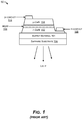
- FIG. 1 is a diagram of an example conventional nitride light emitting diode (LED).
- FIG. 2 is a diagram of an example LED structure suitable for direct-bonding of electrical contacts enabling wafer level, chip array-level, and individual chip-level construction of direct-bonded micro-LED structures.
- FIG. 3 is a diagram of the example LED structure of FIG. 2 , in a direct-bonding operation with driver circuitry.
- FIG. 4 is a diagram of an example process of fabricating the LED structure of FIG. 2 .
- FIG. 5 is a diagram of a first stage of fabricating an example LED array display.
- FIG. 6 is a diagram of a second stage of fabricating the example LED array display.
- FIG. 7 is a diagram of a third stage of fabricating the example LED array display.
- FIG. 8 is a diagram of a fourth stage of fabricating the example LED array display.
- FIG. 9 is a diagram of a fifth stage of fabricating the example LED array display.
- FIG. 10 is a diagram of a completed LED array display and optional components.
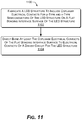
- FIG. 11 is a block diagram of an example process of making a direct-bonded LED structure.
- This disclosure describes example direct-bonded light emitting diode (LED) arrays and applications.
- New processes for forming actively driven mLED (microLED) structures and display cells are described, including example processes of array-bonding III-V compound semiconductor mLEDs to silicon driver chips to form actively driven mLED display cells. Some of these processes may be used to mass-produce mLED array displays.
- FIG. 1 shows an example of a conventional epilayer structure 50 of a light emitting diode (LED) over a sapphire substrate 100 , illustrating and comparing some LED components used in example structures and processes described herein.
- the example conventional LED structure 50 may produce green or blue light, for example.
- Semiconductor materials are layered on a carrier, such as a sapphire substrate 100 .
- the large mismatches in lattice constants and thermal expansion coefficients between GaN and sapphire 100 would cause high crystalline defect densities in the GaN films, which leads to degradation of device performance; hence a lattice and CTE matched buffer material 101 is deposited on sapphire 100 to grow GaN.
- Optoelectronic devices like the conventional LED structure 50 utilize semiconductor doping, for example, a small amount of silicon or germanium is added to gallium nitride (GaN) to make the GaN a conductor for electrons (n-type) n-GaN 102 , and a small amount of magnesium is added to the gallium nitride (GaN) to make the GaN into a conductor for holes (electron holes) (p-type) p-GaN 104 .
- semiconductor doping for example, a small amount of silicon or germanium is added to gallium nitride (GaN) to make the GaN a conductor for electrons (n-type) n-GaN 102 , and a small amount of magnesium is added to the gallium nitride (GaN) to make the GaN into a conductor for holes (electron holes) (p-type) p-GaN 104 .
- n-GaN 102 and the layer of p-GaN 104 are sandwiched an ultrathin layer of a light-producing quantum well or multiple quantum well (MQW) material, that has a smaller band gap (and slightly less conductivity) than either the n-GaN 102 and the p-GaN 104 , such as indium gallium nitride InGaN, a semiconductor material made of a mix of gallium nitride (GaN) and indium nitride (InN). InGaN is a ternary group III/group V direct band gap semiconductor.
- MQW multiple quantum well
- the example InGaN/GaN or InGaN MQW layer 106 provides quantum confinement, or discrete energy subbands, in which the carriers can have only discrete energy values, providing better performance in optical devices.
- Conventional LED structures 50 may have many variations in the number or layers used, and the materials used for each layer. In FIG. 1 , the layers, and especially the MQW layer 106 , are not shown to relative scale.
- the example conventional LED structure 50 is characterized by an n contact 108 and a p contact 110 at different vertical levels on different surfaces of the conventional LED structure 50 .
- the difference in vertical heights between p contact 110 and n contact 108 is conventionally compensated for by wire bond or solder connections.
- an example conventional structure 50 may have an n contact 108 that is not exposed (not shown).
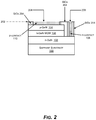
- FIGS. 2-3 show an example LED structure 200 and process overview, for direct-bonding LED components containing III-V semiconductor elements to driver circuitry, for making mLED array displays.
- the example LED structure 200 provides an ultra-flat bonding interface 202 , made flat by chemical-mechanical polishing (CMP) for example, with both n contact 108 and p contact 110 surrounded by an insulator 204 , such as a silicon oxide, and exposed on the ultra-flat bonding interface 202 with respective coplanar conductive footprints 206 & 208 on the ultra-flat bonding interface 202 .
- CMP chemical-mechanical polishing
- contact 108 and p contact 110 may be made of a metal, or combination of alloyed metals, or laminated metals that enhance direct bonding.
- the ultra-flat bonding interface 202 itself also facilitates direct bonding between the n and p contacts 108 & 110 and respective conductive surfaces being bonded to.
- the ultra-flat bonding interface 202 fabricated by damascene methods, for example, is also ultra-clean, and flat within a few tens of nanometers, such as less than 1 ⁇ 4 the wavelength of an illumination source of monochromatic green light at the 546.1 nm or helium-neon red laser light at 632.8 nm.
- the roughness of the flat polished surface 202 is less than 5% of the wavelength of an illumination source and preferably less than 10 nm.
- the flat bonding interface 202 of the LED structure has a first coplanar conductive area 206 and second coplanar conductive area 208 that provide the electrical contacts of the LED element.
- the first 206 and second 208 coplanar conductive areas are within the horizontal footprint of the respective LED element, as represented by the horizontal footprint of the light-producing n-GaN element 102 , which is the illuminated planar area of the LED structure.
- the perimeter of the LED's illuminated area can contiguously touch the illuminated horizontal footprints of each adjacent LED element surrounding it in a direct-bonded LED array, to form a contiguously illuminated surface with no nonilluminated gaps between the LED elements. This forms a contiguously illuminated surface with no gaps between the smallest controllable elements of an image.
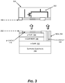
- FIG. 3 shows an example direct-bonding process 300 between the example LED structure 200 of FIG. 2 , and a driver circuit 302 on a chip 304 , to form LED circuitry, such as thin-film transistor (TFT) drivers.
- the example direct-bonding process 300 can be performed at the level of individual chips, or at a chip array level, or at wafer level. For subsequent lift-off and thinning, wafer level direct-bonding may be the best approach.
- the mLED ultra-flat bonding interface 202 can be bonded to the respective ultra-flat bonding interface 306 of a silicon-based driver integrated circuit (IC) 304 , for example.
- the ultra-flat bonding interface 306 may have a contacting surface that is topped with a flat silicon oxide layer and copper (Cu) pads to facilitate direct-bonding, for example direct-bonding via a ZiBond® brand process or a DBI® brand process, to form LED circuitry (Xperi Corporation, San Jose, Calif.).
- the sapphire substrate 100 may then be laser-lifted off. If desirable, both top and bottom sides can be thinned further to make the entire stack flexible.
- FIG. 4 shows stages of example structure fabrication, illustrating an example process flow for making an LED structure 200 suitable for direct-bonding with a silicon driver ICs 304 , for example.
- an example wafer such as a sapphire substrate 100 , is built up with beginning epitaxial layers of n-GaN 102 , InGaN MQW 106 , and p-GaN 104 .
- the top epitaxial layers are patterned and etched to expose the n-GaN layer 102 at specific locations 404 .
- the single exposed location 404 is shown at the edge at the die, there may be more than one location.
- one or more through-vias may expose the n-GaN layer 102 .
- the patterning resist can be left on.
- an insulator or dielectric such as a silicon oxide layer 204 is deposited to cover both the exposed p-GaN 104 and the exposed n-GaN 102 , at least at the location of the contacting pads.
- the silicon oxide layer 204 is patterned and etched over the p-GaN 104 and n-GaN 102 layers to make cavities 410 through the silicon oxide 204 for conductive metals to become the electrodes of the LED structure 200 .
- the total thickness of the p-GaN 104 layer and the MQW 106 layer is approximately 2 ⁇ m, making the structure at this stage suitable for one-step etching and metallization (MQW layer 106 not shown to scale).
- One or more of such cavities 410 can be formed to form one or more electrodes contacting the n-GaN 102 layer and the p-GaN 104 layer.
- the example process deposits a flat silicon oxide layer 204 as in the third stage 406 above, then bonds this oxide surface directly with the driving chip(s) 304 using a ZiBond® brand direct-bonding process, or other direct bonding technique. Then, through-silicon-vias (TSVs) are drilled to create the electrical connectivity from the n contact 108 and the p contact 110 to the driver chip 304 .
- TSVs through-silicon-vias
- the cavities 410 can be metalized with a conductive material 414 .
- barrier and seed layer coatings 416 may be applied and formed, then cavities filled with the conductor 414 , followed by annealing, and chemical-mechanical planarization (CMP).
- CMP chemical-mechanical planarization
- a low melting temperature metal such as indium, may be coated in the cavities.
- a top surface of the example LED structure 200 is plasma-activated 420 for the direct-bonding operation.
- Plasma-activation 420 may be optional for some types of direct-bonding techniques, while in others, the plasma-activation step 420 enhances the bond strength between two metal surfaces, for example, during contact bonding.
- Plasma-activation 420 may also be applied to the opposing surfaces to be bonded on the driver chip(s) 304 .
- the example process flow depicted in FIG. 4 may include picking and transferring many small LED chips with high throughput, and direct-bonding at very fine pitch, for example at a pitch of less than 1 mm (even smaller pitch for making micro-projectors), and at a 0.05 mm spacing, and in various implementations all the way down to a 12 um pitch with 6 um bump.
- the pixel array optics achieve high parallelity of the LED dies 200 to the Si dies 304 .
- Post-processing, such as thinning and laser lift-offs, can be accomplished because the direct-bonding applied results in the flat topography and strong bonding interfaces achieved.
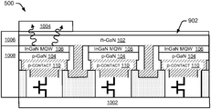
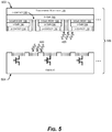
- FIGS. 5-9 show an example process for creating a thin, transparent, and flexible mLED array display 500 , in which a wafer 502 with the LED structures 200 made by the process of FIG. 4 are now bonded to (for example) a CMOS driver chip wafer 504 to make the transparent and flexible array display 500 .
- the CMOS wafer 504 is planarized with CMP or other means of obtaining an ultra-flat surface, and plasma-activated 420 .
- the two wafers 502 & 504 are bonded.
- the first wafer 502 with the LED structures 200 and with coplanar bonding surfaces of the n contacts 108 and p contacts 110 , and the second wafer 504 with CMOS driver chips 304 are brought together for direct-bonding between metallic conductors and in an implementation, between nonmetallic dielectric surfaces 602 also.
- the metal contact pads of the respective wafers 502 & 504 form a metal-to-metal bond during higher-than-room-temperature annealing, as with a DBI® brand direct-bonding process.
- the bonding interface 604 may be annealed at approximately 100-200° C. to form a strong direct bond interface, such as the ZiBond® or DBI® brand direct-bond interface.
- An optical reflective coating such as distributed Bragg reflector (DBR) 606 (not shown to relative scale), can be deposited to increase light output of the package by choosing different types and thickness of the dielectric layers on top of wafer 502 at the interface ( 606 ) between the first wafer 502 and the second wafer 504 .
- the DBR 606 could also be formed on top of the second wafer 504 prior to bonding. In this orientation of a DBR 606 , light can escape from the sapphire side of the device. If DBRs 606 are formed on the first wafer 502 , then the thin dielectrics need to be deposited at the end of the second stage 402 or the third stage 406 of the process shown in FIG. 4 .
- the DBR 606 is a structure formed from multiple layers of alternating materials with varying refractive index, or by periodic variation of some characteristic, for example, thickness of the dielectrics, resulting in periodic variation in the effective refractive index.
- These thin layers of dielectric coatings may be the combination of silicon oxide, magnesium fluoride, tantalum pentoxide, zinc sulfide, and titanium dioxide, for example.
- a silicon oxide SiOx layer on a top surface of the compound wafer 502 can also serve as the last of the coatings which is then bonded directly with direct bonding techniques, such as a ZiBond® or a DBI® process, to wafer 504 .
- DBR may be formed at between sapphire and n-GaN. In this orientation, the light will be reflected towards CMOS wafer 504 . However, less amount of light will escape as CMOS chip would be obstructing the escape route.
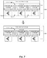
- the thin-film transistor (TFT) backplane can be thinned 702 , which can be facilitated by a ZiBond® brand direct-bonding process. Then the non-transistor parts 704 of the thinned backplane can also be etched away.
- the location of one or more n-contacts 108 and p-contacts 110 can be designed such that they may be exposed from the backside after etching of the backplane; and hence can be contacted for power delivery from the back side.
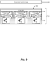
- the thinned and etched transistor surface may be coated with a polyimide (PI) layer 802 or any other dielectric material for protection.
- PI polyimide
- a laser-lift-off of the sapphire substrate layer 100 may be performed, and this exposed side of the wafer 502 then coated with a flexible organic substrate 902 .
- the process to etch and backfill by the transistor backplane by PI may be skipped before a laser-lift-off of the sapphire substrate layer 100 .
- one or more through-electrodes may be needed in the backplane for power delivery to the electrodes.
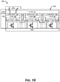
- FIG. 10 shows operational access available on all sides of example transparent and flexible mLED array displays 500 created with direct-bonding.
- This versatility is due at least in part to the strong bonds possible with direct bonding, such as DBI® and ZiBond® brand bonding processes, which result in a final structure able to tolerate further processing on multiple sides of the structure 500 .
- direct bonding such as DBI® and ZiBond® brand bonding processes
- post grinding may be applied and further lift-off performed to make the display thinner, more transparent, and more flexible.
- the backside of the mLED array display 500 may be added onto with backside build-up layers 1002 for further 3D integration to attach to memory, printed circuit boards (PCBs), tactile and other sensors, and so forth.
- PCBs printed circuit boards
- One or more optical waveguides 1004 may be integrated on top of the transparent substrate 902 to transmit optical signals from the LED elements, and also lines for electrical signals may be added.
- the one or more optical waveguides 1004 are attached to the example LED array display 500 by a direct-bonding technique.
- an edge emitting configuration 1006 may be added, and/or optical waveguides on the sides, similar to the one or more optical waveguides 1004 on top.
- reflectors may be needed on both sides of the LED devices 200 , at layer 902 , as well as at the direct-bond (e.g., ZiBond®) interface 604 / 606 .
- the structure of the example mLED array display 500 enables multi-junction stacking of compound semiconductors, for solar cells and solar panels, for example.
- the sides of the example mLED array display 500 can also accommodate cooling structures 1008 .
- the surface may be roughened and indium tin oxide (ITO) added to improve the electrical conductivity of the LEDs.
- ITO indium tin oxide
- the example steps just described and illustrated above provide direct-bonded light emitting diode (LED) arrays 500 , for example arrays of mLEDs, wherein group III-V semiconductor elements are direct-bonded to LED driver circuitry, in wafer-level processes, for example.
- the arrays 500 made through a direct-bonding process, may be flexible, and possess an optically transparent surface.
- the example compound semiconductor-based LED array devices 500 are made with a flat surface composed of coplanar metal regions and dielectric regions.
- the coplanar metal regions are electrically connected to the active regions of the compound semiconductors of each LED element.
- the above compound semiconductor-based LED array structures 500 may include bonds to a CMOS based device connected in a direct-bonding manner.
- the metal regions and the dielectric regions of the compound semiconductor-based LED array device 500 may be bonded directly to the respective metal regions and dielectric regions of the CMOS based device.
- the example process of FIGS. 5-9 can be used not only for wafer-to-wafer (W2W) processes, but also die-to-die (D2D), or one or multiple dies-to-wafer (D2W) processes.
- the resulting example LED array structures 500 may also have other characteristics and features:
- the resulting LED array structures 500 may have an absence of substrate where the group III-V-based semiconductor light-emitting devices are grown. Further, a surface of the microstructure of the group III-V semiconductor-based light-emitting devices can be advantageously roughened for improved light extraction.
- a LED structure is fabricated with electrical contacts to p-type and n-type semiconductor elements coplanar on a first surface comprising a flat bonding interface of the LED structure.
- the first surface is direct-bonded to a second surface comprising a flat bonding interface of a driver circuit for the LED structure.
- the direct-bonding operation used in the example method 1100 may be applied in a wafer level, single chip-level, or a chip array-level process.
- connection In the specification and appended claims: the terms “connect,” “connection,” “connected,” “in connection with,” and “connecting,” are used to mean “in direct connection with” or “in connection with via one or more elements.”
- coupled the terms “couple,” “coupling,” “coupled,” “coupled together,” and “coupled with,” are used to mean “directly coupled together” or “coupled together via one or more elements.”
Landscapes
- Led Devices (AREA)
- Led Device Packages (AREA)
Abstract
Description
Claims (14)
Priority Applications (10)
| Application Number | Priority Date | Filing Date | Title |
|---|---|---|---|
| PCT/US2018/022199 WO2018169968A1 (en) | 2017-03-16 | 2018-03-13 | Direct-bonded led arrays and applications |
| US15/919,570 US10629577B2 (en) | 2017-03-16 | 2018-03-13 | Direct-bonded LED arrays and applications |
| TW107108645A TWI742256B (en) | 2017-03-16 | 2018-03-14 | Direct-bonded led arrays and applications |
| US16/840,245 US11329034B2 (en) | 2017-03-16 | 2020-04-03 | Direct-bonded LED structure contacts and substrate contacts |
| US17/327,169 US11715730B2 (en) | 2017-03-16 | 2021-05-21 | Direct-bonded LED arrays including optical elements configured to transmit optical signals from LED elements |
| US18/206,512 US12166024B2 (en) | 2017-03-16 | 2023-06-06 | Direct-bonded LED arrays drivers |
| US18/498,718 US12199082B2 (en) | 2017-03-16 | 2023-10-31 | Method of direct-bonded optoelectronic devices |
| US18/916,153 US20250038161A1 (en) | 2017-03-16 | 2024-10-15 | Direct-bonded optoelectronic devices |
| US18/977,048 US20250105234A1 (en) | 2017-03-16 | 2024-12-11 | Direct-bonded led arrays and driver circuits |
| US19/353,376 US20260041011A1 (en) | 2017-03-16 | 2025-10-08 | Direct-bonded optoelectronic devices |
Applications Claiming Priority (2)
| Application Number | Priority Date | Filing Date | Title |
|---|---|---|---|
| US201762472363P | 2017-03-16 | 2017-03-16 | |
| US15/919,570 US10629577B2 (en) | 2017-03-16 | 2018-03-13 | Direct-bonded LED arrays and applications |
Related Child Applications (1)
| Application Number | Title | Priority Date | Filing Date |
|---|---|---|---|
| US16/840,245 Continuation US11329034B2 (en) | 2017-03-16 | 2020-04-03 | Direct-bonded LED structure contacts and substrate contacts |
Publications (2)
| Publication Number | Publication Date |
|---|---|
| US20190088633A1 US20190088633A1 (en) | 2019-03-21 |
| US10629577B2 true US10629577B2 (en) | 2020-04-21 |
Family
ID=63522473
Family Applications (8)
| Application Number | Title | Priority Date | Filing Date |
|---|---|---|---|
| US15/919,570 Active US10629577B2 (en) | 2017-03-16 | 2018-03-13 | Direct-bonded LED arrays and applications |
| US16/840,245 Active 2038-06-26 US11329034B2 (en) | 2017-03-16 | 2020-04-03 | Direct-bonded LED structure contacts and substrate contacts |
| US17/327,169 Active 2038-03-23 US11715730B2 (en) | 2017-03-16 | 2021-05-21 | Direct-bonded LED arrays including optical elements configured to transmit optical signals from LED elements |
| US18/206,512 Active US12166024B2 (en) | 2017-03-16 | 2023-06-06 | Direct-bonded LED arrays drivers |
| US18/498,718 Active US12199082B2 (en) | 2017-03-16 | 2023-10-31 | Method of direct-bonded optoelectronic devices |
| US18/916,153 Pending US20250038161A1 (en) | 2017-03-16 | 2024-10-15 | Direct-bonded optoelectronic devices |
| US18/977,048 Pending US20250105234A1 (en) | 2017-03-16 | 2024-12-11 | Direct-bonded led arrays and driver circuits |
| US19/353,376 Pending US20260041011A1 (en) | 2017-03-16 | 2025-10-08 | Direct-bonded optoelectronic devices |
Family Applications After (7)
| Application Number | Title | Priority Date | Filing Date |
|---|---|---|---|
| US16/840,245 Active 2038-06-26 US11329034B2 (en) | 2017-03-16 | 2020-04-03 | Direct-bonded LED structure contacts and substrate contacts |
| US17/327,169 Active 2038-03-23 US11715730B2 (en) | 2017-03-16 | 2021-05-21 | Direct-bonded LED arrays including optical elements configured to transmit optical signals from LED elements |
| US18/206,512 Active US12166024B2 (en) | 2017-03-16 | 2023-06-06 | Direct-bonded LED arrays drivers |
| US18/498,718 Active US12199082B2 (en) | 2017-03-16 | 2023-10-31 | Method of direct-bonded optoelectronic devices |
| US18/916,153 Pending US20250038161A1 (en) | 2017-03-16 | 2024-10-15 | Direct-bonded optoelectronic devices |
| US18/977,048 Pending US20250105234A1 (en) | 2017-03-16 | 2024-12-11 | Direct-bonded led arrays and driver circuits |
| US19/353,376 Pending US20260041011A1 (en) | 2017-03-16 | 2025-10-08 | Direct-bonded optoelectronic devices |
Country Status (3)
| Country | Link |
|---|---|
| US (8) | US10629577B2 (en) |
| TW (1) | TWI742256B (en) |
| WO (1) | WO2018169968A1 (en) |
Cited By (9)
| Publication number | Priority date | Publication date | Assignee | Title |
|---|---|---|---|---|
| WO2021127138A1 (en) | 2019-12-17 | 2021-06-24 | Invensas Bonding Technologies, Inc. | Bonded optical devices |
| US11355480B1 (en) * | 2020-01-27 | 2022-06-07 | Facebook Technologies, Llc | Micropixellation for alignment-free assembly |
| US20230043996A1 (en) * | 2017-12-21 | 2023-02-09 | Lumileds Llc | Led array with light intensity adaptive led sidewalls |
| US12108634B2 (en) | 2020-07-17 | 2024-10-01 | Samsung Display Co., Ltd. | Display device and method of fabricating the same |
| US12199082B2 (en) | 2017-03-16 | 2025-01-14 | Adeia Semiconductor Technologies Llc | Method of direct-bonded optoelectronic devices |
| US12271032B2 (en) | 2018-02-26 | 2025-04-08 | Adeia Semiconductor Bonding Technologies Inc. | Integrated optical waveguides, direct-bonded waveguide interface joints, optical routing and interconnects |
| US12270970B2 (en) | 2018-03-20 | 2025-04-08 | Adeia Semiconductor Bonding Technologies Inc. | Direct-bonded lamination for improved image clarity in optical devices |
| US12336357B2 (en) | 2021-11-24 | 2025-06-17 | Meta Platforms Technologies, Llc | Alignment-free micro-display architecture |
| US12581994B2 (en) | 2017-12-15 | 2026-03-17 | Adeia Semiconductor Bonding Technologies Inc. | Direct-bonded optoelectronic interconnect for high-density integrated photonics |
Families Citing this family (154)
| Publication number | Priority date | Publication date | Assignee | Title |
|---|---|---|---|---|
| US7109092B2 (en) | 2003-05-19 | 2006-09-19 | Ziptronix, Inc. | Method of room temperature covalent bonding |
| US8735219B2 (en) | 2012-08-30 | 2014-05-27 | Ziptronix, Inc. | Heterogeneous annealing method and device |
| US10886250B2 (en) | 2015-07-10 | 2021-01-05 | Invensas Corporation | Structures and methods for low temperature bonding using nanoparticles |
| US9953941B2 (en) | 2015-08-25 | 2018-04-24 | Invensas Bonding Technologies, Inc. | Conductive barrier direct hybrid bonding |
| US10204893B2 (en) | 2016-05-19 | 2019-02-12 | Invensas Bonding Technologies, Inc. | Stacked dies and methods for forming bonded structures |
| US10580735B2 (en) | 2016-10-07 | 2020-03-03 | Xcelsis Corporation | Stacked IC structure with system level wiring on multiple sides of the IC die |
| US10672663B2 (en) | 2016-10-07 | 2020-06-02 | Xcelsis Corporation | 3D chip sharing power circuit |
| US10607136B2 (en) | 2017-08-03 | 2020-03-31 | Xcelsis Corporation | Time borrowing between layers of a three dimensional chip stack |
| TWI822659B (en) | 2016-10-27 | 2023-11-21 | 美商艾德亞半導體科技有限責任公司 | Structures and methods for low temperature bonding |
| US10002844B1 (en) | 2016-12-21 | 2018-06-19 | Invensas Bonding Technologies, Inc. | Bonded structures |
| US20180182665A1 (en) | 2016-12-28 | 2018-06-28 | Invensas Bonding Technologies, Inc. | Processed Substrate |
| WO2018125673A2 (en) | 2016-12-28 | 2018-07-05 | Invensas Bonding Technologies, Inc | Processing stacked substrates |
| TWI837879B (en) | 2016-12-29 | 2024-04-01 | 美商艾德亞半導體接合科技有限公司 | Bonded structures with integrated passive component |
| US10515913B2 (en) | 2017-03-17 | 2019-12-24 | Invensas Bonding Technologies, Inc. | Multi-metal contact structure |
| US10508030B2 (en) | 2017-03-21 | 2019-12-17 | Invensas Bonding Technologies, Inc. | Seal for microelectronic assembly |
| FR3065321B1 (en) * | 2017-04-14 | 2019-06-21 | Commissariat A L'energie Atomique Et Aux Energies Alternatives | METHOD FOR MANUFACTURING EMISSIVE LED DISPLAY DEVICE |
| US10269756B2 (en) | 2017-04-21 | 2019-04-23 | Invensas Bonding Technologies, Inc. | Die processing |
| US10879212B2 (en) | 2017-05-11 | 2020-12-29 | Invensas Bonding Technologies, Inc. | Processed stacked dies |
| US10446441B2 (en) | 2017-06-05 | 2019-10-15 | Invensas Corporation | Flat metal features for microelectronics applications |
| US10217720B2 (en) | 2017-06-15 | 2019-02-26 | Invensas Corporation | Multi-chip modules formed using wafer-level processing of a reconstitute wafer |
| CN111052418A (en) * | 2017-07-31 | 2020-04-21 | 耶鲁大学 | Nanoporous microLED device and method of making the same |
| US10840205B2 (en) | 2017-09-24 | 2020-11-17 | Invensas Bonding Technologies, Inc. | Chemical mechanical polishing for hybrid bonding |
| US11031285B2 (en) | 2017-10-06 | 2021-06-08 | Invensas Bonding Technologies, Inc. | Diffusion barrier collar for interconnects |
| US11380597B2 (en) | 2017-12-22 | 2022-07-05 | Invensas Bonding Technologies, Inc. | Bonded structures |
| WO2019147738A1 (en) * | 2018-01-23 | 2019-08-01 | Light Share, LLC | Full-color monolithic micro-led pixels |
| US10727219B2 (en) | 2018-02-15 | 2020-07-28 | Invensas Bonding Technologies, Inc. | Techniques for processing devices |
| US10991804B2 (en) | 2018-03-29 | 2021-04-27 | Xcelsis Corporation | Transistor level interconnection methodologies utilizing 3D interconnects |
| US11056348B2 (en) | 2018-04-05 | 2021-07-06 | Invensas Bonding Technologies, Inc. | Bonding surfaces for microelectronics |
| US11244916B2 (en) | 2018-04-11 | 2022-02-08 | Invensas Bonding Technologies, Inc. | Low temperature bonded structures |
| US10790262B2 (en) | 2018-04-11 | 2020-09-29 | Invensas Bonding Technologies, Inc. | Low temperature bonded structures |
| US10964664B2 (en) | 2018-04-20 | 2021-03-30 | Invensas Bonding Technologies, Inc. | DBI to Si bonding for simplified handle wafer |
| US11004757B2 (en) | 2018-05-14 | 2021-05-11 | Invensas Bonding Technologies, Inc. | Bonded structures |
| US11276676B2 (en) | 2018-05-15 | 2022-03-15 | Invensas Bonding Technologies, Inc. | Stacked devices and methods of fabrication |
| US10923413B2 (en) | 2018-05-30 | 2021-02-16 | Xcelsis Corporation | Hard IP blocks with physically bidirectional passageways |
| US11393779B2 (en) | 2018-06-13 | 2022-07-19 | Invensas Bonding Technologies, Inc. | Large metal pads over TSV |
| WO2019241417A1 (en) | 2018-06-13 | 2019-12-19 | Invensas Bonding Technologies, Inc. | Tsv as pad |
| US10910344B2 (en) | 2018-06-22 | 2021-02-02 | Xcelsis Corporation | Systems and methods for releveled bump planes for chiplets |
| US11664357B2 (en) | 2018-07-03 | 2023-05-30 | Adeia Semiconductor Bonding Technologies Inc. | Techniques for joining dissimilar materials in microelectronics |
| WO2020010136A1 (en) | 2018-07-06 | 2020-01-09 | Invensas Bonding Technologies, Inc. | Molded direct bonded and interconnected stack |
| WO2020010265A1 (en) | 2018-07-06 | 2020-01-09 | Invensas Bonding Technologies, Inc. | Microelectronic assemblies |
| US12406959B2 (en) | 2018-07-26 | 2025-09-02 | Adeia Semiconductor Bonding Technologies Inc. | Post CMP processing for hybrid bonding |
| US11515291B2 (en) | 2018-08-28 | 2022-11-29 | Adeia Semiconductor Inc. | Integrated voltage regulator and passive components |
| US11296044B2 (en) | 2018-08-29 | 2022-04-05 | Invensas Bonding Technologies, Inc. | Bond enhancement structure in microelectronics for trapping contaminants during direct-bonding processes |
| US11011494B2 (en) | 2018-08-31 | 2021-05-18 | Invensas Bonding Technologies, Inc. | Layer structures for making direct metal-to-metal bonds at low temperatures in microelectronics |
| US11158573B2 (en) | 2018-10-22 | 2021-10-26 | Invensas Bonding Technologies, Inc. | Interconnect structures |
| TWI688317B (en) * | 2018-10-31 | 2020-03-11 | 台灣愛司帝科技股份有限公司 | Led mounted method and device |
| EP3667745B1 (en) | 2018-12-10 | 2023-03-22 | IMEC vzw | Method for obtaining light emitting diodes reconstituted over a carrier substrate |
| EP3667721A1 (en) * | 2018-12-10 | 2020-06-17 | IMEC vzw | Method for fabricating an optical device |
| US11244920B2 (en) | 2018-12-18 | 2022-02-08 | Invensas Bonding Technologies, Inc. | Method and structures for low temperature device bonding |
| JP7348520B2 (en) * | 2018-12-25 | 2023-09-21 | 日亜化学工業株式会社 | Light emitting device and display device |
| KR20210104742A (en) | 2019-01-14 | 2021-08-25 | 인벤사스 본딩 테크놀로지스 인코포레이티드 | junction structure |
| US11355665B2 (en) * | 2019-06-19 | 2022-06-07 | Facebook Technologies, Llc | Process flow for hybrid TFT-based micro display projector |
| US11239399B2 (en) | 2019-02-05 | 2022-02-01 | Facebook Technologies, Llc | Architecture for hybrid TFT-based micro display projector |
| US20220208738A1 (en) * | 2019-02-21 | 2022-06-30 | Vuereal Inc. | Optoelectronic solid state array |
| US11387202B2 (en) | 2019-03-01 | 2022-07-12 | Invensas Llc | Nanowire bonding interconnect for fine-pitch microelectronics |
| US11901281B2 (en) | 2019-03-11 | 2024-02-13 | Adeia Semiconductor Bonding Technologies Inc. | Bonded structures with integrated passive component |
| US10854578B2 (en) | 2019-03-29 | 2020-12-01 | Invensas Corporation | Diffused bitline replacement in stacked wafer memory |
| US11205625B2 (en) | 2019-04-12 | 2021-12-21 | Invensas Bonding Technologies, Inc. | Wafer-level bonding of obstructive elements |
| KR102137688B1 (en) * | 2019-04-12 | 2020-08-28 | 임성규 | Self-Customized Mcro LED Jewelry |
| US11373963B2 (en) | 2019-04-12 | 2022-06-28 | Invensas Bonding Technologies, Inc. | Protective elements for bonded structures |
| US11610846B2 (en) | 2019-04-12 | 2023-03-21 | Adeia Semiconductor Bonding Technologies Inc. | Protective elements for bonded structures including an obstructive element |
| US11355404B2 (en) | 2019-04-22 | 2022-06-07 | Invensas Bonding Technologies, Inc. | Mitigating surface damage of probe pads in preparation for direct bonding of a substrate |
| US11158761B2 (en) | 2019-05-07 | 2021-10-26 | Facebook Technologies, Llc | Bonding methods for light emitting diodes |
| DE102019111816A1 (en) | 2019-05-07 | 2020-11-12 | OSRAM Opto Semiconductors Gesellschaft mit beschränkter Haftung | METHOD OF MANUFACTURING A COMPONENT AND COMPONENT |
| US11385278B2 (en) | 2019-05-23 | 2022-07-12 | Invensas Bonding Technologies, Inc. | Security circuitry for bonded structures |
| US12374641B2 (en) | 2019-06-12 | 2025-07-29 | Adeia Semiconductor Bonding Technologies Inc. | Sealed bonded structures and methods for forming the same |
| JP7341742B2 (en) * | 2019-06-17 | 2023-09-11 | キヤノン株式会社 | light emitting element |
| US11296053B2 (en) | 2019-06-26 | 2022-04-05 | Invensas Bonding Technologies, Inc. | Direct bonded stack structures for increased reliability and improved yield in microelectronics |
| CN110299377B (en) * | 2019-07-03 | 2022-12-16 | 京东方科技集团股份有限公司 | Display substrate, manufacturing method, and display device |
| KR102780352B1 (en) * | 2019-07-05 | 2025-03-12 | 삼성전자주식회사 | Method of manufacturing light emitting device package and method of manufacturing display panel using the same |
| JP2021019015A (en) * | 2019-07-17 | 2021-02-15 | シャープ福山セミコンダクター株式会社 | Micro light emitting element and image display element |
| CN110707148B (en) * | 2019-09-02 | 2021-08-17 | 华南师范大学 | Epitaxial wafer, manufacturing method of epitaxial wafer, diode and rectifier |
| US12080672B2 (en) | 2019-09-26 | 2024-09-03 | Adeia Semiconductor Bonding Technologies Inc. | Direct gang bonding methods including directly bonding first element to second element to form bonded structure without adhesive |
| CN110707186A (en) | 2019-10-21 | 2020-01-17 | 深圳市华星光电半导体显示技术有限公司 | Preparation method of LED display panel |
| US12113054B2 (en) | 2019-10-21 | 2024-10-08 | Adeia Semiconductor Technologies Llc | Non-volatile dynamic random access memory |
| CN112713167B (en) * | 2019-10-25 | 2023-05-19 | 成都辰显光电有限公司 | A kind of display panel and the preparation method of display panel |
| US11862602B2 (en) | 2019-11-07 | 2024-01-02 | Adeia Semiconductor Technologies Llc | Scalable architecture for reduced cycles across SOC |
| WO2021102013A1 (en) * | 2019-11-18 | 2021-05-27 | Avicenatech Corp. | High speed and multi-contact leds for data communication |
| US11296266B2 (en) * | 2019-11-26 | 2022-04-05 | Facebook Technologies, Llc | LED array having transparent substrate with conductive layer for enhanced current spread |
| KR102848957B1 (en) | 2019-11-26 | 2025-08-20 | 삼성전자주식회사 | Semiconductor light emitting device and method of fabricating the same |
| US11876076B2 (en) | 2019-12-20 | 2024-01-16 | Adeia Semiconductor Technologies Llc | Apparatus for non-volatile random access memory stacks |
| CN121793755A (en) | 2019-12-23 | 2026-04-03 | 隔热半导体粘合技术公司 | Electrical redundancy for bonding structures |
| US11721653B2 (en) | 2019-12-23 | 2023-08-08 | Adeia Semiconductor Bonding Technologies Inc. | Circuitry for electrical redundancy in bonded structures |
| CN111226311B (en) | 2020-01-07 | 2021-01-29 | 长江存储科技有限责任公司 | Metal-dielectric bonding methods and structures |
| US11513285B2 (en) | 2020-01-08 | 2022-11-29 | Avicenatech Corp. | Packaging for microLEDs for chip to chip communication |
| US11842989B2 (en) * | 2020-03-10 | 2023-12-12 | Meta Platforms Technologies, Llc | Integrating control circuits with light emissive circuits with dissimilar wafer sizes |
| CN115413368A (en) | 2020-03-18 | 2022-11-29 | 艾维森纳科技有限公司 | LED array for in-plane optical interconnection |
| CN115943489A (en) | 2020-03-19 | 2023-04-07 | 隔热半导体粘合技术公司 | Dimensional Compensation Control for Directly Bonded Structures |
| GB2593699B (en) * | 2020-03-30 | 2022-10-26 | Plessey Semiconductors Ltd | Monolithic LED pixel |
| US11742314B2 (en) | 2020-03-31 | 2023-08-29 | Adeia Semiconductor Bonding Technologies Inc. | Reliable hybrid bonded apparatus |
| US12527137B2 (en) | 2020-04-21 | 2026-01-13 | Raysolve Optoelectronics (Suzhou) Company Limited | Light emitting diode structure and method for manufacturing the same |
| US11817535B2 (en) | 2020-04-21 | 2023-11-14 | Raysolve Optoelectronics (Suzhou) Company Limited | Light emitting diode structure and method for manufacturing the same |
| WO2021217607A1 (en) * | 2020-04-30 | 2021-11-04 | 重庆康佳光电技术研究院有限公司 | Bonding method, display backplate and display backplate manufacturing system |
| US11735523B2 (en) | 2020-05-19 | 2023-08-22 | Adeia Semiconductor Bonding Technologies Inc. | Laterally unconfined structure |
| US11631647B2 (en) | 2020-06-30 | 2023-04-18 | Adeia Semiconductor Bonding Technologies Inc. | Integrated device packages with integrated device die and dummy element |
| WO2022000385A1 (en) * | 2020-07-01 | 2022-01-06 | 重庆康佳光电技术研究院有限公司 | Manufacturing method for display panel, display panel and display device |
| US11728273B2 (en) | 2020-09-04 | 2023-08-15 | Adeia Semiconductor Bonding Technologies Inc. | Bonded structure with interconnect structure |
| US11764177B2 (en) | 2020-09-04 | 2023-09-19 | Adeia Semiconductor Bonding Technologies Inc. | Bonded structure with interconnect structure |
| US11264357B1 (en) | 2020-10-20 | 2022-03-01 | Invensas Corporation | Mixed exposure for large die |
| KR20230097121A (en) | 2020-10-29 | 2023-06-30 | 아데이아 세미컨덕터 본딩 테크놀로지스 인코포레이티드 | Direct bonding method and structure |
| US12456662B2 (en) | 2020-12-28 | 2025-10-28 | Adeia Semiconductor Bonding Technologies Inc. | Structures with through-substrate vias and methods for forming the same |
| WO2022147430A1 (en) | 2020-12-28 | 2022-07-07 | Invensas Bonding Technologies, Inc. | Structures with through-substrate vias and methods for forming the same |
| CN116848631A (en) | 2020-12-30 | 2023-10-03 | 美商艾德亚半导体接合科技有限公司 | Structures with conductive characteristics and methods of forming the same |
| US11710725B2 (en) * | 2021-01-22 | 2023-07-25 | Jade Bird Display (shanghai) Limited | Slicing micro-LED wafer and slicing micro-LED chip |
| DE102021101657B4 (en) * | 2021-01-26 | 2024-12-12 | Infineon Technologies Ag | Method for producing a hybrid component |
| US12525572B2 (en) | 2021-03-31 | 2026-01-13 | Adeia Semiconductor Bonding Technologies Inc. | Direct bonding and debonding of carrier |
| EP4315411A4 (en) | 2021-03-31 | 2025-04-30 | Adeia Semiconductor Bonding Technologies Inc. | DIRECT BONDING METHODS AND STRUCTURES |
| CN113488576A (en) * | 2021-04-13 | 2021-10-08 | 镭昱光电科技(苏州)有限公司 | Light emitting diode structure and manufacturing method thereof |
| CN113270438B (en) * | 2021-04-30 | 2024-02-20 | 广东德力光电有限公司 | Manufacturing process of flip micro LED lattice |
| JP2024528964A (en) | 2021-08-02 | 2024-08-01 | アデイア セミコンダクター ボンディング テクノロジーズ インコーポレイテッド | Protective semiconductor device for bonded structures |
| KR102883717B1 (en) | 2021-08-03 | 2025-11-11 | 삼성전자주식회사 | Display apparatus |
| KR20240059637A (en) | 2021-09-24 | 2024-05-07 | 아데이아 세미컨덕터 본딩 테크놀로지스 인코포레이티드 | Combination structure with active interposer |
| US12604771B2 (en) | 2021-10-28 | 2026-04-14 | Adeia Semiconductor Bonding Technologies Inc. | Direct bonding methods and structures |
| US12563749B2 (en) | 2021-10-28 | 2026-02-24 | Adeia Semiconductor Bonding Technologies Inc | Stacked electronic devices |
| US12557615B2 (en) | 2021-12-13 | 2026-02-17 | Adeia Semiconductor Technologies Llc | Methods for bonding semiconductor elements |
| US12107204B1 (en) | 2021-12-14 | 2024-10-01 | Meta Platforms Technologies, Llc | Small-pitch micro-LEDs |
| JP2025500315A (en) | 2021-12-20 | 2025-01-09 | アデイア セミコンダクター ボンディング テクノロジーズ インコーポレイテッド | Thermoelectric cooling of die packages |
| CN113990765B (en) * | 2021-12-28 | 2023-04-18 | 深圳市思坦科技有限公司 | Preparation method of flexible light-emitting device, flexible light-emitting device and light-emitting device |
| KR20240131388A (en) * | 2021-12-31 | 2024-08-30 | 루미레즈 엘엘씨 | Hybrid bonding for micro light-emitting diode (LED) devices |
| US12512425B2 (en) | 2022-04-25 | 2025-12-30 | Adeia Semiconductor Bonding Technologies Inc. | Expansion controlled structure for direct bonding and method of forming same |
| DE112023001110T5 (en) * | 2022-05-03 | 2025-01-02 | Ams-Osram International Gmbh | METHOD FOR PRODUCING MULTIPLE SEMICONDUCTOR CHIPS AND SEMICONDUCTOR CHIP |
| JP2025517291A (en) | 2022-05-23 | 2025-06-05 | アデイア セミコンダクター ボンディング テクノロジーズ インコーポレイテッド | Testing device for bonded structures |
| US12191233B2 (en) | 2022-07-28 | 2025-01-07 | Adeia Semiconductor Bonding Technologies Inc. | Embedded cooling systems and methods of manufacturing embedded cooling systems |
| US20240097079A1 (en) * | 2022-09-21 | 2024-03-21 | Intel Corporation | Ic package with leds |
| WO2024138186A1 (en) | 2022-12-23 | 2024-06-27 | Adeia Semiconductor Bonding Technologies Inc. | Embedded cooling systems for advanced device packaging |
| CN120457540A (en) | 2022-12-29 | 2025-08-08 | 美商艾德亚半导体接合科技有限公司 | Embedded cooling assembly for advanced device package and method of manufacturing the same |
| US12506114B2 (en) | 2022-12-29 | 2025-12-23 | Adeia Semiconductor Bonding Technologies Inc. | Directly bonded metal structures having aluminum features and methods of preparing same |
| US12545010B2 (en) | 2022-12-29 | 2026-02-10 | Adeia Semiconductor Bonding Technologies Inc. | Directly bonded metal structures having oxide layers therein |
| CN120513517A (en) | 2022-12-31 | 2025-08-19 | 美商艾德亚半导体接合科技有限公司 | Embedded liquid cooling |
| US12341083B2 (en) | 2023-02-08 | 2025-06-24 | Adeia Semiconductor Bonding Technologies Inc. | Electronic device cooling structures bonded to semiconductor elements |
| US12598962B2 (en) | 2023-03-14 | 2026-04-07 | Adeia Semiconductor Bonding Technologies Inc. | System and method for bonding transparent conductor substrates |
| TW202516697A (en) | 2023-03-31 | 2025-04-16 | 美商艾德亞半導體接合科技有限公司 | Integrated cooling assemblies including backside power/ground delivery and methods of manufacturing the same |
| WO2024234298A1 (en) * | 2023-05-16 | 2024-11-21 | Jade Bird Display (shanghai) Limited | Transparent electrode structure for micro led display panel |
| US12191235B2 (en) | 2023-05-17 | 2025-01-07 | Adeia Semiconductor Bonding Technologies Inc. | Integrated cooling assemblies including signal redistribution and methods of manufacturing the same |
| US12191234B2 (en) | 2023-05-17 | 2025-01-07 | Adeia Semiconductor Bonding Technologies Inc. | Integrated cooling assemblies for advanced device packaging and methods of manufacturing the same |
| WO2025091226A1 (en) * | 2023-10-31 | 2025-05-08 | Jade Bird Display (shanghai) Limited | Micro-led array layer and micro-led display panel |
| WO2025096853A1 (en) * | 2023-10-31 | 2025-05-08 | Saphlux, Inc. | Mechanisms for fabricating micro-leds |
| US20250280627A1 (en) * | 2023-11-03 | 2025-09-04 | Google Llc | Methods for led transfer in micro-led displays |
| US12610819B2 (en) | 2023-12-21 | 2026-04-21 | Adeia Semiconductor Bonding Technologies Inc. | Integrated cooling assemblies for advanced device packaging and methods of manufacturing the same |
| US12283490B1 (en) | 2023-12-21 | 2025-04-22 | Adeia Semiconductor Bonding Technologies Inc. | Integrated cooling assemblies for advanced device packaging and methods of manufacturing the same |
| US12368087B2 (en) | 2023-12-26 | 2025-07-22 | Adeia Semiconductor Bonding Technologies Inc. | Embedded cooling systems for advanced device packaging and methods of manufacturing the same |
| US12322677B1 (en) | 2024-02-07 | 2025-06-03 | Adeia Semiconductor Bonding Technologies Inc. | Fluid channel geometry optimizations to improve cooling efficiency |
| US12525506B2 (en) | 2024-02-07 | 2026-01-13 | Adeia Semiconductor Bonding Technologies Inc. | Embedded cooling systems for advanced device packaging and methods of manufacturing the same |
| US12532432B2 (en) | 2024-03-29 | 2026-01-20 | Adeia Semiconductor Bonding Technologies Inc. | Hotspot mitigation in fluid cooling |
| US12336141B1 (en) | 2024-03-29 | 2025-06-17 | Adeia Semiconductor Bonding Technologies Inc. | Cold plate cavity designs for improved thermal performance |
| US12176264B1 (en) | 2024-03-29 | 2024-12-24 | Adeia Semiconductor Bonding Technologies Inc. | Manifold designs for embedded liquid cooling in a package |
| US12500138B2 (en) | 2024-04-17 | 2025-12-16 | Adeia Semiconductor Bonding Technologies Inc. | Cooling channel shape with substantially constant cross sectional area |
| WO2025239839A1 (en) * | 2024-05-17 | 2025-11-20 | New Silicon Corporation Pte Ltd | Pixel chip, display panel, method of fabricating a pixel chip |
| US20250364512A1 (en) * | 2024-05-22 | 2025-11-27 | Adeia Semiconductor Bonding Technologies Inc. | Stacking of optical structures using conductive materials and reflectors |
| US12266545B1 (en) | 2024-05-24 | 2025-04-01 | Adeia Semiconductor Bonding Technologies Inc. | Structures and methods for integrated cold plate in XPUs and memory |
| US20260059905A1 (en) * | 2024-08-22 | 2026-02-26 | Adeia Semiconductor Bonding Technologies Inc. | Optical emitter structures with integrated distributed bragg reflectors |
| US12412808B1 (en) | 2024-12-20 | 2025-09-09 | Adeia Semiconductor Bonding Technologies Inc. | Cold plate and manifold integration for high reliability |
| US12513855B1 (en) | 2025-03-07 | 2025-12-30 | Adeia Semiconductor Bonding Technologies Inc. | Integrated cooling assembly with upper and lower channels |
| CN120435143B (en) * | 2025-07-08 | 2025-10-17 | 杭州芯聚半导体有限公司 | A MicroLED device with a strip-shaped LED light source and a manufacturing method thereof |
Citations (10)
| Publication number | Priority date | Publication date | Assignee | Title |
|---|---|---|---|---|
| US20070096130A1 (en) | 2005-06-09 | 2007-05-03 | Philips Lumileds Lighting Company, Llc | LED Assembly Having Maximum Metal Support for Laser Lift-Off of Growth Substrate |
| US20090009103A1 (en) * | 2007-07-05 | 2009-01-08 | Tyco Electronics Corporation | Wireless controlled light emitting assembly |
| US20100317132A1 (en) | 2009-05-12 | 2010-12-16 | Rogers John A | Printed Assemblies of Ultrathin, Microscale Inorganic Light Emitting Diodes for Deformable and Semitransparent Displays |
| US20110294242A1 (en) | 2009-07-20 | 2011-12-01 | Enerlighting Corp. | Flip-chip gan led fabrication method |
| US20130009183A1 (en) * | 2011-07-08 | 2013-01-10 | Han Chang | Reflective circuit board for led backlight |
| US20130170145A1 (en) * | 2012-01-02 | 2013-07-04 | Tem Products Inc. | Thermal connector |
| US20150021626A1 (en) * | 2012-04-27 | 2015-01-22 | Panasonic Corporation | Light-emitting device |
| US20160141469A1 (en) | 2014-11-18 | 2016-05-19 | Commissariat â l'Energie Atomique et aux Energies Alternatives | Optoelectronic device with light-emitting diodes |
| US20160181477A1 (en) * | 2014-08-27 | 2016-06-23 | Seoul Viosys Co., Ltd. | Light emitting diode and method of fabricating the same |
| US20170148777A1 (en) * | 2015-11-20 | 2017-05-25 | Commissariat A L'energie Atomique Et Aux Energies Alternatives | Optoelectronic device with light-emitting diodes comprising at least one zener diode |
Family Cites Families (431)
| Publication number | Priority date | Publication date | Assignee | Title |
|---|---|---|---|---|
| JPS60257413A (en) | 1984-06-04 | 1985-12-19 | Matsushita Electric Ind Co Ltd | Photoelectric composite device |
| JPH0272642A (en) | 1988-09-07 | 1990-03-12 | Nec Corp | Structure and method for connecting substrates |
| JPH0344067A (en) | 1989-07-11 | 1991-02-25 | Nec Corp | Laminating method of semiconductor substrate |
| US5015052A (en) | 1989-07-20 | 1991-05-14 | Battelle Memorial Institute | Optical modulation at millimeter-wave frequencies |
| CA2083072C (en) | 1991-11-21 | 1998-02-03 | Shinichi Hasegawa | Method for manufacturing polyimide multilayer wiring substrate |
| US6008126A (en) | 1992-04-08 | 1999-12-28 | Elm Technology Corporation | Membrane dielectric isolation IC fabrication |
| US5225797A (en) | 1992-04-27 | 1993-07-06 | Cornell Research Foundation, Inc. | Dielectric waveguide-to-coplanar transmission line transitions |
| KR0137125B1 (en) | 1992-11-16 | 1998-06-15 | 모리시타 요이찌 | Optical waveguide device and manufacturing method |
| US5471090A (en) | 1993-03-08 | 1995-11-28 | International Business Machines Corporation | Electronic structures having a joining geometry providing reduced capacitive loading |
| US5363464A (en) | 1993-06-28 | 1994-11-08 | Tangible Domain Inc. | Dielectric/conductive waveguide |
| JPH07193294A (en) | 1993-11-01 | 1995-07-28 | Matsushita Electric Ind Co Ltd | Electronic component and manufacturing method thereof |
| US5408053A (en) | 1993-11-30 | 1995-04-18 | Hughes Aircraft Company | Layered planar transmission lines |
| US5472914A (en) * | 1994-07-14 | 1995-12-05 | The United States Of America As Represented By The Secretary Of The Air Force | Wafer joined optoelectronic integrated circuits and method |
| KR960009074A (en) | 1994-08-29 | 1996-03-22 | 모리시다 요이치 | Semiconductor device and manufacturing method thereof |
| DE4433330C2 (en) | 1994-09-19 | 1997-01-30 | Fraunhofer Ges Forschung | Method for producing semiconductor structures with advantageous high-frequency properties and a semiconductor wafer structure |
| US5818631A (en) | 1994-11-16 | 1998-10-06 | Raytheon Company | Electrically conducting, directly bonded infrared windows |
| JP3979687B2 (en) | 1995-10-26 | 2007-09-19 | アプライド マテリアルズ インコーポレイテッド | Method for improving film stability of halogen-doped silicon oxide films |
| US6404550B1 (en) | 1996-07-25 | 2002-06-11 | Seiko Epson Corporation | Optical element suitable for projection display apparatus |
| JPH10189671A (en) | 1996-12-24 | 1998-07-21 | Sony Corp | Probing pad structure for semiconductor wafer |
| JP3210889B2 (en) | 1997-01-14 | 2001-09-25 | シャープ株式会社 | Orthogonal dual polarization waveguide input device and satellite broadcast receiving converter using the same |
| US6221753B1 (en) | 1997-01-24 | 2001-04-24 | Micron Technology, Inc. | Flip chip technique for chip assembly |
| GB2315595B (en) | 1997-02-07 | 1998-06-10 | Bookham Technology Ltd | Device for re-directing light fromoptical waveguide |
| JP4032454B2 (en) | 1997-06-27 | 2008-01-16 | ソニー株式会社 | Manufacturing method of three-dimensional circuit element |
| US6097096A (en) | 1997-07-11 | 2000-08-01 | Advanced Micro Devices | Metal attachment method and structure for attaching substrates at low temperatures |
| AU9296098A (en) | 1997-08-29 | 1999-03-16 | Sharon N. Farrens | In situ plasma wafer bonding method |
| JP3307307B2 (en) | 1997-12-19 | 2002-07-24 | 株式会社村田製作所 | Multilayer type high frequency electronic components |
| JP3832076B2 (en) | 1998-02-16 | 2006-10-11 | セイコーエプソン株式会社 | Polarized illumination device and projection display device |
| US6090636A (en) | 1998-02-26 | 2000-07-18 | Micron Technology, Inc. | Integrated circuits using optical waveguide interconnects formed through a semiconductor wafer and methods for forming same |
| US6762796B1 (en) | 1998-08-10 | 2004-07-13 | Olympus Optical Co., Ltd. | Image pickup module having integrated lens and semiconductor chip |
| JP2000100679A (en) | 1998-09-22 | 2000-04-07 | Canon Inc | Micro-region solid-state bonding method between substrates by thinning and device structure |
| JP3532788B2 (en) | 1999-04-13 | 2004-05-31 | 唯知 須賀 | Semiconductor device and manufacturing method thereof |
| US6242324B1 (en) | 1999-08-10 | 2001-06-05 | The United States Of America As Represented By The Secretary Of The Navy | Method for fabricating singe crystal materials over CMOS devices |
| JP2001102479A (en) | 1999-09-27 | 2001-04-13 | Toshiba Corp | Semiconductor integrated circuit device and method of manufacturing the same |
| US6984571B1 (en) | 1999-10-01 | 2006-01-10 | Ziptronix, Inc. | Three dimensional device integration method and integrated device |
| US6801691B2 (en) | 1999-12-23 | 2004-10-05 | Spectalis Corp. | Optical waveguide structures |
| CA2314723A1 (en) | 1999-12-23 | 2001-06-23 | Pierre Simon Joseph Berini | Optical waveguide structures |
| US6614960B2 (en) | 1999-12-23 | 2003-09-02 | Speotalis Corp. | Optical waveguide structures |
| US6300161B1 (en) | 2000-02-15 | 2001-10-09 | Alpine Microsystems, Inc. | Module and method for interconnecting integrated circuits that facilitates high speed signal propagation with reduced noise |
| US6902987B1 (en) | 2000-02-16 | 2005-06-07 | Ziptronix, Inc. | Method for low temperature bonding and bonded structure |
| US6418029B1 (en) | 2000-02-28 | 2002-07-09 | Mckee James S. | Interconnect system having vertically mounted passive components on an underside of a substrate |
| DE10120248A1 (en) | 2000-04-26 | 2002-03-28 | Kyocera Corp | Structure for connecting a non-radiating dielectric waveguide and a metal waveguide, transmitter / receiver module for millimeter waves and transmitter / receiver for millimeter waves |
| US6429532B1 (en) | 2000-05-09 | 2002-08-06 | United Microelectronics Corp. | Pad design |
| JP4322402B2 (en) | 2000-06-22 | 2009-09-02 | 大日本印刷株式会社 | Printed wiring board and manufacturing method thereof |
| AU2001266613A1 (en) | 2000-06-30 | 2002-01-14 | Motorola, Inc. | Integrated circuits with optical interconnect |
| JP3440057B2 (en) | 2000-07-05 | 2003-08-25 | 唯知 須賀 | Semiconductor device and manufacturing method thereof |
| ATE284543T1 (en) | 2000-07-21 | 2004-12-15 | Micro Managed Photons As | TAPE GAP STRUCTURES FOR SURFACE PLASMON POLARITON |
| US6970362B1 (en) | 2000-07-31 | 2005-11-29 | Intel Corporation | Electronic assemblies and systems comprising interposer with embedded capacitors |
| US6423640B1 (en) | 2000-08-09 | 2002-07-23 | Taiwan Semiconductor Manufacturing Co., Ltd. | Headless CMP process for oxide planarization |
| GB2373344A (en) | 2001-03-16 | 2002-09-18 | Bookham Technology Plc | Optical coupling using direct bonding |
| GB2374155A (en) | 2001-03-16 | 2002-10-09 | Bookham Technology Plc | A tapered optical waveguide formed with two substrates |
| US6936854B2 (en) | 2001-05-10 | 2005-08-30 | Canon Kabushiki Kaisha | Optoelectronic substrate |
| US7010183B2 (en) | 2002-03-20 | 2006-03-07 | The Regents Of The University Of Colorado | Surface plasmon devices |
| JP2002353416A (en) | 2001-05-25 | 2002-12-06 | Sony Corp | Semiconductor storage device and method of manufacturing the same |
| JP2003043281A (en) | 2001-07-26 | 2003-02-13 | Kyocera Chemical Corp | Optical wave guide circuit and method for manufacturing the same |
| US20040022691A1 (en) | 2001-08-15 | 2004-02-05 | Allen Susan D. | Method of manufacturing and design of microreactors, including microanalytical and separation devices |
| US6996324B2 (en) | 2001-09-19 | 2006-02-07 | Matsushita Electric Industrial Co., Ltd. | Optical waveguide and method for fabricating the same |
| US20030081906A1 (en) | 2001-10-26 | 2003-05-01 | Filhaber John F. | Direct bonding of optical components |
| US7144827B2 (en) | 2002-01-17 | 2006-12-05 | Silecs Oy | Poly(organosiloxane) materials and methods for hybrid organic-inorganic dielectrics for integrated circuit applications |
| AU2003216067A1 (en) | 2002-01-17 | 2003-09-02 | Silecs Oy | Poly(organosiloxane) materials and methods for hybrid organic-inorganic dielectrics for integrated circuit applications |
| US6759692B1 (en) | 2002-02-04 | 2004-07-06 | Ixys Corporation | Gate driver with level shift circuit |
| US6638808B1 (en) | 2002-02-04 | 2003-10-28 | Ixys Corporation | Method of manufacturing gate driver with level shift circuit |
| US6897492B2 (en) | 2002-02-04 | 2005-05-24 | Ixys Corporation | Power device with bi-directional level shift circuit |
| US6887769B2 (en) | 2002-02-06 | 2005-05-03 | Intel Corporation | Dielectric recess for wafer-to-wafer and die-to-die metal bonding and method of fabricating the same |
| US6762076B2 (en) | 2002-02-20 | 2004-07-13 | Intel Corporation | Process of vertically stacking multiple wafers supporting different active integrated circuit (IC) devices |
| KR100438160B1 (en) | 2002-03-05 | 2004-07-01 | 삼성전자주식회사 | Device having inductor and capacitor and a fabrication method thereof |
| US7832177B2 (en) | 2002-03-22 | 2010-11-16 | Electronics Packaging Solutions, Inc. | Insulated glazing units |
| US6713871B2 (en) | 2002-05-21 | 2004-03-30 | Intel Corporation | Surface mount solder method and apparatus for decoupling capacitance and process of making |
| US7105980B2 (en) | 2002-07-03 | 2006-09-12 | Sawtek, Inc. | Saw filter device and method employing normal temperature bonding for producing desirable filter production and performance characteristics |
| JP4037711B2 (en) | 2002-07-26 | 2008-01-23 | 株式会社東芝 | Semiconductor device having a capacitor formed in an interlayer insulating film |
| JP4083502B2 (en) | 2002-08-19 | 2008-04-30 | 株式会社フジミインコーポレーテッド | Polishing method and polishing composition used therefor |
| US7023093B2 (en) | 2002-10-24 | 2006-04-04 | International Business Machines Corporation | Very low effective dielectric constant interconnect Structures and methods for fabricating the same |
| US7354798B2 (en) | 2002-12-20 | 2008-04-08 | International Business Machines Corporation | Three-dimensional device fabrication method |
| AU2003300348A1 (en) | 2002-12-30 | 2004-07-29 | Corning Incorporated | Fast-switching scalable optical interconnection design with fast contention resolution |
| KR100486303B1 (en) | 2003-02-05 | 2005-04-29 | 삼성전자주식회사 | Flat type capacitor for integrated circuit and method for manufacturing the same |
| US6962835B2 (en) | 2003-02-07 | 2005-11-08 | Ziptronix, Inc. | Method for room temperature metal direct bonding |
| US6908027B2 (en) | 2003-03-31 | 2005-06-21 | Intel Corporation | Complete device layer transfer without edge exclusion via direct wafer bonding and constrained bond-strengthening process |
| JP4235530B2 (en) | 2003-10-20 | 2009-03-11 | キヤノン株式会社 | Surface-emitting diode, surface-emitting diode array, and manufacturing method thereof |
| US7109092B2 (en) | 2003-05-19 | 2006-09-19 | Ziptronix, Inc. | Method of room temperature covalent bonding |
| TWI275168B (en) | 2003-06-06 | 2007-03-01 | Sanyo Electric Co | Semiconductor device and method for making the same |
| JP2005086044A (en) | 2003-09-09 | 2005-03-31 | Citizen Electronics Co Ltd | High reliability package |
| US6979582B2 (en) | 2003-09-22 | 2005-12-27 | National Chung-Hsing University | Vertical-cavity surface emitting laser diode and method for producing the same |
| US7177135B2 (en) | 2003-09-23 | 2007-02-13 | Samsung Electronics Co., Ltd. | On-chip bypass capacitor and method of manufacturing the same |
| US6867073B1 (en) | 2003-10-21 | 2005-03-15 | Ziptronix, Inc. | Single mask via method and device |
| US6943294B2 (en) | 2003-12-22 | 2005-09-13 | Intel Corporation | Integrating passive components on spacer in stacked dies |
| US7132743B2 (en) | 2003-12-23 | 2006-11-07 | Intel Corporation | Integrated circuit package substrate having a thin film capacitor structure |
| JP4260650B2 (en) | 2004-02-26 | 2009-04-30 | 新光電気工業株式会社 | Photoelectric composite substrate and manufacturing method thereof |
| US7842948B2 (en) | 2004-02-27 | 2010-11-30 | Nvidia Corporation | Flip chip semiconductor die internal signal access system and method |
| TW200535878A (en) | 2004-04-16 | 2005-11-01 | Ind Tech Res Inst | Tunable passive device |
| JP4657640B2 (en) | 2004-07-21 | 2011-03-23 | 株式会社日立製作所 | Semiconductor device |
| US20060057945A1 (en) | 2004-09-16 | 2006-03-16 | Chia-Lin Hsu | Chemical mechanical polishing process |
| US20060076634A1 (en) | 2004-09-27 | 2006-04-13 | Lauren Palmateer | Method and system for packaging MEMS devices with incorporated getter |
| US7680464B2 (en) | 2004-12-30 | 2010-03-16 | Valeo Radar Systems, Inc. | Waveguide—printed wiring board (PWB) interconnection |
| GB0505680D0 (en) | 2005-03-22 | 2005-04-27 | Cambridge Display Tech Ltd | Apparatus and method for increased device lifetime in an organic electro-luminescent device |
| JP2006276313A (en) | 2005-03-29 | 2006-10-12 | Kyocera Kinseki Corp | Manufacturing method of optical filter |
| US7355836B2 (en) | 2005-06-07 | 2008-04-08 | Intel Corporation | Array capacitor for decoupling multiple voltage rails |
| JP4572759B2 (en) | 2005-07-06 | 2010-11-04 | セイコーエプソン株式会社 | Semiconductor device and electronic equipment |
| JP2007041117A (en) | 2005-08-01 | 2007-02-15 | Nippon Dempa Kogyo Co Ltd | Laminated optical element and manufacturing method thereof |
| US7485968B2 (en) | 2005-08-11 | 2009-02-03 | Ziptronix, Inc. | 3D IC method and device |
| JP4509972B2 (en) | 2005-09-01 | 2010-07-21 | 日本特殊陶業株式会社 | Wiring board, embedded ceramic chip |
| US7705691B2 (en) | 2005-10-18 | 2010-04-27 | Agency For Science, Technology & Research | Capacitor interconnection |
| KR100735521B1 (en) | 2005-10-19 | 2007-07-04 | 삼성전자주식회사 | Semiconductor device and manufacturing method thereof |
| US7626216B2 (en) | 2005-10-21 | 2009-12-01 | Mckinzie Iii William E | Systems and methods for electromagnetic noise suppression using hybrid electromagnetic bandgap structures |
| IL171820A (en) | 2005-11-08 | 2014-04-30 | Lumus Ltd | Polarizing optical device for light coupling |
| US7193423B1 (en) | 2005-12-12 | 2007-03-20 | International Business Machines Corporation | Wafer-to-wafer alignments |
| TWI305119B (en) | 2005-12-22 | 2009-01-01 | Phoenix Prec Technology Corp | Circuit board structure having capacitance array and embedded electronic component and method for fabricating the same |
| TWI299552B (en) | 2006-03-24 | 2008-08-01 | Advanced Semiconductor Eng | Package structure |
| US7972683B2 (en) | 2006-03-28 | 2011-07-05 | Innovative Micro Technology | Wafer bonding material with embedded conductive particles |
| US8130821B2 (en) | 2006-05-18 | 2012-03-06 | Oracle America, Inc. | Equalization in capacitively coupled communication links |
| US7750488B2 (en) | 2006-07-10 | 2010-07-06 | Tezzaron Semiconductor, Inc. | Method for bonding wafers to produce stacked integrated circuits |
| US7949210B2 (en) | 2006-10-09 | 2011-05-24 | Colorado School Of Mines | Silicon-compatible surface plasmon optical elements |
| US20080124835A1 (en) | 2006-11-03 | 2008-05-29 | International Business Machines Corporation | Hermetic seal and reliable bonding structures for 3d applications |
| EP1936741A1 (en) | 2006-12-22 | 2008-06-25 | Sony Deutschland GmbH | Flexible substrate integrated waveguides |
| US7803693B2 (en) | 2007-02-15 | 2010-09-28 | John Trezza | Bowed wafer hybridization compensation |
| US8558636B2 (en) | 2007-03-30 | 2013-10-15 | Intel Corporation | Package embedded equalizer |
| JP2008258258A (en) | 2007-04-02 | 2008-10-23 | Sanyo Electric Co Ltd | Semiconductor device |
| US7899407B2 (en) | 2007-05-01 | 2011-03-01 | Broadcom Corporation | High frequency signal combining |
| US7867878B2 (en) | 2007-09-21 | 2011-01-11 | Infineon Technologies Ag | Stacked semiconductor chips |
| EP2075850A3 (en) | 2007-12-28 | 2011-08-24 | Semiconductor Energy Laboratory Co, Ltd. | Photoelectric conversion device and manufacturing method thereof |
| US7924113B2 (en) | 2008-02-15 | 2011-04-12 | Realtek Semiconductor Corp. | Integrated front-end passive equalizer and method thereof |
| US8669834B2 (en) | 2008-03-18 | 2014-03-11 | Shi Cheng | Substrate integrated waveguide |
| JP2009239247A (en) | 2008-03-27 | 2009-10-15 | Ibiden Co Ltd | Method of manufacturing multilayer printed circuit board |
| US8009763B2 (en) | 2008-04-02 | 2011-08-30 | Oracle America, Inc. | Method and apparatus for equalizing a high speed serial data link |
| DE112009000987T5 (en) | 2008-04-25 | 2011-03-24 | Hamamatsu Photonics K.K., Hamamatsu | Process for melting glass |
| CN101577686B (en) | 2008-05-09 | 2013-05-08 | 鸿富锦精密工业(深圳)有限公司 | Equalizer and connector provided with same |
| US8349635B1 (en) | 2008-05-20 | 2013-01-08 | Silicon Laboratories Inc. | Encapsulated MEMS device and method to form the same |
| WO2009143462A2 (en) | 2008-05-22 | 2009-11-26 | Vi Systems Gmbh | Method for attaching optical components onto silicon-based integrated circuits |
| US9893004B2 (en) | 2011-07-27 | 2018-02-13 | Broadpak Corporation | Semiconductor interposer integration |
| JP2010103982A (en) | 2008-09-25 | 2010-05-06 | Sony Corp | Millimeter wave transmission device, millimeter wave transmission method, and millimeter wave transmission system |
| US8344503B2 (en) | 2008-11-25 | 2013-01-01 | Freescale Semiconductor, Inc. | 3-D circuits with integrated passive devices |
| JP5195354B2 (en) | 2008-12-01 | 2013-05-08 | セイコーエプソン株式会社 | Optical element |
| KR100945800B1 (en) | 2008-12-09 | 2010-03-05 | 김영혜 | Method for manufacturing heterogeneous bonded wafer |
| US8760342B2 (en) | 2009-03-31 | 2014-06-24 | Kyocera Corporation | Circuit board, high frequency module, and radar apparatus |
| US8476165B2 (en) | 2009-04-01 | 2013-07-02 | Tokyo Electron Limited | Method for thinning a bonding wafer |
| JP2010276940A (en) | 2009-05-29 | 2010-12-09 | Fujifilm Corp | Glass substrate bonding method and glass bonded body |
| US8111730B2 (en) | 2009-08-20 | 2012-02-07 | International Business Machines Corporation | 3D optoelectronic packaging |
| US8482132B2 (en) | 2009-10-08 | 2013-07-09 | International Business Machines Corporation | Pad bonding employing a self-aligned plated liner for adhesion enhancement |
| FR2954585B1 (en) | 2009-12-23 | 2012-03-02 | Soitec Silicon Insulator Technologies | METHOD FOR MAKING A HETEROSTRUCTURE WITH MINIMIZATION OF STRESS |
| US8324622B2 (en) | 2009-12-31 | 2012-12-04 | Stmicroelectronics Inc. | Method of repairing probe pads |
| US8810008B2 (en) | 2010-03-18 | 2014-08-19 | Nec Corporation | Semiconductor element-embedded substrate, and method of manufacturing the substrate |
| US9048112B2 (en) | 2010-06-29 | 2015-06-02 | Qualcomm Incorporated | Integrated voltage regulator with embedded passive device(s) for a stacked IC |
| JP5517800B2 (en) | 2010-07-09 | 2014-06-11 | キヤノン株式会社 | Member for solid-state imaging device and method for manufacturing solid-state imaging device |
| US8461017B2 (en) | 2010-07-19 | 2013-06-11 | Soitec | Methods of forming bonded semiconductor structures using a temporary carrier having a weakened ion implant region for subsequent separation along the weakened region |
| FR2966283B1 (en) | 2010-10-14 | 2012-11-30 | Soi Tec Silicon On Insulator Tech Sa | METHOD FOR PRODUCING A COLLAGE STRUCTURE |
| US9171721B2 (en) | 2010-10-26 | 2015-10-27 | Medtronic, Inc. | Laser assisted direct bonding |
| US8377798B2 (en) | 2010-11-10 | 2013-02-19 | Taiwan Semiconductor Manufacturing Co., Ltd | Method and structure for wafer to wafer bonding in semiconductor packaging |
| US8476146B2 (en) | 2010-12-03 | 2013-07-02 | Taiwan Semiconductor Manufacturing Company, Ltd. | Reducing wafer distortion through a low CTE layer |
| KR101141457B1 (en) | 2010-12-08 | 2012-05-04 | 삼성전기주식회사 | The multi-layerd ceramic condenser and fabricating method using thereof |
| TWI405322B (en) | 2010-12-29 | 2013-08-11 | 財團法人工業技術研究院 | Built-in capacitor substrate module |
| CA2823806C (en) | 2011-01-10 | 2017-08-29 | Universite Laval | Laser reinforced direct bonding of optical components |
| FR2970594B1 (en) | 2011-01-13 | 2013-01-18 | Batscap Sa | ELECTRIC ENERGY STORAGE ASSEMBLY WITH ACCORDIED STACKING ELEMENT |
| US8620164B2 (en) | 2011-01-20 | 2013-12-31 | Intel Corporation | Hybrid III-V silicon laser formed by direct bonding |
| US8988299B2 (en) | 2011-02-17 | 2015-03-24 | International Business Machines Corporation | Integrated antenna for RFIC package applications |
| US8686537B2 (en) | 2011-03-03 | 2014-04-01 | Skyworks Solutions, Inc. | Apparatus and methods for reducing impact of high RF loss plating |
| US9160346B2 (en) | 2011-03-15 | 2015-10-13 | Rambus Inc. | Area and power efficient clock generation |
| US8716105B2 (en) | 2011-03-31 | 2014-05-06 | Soitec | Methods for bonding semiconductor structures involving annealing processes, and bonded semiconductor structures and intermediate structures formed using such methods |
| US8501537B2 (en) | 2011-03-31 | 2013-08-06 | Soitec | Methods for bonding semiconductor structures involving annealing processes, and bonded semiconductor structures formed using such methods |
| JP2012226000A (en) | 2011-04-15 | 2012-11-15 | Seiko Epson Corp | Optical element, projection type video apparatus and method for manufacturing optical element |
| JP2012226121A (en) | 2011-04-20 | 2012-11-15 | Seiko Epson Corp | Polarization conversion element, polarization conversion unit, and projection device |
| CN102768450B (en) | 2011-05-03 | 2014-10-29 | 中国科学院理化技术研究所 | KBBF group crystal and prism coupled optical coupling device and preparation method thereof |
| KR101952976B1 (en) | 2011-05-24 | 2019-02-27 | 소니 주식회사 | Semiconductor device |
| JP2012247705A (en) | 2011-05-30 | 2012-12-13 | Seiko Epson Corp | Polarization conversion element, polarization conversion unit, and projection type video device |
| JP5982748B2 (en) | 2011-08-01 | 2016-08-31 | ソニー株式会社 | SEMICONDUCTOR DEVICE, SEMICONDUCTOR DEVICE MANUFACTURING METHOD, AND ELECTRONIC DEVICE |
| WO2013009711A1 (en) | 2011-07-08 | 2013-01-17 | Timler John P | Insulator based upon one or more dielectric structures |
| US8697493B2 (en) | 2011-07-18 | 2014-04-15 | Soitec | Bonding surfaces for direct bonding of semiconductor structures |
| US8441087B2 (en) | 2011-07-22 | 2013-05-14 | Raytheon Company | Direct readout focal plane array |
| US8441131B2 (en) | 2011-09-12 | 2013-05-14 | Globalfoundries Inc. | Strain-compensating fill patterns for controlling semiconductor chip package interactions |
| US8436457B2 (en) | 2011-10-03 | 2013-05-07 | Invensas Corporation | Stub minimization for multi-die wirebond assemblies with parallel windows |
| US8441111B2 (en) | 2011-10-03 | 2013-05-14 | Invensas Corporation | Stub minimization for multi-die wirebond assemblies with parallel windows |
| TWI438882B (en) | 2011-11-01 | 2014-05-21 | 欣興電子股份有限公司 | Package substrate with embedded capacitor element and method of manufacturing same |
| JP5703206B2 (en) | 2011-12-19 | 2015-04-15 | 株式会社日立製作所 | Semiconductor device, signal transmission system, and signal transmission method |
| US9274338B2 (en) | 2012-03-21 | 2016-03-01 | Microsoft Technology Licensing, Llc | Increasing field of view of reflective waveguide |
| US20130265733A1 (en) | 2012-04-04 | 2013-10-10 | Texas Instruments Incorporated | Interchip communication using an embedded dielectric waveguide |
| CN103377911B (en) | 2012-04-16 | 2016-09-21 | 中国科学院微电子研究所 | Method for Improving Uniformity of Chemical Mechanical Planarization Process |
| US9142517B2 (en) | 2012-06-05 | 2015-09-22 | Taiwan Semiconductor Manufacturing Company, Ltd. | Hybrid bonding mechanisms for semiconductor wafers |
| US8809123B2 (en) | 2012-06-05 | 2014-08-19 | Taiwan Semiconductor Manufacturing Company, Ltd. | Three dimensional integrated circuit structures and hybrid bonding methods for semiconductor wafers |
| US8698323B2 (en) | 2012-06-18 | 2014-04-15 | Invensas Corporation | Microelectronic assembly tolerant to misplacement of microelectronic elements therein |
| US9502424B2 (en) | 2012-06-29 | 2016-11-22 | Qualcomm Incorporated | Integrated circuit device featuring an antifuse and method of making same |
| US9036952B2 (en) | 2012-07-25 | 2015-05-19 | International Business Machines Corporation | Electro-optical assembly for silicon photonic chip and electro-optical carrier |
| TWI497661B (en) | 2012-08-15 | 2015-08-21 | 財團法人工業技術研究院 | Semiconductor substrate |
| US9343393B2 (en) | 2012-08-15 | 2016-05-17 | Industrial Technology Research Institute | Semiconductor substrate assembly with embedded resistance element |
| US8829673B2 (en) | 2012-08-17 | 2014-09-09 | Taiwan Semiconductor Manufacturing Company, Ltd. | Bonded structures for package and substrate |
| KR101977699B1 (en) | 2012-08-20 | 2019-08-28 | 에스케이하이닉스 주식회사 | Multi chip semiconductor apparatus and method of testing the same |
| US8735219B2 (en) | 2012-08-30 | 2014-05-27 | Ziptronix, Inc. | Heterogeneous annealing method and device |
| KR101420517B1 (en) | 2012-10-31 | 2014-07-16 | 삼성전기주식회사 | Multi-Layer Ceramic Capacitor and Printed Circuit Board embedding the same |
| US9434145B2 (en) | 2012-12-07 | 2016-09-06 | Semrock, Inc. | Dichroic filter conformed to optical surface |
| US9773824B2 (en) * | 2012-12-13 | 2017-09-26 | Cbrite Inc. | Active matrix light emitting diode array and projector display comprising it |
| DE102012224310A1 (en) | 2012-12-21 | 2014-06-26 | Tesa Se | Gettermaterial containing adhesive tape |
| US20140175655A1 (en) | 2012-12-22 | 2014-06-26 | Industrial Technology Research Institute | Chip bonding structure and manufacturing method thereof |
| TWI479640B (en) | 2012-12-25 | 2015-04-01 | 財團法人工業技術研究院 | Wafer stack structure |
| KR101375938B1 (en) | 2012-12-27 | 2014-03-21 | 한국과학기술원 | Low power, high speed multi-channel chip-to-chip interface using dielectric waveguide |
| US8916448B2 (en) | 2013-01-09 | 2014-12-23 | International Business Machines Corporation | Metal to metal bonding for stacked (3D) integrated circuits |
| TWI518991B (en) | 2013-02-08 | 2016-01-21 | 巽晨國際股份有限公司 | Integrated antenna and integrated circuit components of the shielding module |
| US8946784B2 (en) | 2013-02-18 | 2015-02-03 | Taiwan Semiconductor Manufacturing Company, Ltd. | Method and apparatus for image sensor packaging |
| JP5934424B2 (en) | 2013-02-19 | 2016-06-15 | 日本碍子株式会社 | Manufacturing method of acoustic wave device |
| US9263186B2 (en) | 2013-03-05 | 2016-02-16 | Qualcomm Incorporated | DC/ AC dual function Power Delivery Network (PDN) decoupling capacitor |
| US9105485B2 (en) | 2013-03-08 | 2015-08-11 | Taiwan Semiconductor Manufacturing Company, Ltd. | Bonding structures and methods of forming the same |
| US9029983B2 (en) | 2013-03-12 | 2015-05-12 | Qualcomm Incorporated | Metal-insulator-metal (MIM) capacitor |
| DE102013102667A1 (en) * | 2013-03-15 | 2014-10-02 | Osram Opto Semiconductors Gmbh | display device |
| US9443796B2 (en) | 2013-03-15 | 2016-09-13 | Taiwan Semiconductor Manufacturing Company, Ltd. | Air trench in packages incorporating hybrid bonding |
| US8802538B1 (en) | 2013-03-15 | 2014-08-12 | Taiwan Semiconductor Manufacturing Company, Ltd. | Methods for hybrid wafer bonding |
| GB2512379A (en) | 2013-03-28 | 2014-10-01 | Ibm | Photonic and/or optoelectronic packaging assembly |
| US9064937B2 (en) | 2013-05-30 | 2015-06-23 | International Business Machines Corporation | Substrate bonding with diffusion barrier structures |
| US9929050B2 (en) | 2013-07-16 | 2018-03-27 | Taiwan Semiconductor Manufacturing Company, Ltd. | Mechanisms for forming three-dimensional integrated circuit (3DIC) stacking structure |
| US9723716B2 (en) | 2013-09-27 | 2017-08-01 | Infineon Technologies Ag | Contact pad structure, an electronic component, and a method for manufacturing a contact pad structure |
| JP6287037B2 (en) | 2013-10-16 | 2018-03-07 | セイコーエプソン株式会社 | Polarization conversion element, projector, and method of manufacturing polarization conversion element |
| US9257399B2 (en) | 2013-10-17 | 2016-02-09 | Taiwan Semiconductor Manufacturing Company, Ltd. | 3D integrated circuit and methods of forming the same |
| JP6221668B2 (en) | 2013-11-18 | 2017-11-01 | 日亜化学工業株式会社 | Manufacturing method of light distribution member and manufacturing method of light emitting device |
| JP2015115446A (en) | 2013-12-11 | 2015-06-22 | 株式会社東芝 | Manufacturing method of semiconductor device |
| US9437572B2 (en) | 2013-12-18 | 2016-09-06 | Taiwan Semiconductor Manufacturing Company, Ltd. | Conductive pad structure for hybrid bonding and methods of forming same |
| JP2015119072A (en) | 2013-12-19 | 2015-06-25 | 富士電機株式会社 | Laser welding method, laser welding jig, semiconductor device |
| US9508637B2 (en) | 2014-01-06 | 2016-11-29 | Taiwan Semiconductor Manufacturing Company, Ltd. | Protrusion bump pads for bond-on-trace processing |
| US10090327B2 (en) | 2014-01-17 | 2018-10-02 | Taiwan Semiconductor Manufacturing Co., Ltd | Semiconductor device and method for forming the same |
| US9472479B2 (en) | 2014-01-31 | 2016-10-18 | Corning Incorporated | Methods and apparatus for providing an interposer for interconnecting semiconductor chips |
| US20150262902A1 (en) | 2014-03-12 | 2015-09-17 | Invensas Corporation | Integrated circuits protected by substrates with cavities, and methods of manufacture |
| US9418924B2 (en) | 2014-03-20 | 2016-08-16 | Invensas Corporation | Stacked die integrated circuit |
| US9230941B2 (en) | 2014-03-28 | 2016-01-05 | Taiwan Semiconductor Manufacturing Company, Ltd. | Bonding structure for stacked semiconductor devices |
| US9299736B2 (en) | 2014-03-28 | 2016-03-29 | Taiwan Semiconductor Manufacturing Company, Ltd. | Hybrid bonding with uniform pattern density |
| US9853361B2 (en) | 2014-05-02 | 2017-12-26 | The Invention Science Fund I Llc | Surface scattering antennas with lumped elements |
| US9472458B2 (en) | 2014-06-04 | 2016-10-18 | Semiconductor Components Industries, Llc | Method of reducing residual contamination in singulated semiconductor die |
| TWI814461B (en) * | 2014-06-18 | 2023-09-01 | 愛爾蘭商艾克斯展示公司技術有限公司 | Micro assembled led displays and lighting elements |
| KR102275705B1 (en) | 2014-07-11 | 2021-07-09 | 삼성전자주식회사 | Wafer-to-wafer bonding structure |
| US20170207600A1 (en) | 2014-07-14 | 2017-07-20 | Biond Photonics Inc. | 3d photonic integration with light coupling elements |
| GB201413578D0 (en) | 2014-07-31 | 2014-09-17 | Infiniled Ltd | A colour iled display on silicon |
| US9772463B2 (en) | 2014-09-04 | 2017-09-26 | International Business Machines Corporation | Intra chip optical interconnect structure |
| US9372316B2 (en) | 2014-09-11 | 2016-06-21 | Taiwan Semiconductor Manufacturing Co., Ltd. | Silicon interface for dielectric slab waveguide |
| US9671572B2 (en) | 2014-09-22 | 2017-06-06 | Oracle International Corporation | Integrated chip package with optical interface |
| US20160097930A1 (en) | 2014-10-06 | 2016-04-07 | Steven John Robbins | Microdisplay optical system having two microlens arrays |
| US9536848B2 (en) | 2014-10-16 | 2017-01-03 | Globalfoundries Inc. | Bond pad structure for low temperature flip chip bonding |
| US9423563B2 (en) | 2014-10-20 | 2016-08-23 | International Business Machines Corporation | Variable buried oxide thickness for a waveguide |
| US10018788B2 (en) | 2014-10-28 | 2018-07-10 | Hewlett Packard Enterprise Development Lp | Photonic interposer with wafer bonded microlenses |
| US9394161B2 (en) | 2014-11-14 | 2016-07-19 | Taiwan Semiconductor Manufacturing Co., Ltd. | MEMS and CMOS integration with low-temperature bonding |
| DE102014117723B4 (en) | 2014-12-02 | 2019-01-24 | Infineon Technologies Ag | Semiconductor device and method of manufacturing a semiconductor device |
| US9899442B2 (en) | 2014-12-11 | 2018-02-20 | Invensas Corporation | Image sensor device |
| KR101793967B1 (en) | 2014-12-24 | 2017-11-06 | 인텔 코포레이션 | Integrated passive components in a stacked integrated circuit package |
| JP2016143853A (en) | 2015-02-05 | 2016-08-08 | 富士通株式会社 | Layered semiconductor device |
| US20160254345A1 (en) | 2015-02-27 | 2016-09-01 | Globalfoundries Inc. | Metal-insulator-metal capacitor architecture |
| US9537199B2 (en) | 2015-03-19 | 2017-01-03 | International Business Machines Corporation | Package structure having an integrated waveguide configured to communicate between first and second integrated circuit chips |
| US20160291269A1 (en) | 2015-04-01 | 2016-10-06 | Coriant Advanced Technology, LLC | Photonic integrated circuit chip packaging |
| EP3281056A1 (en) * | 2015-04-10 | 2018-02-14 | Essilor International | Head mounted display device |
| KR101681410B1 (en) | 2015-04-20 | 2016-11-30 | 삼성전기주식회사 | Capacitor Component |
| DE102015108545A1 (en) * | 2015-05-29 | 2016-12-01 | Osram Opto Semiconductors Gmbh | Optoelectronic component and method for producing an optoelectronic component |
| US9741620B2 (en) | 2015-06-24 | 2017-08-22 | Invensas Corporation | Structures and methods for reliable packages |
| US9656852B2 (en) | 2015-07-06 | 2017-05-23 | Taiwan Semiconductor Manufacturing Company Ltd. | CMOS-MEMS device structure, bonding mesa structure and associated method |
| US10886250B2 (en) | 2015-07-10 | 2021-01-05 | Invensas Corporation | Structures and methods for low temperature bonding using nanoparticles |
| WO2017011267A1 (en) | 2015-07-15 | 2017-01-19 | Dueweke Michael J | Tunable reactance devices, and methods of making and using the same |
| US10075657B2 (en) | 2015-07-21 | 2018-09-11 | Fermi Research Alliance, Llc | Edgeless large area camera system |
| US9786715B2 (en) | 2015-07-23 | 2017-10-10 | Artilux Corporation | High efficiency wide spectrum sensor |
| US9728521B2 (en) | 2015-07-23 | 2017-08-08 | Taiwan Semiconductor Manufacturing Co., Ltd. | Hybrid bond using a copper alloy for yield improvement |
| US9786641B2 (en) | 2015-08-13 | 2017-10-10 | International Business Machines Corporation | Packaging optoelectronic components and CMOS circuitry using silicon-on-insulator substrates for photonics applications |
| US9559081B1 (en) | 2015-08-21 | 2017-01-31 | Apple Inc. | Independent 3D stacking |
| US9627373B2 (en) | 2015-08-25 | 2017-04-18 | International Business Machines Corporation | CMOS compatible fuse or resistor using self-aligned contacts |
| US9953941B2 (en) | 2015-08-25 | 2018-04-24 | Invensas Bonding Technologies, Inc. | Conductive barrier direct hybrid bonding |
| US10177127B2 (en) * | 2015-09-04 | 2019-01-08 | Hong Kong Beida Jade Bird Display Limited | Semiconductor apparatus and method of manufacturing the same |
| FR3044467B1 (en) | 2015-11-26 | 2018-08-10 | Commissariat A L'energie Atomique Et Aux Energies Alternatives | LIGHT DALLE AND METHOD FOR MANUFACTURING SUCH LIGHT SLAB |
| US9496239B1 (en) | 2015-12-11 | 2016-11-15 | International Business Machines Corporation | Nitride-enriched oxide-to-oxide 3D wafer bonding |
| US9852988B2 (en) | 2015-12-18 | 2017-12-26 | Invensas Bonding Technologies, Inc. | Increased contact alignment tolerance for direct bonding |
| US20170186730A1 (en) | 2015-12-26 | 2017-06-29 | Invensas Corporation | System and method for providing 3d wafer assembly with known-good-dies |
| US9881882B2 (en) | 2016-01-06 | 2018-01-30 | Mediatek Inc. | Semiconductor package with three-dimensional antenna |
| US9923011B2 (en) | 2016-01-12 | 2018-03-20 | Taiwan Semiconductor Manufacturing Co., Ltd. | Semiconductor device structure with stacked semiconductor dies |
| US10446532B2 (en) | 2016-01-13 | 2019-10-15 | Invensas Bonding Technologies, Inc. | Systems and methods for efficient transfer of semiconductor elements |
| US10636767B2 (en) | 2016-02-29 | 2020-04-28 | Invensas Corporation | Correction die for wafer/die stack |
| JP2017177519A (en) | 2016-03-30 | 2017-10-05 | 株式会社トプコン | Member joining method and optical element produced by the method |
| US10026716B2 (en) | 2016-04-15 | 2018-07-17 | Taiwan Semiconductor Manufacturing Company, Ltd. | 3DIC formation with dies bonded to formed RDLs |
| KR102601055B1 (en) | 2016-05-10 | 2023-11-09 | 삼성전자주식회사 | Compound and organic photoelectric device, image sensor and electronic device including the same |
| US9806059B1 (en) | 2016-05-12 | 2017-10-31 | Taiwan Semiconductor Manufacturing Company, Ltd. | Multi-stack package-on-package structures |
| US10204893B2 (en) | 2016-05-19 | 2019-02-12 | Invensas Bonding Technologies, Inc. | Stacked dies and methods for forming bonded structures |
| US10522400B2 (en) | 2016-05-27 | 2019-12-31 | Taiwan Semiconductor Manufacturing Co., Ltd. | Embedded temperature control system for a biosensor |
| KR102505856B1 (en) | 2016-06-09 | 2023-03-03 | 삼성전자 주식회사 | wafer-to-wafer bonding structure |
| US9941241B2 (en) | 2016-06-30 | 2018-04-10 | International Business Machines Corporation | Method for wafer-wafer bonding |
| CN106206872A (en) | 2016-08-04 | 2016-12-07 | 南京大学 | GaN base visible ray micron post array LED device that Si CMOS array drive circuit controls and preparation method thereof |
| US9892961B1 (en) | 2016-08-09 | 2018-02-13 | International Business Machines Corporation | Air gap spacer formation for nano-scale semiconductor devices |
| US10446487B2 (en) | 2016-09-30 | 2019-10-15 | Invensas Bonding Technologies, Inc. | Interface structures and methods for forming same |
| US10672663B2 (en) | 2016-10-07 | 2020-06-02 | Xcelsis Corporation | 3D chip sharing power circuit |
| US10607136B2 (en) | 2017-08-03 | 2020-03-31 | Xcelsis Corporation | Time borrowing between layers of a three dimensional chip stack |
| US10580735B2 (en) | 2016-10-07 | 2020-03-03 | Xcelsis Corporation | Stacked IC structure with system level wiring on multiple sides of the IC die |
| US10690917B2 (en) | 2016-10-31 | 2020-06-23 | Tectus Corporation | Femtoprojector optical systems, used in eye-mounted display |
| US11287563B2 (en) | 2016-12-01 | 2022-03-29 | Ostendo Technologies, Inc. | Polarized light emission from micro-pixel displays and methods of fabrication thereof |
| US10163750B2 (en) | 2016-12-05 | 2018-12-25 | Taiwan Semiconductor Manufacturing Company, Ltd. | Package structure for heat dissipation |
| EP3557293A4 (en) | 2016-12-13 | 2020-08-05 | NGK Insulators, Ltd. | OPTICAL COMPONENT |
| US10453832B2 (en) | 2016-12-15 | 2019-10-22 | Taiwan Semiconductor Manufacturing Co., Ltd. | Seal ring structures and methods of forming same |
| US10002844B1 (en) | 2016-12-21 | 2018-06-19 | Invensas Bonding Technologies, Inc. | Bonded structures |
| US20180182665A1 (en) | 2016-12-28 | 2018-06-28 | Invensas Bonding Technologies, Inc. | Processed Substrate |
| WO2018125673A2 (en) | 2016-12-28 | 2018-07-05 | Invensas Bonding Technologies, Inc | Processing stacked substrates |
| TWI837879B (en) | 2016-12-29 | 2024-04-01 | 美商艾德亞半導體接合科技有限公司 | Bonded structures with integrated passive component |
| US20180190583A1 (en) | 2016-12-29 | 2018-07-05 | Invensas Bonding Technologies, Inc. | Bonded structures with integrated passive component |
| US10276909B2 (en) | 2016-12-30 | 2019-04-30 | Invensas Bonding Technologies, Inc. | Structure comprising at least a first element bonded to a carrier having a closed metallic channel waveguide formed therein |
| US10431614B2 (en) | 2017-02-01 | 2019-10-01 | Semiconductor Components Industries, Llc | Edge seals for semiconductor packages |
| JP7030825B2 (en) | 2017-02-09 | 2022-03-07 | インヴェンサス ボンディング テクノロジーズ インコーポレイテッド | Joined structure |
| TWI631726B (en) * | 2017-03-10 | 2018-08-01 | 錼創科技股份有限公司 | Light-emitting element and display device |
| US10629577B2 (en) | 2017-03-16 | 2020-04-21 | Invensas Corporation | Direct-bonded LED arrays and applications |
| US10515913B2 (en) | 2017-03-17 | 2019-12-24 | Invensas Bonding Technologies, Inc. | Multi-metal contact structure |
| CN110462850B (en) | 2017-03-20 | 2024-04-16 | 上海显耀显示科技有限公司 | Semiconductor devices are made by stacking layers of micro-LEDs |
| CN110709772B (en) | 2017-03-21 | 2022-06-21 | 奇跃公司 | Method, apparatus and system for illuminating a spatial light modulator |
| US10508030B2 (en) | 2017-03-21 | 2019-12-17 | Invensas Bonding Technologies, Inc. | Seal for microelectronic assembly |
| JP6640780B2 (en) | 2017-03-22 | 2020-02-05 | キオクシア株式会社 | Semiconductor device manufacturing method and semiconductor device |
| US10840223B2 (en) | 2017-03-23 | 2020-11-17 | Intel Corporation | Augmented reality display systems with super-lambertian LED source |
| WO2018183739A1 (en) | 2017-03-31 | 2018-10-04 | Invensas Bonding Technologies, Inc. | Interface structures and methods for forming same |
| US10269756B2 (en) | 2017-04-21 | 2019-04-23 | Invensas Bonding Technologies, Inc. | Die processing |
| US10580823B2 (en) | 2017-05-03 | 2020-03-03 | United Microelectronics Corp. | Wafer level packaging method |
| US10879212B2 (en) | 2017-05-11 | 2020-12-29 | Invensas Bonding Technologies, Inc. | Processed stacked dies |
| US10529634B2 (en) | 2017-05-11 | 2020-01-07 | Invensas Bonding Technologies, Inc. | Probe methodology for ultrafine pitch interconnects |
| JP6966691B2 (en) | 2017-05-31 | 2021-11-17 | 日亜化学工業株式会社 | Light emitting device and manufacturing method of light emitting device |
| WO2018223150A1 (en) | 2017-06-01 | 2018-12-06 | Pogotec Inc. | Releasably attachable augmented reality system for eyewear |
| US10446441B2 (en) | 2017-06-05 | 2019-10-15 | Invensas Corporation | Flat metal features for microelectronics applications |
| US11422369B1 (en) | 2017-06-14 | 2022-08-23 | Meta Platforms Technologies, Llc | Multi-layered substrates for waveguide displays |
| US10217720B2 (en) | 2017-06-15 | 2019-02-26 | Invensas Corporation | Multi-chip modules formed using wafer-level processing of a reconstitute wafer |
| US10707374B2 (en) | 2017-09-15 | 2020-07-07 | Glo Ab | Etendue enhancement for light emitting diode subpixels |
| US10840205B2 (en) | 2017-09-24 | 2020-11-17 | Invensas Bonding Technologies, Inc. | Chemical mechanical polishing for hybrid bonding |
| US11195748B2 (en) | 2017-09-27 | 2021-12-07 | Invensas Corporation | Interconnect structures and methods for forming same |
| US11031285B2 (en) | 2017-10-06 | 2021-06-08 | Invensas Bonding Technologies, Inc. | Diffusion barrier collar for interconnects |
| US11251157B2 (en) | 2017-11-01 | 2022-02-15 | Taiwan Semiconductor Manufacturing Company, Ltd. | Die stack structure with hybrid bonding structure and method of fabricating the same and package |
| US11011503B2 (en) | 2017-12-15 | 2021-05-18 | Invensas Bonding Technologies, Inc. | Direct-bonded optoelectronic interconnect for high-density integrated photonics |
| US11380597B2 (en) | 2017-12-22 | 2022-07-05 | Invensas Bonding Technologies, Inc. | Bonded structures |
| US10923408B2 (en) | 2017-12-22 | 2021-02-16 | Invensas Bonding Technologies, Inc. | Cavity packages |
| US10942355B2 (en) | 2018-01-22 | 2021-03-09 | Facebook Technologies, Llc | Systems, devices, and methods for tiled multi-monochromatic displays |
| US10739595B2 (en) | 2018-01-22 | 2020-08-11 | Facebook Technologies, Llc | Application specific integrated circuit for waveguide display |
| US11127738B2 (en) | 2018-02-09 | 2021-09-21 | Xcelsis Corporation | Back biasing of FD-SOI circuit blocks |
| US10727219B2 (en) | 2018-02-15 | 2020-07-28 | Invensas Bonding Technologies, Inc. | Techniques for processing devices |
| US11169326B2 (en) | 2018-02-26 | 2021-11-09 | Invensas Bonding Technologies, Inc. | Integrated optical waveguides, direct-bonded waveguide interface joints, optical routing and interconnects |
| US11256004B2 (en) | 2018-03-20 | 2022-02-22 | Invensas Bonding Technologies, Inc. | Direct-bonded lamination for improved image clarity in optical devices |
| US10991804B2 (en) | 2018-03-29 | 2021-04-27 | Xcelsis Corporation | Transistor level interconnection methodologies utilizing 3D interconnects |
| US11056348B2 (en) | 2018-04-05 | 2021-07-06 | Invensas Bonding Technologies, Inc. | Bonding surfaces for microelectronics |
| US10790262B2 (en) | 2018-04-11 | 2020-09-29 | Invensas Bonding Technologies, Inc. | Low temperature bonded structures |
| US10964664B2 (en) | 2018-04-20 | 2021-03-30 | Invensas Bonding Technologies, Inc. | DBI to Si bonding for simplified handle wafer |
| JP7206628B2 (en) | 2018-04-27 | 2023-01-18 | セイコーエプソン株式会社 | Light-emitting device and projector |
| US11398258B2 (en) | 2018-04-30 | 2022-07-26 | Invensas Llc | Multi-die module with low power operation |
| US10403577B1 (en) | 2018-05-03 | 2019-09-03 | Invensas Corporation | Dielets on flexible and stretchable packaging for microelectronics |
| US11004757B2 (en) | 2018-05-14 | 2021-05-11 | Invensas Bonding Technologies, Inc. | Bonded structures |
| US11276676B2 (en) | 2018-05-15 | 2022-03-15 | Invensas Bonding Technologies, Inc. | Stacked devices and methods of fabrication |
| US11367711B2 (en) | 2018-05-17 | 2022-06-21 | Lightmatter, Inc. | Optically interfaced stacked memories and related methods and systems |
| US10923413B2 (en) | 2018-05-30 | 2021-02-16 | Xcelsis Corporation | Hard IP blocks with physically bidirectional passageways |
| US11171117B2 (en) | 2018-06-12 | 2021-11-09 | Invensas Bonding Technologies, Inc. | Interlayer connection of stacked microelectronic components |
| WO2019241417A1 (en) | 2018-06-13 | 2019-12-19 | Invensas Bonding Technologies, Inc. | Tsv as pad |
| US11393779B2 (en) | 2018-06-13 | 2022-07-19 | Invensas Bonding Technologies, Inc. | Large metal pads over TSV |
| US10910344B2 (en) | 2018-06-22 | 2021-02-02 | Xcelsis Corporation | Systems and methods for releveled bump planes for chiplets |
| US11664357B2 (en) | 2018-07-03 | 2023-05-30 | Adeia Semiconductor Bonding Technologies Inc. | Techniques for joining dissimilar materials in microelectronics |
| WO2020010265A1 (en) | 2018-07-06 | 2020-01-09 | Invensas Bonding Technologies, Inc. | Microelectronic assemblies |
| WO2020010136A1 (en) | 2018-07-06 | 2020-01-09 | Invensas Bonding Technologies, Inc. | Molded direct bonded and interconnected stack |
| US12406959B2 (en) | 2018-07-26 | 2025-09-02 | Adeia Semiconductor Bonding Technologies Inc. | Post CMP processing for hybrid bonding |
| US11515291B2 (en) | 2018-08-28 | 2022-11-29 | Adeia Semiconductor Inc. | Integrated voltage regulator and passive components |
| US11296044B2 (en) | 2018-08-29 | 2022-04-05 | Invensas Bonding Technologies, Inc. | Bond enhancement structure in microelectronics for trapping contaminants during direct-bonding processes |
| US11011494B2 (en) | 2018-08-31 | 2021-05-18 | Invensas Bonding Technologies, Inc. | Layer structures for making direct metal-to-metal bonds at low temperatures in microelectronics |
| US11158573B2 (en) | 2018-10-22 | 2021-10-26 | Invensas Bonding Technologies, Inc. | Interconnect structures |
| FR3090200B1 (en) | 2018-12-13 | 2021-01-15 | Commissariat Energie Atomique | PROCESS FOR MAKING A DEVICE WITH PHOTO-EMITTING AND / OR PHOTO-RECEIVING DIODES AND A SELF-ALIGNED COLLIMATION GRID |
| US11244920B2 (en) | 2018-12-18 | 2022-02-08 | Invensas Bonding Technologies, Inc. | Method and structures for low temperature device bonding |
| TW202041847A (en) | 2019-01-03 | 2020-11-16 | 美商寬騰矽公司 | Optical waveguides and couplers for delivering light to an array of photonic elements |
| KR20210104742A (en) | 2019-01-14 | 2021-08-25 | 인벤사스 본딩 테크놀로지스 인코포레이티드 | junction structure |
| US11387202B2 (en) | 2019-03-01 | 2022-07-12 | Invensas Llc | Nanowire bonding interconnect for fine-pitch microelectronics |
| US11901281B2 (en) | 2019-03-11 | 2024-02-13 | Adeia Semiconductor Bonding Technologies Inc. | Bonded structures with integrated passive component |
| US10854578B2 (en) | 2019-03-29 | 2020-12-01 | Invensas Corporation | Diffused bitline replacement in stacked wafer memory |
| US11373963B2 (en) | 2019-04-12 | 2022-06-28 | Invensas Bonding Technologies, Inc. | Protective elements for bonded structures |
| US11205625B2 (en) | 2019-04-12 | 2021-12-21 | Invensas Bonding Technologies, Inc. | Wafer-level bonding of obstructive elements |
| US11610846B2 (en) | 2019-04-12 | 2023-03-21 | Adeia Semiconductor Bonding Technologies Inc. | Protective elements for bonded structures including an obstructive element |
| US11355404B2 (en) | 2019-04-22 | 2022-06-07 | Invensas Bonding Technologies, Inc. | Mitigating surface damage of probe pads in preparation for direct bonding of a substrate |
| US11385278B2 (en) | 2019-05-23 | 2022-07-12 | Invensas Bonding Technologies, Inc. | Security circuitry for bonded structures |
| US12374641B2 (en) | 2019-06-12 | 2025-07-29 | Adeia Semiconductor Bonding Technologies Inc. | Sealed bonded structures and methods for forming the same |
| US11296053B2 (en) | 2019-06-26 | 2022-04-05 | Invensas Bonding Technologies, Inc. | Direct bonded stack structures for increased reliability and improved yield in microelectronics |
| EP3991204B1 (en) | 2019-06-27 | 2025-06-11 | Avicenatech, Corp. | Chip-scale optical interconnect using microleds |
| US11624882B2 (en) | 2019-09-13 | 2023-04-11 | Avicenatech Corp. | Optical interconnects using microLEDs |
| US12080672B2 (en) | 2019-09-26 | 2024-09-03 | Adeia Semiconductor Bonding Technologies Inc. | Direct gang bonding methods including directly bonding first element to second element to form bonded structure without adhesive |
| US12113054B2 (en) | 2019-10-21 | 2024-10-08 | Adeia Semiconductor Technologies Llc | Non-volatile dynamic random access memory |
| US11862602B2 (en) | 2019-11-07 | 2024-01-02 | Adeia Semiconductor Technologies Llc | Scalable architecture for reduced cycles across SOC |
| US11621244B2 (en) | 2019-11-15 | 2023-04-04 | Taiwan Semiconductor Manufacturing Company, Ltd. | Integrated circuit package and method |
| US11762200B2 (en) | 2019-12-17 | 2023-09-19 | Adeia Semiconductor Bonding Technologies Inc. | Bonded optical devices |
| US11876076B2 (en) | 2019-12-20 | 2024-01-16 | Adeia Semiconductor Technologies Llc | Apparatus for non-volatile random access memory stacks |
| US11721653B2 (en) | 2019-12-23 | 2023-08-08 | Adeia Semiconductor Bonding Technologies Inc. | Circuitry for electrical redundancy in bonded structures |
| CN121793755A (en) | 2019-12-23 | 2026-04-03 | 隔热半导体粘合技术公司 | Electrical redundancy for bonding structures |
| US20210242152A1 (en) | 2020-02-05 | 2021-08-05 | Invensas Bonding Technologies, Inc. | Selective alteration of interconnect pads for direct bonding |
| CN115943489A (en) | 2020-03-19 | 2023-04-07 | 隔热半导体粘合技术公司 | Dimensional Compensation Control for Directly Bonded Structures |
| US11742314B2 (en) | 2020-03-31 | 2023-08-29 | Adeia Semiconductor Bonding Technologies Inc. | Reliable hybrid bonded apparatus |
| US11735523B2 (en) | 2020-05-19 | 2023-08-22 | Adeia Semiconductor Bonding Technologies Inc. | Laterally unconfined structure |
| US11631647B2 (en) | 2020-06-30 | 2023-04-18 | Adeia Semiconductor Bonding Technologies Inc. | Integrated device packages with integrated device die and dummy element |
| US11764177B2 (en) | 2020-09-04 | 2023-09-19 | Adeia Semiconductor Bonding Technologies Inc. | Bonded structure with interconnect structure |
| US11728273B2 (en) | 2020-09-04 | 2023-08-15 | Adeia Semiconductor Bonding Technologies Inc. | Bonded structure with interconnect structure |
| US11264357B1 (en) | 2020-10-20 | 2022-03-01 | Invensas Corporation | Mixed exposure for large die |
| CN116635998A (en) | 2020-10-29 | 2023-08-22 | 美商艾德亚半导体接合科技有限公司 | Direct Bonding Methods and Structures |
| KR20230097121A (en) | 2020-10-29 | 2023-06-30 | 아데이아 세미컨덕터 본딩 테크놀로지스 인코포레이티드 | Direct bonding method and structure |
| US12456662B2 (en) | 2020-12-28 | 2025-10-28 | Adeia Semiconductor Bonding Technologies Inc. | Structures with through-substrate vias and methods for forming the same |
| WO2022147430A1 (en) | 2020-12-28 | 2022-07-07 | Invensas Bonding Technologies, Inc. | Structures with through-substrate vias and methods for forming the same |
| US20220208723A1 (en) | 2020-12-30 | 2022-06-30 | Invensas Bonding Technologies, Inc. | Directly bonded structures |
| CN116848631A (en) | 2020-12-30 | 2023-10-03 | 美商艾德亚半导体接合科技有限公司 | Structures with conductive characteristics and methods of forming the same |
| KR20230153446A (en) | 2021-03-03 | 2023-11-06 | 아데이아 세미컨덕터 본딩 테크놀로지스 인코포레이티드 | Contact structure for direct coupling |
| US12525572B2 (en) | 2021-03-31 | 2026-01-13 | Adeia Semiconductor Bonding Technologies Inc. | Direct bonding and debonding of carrier |
| EP4315411A4 (en) | 2021-03-31 | 2025-04-30 | Adeia Semiconductor Bonding Technologies Inc. | DIRECT BONDING METHODS AND STRUCTURES |
| JP2024515032A (en) | 2021-03-31 | 2024-04-04 | アデイア セミコンダクター ボンディング テクノロジーズ インコーポレイテッド | Direct bonding and peeling of carriers |
| KR20240028356A (en) | 2021-06-30 | 2024-03-05 | 아데이아 세미컨덕터 본딩 테크놀로지스 인코포레이티드 | Device with routing structure in coupling layer |
| KR20240036032A (en) | 2021-07-16 | 2024-03-19 | 아데이아 세미컨덕터 본딩 테크놀로지스 인코포레이티드 | Optically blocking protective elements in bonded structures |
| JP2024528964A (en) | 2021-08-02 | 2024-08-01 | アデイア セミコンダクター ボンディング テクノロジーズ インコーポレイテッド | Protective semiconductor device for bonded structures |
| US20230067677A1 (en) | 2021-09-01 | 2023-03-02 | Invensas Bonding Technologies, Inc. | Sequences and equipment for direct bonding |
| JP2024532903A (en) | 2021-09-01 | 2024-09-10 | アデイア セミコンダクター テクノロジーズ リミテッド ライアビリティ カンパニー | Stacked structure with interposer |
| WO2023044308A1 (en) | 2021-09-14 | 2023-03-23 | Adeia Semiconductor Bonding Technologies Inc. | Method of bonding thin substrates |
| KR20240059637A (en) | 2021-09-24 | 2024-05-07 | 아데이아 세미컨덕터 본딩 테크놀로지스 인코포레이티드 | Combination structure with active interposer |
| JP2024538179A (en) | 2021-10-18 | 2024-10-18 | アデイア セミコンダクター テクノロジーズ リミテッド ライアビリティ カンパニー | Reducing parasitic capacitance in coupling structures |
| KR20240090512A (en) | 2021-10-19 | 2024-06-21 | 아데이아 세미컨덕터 본딩 테크놀로지스 인코포레이티드 | Stacked inductors in multi-die stacking |
| EP4420197A4 (en) | 2021-10-22 | 2025-09-10 | Adeia Semiconductor Tech Llc | HIGH FREQUENCY DEVICE HOUSING |
| JP2024541923A (en) | 2021-10-25 | 2024-11-13 | アデイア セミコンダクター ボンディング テクノロジーズ インコーポレイテッド | Power distribution for stacked electronic devices |
| US20230125395A1 (en) | 2021-10-27 | 2023-04-27 | Adeia Semiconductor Bonding Technologies Inc. | Stacked structures with capacitive coupling connections |
| US12604771B2 (en) | 2021-10-28 | 2026-04-14 | Adeia Semiconductor Bonding Technologies Inc. | Direct bonding methods and structures |
| EP4423806A4 (en) | 2021-10-28 | 2025-09-24 | Adeia Semiconductor Bonding Technologies Inc | DIFFUSION BARRIERS AND METHODS FOR THE PRODUCTION THEREOF |
| US12563749B2 (en) | 2021-10-28 | 2026-02-24 | Adeia Semiconductor Bonding Technologies Inc | Stacked electronic devices |
| JP2024537478A (en) | 2021-11-05 | 2024-10-10 | アデイア セミコンダクター ボンディング テクノロジーズ インコーポレイテッド | Multi-channel device stacking |
| US20230154816A1 (en) | 2021-11-17 | 2023-05-18 | Adeia Semiconductor Bonding Technologies Inc. | Thermal bypass for stacked dies |
| US20230154828A1 (en) | 2021-11-18 | 2023-05-18 | Adeia Semiconductor Bonding Technologies Inc. | Fluid cooling for die stacks |
| US12044892B2 (en) | 2021-11-22 | 2024-07-23 | Taiwan Semiconductor Manufacturing Co., Ltd. | Package structure including photonic package and interposer having waveguide |
| WO2023114726A1 (en) | 2021-12-13 | 2023-06-22 | Adeia Semiconductor Bonding Technologies Inc. | Interconnect structures |
| US12557615B2 (en) | 2021-12-13 | 2026-02-17 | Adeia Semiconductor Technologies Llc | Methods for bonding semiconductor elements |
| US20230197453A1 (en) | 2021-12-17 | 2023-06-22 | Adeia Semiconductor Bonding Technologies Inc. | Structure with conductive feature for direct bonding and method of forming same |
| JP2025500315A (en) | 2021-12-20 | 2025-01-09 | アデイア セミコンダクター ボンディング テクノロジーズ インコーポレイテッド | Thermoelectric cooling of die packages |
| WO2023122510A1 (en) | 2021-12-20 | 2023-06-29 | Adeia Semiconductor Bonding Technologies Inc. | Thermoelectric cooling in microelectronics |
| EP4454005A4 (en) | 2021-12-20 | 2026-05-06 | Adeia Semiconductor Bonding Technologies Inc | Direct bonding and debonding of elements |
| JP2024545315A (en) | 2021-12-22 | 2024-12-05 | アデイア セミコンダクター ボンディング テクノロジーズ インコーポレイテッド | Low stress direct hybrid bonding |
| EP4454013A4 (en) | 2021-12-23 | 2025-07-30 | Adeia Semiconductor Bonding Technologies Inc | Bonded structures with interconnect assemblies |
| CN118613905A (en) | 2021-12-23 | 2024-09-06 | 美商艾德亚半导体接合科技有限公司 | Apparatus and method for die bonding control |
| EP4454008A4 (en) | 2021-12-23 | 2025-11-05 | Adeia Semiconductor Bonding Technologies Inc | DIRECT BONDING TO PACKAGING SUBSTRATES |
| US20230207402A1 (en) | 2021-12-27 | 2023-06-29 | Adeia Semiconductor Bonding Technologies Inc. | Directly bonded frame wafers |
| WO2023147502A1 (en) | 2022-01-31 | 2023-08-03 | Adeia Semiconductor Bonding Technologies Inc. | Heat dissipating system for electronic devices |
| KR20240156613A (en) | 2022-02-24 | 2024-10-30 | 아데이아 세미컨덕터 본딩 테크놀로지스 인코포레이티드 | Combined structure |
| US20230299029A1 (en) | 2022-03-16 | 2023-09-21 | Adeia Semiconductor Bonding Technologies Inc. | Expansion control for bonding |
| US12512425B2 (en) | 2022-04-25 | 2025-12-30 | Adeia Semiconductor Bonding Technologies Inc. | Expansion controlled structure for direct bonding and method of forming same |
| US20230360950A1 (en) | 2022-05-05 | 2023-11-09 | Adeia Semiconductor Bonding Technologies Inc. | Gang-flipping of dies prior to bonding |
| WO2023215598A1 (en) | 2022-05-05 | 2023-11-09 | Adeia Semiconductor Bonding Technologies Inc. | Low temperature direct bonding |
| US20230369136A1 (en) | 2022-05-13 | 2023-11-16 | Adeia Semiconductor Bonding Technologies Inc. | Bonding surface validation on dicing tape |
| JP2025517291A (en) | 2022-05-23 | 2025-06-05 | アデイア セミコンダクター ボンディング テクノロジーズ インコーポレイテッド | Testing device for bonded structures |
| US20240038702A1 (en) | 2022-07-27 | 2024-02-01 | Adeia Semiconductor Bonding Technologies Inc. | High-performance hybrid bonded interconnect systems |
| US20240055407A1 (en) | 2022-08-11 | 2024-02-15 | Adeia Semiconductor Bonding Technologies Inc. | Bonded debugging elements for integrated circuits and methods for debugging integrated circuits using same |
| WO2024054803A1 (en) | 2022-09-07 | 2024-03-14 | Adeia Semiconductor Bonding Technologies Inc. | Bonded structure and method of forming same |
| WO2024054799A1 (en) | 2022-09-07 | 2024-03-14 | Adeia Semiconductor Bonding Technologies Inc. | Rapid thermal processing for direct bonding |
| US20240170411A1 (en) | 2022-11-18 | 2024-05-23 | Adeia Semiconductor Bonding Technologies Inc. | Scribe lane reinforcement |
| JP2025537971A (en) | 2022-12-01 | 2025-11-20 | アデイア セミコンダクター ボンディング テクノロジーズ インコーポレイテッド | Direct bonded structure with frame structure |
| US20240186248A1 (en) | 2022-12-01 | 2024-06-06 | Adeia Semiconductor Bonding Technologies Inc. | Backside power delivery network |
| US20240186269A1 (en) | 2022-12-02 | 2024-06-06 | Adeia Semiconductor Bonding Technologies Inc. | Bonded structure with security die |
-
2018
- 2018-03-13 US US15/919,570 patent/US10629577B2/en active Active
- 2018-03-13 WO PCT/US2018/022199 patent/WO2018169968A1/en not_active Ceased
- 2018-03-14 TW TW107108645A patent/TWI742256B/en active
-
2020
- 2020-04-03 US US16/840,245 patent/US11329034B2/en active Active
-
2021
- 2021-05-21 US US17/327,169 patent/US11715730B2/en active Active
-
2023
- 2023-06-06 US US18/206,512 patent/US12166024B2/en active Active
- 2023-10-31 US US18/498,718 patent/US12199082B2/en active Active
-
2024
- 2024-10-15 US US18/916,153 patent/US20250038161A1/en active Pending
- 2024-12-11 US US18/977,048 patent/US20250105234A1/en active Pending
-
2025
- 2025-10-08 US US19/353,376 patent/US20260041011A1/en active Pending
Patent Citations (10)
| Publication number | Priority date | Publication date | Assignee | Title |
|---|---|---|---|---|
| US20070096130A1 (en) | 2005-06-09 | 2007-05-03 | Philips Lumileds Lighting Company, Llc | LED Assembly Having Maximum Metal Support for Laser Lift-Off of Growth Substrate |
| US20090009103A1 (en) * | 2007-07-05 | 2009-01-08 | Tyco Electronics Corporation | Wireless controlled light emitting assembly |
| US20100317132A1 (en) | 2009-05-12 | 2010-12-16 | Rogers John A | Printed Assemblies of Ultrathin, Microscale Inorganic Light Emitting Diodes for Deformable and Semitransparent Displays |
| US20110294242A1 (en) | 2009-07-20 | 2011-12-01 | Enerlighting Corp. | Flip-chip gan led fabrication method |
| US20130009183A1 (en) * | 2011-07-08 | 2013-01-10 | Han Chang | Reflective circuit board for led backlight |
| US20130170145A1 (en) * | 2012-01-02 | 2013-07-04 | Tem Products Inc. | Thermal connector |
| US20150021626A1 (en) * | 2012-04-27 | 2015-01-22 | Panasonic Corporation | Light-emitting device |
| US20160181477A1 (en) * | 2014-08-27 | 2016-06-23 | Seoul Viosys Co., Ltd. | Light emitting diode and method of fabricating the same |
| US20160141469A1 (en) | 2014-11-18 | 2016-05-19 | Commissariat â l'Energie Atomique et aux Energies Alternatives | Optoelectronic device with light-emitting diodes |
| US20170148777A1 (en) * | 2015-11-20 | 2017-05-25 | Commissariat A L'energie Atomique Et Aux Energies Alternatives | Optoelectronic device with light-emitting diodes comprising at least one zener diode |
Non-Patent Citations (1)
| Title |
|---|
| International Search Report and Written Opinion, dated Jun. 29, 2018 in PCT Application No. PCT/US2018/022199, 17 pages. |
Cited By (11)
| Publication number | Priority date | Publication date | Assignee | Title |
|---|---|---|---|---|
| US12199082B2 (en) | 2017-03-16 | 2025-01-14 | Adeia Semiconductor Technologies Llc | Method of direct-bonded optoelectronic devices |
| US12581994B2 (en) | 2017-12-15 | 2026-03-17 | Adeia Semiconductor Bonding Technologies Inc. | Direct-bonded optoelectronic interconnect for high-density integrated photonics |
| US20230043996A1 (en) * | 2017-12-21 | 2023-02-09 | Lumileds Llc | Led array with light intensity adaptive led sidewalls |
| US11888100B2 (en) * | 2017-12-21 | 2024-01-30 | Lumileds Llc | LED array with light intensity adaptive LED sidewalls |
| US12271032B2 (en) | 2018-02-26 | 2025-04-08 | Adeia Semiconductor Bonding Technologies Inc. | Integrated optical waveguides, direct-bonded waveguide interface joints, optical routing and interconnects |
| US12270970B2 (en) | 2018-03-20 | 2025-04-08 | Adeia Semiconductor Bonding Technologies Inc. | Direct-bonded lamination for improved image clarity in optical devices |
| WO2021127138A1 (en) | 2019-12-17 | 2021-06-24 | Invensas Bonding Technologies, Inc. | Bonded optical devices |
| US11355480B1 (en) * | 2020-01-27 | 2022-06-07 | Facebook Technologies, Llc | Micropixellation for alignment-free assembly |
| US11728318B1 (en) * | 2020-01-27 | 2023-08-15 | Meta Platforms Technologies, Llc | Micropixellation for alignment-free assembly |
| US12108634B2 (en) | 2020-07-17 | 2024-10-01 | Samsung Display Co., Ltd. | Display device and method of fabricating the same |
| US12336357B2 (en) | 2021-11-24 | 2025-06-17 | Meta Platforms Technologies, Llc | Alignment-free micro-display architecture |
Also Published As
| Publication number | Publication date |
|---|---|
| US11329034B2 (en) | 2022-05-10 |
| US20250038161A1 (en) | 2025-01-30 |
| TW201843830A (en) | 2018-12-16 |
| WO2018169968A1 (en) | 2018-09-20 |
| US12166024B2 (en) | 2024-12-10 |
| US20210288037A1 (en) | 2021-09-16 |
| US20230317703A1 (en) | 2023-10-05 |
| US20190088633A1 (en) | 2019-03-21 |
| US11715730B2 (en) | 2023-08-01 |
| US20250105234A1 (en) | 2025-03-27 |
| US20260041011A1 (en) | 2026-02-05 |
| US20240063199A1 (en) | 2024-02-22 |
| US20200235085A1 (en) | 2020-07-23 |
| US12199082B2 (en) | 2025-01-14 |
| TWI742256B (en) | 2021-10-11 |
Similar Documents
| Publication | Publication Date | Title |
|---|---|---|
| US12166024B2 (en) | Direct-bonded LED arrays drivers | |
| TWI716595B (en) | Method of manufacturing an optoelectronic device comprising a plurality of gallium nitride diodes | |
| US11527571B2 (en) | Light emitting device with small footprint | |
| US11444121B2 (en) | Pixel or display with sub pixels selected by antifuse programming | |
| CN110494983B (en) | Direct bonded LED arrays and applications | |
| US7989824B2 (en) | Method of forming a dielectric layer on a semiconductor light emitting device | |
| TWI858270B (en) | Hybrid microdisplay | |
| US20240097087A1 (en) | Method of Transferring Patterned Micro-LED Die onto a Silicon Carrier for Wafer-to-Wafer Hybrid Bonding to a CMOS Backplane | |
| CN102810619A (en) | Light emitting diode | |
| US11482566B2 (en) | Light emitting device for display and display apparatus having the same | |
| US8598611B2 (en) | Vertical solid-state transducers and solid-state transducer arrays having backside terminals and associated systems and methods | |
| US20230369301A1 (en) | Light emitting device for display and display apparatus having the same | |
| CN102376864B (en) | Light emitting element | |
| US20210134774A1 (en) | Area-efficient subpixel apparatus | |
| US11437353B2 (en) | Light emitting device for display and display apparatus having the same | |
| US20250331333A1 (en) | Micro light-emitting chip, micro light-emitting chip structure and display panel | |
| KR102744953B1 (en) | Optoelectronic devices |
Legal Events
| Date | Code | Title | Description |
|---|---|---|---|
| AS | Assignment |
Owner name: INVENSAS CORPORATION, CALIFORNIA Free format text: ASSIGNMENT OF ASSIGNORS INTEREST;ASSIGNORS:TAO, MIN;WANG, LIANG;KATKAR, RAJESH;AND OTHERS;SIGNING DATES FROM 20180308 TO 20180313;REEL/FRAME:045187/0490 |
|
| FEPP | Fee payment procedure |
Free format text: ENTITY STATUS SET TO UNDISCOUNTED (ORIGINAL EVENT CODE: BIG.); ENTITY STATUS OF PATENT OWNER: LARGE ENTITY |
|
| STPP | Information on status: patent application and granting procedure in general |
Free format text: NON FINAL ACTION MAILED |
|
| STPP | Information on status: patent application and granting procedure in general |
Free format text: RESPONSE TO NON-FINAL OFFICE ACTION ENTERED AND FORWARDED TO EXAMINER |
|
| STPP | Information on status: patent application and granting procedure in general |
Free format text: FINAL REJECTION MAILED |
|
| STPP | Information on status: patent application and granting procedure in general |
Free format text: RESPONSE AFTER FINAL ACTION FORWARDED TO EXAMINER |
|
| STPP | Information on status: patent application and granting procedure in general |
Free format text: DOCKETED NEW CASE - READY FOR EXAMINATION |
|
| STPP | Information on status: patent application and granting procedure in general |
Free format text: NOTICE OF ALLOWANCE MAILED -- APPLICATION RECEIVED IN OFFICE OF PUBLICATIONS |
|
| STCF | Information on status: patent grant |
Free format text: PATENTED CASE |
|
| AS | Assignment |
Owner name: BANK OF AMERICA, N.A., NORTH CAROLINA Free format text: SECURITY INTEREST;ASSIGNORS:ROVI SOLUTIONS CORPORATION;ROVI TECHNOLOGIES CORPORATION;ROVI GUIDES, INC.;AND OTHERS;REEL/FRAME:053468/0001 Effective date: 20200601 |
|
| AS | Assignment |
Owner name: INVENSAS LLC, CALIFORNIA Free format text: CHANGE OF NAME;ASSIGNOR:INVENSAS CORPORATION;REEL/FRAME:061357/0485 Effective date: 20211001 |
|
| AS | Assignment |
Owner name: ADEIA SEMICONDUCTOR TECHNOLOGIES LLC, CALIFORNIA Free format text: CHANGE OF NAME;ASSIGNOR:INVENSAS LLC;REEL/FRAME:062539/0282 Effective date: 20220815 |
|
| MAFP | Maintenance fee payment |
Free format text: PAYMENT OF MAINTENANCE FEE, 4TH YEAR, LARGE ENTITY (ORIGINAL EVENT CODE: M1551); ENTITY STATUS OF PATENT OWNER: LARGE ENTITY Year of fee payment: 4 |