JP2017177519A - Method for joining member and optical element produced by the method - Google Patents
Method for joining member and optical element produced by the method Download PDFInfo
- Publication number
- JP2017177519A JP2017177519A JP2016067735A JP2016067735A JP2017177519A JP 2017177519 A JP2017177519 A JP 2017177519A JP 2016067735 A JP2016067735 A JP 2016067735A JP 2016067735 A JP2016067735 A JP 2016067735A JP 2017177519 A JP2017177519 A JP 2017177519A
- Authority
- JP
- Japan
- Prior art keywords
- members
- joining
- glass
- bonding
- resin
- Prior art date
- Legal status (The legal status is an assumption and is not a legal conclusion. Google has not performed a legal analysis and makes no representation as to the accuracy of the status listed.)
- Pending
Links
Images


Abstract
Description
本発明は、例えば、樹脂、ガラスおよび水晶から選択される異種または同種の部材を、接着剤層を有することなく接合させた光学素子、及びその接合方法に関する。 The present invention relates to an optical element in which different or similar members selected from, for example, resin, glass, and quartz are bonded without having an adhesive layer, and a bonding method thereof.
従来から、光学特性の異なる複数の部材を接着剤にて接合した光学素子が広く知られている。しかしながら、部材間に介在する接着剤層によって光学素子の強度が低下したり、部材の有する光学特性が損なわれたりする問題があった。 2. Description of the Related Art Conventionally, an optical element in which a plurality of members having different optical characteristics are joined with an adhesive is widely known. However, there has been a problem that the strength of the optical element is lowered by the adhesive layer interposed between the members, or the optical properties of the members are impaired.
これに対して、特許文献1に示すように、樹脂と樹脂もしくは樹脂とガラスからなる第一及び第二のワーク同士を貼り合わせる方法であって、両ワークの貼り合わせる面の少なくとも一方に紫外光を照射し、光照射後、両ワークの上記貼り合わせる面同士が接触するように積層し、両ワークを、その接触面が加圧されるように加圧し、加圧を解除後、両ワークを加熱するワークの貼り合わせ方法が知られている。この方法によれば、接着剤を用いずに両部材を直接接合することができる。
On the other hand, as shown in
しかしながら、特許文献1のワーク貼り合わせ方法では、密着性が小さく、接合面に紫外光を照射し、面同士が接触するように積層し、両ワークをその接合面が加圧されるように加圧し、両ワークを加熱するというように連続して複数の工程を行うため、ワーク同士の隙間に気泡が混入してしまう可能性がある。
However, in the work laminating method of
また、上記複数の工程を行う際に、それぞれの装置内にワークを移動させることが必要となり、ワーク同士の位置がずれてしまう可能性がある。 Moreover, when performing the above-mentioned plurality of steps, it is necessary to move the workpiece into each apparatus, and the positions of the workpieces may be shifted.
本発明は上記状況に鑑みてなされたものであり、接着剤を用いずに部材同士を直接接合させるに際して、複数の工程を経る間に部材同士の位置がずれることを抑制し、また、接合面に気泡が入ることを抑制する部材の接合方法を提供することを目的としている。 The present invention has been made in view of the above situation, and when directly joining members without using an adhesive, the positions of the members are prevented from shifting during a plurality of steps, and the joining surface is also provided. It aims at providing the joining method of the member which suppresses a bubble entering.
本発明者らは、両接合部材の加熱および加圧を真空下で行うことで、部材同士の密着性を高め、部材間に混入する気泡を低減することができ、複数の部材を高い精度で位置合わせすることができることを見出し、本発明を完成するに至った。 By performing heating and pressurization of both joining members under vacuum, the present inventors can improve the adhesion between the members, reduce the air bubbles mixed between the members, and the plurality of members with high accuracy. The present inventors have found that the alignment can be performed and have completed the present invention.
すなわち、請求項1に記載の発明は、樹脂、ガラスまたは水晶からなる第1の部材および第2の部材を接合する方法であって、両部材の接合面の少なくとも一方に紫外線またはプラズマを照射して表面改質し、照射後、両部材の接合面同士を接触させ、両部材を真空状態の中に配置し、同時に、その接合面を加熱および加圧する部材の接合方法である。
That is, the invention described in
請求項2に記載の発明は、請求項1に記載の接合方法において、紫外線の波長が200nm以下である部材の接合方法である。
Invention of
請求項3に記載の発明は、請求項1に記載の接合方法において、加熱温度が50〜150℃である部材の接合方法である。
Invention of
請求項4に記載の発明は、請求項1に記載の接合方法において、加圧力が1〜10MPaである部材の接合方法である。
Invention of Claim 4 is a joining method of
請求項5に記載の発明は、請求項1〜4のいずれかに記載の接合方法により、樹脂、ガラスまたは水晶からなる第1の部材および第2の部材が接合された光学素子である。
The invention according to
本発明の接合方法によれば、第1の部材と第2の部材の接合面の少なくとも一方の表面が紫外線またはプラズマにより活性化されるので、両部材の接合面間に直接化学的な結合が形成される。このため、両部材間に接着剤層を介さずに両部材を接合することができ、接着剤層によって光学的特性が損なわれることが抑制される。また、加熱および加圧工程を真空下で行うので、接合面に気泡が入ることが抑制される。さらに、加熱および加圧工程を同時に行うので、部材同士の位置がずれることが抑制される。 According to the bonding method of the present invention, since at least one surface of the bonding surfaces of the first member and the second member is activated by ultraviolet rays or plasma, a direct chemical bond is formed between the bonding surfaces of both members. It is formed. For this reason, both members can be joined without interposing an adhesive layer between both members, and optical characteristics are prevented from being damaged by the adhesive layer. Moreover, since a heating and pressurizing process is performed under vacuum, it is suppressed that a bubble enters into a joining surface. Furthermore, since the heating and pressurizing steps are performed at the same time, the positions of the members are prevented from shifting.
本発明は、樹脂、ガラスまたは水晶からなる第1の部材および第2の部材を接合する方法であって、これら部材の少なくとも一方の接合面に、紫外線またはプラズマを照射し、表面改質を行い、光照射後、両部材の接合面同士を接触させ、両部材を真空状態の中に配置し、同時に、その接触面の加熱および加圧を行い、光学素子を作製することを特徴としているが、以下、本発明を実施するにあたり、その具体的な態様を図面を参照しながら詳細に説明する。 The present invention is a method for bonding a first member and a second member made of resin, glass, or quartz, and irradiates at least one of the bonding surfaces with ultraviolet rays or plasma to perform surface modification. After the light irradiation, the bonding surfaces of both members are brought into contact with each other, both members are placed in a vacuum state, and the contact surfaces are heated and pressurized at the same time to produce an optical element. Hereinafter, specific embodiments of the present invention will be described in detail with reference to the drawings.
(接合する第1の部材および第2の部材、接合された光学素子)
第1の部材および第2の部材としては、例えば、水晶と水晶、ガラスとガラス、樹脂と樹脂のように同種を接合するのでもよく、また、水晶、ガラスおよび樹脂から異種の物を選んで接合するのでもよい。このような第1の部材および第2の部材から構成される光学素子としては、具体的には、レンズ、プリズム、DVDやブルーレーザの読取装置に用いられる波長板、偏光板、液晶パネル、液晶パネル用のバックライト、プロジェクタの光学系、携帯電話の液晶パネル、有機ELパネル、太陽電池パネル、自動車の燃料電池の成形用金型の離型剤貼り付け、レンズ成型用型の離型剤貼り付け、等幅広く応用される。図4(a)は、光学素子がフィルム1とガラス2、(b)は、フィルム1aとフィルム1b、(c)は、ガラス2aとガラス2b同士を接合する場合の模式図をそれぞれ示す。
(First member and second member to be joined, joined optical element)
As the first member and the second member, for example, the same kind of crystal and crystal, glass and glass, resin and resin may be joined, or different kinds of materials may be selected from crystal, glass and resin. It may be joined. Specific examples of the optical element composed of the first member and the second member include a lens, a prism, a wave plate used in a DVD or blue laser reader, a polarizing plate, a liquid crystal panel, and a liquid crystal. Panel backlight, projector optical system, mobile phone liquid crystal panel, organic EL panel, solar cell panel, automotive fuel cell molding mold release agent pasting, lens molding mold release agent pasting Widely applied. FIG. 4A shows a schematic diagram when the optical element is
図1に、フィルム1とガラス2の接合による光学素子の作製を説明する。まず、光学素子となるフィルム1とガラス2を用意する。フィルム1の材料としては、ポリカーボネイト(PC)、シクロオレフィン系ポリマー(COP)、ポリスチレン、ポリエステル、ポリメタクリル酸メチル樹脂(PMMA)、ポリビニルアルコール(PVA)、トリアセチルセルロース(TAC)、セルロースアセテートの共重合体、ポリカーボネイト(PC)とポリスチレン(PS)の共重合体、ポリメタクリル酸メチル樹脂(PMMA)とポリスチレン(PS)の共重合体などがある。COPは具体的には三井化学製のアペル(登録商標)、日本ゼオン製のゼオノア(登録商標)、JSR製のアートンがある。これらのうち、同一材料あるいは異種材料からなるフィルム1と、ガラス2を接合することによって、光学素子を作製する。本発明の実施例の場合、例えばポリカーボネイト(PC)からなるフィルム1とガラス2を接合する。
FIG. 1 illustrates production of an optical element by bonding a
ガラス2としては、鏡面研磨あるいは光学研磨された平面度が高い基材を使用する。
As the
(親水化処理(表面改質)工程)
本発明の好ましい1つの実施形態においては、上記のような光学素子を作製するために選択されたガラス、樹脂、水晶のいずれかで形成された第1の部材および第2の部材のうち少なくとも一方の部材の表面に水酸基が存在するように、親水化処理(表面改質)を施す。なお、表面改質させる面は、平面度が高い部材が望ましい。
(Hydrophilic treatment (surface modification) process)
In a preferred embodiment of the present invention, at least one of a first member and a second member formed of any one of glass, resin, and quartz selected for producing the optical element as described above. Hydrophilic treatment (surface modification) is performed so that hydroxyl groups are present on the surface of the member. The surface to be modified is preferably a member with high flatness.
まず、本発明の実施例の場合、図1に示すように、ポリカーボネイトからなるフィルム1の表面を親水化するような表面改質処理を行う。好ましい方法としては、表面に紫外線を照射する。紫外線は、エキシマレーザや、プラズマなどである。
First, in the case of the embodiment of the present invention, as shown in FIG. 1, a surface modification treatment is performed so as to make the surface of the
特に好ましい紫外線の照射条件を述べると、光源としては、200nm以下の波長域の光を用い、172nmの輝線を持つエキシマレーザ又はエキシマランプが好ましいが、低圧水銀ランプ、キセノンランプ、重水素ランプを用いることができる。また、200nm以下の光であればよいので、数nmから数十nm程度の電子線を照射する方法であってもよい。例えば、5nmから90nm程度の電子線であってもよい。照度は、好ましくは10mW/cm2で、少なくとも10秒、最も望ましくは30秒程度照射する。 Particularly preferable ultraviolet irradiation conditions are described. As a light source, an excimer laser or an excimer lamp having an emission line of 172 nm is used, and a low-pressure mercury lamp, a xenon lamp, or a deuterium lamp is used. be able to. Further, since light of 200 nm or less may be used, a method of irradiating an electron beam of about several nm to several tens of nm may be used. For example, an electron beam of about 5 nm to 90 nm may be used. The illuminance is preferably 10 mW / cm 2 and irradiation is performed for at least 10 seconds, and most desirably for about 30 seconds.
また、部材表面にプラズマを照射した場合にも同様の表面改質を行うことができ、例えば大気圧プラズマ発生装置により発生したプラズマを照射した場合にも表面の親水化処理(表面改質)が可能である。 The same surface modification can be performed also when the surface of the member is irradiated with plasma. For example, when the plasma generated by the atmospheric pressure plasma generator is irradiated, the surface is hydrophilized (surface modification). Is possible.
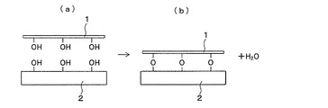
以上のような紫外線照射あるいはプラズマ照射により、空気中の酸素及び照射により酸素から発生したオゾンが紫外線あるいはプラズマと作用して活性酸素が発生する。この活性酸素が、フィルム1の表面を改質する。その結果、フィルム1は、図1のように水酸基を有するようになり接合に適した表面状態になる。
By the ultraviolet irradiation or plasma irradiation as described above, oxygen in the air and ozone generated from the oxygen by irradiation act on the ultraviolet light or plasma to generate active oxygen. This active oxygen modifies the surface of the
なお、図1に示すように、フィルム1と同様に、ガラス2表面にも紫外線あるいはプラズマを照射し、表面改質を行ってもよいし、フィルム1またはガラス2の接合する面のいずれか一方だけに照射してもよい。さらに、図4に示すように、フィルム1同士、ガラス2同士を接合する場合も同様である。
As shown in FIG. 1, similarly to the
(加熱・加圧工程)
その後、表面が改質された、ガラス、樹脂、水晶のいずれかで形成された2つの部材の表面同士を密着させた後に、図2に示すように、これを真空状態にて平面板からなる加圧部材4、5間に配置する。加圧部材としては、面精度が高い金属平面板あるいは面精度が高く弾性を有する部材を選択することができる。
(Heating / pressurizing process)
Thereafter, after the surfaces of two members formed of glass, resin, or quartz whose surfaces are modified are brought into close contact with each other, as shown in FIG. 2, this is made of a flat plate in a vacuum state. Arranged between the
表面処理を行った面同士を接触させ、真空中にて加圧部材間に配置し、加熱及び加圧処理を行う。このとき、加熱温度は50℃から150℃程度の範囲が有効で、最も望ましい温度は80℃程度である。加圧力は1〜10MPaの範囲が有効で、最も望ましい加圧力は約2MPaである。加熱及び加圧処理する処理時間は30秒〜300秒の範囲が有効で、最も望ましい処理時間は100秒程度である。 The surfaces subjected to the surface treatment are brought into contact with each other and placed between the pressure members in a vacuum to perform heating and pressure treatment. At this time, the heating temperature is effectively in the range of about 50 ° C. to 150 ° C., and the most desirable temperature is about 80 ° C. The applied pressure is effectively in the range of 1 to 10 MPa, and the most desirable applied pressure is about 2 MPa. The treatment time for heating and pressurizing is effective in the range of 30 seconds to 300 seconds, and the most desirable treatment time is about 100 seconds.
この加熱および加圧処理によって、図3に示すように、2つの部材の表面は、水が脱離して表面の酸素を介した共有結合により接合される。または、図5に示すように、水酸基同士の水素結合により接合されるか、共有結合および水素結合が混在した状態で接合される。つまり、2つの部材の表面は、接着剤による接着層あるいは接着膜なしで直接的に接合されるのである。 By this heating and pressurizing treatment, as shown in FIG. 3, the surfaces of the two members are bonded by covalent bonding via oxygen on the surfaces as water is desorbed. Alternatively, as illustrated in FIG. 5, bonding is performed by hydrogen bonding between hydroxyl groups, or bonding is performed in a state where a covalent bond and a hydrogen bond are mixed. That is, the surfaces of the two members are directly joined without an adhesive layer or adhesive film made of an adhesive.
(その他)
本発明の方法は、ポリカーボネイトのフィルムとガラスだけではなく、フィルム同士、ガラス同士、あるいは異なる種類のフィルムとの接合にも採用することが可能である。
接合する部材の組み合わせの他の好適例としては、次のものがある。
(a)樹脂フィルムとガラス基板の接合
(b)樹脂フィルムと水晶基板の接合
樹脂フィルムとガラス基板の接合は、フィルムの光学素子の板厚を調整する場合に適用される。例えば、フィルム単体では0.05mm程度であるが、0.5mmのガラス基板を接合すれば0.55mmとなり、剛性も得られる。光学素子は、位相差板や偏光板である。また液晶パネルや、パネルとブラックライトの接合部材、プロジェクタの光学系、携帯電話の液晶パネル、有機ELパネル、太陽電池パネル等に用いられる。
(Other)
The method of the present invention can be employed not only for polycarbonate film and glass but also for bonding films, glasses, or different types of films.
Other suitable examples of the combination of members to be joined include the following.
(A) Bonding of Resin Film and Glass Substrate (b) Bonding of Resin Film and Quartz Substrate Bonding of the resin film and the glass substrate is applied when adjusting the thickness of the optical element of the film. For example, the film itself is about 0.05 mm, but if a 0.5 mm glass substrate is bonded, it becomes 0.55 mm, and rigidity is also obtained. The optical element is a retardation plate or a polarizing plate. It is also used for liquid crystal panels, panel / black light joining members, projector optical systems, mobile phone liquid crystal panels, organic EL panels, solar cell panels, and the like.
また、接合するガラス基板が回折格子である場合、位相差フィルムと接合することにより偏光機能と回折機能を併せ持つ複合光学素子の作製が可能となる。 When the glass substrate to be bonded is a diffraction grating, it is possible to manufacture a composite optical element having both a polarizing function and a diffractive function by bonding to a retardation film.
樹脂の位相差フィルムと水晶基板の接合は、水晶基板が位相差板であれば、樹脂の位相差フィルムの接合と同様に積層による位相差板の広帯域化が可能となる。 If the quartz substrate is a retardation plate, the resin retardation film and the quartz substrate can be bonded to each other in the same manner as the resin retardation film.
水晶基板同士の接合の場合、BD波長のレーザ光への耐光性が高い位相差板の作製が可能となる。 In the case of bonding between quartz substrates, a retardation plate having high light resistance to laser light having a BD wavelength can be produced.
つまり、樹脂の位相差フィルムを用いた位相差板や水晶の位相差板を接着剤や粘着材で貼り合せた位相差板のように、有機材料を部材に用いた位相差板は、BD波長のレーザ光の照射により有機材料部分の劣化が生じる懸念があるが、本発明の製造方法によれば、BD波長のレーザ光の照射による劣化の懸念がない水晶位相差板の作製が可能となる。 In other words, a retardation plate using an organic material as a member, such as a retardation plate using a resin retardation film, or a retardation plate obtained by bonding a quartz retardation plate with an adhesive or an adhesive, is a BD wavelength. Although there is a concern that the organic material portion may be deteriorated by the irradiation of the laser beam, according to the manufacturing method of the present invention, it is possible to manufacture a quartz phase difference plate that is not deteriorated by the irradiation of the laser beam having the BD wavelength. .
(本発明の効果)
本発明は、2つの部材を、接着剤、接合膜等を用いることなく、透過率、耐湿性を維持したまま接合することが可能となる光学素子の製造方法及びその方法を用いて製造した光学素子を提供することができる。そのため、第1の部材と第2の部材の接合部は、外観上、接着剤や粘着材を用いた場合に見られる接着層がなく、歪みなどが生じていないという特徴がある。
(Effect of the present invention)
The present invention provides a method for manufacturing an optical element that can bond two members while maintaining transmittance and moisture resistance without using an adhesive, a bonding film, and the like, and an optical device manufactured using the method. An element can be provided. For this reason, the joint between the first member and the second member is characterized in that there is no adhesive layer seen when an adhesive or a pressure-sensitive adhesive is used and no distortion occurs.
また、複数の工程を順に進める従来の貼り合わせ方法に比べ、加熱および加圧を真空下で同時に行っているので、部材間に含まれる気泡の混入が低減でき、密着力は数倍向上し、部材同士の高精度な位置合わせを行うことができる。 In addition, compared to the conventional bonding method in which a plurality of steps are sequentially performed, since heating and pressurization are simultaneously performed under vacuum, mixing of bubbles contained between members can be reduced, and the adhesion is improved several times. High-precision alignment between members can be performed.
1、1a、1b:フィルム
2、2a、2b:ガラス
3:接合体(光学素子)
4、5:加圧部材(平面板)
1, 1a, 1b:
4, 5: Pressurizing member (flat plate)
Claims (5)
両部材の接合面の少なくとも一方に紫外線またはプラズマを照射して表面改質し、
前記照射後、両部材の前記接合面同士を接触させ、
両部材を真空状態の中に配置し、同時に、その接合面を加熱および加圧することを特徴とする部材の接合方法。 A method of joining a first member and a second member made of resin, glass or crystal,
Irradiate at least one of the joint surfaces of both members with ultraviolet rays or plasma to modify the surface,
After the irradiation, the joining surfaces of both members are brought into contact with each other,
A method for joining members, characterized in that both members are placed in a vacuum state, and at the same time, the joining surfaces are heated and pressurized.
Priority Applications (1)
| Application Number | Priority Date | Filing Date | Title |
|---|---|---|---|
| JP2016067735A JP2017177519A (en) | 2016-03-30 | 2016-03-30 | Method for joining member and optical element produced by the method |
Applications Claiming Priority (1)
| Application Number | Priority Date | Filing Date | Title |
|---|---|---|---|
| JP2016067735A JP2017177519A (en) | 2016-03-30 | 2016-03-30 | Method for joining member and optical element produced by the method |
Publications (1)
| Publication Number | Publication Date |
|---|---|
| JP2017177519A true JP2017177519A (en) | 2017-10-05 |
Family
ID=60009005
Family Applications (1)
| Application Number | Title | Priority Date | Filing Date |
|---|---|---|---|
| JP2016067735A Pending JP2017177519A (en) | 2016-03-30 | 2016-03-30 | Method for joining member and optical element produced by the method |
Country Status (1)
| Country | Link |
|---|---|
| JP (1) | JP2017177519A (en) |
Cited By (9)
| Publication number | Priority date | Publication date | Assignee | Title |
|---|---|---|---|---|
| CN108520854A (en) * | 2018-04-25 | 2018-09-11 | 哈尔滨工业大学 | A method of the glass and other materials placed using UV activation bonding superposing type |
| WO2019188010A1 (en) * | 2018-03-30 | 2019-10-03 | ソニー株式会社 | Optical element, polarization conversion element, image display device, and method for manufacturing optical element |
| JP2020116891A (en) * | 2019-01-25 | 2020-08-06 | 株式会社電子技研 | Bonding structure and bonding method |
| JP2021518583A (en) * | 2018-03-20 | 2021-08-02 | インヴェンサス ボンディング テクノロジーズ インコーポレイテッド | Directly coupled laminates for improved mapping in optical devices |
| JPWO2021260813A1 (en) * | 2020-06-24 | 2021-12-30 | ||
| US11543574B2 (en) | 2019-05-09 | 2023-01-03 | The Japan Steel Works, Ltd. | Wave plate, method for manufacturing wave plate, and optical apparatus |
| US11715730B2 (en) | 2017-03-16 | 2023-08-01 | Adeia Semiconductor Technologies Llc | Direct-bonded LED arrays including optical elements configured to transmit optical signals from LED elements |
| US11762200B2 (en) | 2019-12-17 | 2023-09-19 | Adeia Semiconductor Bonding Technologies Inc. | Bonded optical devices |
| US11860415B2 (en) | 2018-02-26 | 2024-01-02 | Adeia Semiconductor Bonding Technologies Inc. | Integrated optical waveguides, direct-bonded waveguide interface joints, optical routing and interconnects |
Citations (4)
| Publication number | Priority date | Publication date | Assignee | Title |
|---|---|---|---|---|
| JPS60197740A (en) * | 1984-03-21 | 1985-10-07 | Idemitsu Petrochem Co Ltd | Preparation of laminate |
| JP2002234126A (en) * | 2001-02-09 | 2002-08-20 | Amt Kenkyusho:Kk | Polyimide film laminate |
| JP2012076298A (en) * | 2010-09-30 | 2012-04-19 | Topcon Corp | Production method of optical element and optical element produced by the same |
| JP2016030396A (en) * | 2014-07-29 | 2016-03-07 | 三菱電機株式会社 | Laminate device and laminate method |
-
2016
- 2016-03-30 JP JP2016067735A patent/JP2017177519A/en active Pending
Patent Citations (4)
| Publication number | Priority date | Publication date | Assignee | Title |
|---|---|---|---|---|
| JPS60197740A (en) * | 1984-03-21 | 1985-10-07 | Idemitsu Petrochem Co Ltd | Preparation of laminate |
| JP2002234126A (en) * | 2001-02-09 | 2002-08-20 | Amt Kenkyusho:Kk | Polyimide film laminate |
| JP2012076298A (en) * | 2010-09-30 | 2012-04-19 | Topcon Corp | Production method of optical element and optical element produced by the same |
| JP2016030396A (en) * | 2014-07-29 | 2016-03-07 | 三菱電機株式会社 | Laminate device and laminate method |
Cited By (16)
| Publication number | Priority date | Publication date | Assignee | Title |
|---|---|---|---|---|
| US11715730B2 (en) | 2017-03-16 | 2023-08-01 | Adeia Semiconductor Technologies Llc | Direct-bonded LED arrays including optical elements configured to transmit optical signals from LED elements |
| US11860415B2 (en) | 2018-02-26 | 2024-01-02 | Adeia Semiconductor Bonding Technologies Inc. | Integrated optical waveguides, direct-bonded waveguide interface joints, optical routing and interconnects |
| JP2021518583A (en) * | 2018-03-20 | 2021-08-02 | インヴェンサス ボンディング テクノロジーズ インコーポレイテッド | Directly coupled laminates for improved mapping in optical devices |
| JP7436376B2 (en) | 2018-03-20 | 2024-02-21 | アデイア セミコンダクター ボンディング テクノロジーズ インコーポレイテッド | Direct bond stacking for improved image clarity in optical devices |
| JP7322873B2 (en) | 2018-03-30 | 2023-08-08 | ソニーグループ株式会社 | Polarization conversion element and image display device |
| WO2019188010A1 (en) * | 2018-03-30 | 2019-10-03 | ソニー株式会社 | Optical element, polarization conversion element, image display device, and method for manufacturing optical element |
| JPWO2019188010A1 (en) * | 2018-03-30 | 2021-05-13 | ソニーグループ株式会社 | Manufacturing method of optical element, polarization conversion element, image display device and optical element |
| CN108520854B (en) * | 2018-04-25 | 2020-03-31 | 哈尔滨工业大学 | Method for activating, bonding and stacking glass and other materials by utilizing ultraviolet light |
| CN108520854A (en) * | 2018-04-25 | 2018-09-11 | 哈尔滨工业大学 | A method of the glass and other materials placed using UV activation bonding superposing type |
| JP2020116891A (en) * | 2019-01-25 | 2020-08-06 | 株式会社電子技研 | Bonding structure and bonding method |
| JP7312946B2 (en) | 2019-01-25 | 2023-07-24 | 株式会社電子技研 | Bonding structure and bonding method |
| US11543574B2 (en) | 2019-05-09 | 2023-01-03 | The Japan Steel Works, Ltd. | Wave plate, method for manufacturing wave plate, and optical apparatus |
| US11762200B2 (en) | 2019-12-17 | 2023-09-19 | Adeia Semiconductor Bonding Technologies Inc. | Bonded optical devices |
| JP7331260B2 (en) | 2020-06-24 | 2023-08-22 | 三菱重工業株式会社 | Joining method |
| WO2021260813A1 (en) * | 2020-06-24 | 2021-12-30 | 三菱重工業株式会社 | Joining method |
| JPWO2021260813A1 (en) * | 2020-06-24 | 2021-12-30 |
Similar Documents
| Publication | Publication Date | Title |
|---|---|---|
| JP2017177519A (en) | Method for joining member and optical element produced by the method | |
| JP5501918B2 (en) | Optical element manufacturing method and optical element produced by the method | |
| US7952802B2 (en) | Optical device provided with polarizing plate | |
| KR101180292B1 (en) | A Method for Producing Polarizer | |
| TW201809747A (en) | Polarizing plate, image display device and method for manufacturing polarizing plate | |
| KR20080042705A (en) | Process for producing a polarizing plate | |
| TWI549830B (en) | The manufacturing method of the layered body | |
| TWI592720B (en) | Method for manufacturing the bonding device and manufacturing device for the bonding device | |
| JP2010286737A (en) | Polarizing plate and manufacturing method of the same | |
| WO2019216068A1 (en) | Polarizing plate and display device | |
| US20130265641A1 (en) | Three-dimensional image display apparatus | |
| JP2009061735A (en) | Method and apparatus for laminating ultraviolet curable waveguide material | |
| JP6770816B2 (en) | Method of joining members and optical elements manufactured by that method | |
| JP2008051998A (en) | Manufacturing method of optical element | |
| JP6567931B2 (en) | Method for producing laminated optical film | |
| CN110609350B (en) | Optical laminate and method for producing same | |
| JP7122168B2 (en) | Laminate with Adhesive Layer, Laminate, Liquid Crystal Layer Laminate, Method for Producing Liquid Crystal Film, and Method for Producing Optical Laminate | |
| KR101134334B1 (en) | Optical device | |
| JP2019215584A (en) | Manufacturing method for optical laminate | |
| CN107450122B (en) | Bonding system and method for manufacturing optical film using same | |
| JP2018004874A (en) | Optical member and manufacturing method therefor | |
| JP2008051995A (en) | Optical element and manufacturing method of optical element | |
| JP2005189397A (en) | Splice method of thin film filters | |
| JPH03127029A (en) | Production of spacer material, sealing material and liquid crystal panel | |
| JP2014134623A (en) | Optical film, image display device and method for manufacturing optical film |
Legal Events
| Date | Code | Title | Description |
|---|---|---|---|
| A621 | Written request for application examination |
Free format text: JAPANESE INTERMEDIATE CODE: A621 Effective date: 20190121 |
|
| A977 | Report on retrieval |
Free format text: JAPANESE INTERMEDIATE CODE: A971007 Effective date: 20191126 |
|
| A131 | Notification of reasons for refusal |
Free format text: JAPANESE INTERMEDIATE CODE: A131 Effective date: 20191128 |
|
| A601 | Written request for extension of time |
Free format text: JAPANESE INTERMEDIATE CODE: A601 Effective date: 20200123 |
|
| A521 | Request for written amendment filed |
Free format text: JAPANESE INTERMEDIATE CODE: A523 Effective date: 20200326 |
|
| A02 | Decision of refusal |
Free format text: JAPANESE INTERMEDIATE CODE: A02 Effective date: 20200603 |