JP5517800B2 - Member for solid-state imaging device and method for manufacturing solid-state imaging device - Google Patents
Member for solid-state imaging device and method for manufacturing solid-state imaging device Download PDFInfo
- Publication number
- JP5517800B2 JP5517800B2 JP2010156927A JP2010156927A JP5517800B2 JP 5517800 B2 JP5517800 B2 JP 5517800B2 JP 2010156927 A JP2010156927 A JP 2010156927A JP 2010156927 A JP2010156927 A JP 2010156927A JP 5517800 B2 JP5517800 B2 JP 5517800B2
- Authority
- JP
- Japan
- Prior art keywords
- substrate
- wiring structure
- conductor
- insulating film
- state imaging
- Prior art date
- Legal status (The legal status is an assumption and is not a legal conclusion. Google has not performed a legal analysis and makes no representation as to the accuracy of the status listed.)
- Active
Links
- 238000003384 imaging method Methods 0.000 title claims description 62
- 238000000034 method Methods 0.000 title claims description 46
- 238000004519 manufacturing process Methods 0.000 title claims description 39
- 239000000758 substrate Substances 0.000 claims description 128
- 239000004020 conductor Substances 0.000 claims description 61
- 238000006243 chemical reaction Methods 0.000 claims description 37
- 230000002093 peripheral effect Effects 0.000 claims description 32
- 229910052802 copper Inorganic materials 0.000 claims description 24
- 239000010949 copper Substances 0.000 claims description 24
- 229910052751 metal Inorganic materials 0.000 claims description 23
- 239000002184 metal Substances 0.000 claims description 23
- RYGMFSIKBFXOCR-UHFFFAOYSA-N Copper Chemical compound [Cu] RYGMFSIKBFXOCR-UHFFFAOYSA-N 0.000 claims description 20
- 230000003321 amplification Effects 0.000 claims description 13
- 238000005304 joining Methods 0.000 claims description 13
- 238000003199 nucleic acid amplification method Methods 0.000 claims description 13
- 239000011261 inert gas Substances 0.000 claims description 2
- 230000001678 irradiating effect Effects 0.000 claims 1
- 239000010410 layer Substances 0.000 description 109
- 239000011229 interlayer Substances 0.000 description 70
- 239000004065 semiconductor Substances 0.000 description 54
- 230000004888 barrier function Effects 0.000 description 17
- 229910052782 aluminium Inorganic materials 0.000 description 11
- XAGFODPZIPBFFR-UHFFFAOYSA-N aluminium Chemical compound [Al] XAGFODPZIPBFFR-UHFFFAOYSA-N 0.000 description 11
- 238000002955 isolation Methods 0.000 description 7
- VYPSYNLAJGMNEJ-UHFFFAOYSA-N Silicium dioxide Chemical compound O=[Si]=O VYPSYNLAJGMNEJ-UHFFFAOYSA-N 0.000 description 6
- 229910052814 silicon oxide Inorganic materials 0.000 description 6
- 229910052581 Si3N4 Inorganic materials 0.000 description 5
- HQVNEWCFYHHQES-UHFFFAOYSA-N silicon nitride Chemical compound N12[Si]34N5[Si]62N3[Si]51N64 HQVNEWCFYHHQES-UHFFFAOYSA-N 0.000 description 5
- 230000004048 modification Effects 0.000 description 4
- 238000012986 modification Methods 0.000 description 4
- 238000000059 patterning Methods 0.000 description 4
- 239000011347 resin Substances 0.000 description 4
- 229920005989 resin Polymers 0.000 description 4
- XUIMIQQOPSSXEZ-UHFFFAOYSA-N Silicon Chemical compound [Si] XUIMIQQOPSSXEZ-UHFFFAOYSA-N 0.000 description 3
- 230000015572 biosynthetic process Effects 0.000 description 3
- 238000010586 diagram Methods 0.000 description 3
- 238000001312 dry etching Methods 0.000 description 3
- 238000005530 etching Methods 0.000 description 3
- 238000000206 photolithography Methods 0.000 description 3
- 229910052710 silicon Inorganic materials 0.000 description 3
- 239000010703 silicon Substances 0.000 description 3
- IJGRMHOSHXDMSA-UHFFFAOYSA-N Atomic nitrogen Chemical compound N#N IJGRMHOSHXDMSA-UHFFFAOYSA-N 0.000 description 2
- 238000000151 deposition Methods 0.000 description 2
- 239000012212 insulator Substances 0.000 description 2
- 239000000463 material Substances 0.000 description 2
- 229910021420 polycrystalline silicon Inorganic materials 0.000 description 2
- 229920005591 polysilicon Polymers 0.000 description 2
- 230000035945 sensitivity Effects 0.000 description 2
- 239000000126 substance Substances 0.000 description 2
- WFKWXMTUELFFGS-UHFFFAOYSA-N tungsten Chemical compound [W] WFKWXMTUELFFGS-UHFFFAOYSA-N 0.000 description 2
- 229910052721 tungsten Inorganic materials 0.000 description 2
- 239000010937 tungsten Substances 0.000 description 2
- 238000001039 wet etching Methods 0.000 description 2
- RTAQQCXQSZGOHL-UHFFFAOYSA-N Titanium Chemical compound [Ti] RTAQQCXQSZGOHL-UHFFFAOYSA-N 0.000 description 1
- 230000004913 activation Effects 0.000 description 1
- QVGXLLKOCUKJST-UHFFFAOYSA-N atomic oxygen Chemical compound [O] QVGXLLKOCUKJST-UHFFFAOYSA-N 0.000 description 1
- 238000009792 diffusion process Methods 0.000 description 1
- 230000009977 dual effect Effects 0.000 description 1
- 239000007789 gas Substances 0.000 description 1
- 238000010438 heat treatment Methods 0.000 description 1
- 238000009413 insulation Methods 0.000 description 1
- 229910052757 nitrogen Inorganic materials 0.000 description 1
- 239000001301 oxygen Substances 0.000 description 1
- 229910052760 oxygen Inorganic materials 0.000 description 1
- 229920002120 photoresistant polymer Polymers 0.000 description 1
- 238000005498 polishing Methods 0.000 description 1
- 229910052715 tantalum Inorganic materials 0.000 description 1
- GUVRBAGPIYLISA-UHFFFAOYSA-N tantalum atom Chemical compound [Ta] GUVRBAGPIYLISA-UHFFFAOYSA-N 0.000 description 1
- 239000010936 titanium Substances 0.000 description 1
- 229910052719 titanium Inorganic materials 0.000 description 1
Images


Classifications
-
- H—ELECTRICITY
- H01—ELECTRIC ELEMENTS
- H01L—SEMICONDUCTOR DEVICES NOT COVERED BY CLASS H10
- H01L27/00—Devices consisting of a plurality of semiconductor or other solid-state components formed in or on a common substrate
- H01L27/14—Devices consisting of a plurality of semiconductor or other solid-state components formed in or on a common substrate including semiconductor components sensitive to infrared radiation, light, electromagnetic radiation of shorter wavelength or corpuscular radiation and specially adapted either for the conversion of the energy of such radiation into electrical energy or for the control of electrical energy by such radiation
- H01L27/144—Devices controlled by radiation
- H01L27/146—Imager structures
- H01L27/14683—Processes or apparatus peculiar to the manufacture or treatment of these devices or parts thereof
- H01L27/1469—Assemblies, i.e. hybrid integration
-
- H—ELECTRICITY
- H01—ELECTRIC ELEMENTS
- H01L—SEMICONDUCTOR DEVICES NOT COVERED BY CLASS H10
- H01L27/00—Devices consisting of a plurality of semiconductor or other solid-state components formed in or on a common substrate
- H01L27/14—Devices consisting of a plurality of semiconductor or other solid-state components formed in or on a common substrate including semiconductor components sensitive to infrared radiation, light, electromagnetic radiation of shorter wavelength or corpuscular radiation and specially adapted either for the conversion of the energy of such radiation into electrical energy or for the control of electrical energy by such radiation
- H01L27/144—Devices controlled by radiation
- H01L27/146—Imager structures
- H01L27/14601—Structural or functional details thereof
- H01L27/14634—Assemblies, i.e. Hybrid structures
-
- H—ELECTRICITY
- H01—ELECTRIC ELEMENTS
- H01L—SEMICONDUCTOR DEVICES NOT COVERED BY CLASS H10
- H01L27/00—Devices consisting of a plurality of semiconductor or other solid-state components formed in or on a common substrate
- H01L27/14—Devices consisting of a plurality of semiconductor or other solid-state components formed in or on a common substrate including semiconductor components sensitive to infrared radiation, light, electromagnetic radiation of shorter wavelength or corpuscular radiation and specially adapted either for the conversion of the energy of such radiation into electrical energy or for the control of electrical energy by such radiation
- H01L27/144—Devices controlled by radiation
- H01L27/146—Imager structures
- H01L27/14601—Structural or functional details thereof
- H01L27/14636—Interconnect structures
-
- H—ELECTRICITY
- H01—ELECTRIC ELEMENTS
- H01L—SEMICONDUCTOR DEVICES NOT COVERED BY CLASS H10
- H01L27/00—Devices consisting of a plurality of semiconductor or other solid-state components formed in or on a common substrate
- H01L27/14—Devices consisting of a plurality of semiconductor or other solid-state components formed in or on a common substrate including semiconductor components sensitive to infrared radiation, light, electromagnetic radiation of shorter wavelength or corpuscular radiation and specially adapted either for the conversion of the energy of such radiation into electrical energy or for the control of electrical energy by such radiation
- H01L27/144—Devices controlled by radiation
- H01L27/146—Imager structures
- H01L27/14601—Structural or functional details thereof
- H01L27/1464—Back illuminated imager structures
-
- H—ELECTRICITY
- H01—ELECTRIC ELEMENTS
- H01L—SEMICONDUCTOR DEVICES NOT COVERED BY CLASS H10
- H01L27/00—Devices consisting of a plurality of semiconductor or other solid-state components formed in or on a common substrate
- H01L27/14—Devices consisting of a plurality of semiconductor or other solid-state components formed in or on a common substrate including semiconductor components sensitive to infrared radiation, light, electromagnetic radiation of shorter wavelength or corpuscular radiation and specially adapted either for the conversion of the energy of such radiation into electrical energy or for the control of electrical energy by such radiation
- H01L27/144—Devices controlled by radiation
- H01L27/146—Imager structures
- H01L27/14683—Processes or apparatus peculiar to the manufacture or treatment of these devices or parts thereof
- H01L27/14687—Wafer level processing
-
- H—ELECTRICITY
- H01—ELECTRIC ELEMENTS
- H01L—SEMICONDUCTOR DEVICES NOT COVERED BY CLASS H10
- H01L27/00—Devices consisting of a plurality of semiconductor or other solid-state components formed in or on a common substrate
- H01L27/14—Devices consisting of a plurality of semiconductor or other solid-state components formed in or on a common substrate including semiconductor components sensitive to infrared radiation, light, electromagnetic radiation of shorter wavelength or corpuscular radiation and specially adapted either for the conversion of the energy of such radiation into electrical energy or for the control of electrical energy by such radiation
- H01L27/144—Devices controlled by radiation
- H01L27/146—Imager structures
- H01L27/14683—Processes or apparatus peculiar to the manufacture or treatment of these devices or parts thereof
- H01L27/14689—MOS based technologies
-
- H—ELECTRICITY
- H01—ELECTRIC ELEMENTS
- H01L—SEMICONDUCTOR DEVICES NOT COVERED BY CLASS H10
- H01L31/00—Semiconductor devices sensitive to infrared radiation, light, electromagnetic radiation of shorter wavelength or corpuscular radiation and specially adapted either for the conversion of the energy of such radiation into electrical energy or for the control of electrical energy by such radiation; Processes or apparatus specially adapted for the manufacture or treatment thereof or of parts thereof; Details thereof
- H01L31/04—Semiconductor devices sensitive to infrared radiation, light, electromagnetic radiation of shorter wavelength or corpuscular radiation and specially adapted either for the conversion of the energy of such radiation into electrical energy or for the control of electrical energy by such radiation; Processes or apparatus specially adapted for the manufacture or treatment thereof or of parts thereof; Details thereof adapted as photovoltaic [PV] conversion devices
-
- H—ELECTRICITY
- H01—ELECTRIC ELEMENTS
- H01L—SEMICONDUCTOR DEVICES NOT COVERED BY CLASS H10
- H01L2224/00—Indexing scheme for arrangements for connecting or disconnecting semiconductor or solid-state bodies and methods related thereto as covered by H01L24/00
- H01L2224/01—Means for bonding being attached to, or being formed on, the surface to be connected, e.g. chip-to-package, die-attach, "first-level" interconnects; Manufacturing methods related thereto
- H01L2224/02—Bonding areas; Manufacturing methods related thereto
- H01L2224/04—Structure, shape, material or disposition of the bonding areas prior to the connecting process
- H01L2224/05—Structure, shape, material or disposition of the bonding areas prior to the connecting process of an individual bonding area
- H01L2224/0554—External layer
- H01L2224/05599—Material
- H01L2224/056—Material with a principal constituent of the material being a metal or a metalloid, e.g. boron [B], silicon [Si], germanium [Ge], arsenic [As], antimony [Sb], tellurium [Te] and polonium [Po], and alloys thereof
- H01L2224/05638—Material with a principal constituent of the material being a metal or a metalloid, e.g. boron [B], silicon [Si], germanium [Ge], arsenic [As], antimony [Sb], tellurium [Te] and polonium [Po], and alloys thereof the principal constituent melting at a temperature of greater than or equal to 950°C and less than 1550°C
- H01L2224/05655—Nickel [Ni] as principal constituent
-
- H—ELECTRICITY
- H01—ELECTRIC ELEMENTS
- H01L—SEMICONDUCTOR DEVICES NOT COVERED BY CLASS H10
- H01L2224/00—Indexing scheme for arrangements for connecting or disconnecting semiconductor or solid-state bodies and methods related thereto as covered by H01L24/00
- H01L2224/01—Means for bonding being attached to, or being formed on, the surface to be connected, e.g. chip-to-package, die-attach, "first-level" interconnects; Manufacturing methods related thereto
- H01L2224/02—Bonding areas; Manufacturing methods related thereto
- H01L2224/07—Structure, shape, material or disposition of the bonding areas after the connecting process
- H01L2224/08—Structure, shape, material or disposition of the bonding areas after the connecting process of an individual bonding area
- H01L2224/081—Disposition
- H01L2224/0812—Disposition the bonding area connecting directly to another bonding area, i.e. connectorless bonding, e.g. bumpless bonding
- H01L2224/08135—Disposition the bonding area connecting directly to another bonding area, i.e. connectorless bonding, e.g. bumpless bonding the bonding area connecting between different semiconductor or solid-state bodies, i.e. chip-to-chip
- H01L2224/08137—Disposition the bonding area connecting directly to another bonding area, i.e. connectorless bonding, e.g. bumpless bonding the bonding area connecting between different semiconductor or solid-state bodies, i.e. chip-to-chip the bodies being arranged next to each other, e.g. on a common substrate
-
- H—ELECTRICITY
- H01—ELECTRIC ELEMENTS
- H01L—SEMICONDUCTOR DEVICES NOT COVERED BY CLASS H10
- H01L2224/00—Indexing scheme for arrangements for connecting or disconnecting semiconductor or solid-state bodies and methods related thereto as covered by H01L24/00
- H01L2224/80—Methods for connecting semiconductor or other solid state bodies using means for bonding being attached to, or being formed on, the surface to be connected
- H01L2224/80001—Methods for connecting semiconductor or other solid state bodies using means for bonding being attached to, or being formed on, the surface to be connected by connecting a bonding area directly to another bonding area, i.e. connectorless bonding, e.g. bumpless bonding
- H01L2224/80009—Pre-treatment of the bonding area
- H01L2224/8003—Reshaping the bonding area in the bonding apparatus, e.g. flattening the bonding area
- H01L2224/80035—Reshaping the bonding area in the bonding apparatus, e.g. flattening the bonding area by heating means
-
- H—ELECTRICITY
- H01—ELECTRIC ELEMENTS
- H01L—SEMICONDUCTOR DEVICES NOT COVERED BY CLASS H10
- H01L2224/00—Indexing scheme for arrangements for connecting or disconnecting semiconductor or solid-state bodies and methods related thereto as covered by H01L24/00
- H01L2224/80—Methods for connecting semiconductor or other solid state bodies using means for bonding being attached to, or being formed on, the surface to be connected
- H01L2224/80001—Methods for connecting semiconductor or other solid state bodies using means for bonding being attached to, or being formed on, the surface to be connected by connecting a bonding area directly to another bonding area, i.e. connectorless bonding, e.g. bumpless bonding
- H01L2224/8034—Bonding interfaces of the bonding area
- H01L2224/80345—Shape, e.g. interlocking features
-
- H—ELECTRICITY
- H01—ELECTRIC ELEMENTS
- H01L—SEMICONDUCTOR DEVICES NOT COVERED BY CLASS H10
- H01L2224/00—Indexing scheme for arrangements for connecting or disconnecting semiconductor or solid-state bodies and methods related thereto as covered by H01L24/00
- H01L2224/80—Methods for connecting semiconductor or other solid state bodies using means for bonding being attached to, or being formed on, the surface to be connected
- H01L2224/80001—Methods for connecting semiconductor or other solid state bodies using means for bonding being attached to, or being formed on, the surface to be connected by connecting a bonding area directly to another bonding area, i.e. connectorless bonding, e.g. bumpless bonding
- H01L2224/808—Bonding techniques
- H01L2224/80894—Direct bonding, i.e. joining surfaces by means of intermolecular attracting interactions at their interfaces, e.g. covalent bonds, van der Waals forces
- H01L2224/80895—Direct bonding, i.e. joining surfaces by means of intermolecular attracting interactions at their interfaces, e.g. covalent bonds, van der Waals forces between electrically conductive surfaces, e.g. copper-copper direct bonding, surface activated bonding
-
- H—ELECTRICITY
- H01—ELECTRIC ELEMENTS
- H01L—SEMICONDUCTOR DEVICES NOT COVERED BY CLASS H10
- H01L2224/00—Indexing scheme for arrangements for connecting or disconnecting semiconductor or solid-state bodies and methods related thereto as covered by H01L24/00
- H01L2224/80—Methods for connecting semiconductor or other solid state bodies using means for bonding being attached to, or being formed on, the surface to be connected
- H01L2224/80001—Methods for connecting semiconductor or other solid state bodies using means for bonding being attached to, or being formed on, the surface to be connected by connecting a bonding area directly to another bonding area, i.e. connectorless bonding, e.g. bumpless bonding
- H01L2224/808—Bonding techniques
- H01L2224/80894—Direct bonding, i.e. joining surfaces by means of intermolecular attracting interactions at their interfaces, e.g. covalent bonds, van der Waals forces
- H01L2224/80896—Direct bonding, i.e. joining surfaces by means of intermolecular attracting interactions at their interfaces, e.g. covalent bonds, van der Waals forces between electrically insulating surfaces, e.g. oxide or nitride layers
-
- H—ELECTRICITY
- H01—ELECTRIC ELEMENTS
- H01L—SEMICONDUCTOR DEVICES NOT COVERED BY CLASS H10
- H01L2224/00—Indexing scheme for arrangements for connecting or disconnecting semiconductor or solid-state bodies and methods related thereto as covered by H01L24/00
- H01L2224/80—Methods for connecting semiconductor or other solid state bodies using means for bonding being attached to, or being formed on, the surface to be connected
- H01L2224/80001—Methods for connecting semiconductor or other solid state bodies using means for bonding being attached to, or being formed on, the surface to be connected by connecting a bonding area directly to another bonding area, i.e. connectorless bonding, e.g. bumpless bonding
- H01L2224/80909—Post-treatment of the bonding area
- H01L2224/8093—Reshaping
- H01L2224/80935—Reshaping by heating means, e.g. reflowing
-
- H—ELECTRICITY
- H01—ELECTRIC ELEMENTS
- H01L—SEMICONDUCTOR DEVICES NOT COVERED BY CLASS H10
- H01L2224/00—Indexing scheme for arrangements for connecting or disconnecting semiconductor or solid-state bodies and methods related thereto as covered by H01L24/00
- H01L2224/80—Methods for connecting semiconductor or other solid state bodies using means for bonding being attached to, or being formed on, the surface to be connected
- H01L2224/80001—Methods for connecting semiconductor or other solid state bodies using means for bonding being attached to, or being formed on, the surface to be connected by connecting a bonding area directly to another bonding area, i.e. connectorless bonding, e.g. bumpless bonding
- H01L2224/80986—Specific sequence of steps, e.g. repetition of manufacturing steps, time sequence
-
- Y—GENERAL TAGGING OF NEW TECHNOLOGICAL DEVELOPMENTS; GENERAL TAGGING OF CROSS-SECTIONAL TECHNOLOGIES SPANNING OVER SEVERAL SECTIONS OF THE IPC; TECHNICAL SUBJECTS COVERED BY FORMER USPC CROSS-REFERENCE ART COLLECTIONS [XRACs] AND DIGESTS
- Y02—TECHNOLOGIES OR APPLICATIONS FOR MITIGATION OR ADAPTATION AGAINST CLIMATE CHANGE
- Y02E—REDUCTION OF GREENHOUSE GAS [GHG] EMISSIONS, RELATED TO ENERGY GENERATION, TRANSMISSION OR DISTRIBUTION
- Y02E10/00—Energy generation through renewable energy sources
- Y02E10/50—Photovoltaic [PV] energy
Description
本発明は、固体撮像装置の接合部に関する発明である。 The present invention relates to a joint portion of a solid-state imaging device.
デジタルスチルカメラやカムコーダなどに用いられるCCD型や増幅型の固体撮像装置においては、高精細の画像を得るためにその画素の微細化が求められている。しかし、画素を微細にすればするほど、画素に含まれる光を検出するための光電変換素子の受光面積が小さくなり、感度が低下してしまう。 In a CCD-type or amplification-type solid-state imaging device used for a digital still camera, a camcorder, and the like, the pixels are required to be miniaturized in order to obtain a high-definition image. However, the finer the pixel, the smaller the light receiving area of the photoelectric conversion element for detecting the light contained in the pixel, resulting in lower sensitivity.
特許文献1には、増幅型の固体撮像装置であるCMOS型の固体撮像装置において、光電変換素子の受光面積を確保するため、光電変換素子と転送トランジスタを配した第1基板と、他の回路を配した第2基板とを接合した固体撮像装置が開示されている。また、特許文献1の固体撮像装置においては、第1基板と第2基板との接合の際に、銅のボンディングパッドを利用し、第2基板の銅ボンディングパッドの周りの絶縁膜をリセスさせることが記載されている。
In
しかしながら、特許文献1に記載の接合の方法では、銅のボンディングパッドの熱膨張係数と絶縁膜の熱膨張係数の関係が検討されておらず、接合後の接合面に隙間が生じる可能性がある。また、凸部となっている銅のボンディングパッドの周りに隙間が生じてしまう場合には、ボンディングパッドである銅が拡散してしまう可能性がある。固体撮像装置において銅が拡散してしまうと、白傷などの問題を生じてしまう。
However, in the bonding method described in
よって、本発明においては、隙間のない接合面を有する固体撮像装置用の基板および製造方法を提供する。 Therefore, the present invention provides a substrate and a manufacturing method for a solid-state imaging device having a joint surface without a gap.
本発明の固体撮像装置の製造方法は、光電変換素子が主面に配された第1基板と、前記第1基板の主面の上に配され、第1導電体からなる配線構造である第1接合部を有し、前記第1導電体が構成する上面を有する第1配線構造とを準備する工程と、前記光電変換素子の電荷に基づく信号を読み出すための読み出し回路および制御回路を含む周辺回路の一部が主面に配された第2基板と、前記第2基板の主面の上に配され、第2導電体からなる配線構造である第2接合部を有し、前記第2導電体が構成する上面を有する第2配線構造とを準備する工程と、前記第1基板と、前記第1配線構造と、前記第2配線構造と、前記第2基板とがこの順に配置されるように接合する工程と、を有する固体撮像装置の製造方法において、前記接合する工程において、前記第1接合部の前記第1導電体と前記第2接合部の前記第2導電体とを金属接合させ、前記第1基板と第1配線構造とを準備する工程、および前記第2基板と前記第2配線構造とを準備する工程において、下記条件(a)および(b)の少なくとも1つを満たす。(a)前記第1基板と、第1配線構造とを準備する工程において、前記第1配線構造の上面は前記第1導電体が底面を構成する凹部を有する。(b)前記第2基板と、前記第2配線構造とを準備する工程において、前記第2配線構造の上面は前記第2導電体が底面を構成する凹部を有する。 The method for manufacturing a solid-state imaging device according to the present invention is a first substrate having a photoelectric conversion element disposed on a main surface and a wiring structure including a first conductor disposed on the main surface of the first substrate. A step of preparing a first wiring structure having one junction and having an upper surface formed by the first conductor, and a peripheral including a read circuit and a control circuit for reading a signal based on the charge of the photoelectric conversion element A second substrate in which a part of the circuit is disposed on a main surface; and a second bonding portion that is disposed on the main surface of the second substrate and has a wiring structure made of a second conductor. A step of preparing a second wiring structure having an upper surface formed of a conductor, the first substrate, the first wiring structure, the second wiring structure, and the second substrate are arranged in this order. the method of manufacturing a solid-state imaging device having a step of joining to the step of the bonding Oite, wherein said first conductor of the first joint portion and the second conductor of the second joint is a metal joint, a step of preparing a first substrate and a first wiring structure, and the second In the step of preparing the two substrates and the second wiring structure, at least one of the following conditions (a) and (b) is satisfied . (A) In the step of preparing the first substrate and the first wiring structure, the upper surface of the first wiring structure has a recess in which the first conductor constitutes the bottom surface. (B) In the step of preparing the second substrate and the second wiring structure, the upper surface of the second wiring structure has a recess in which the second conductor forms the bottom surface.
また、本発明の固体撮像装置の製造方法は、光電変換素子と、前記光電変換素子の電荷を転送する転送トランジスタとが主面に配された第1基板と、前記第1基板の主面の上に配され、第1絶縁膜と第1導電体からなる配線構造である第1接合部を含み、前記第1導電体が構成する上面を有する第1配線構造と、前記光電変換素子の電荷に基づく信号を読み出すための読み出し回路および制御回路を含む周辺回路部の一部が主面に配された第2基板と、前記第2基板の主面の上に配され、第2絶縁膜と第2導電体からなる配線構造である第2接合部を含み、前記第2導電体が構成する上面を有する第2配線構造と、を有し、前記第1基板と、前記第1配線構造と、前記第2配線構造と、前記第2基板とがこの順に配置された固体撮像装置の製造方法において、前記第1絶縁膜および前記第1接合部を前記第1基板の上に形成する工程と、前記第2絶縁膜および前記第2接合部を前記第2基板の上に形成する工程と、前記第1接合部の前記第1導電体と前記第2接合部の前記第2導電体とを金属接合させる工程と、を有し、前記第1絶縁膜および前記第1接合部を前記第1基板の上に形成する工程、および前記第2絶縁膜および前記第2接合部を前記第2基板の上に形成する工程において、下記条件(a)および(b)の少なくとも1つを満たす。(a)前記第1絶縁膜および前記第1接合部を前記第1基板の上に形成する工程において、前記第1基板の主面を基準に前記第1接合部の前記第1導電体の上面が前記第1絶縁膜の上面よりも低い。(b)前記第2絶縁膜および前記第2接合部を前記第2基板の上に形成する工程において、前記第2基板の主面を基準に前記第2接合部の前記第2導電体の上面が前記第2絶縁膜の上面よりも低い。 The solid-state imaging device manufacturing method of the present invention includes a first substrate on which a photoelectric conversion element and a transfer transistor that transfers charges of the photoelectric conversion element are arranged on a main surface, and a main surface of the first substrate. A first wiring structure that includes a first junction portion that is a wiring structure including a first insulating film and a first conductor and has an upper surface that is formed by the first conductor; and a charge of the photoelectric conversion element A peripheral circuit portion including a readout circuit and a control circuit for reading a signal based on the second substrate, a second substrate disposed on the main surface, a second insulating film disposed on the main surface of the second substrate, A second wiring structure including a second bonding portion, which is a wiring structure made of a second conductor, and having an upper surface formed by the second conductor, the first substrate, and the first wiring structure , Manufacturing the solid-state imaging device in which the second wiring structure and the second substrate are arranged in this order. In the method, the step of forming the first insulating film and the first bonding portion on the first substrate, and the step of forming the second insulating film and the second bonding portion on the second substrate; has the steps of causing the metal bonding the second conductor of the second joint portion and the first conductor of the first joint portion, the said first insulating film and the first joint portion first In the step of forming on one substrate and the step of forming the second insulating film and the second bonding portion on the second substrate, at least one of the following conditions (a) and (b) is satisfied. (A) In the step of forming the first insulating film and the first bonding portion on the first substrate, the upper surface of the first conductor of the first bonding portion based on the main surface of the first substrate Is lower than the upper surface of the first insulating film . (B) In the step of forming the second insulating film and the second bonding portion on the second substrate, the upper surface of the second conductor of the second bonding portion based on the main surface of the second substrate. There have lower than the upper surface of the second insulating film.
本発明によって、隙間のない接合面を有する固体撮像装置用の部材および製造方法を提供する。 According to the present invention, there are provided a member and a manufacturing method for a solid-state imaging device having a joint surface without a gap.
本発明の固体撮像装置の製造方法は、光電変換素子が主面に配された第1基板と、第1配線構造とを準備する工程と、周辺回路の一部が主面に配された第2基板と、第2基板の主面の上に配された第2配線構造とを準備する工程を有する。ここで、第1基板、第1配線構造、第2配線構造、第2基板とがこの順に配置されるように接合する工程を有する。そして、少なくとも第1配線構造の上面あるいは第2配線構造の上面のいずれかに凹部が配置され、凹部の底面は導電体が配されている。このような構成によって、接合後の接合面を平面にすることが可能となる。 The method for manufacturing a solid-state imaging device according to the present invention includes a step of preparing a first substrate on which a photoelectric conversion element is arranged on a main surface and a first wiring structure, and a step in which a part of a peripheral circuit is arranged on the main surface. A step of preparing two substrates and a second wiring structure disposed on a main surface of the second substrate. Here, it has the process of joining so that a 1st board | substrate, a 1st wiring structure, a 2nd wiring structure, and a 2nd board | substrate may be arrange | positioned in this order. A recess is disposed at least on either the top surface of the first wiring structure or the top surface of the second wiring structure, and a conductor is disposed on the bottom surface of the recess. With such a configuration, it is possible to make the bonded surface flat after bonding.
以下、本発明について図面を用いて詳細に説明を行う。なお、実施例の説明において、第1基板の主面及び第2基板の主面とはトランジスタが形成される基板表面である。該主面と対向する反対側の面が、第1基板の裏面及び第2基板の裏面である。また、上方向は裏面から主面に向かう方向とし、下方向及び深さ方向は基板の主面から裏面に向かう方向とする。また、ある基準に対して上方向を高さとし、ある基準にたいして下方向を深さとする。 Hereinafter, the present invention will be described in detail with reference to the drawings. In the description of the embodiments, the main surface of the first substrate and the main surface of the second substrate are substrate surfaces on which transistors are formed. The opposite surfaces facing the main surface are the back surface of the first substrate and the back surface of the second substrate. Further, the upward direction is a direction from the back surface to the main surface, and the downward direction and the depth direction are directions from the main surface of the substrate to the back surface. Further, the upper direction is a height with respect to a certain reference, and the lower direction is a depth with respect to a certain reference.
本発明の実施例1について、図1から図6を用いて説明する。まず、図3を用いて実施例1の固体撮像装置の回路を説明する。本実施例では、信号電荷が、例えば電子の場合について説明を行う。図3の固体撮像装置は、複数の光電変換素子が配列した画素部301と、画素部301からの信号を読み出す駆動のための制御回路や読み出した信号を処理する信号処理回路を含む周辺回路を有する周辺回路部302とを有する。
A first embodiment of the present invention will be described with reference to FIGS. First, the circuit of the solid-state imaging device according to the first embodiment will be described with reference to FIG. In this embodiment, the case where the signal charge is, for example, electrons will be described. The solid-state imaging device in FIG. 3 includes a peripheral circuit including a
画素部301は、光電変換素子303と、転送トランジスタ304と、増幅トランジスタ306と、リセットトランジスタ307が複数配置されている。少なくとも1つの光電変換素子303を含む構成を画素とする。本実施例の1つの画素は、光電変換素子303と、転送トランジスタ304と、増幅トランジスタ306と、リセットトランジスタ307を含む。転送トランジスタ304のソースは光電変換素子303と接続しており、転送トランジスタ304のドレイン領域は増幅トランジスタ306のゲート電極と接続している。この増幅トランジスタ306のゲート電極と同一のノードをノード305とする。リセットトランジスタはノード305に接続し、ノード305の電位を任意の電位(例えば、リセット電位)に設定する。ここで、増幅トランジスタ306はソースフォロア回路の一部であり、ノード305の電位に応じた信号を信号線RLに出力する。ノード305はフローティングディフュージョンとも称される場合がある。
In the
周辺回路部302は、画素部301以外の領域を示している。周辺回路部302は、読み出し回路や制御回路を含む周辺回路が配置されている。周辺回路は、画素部301のトランジスタのゲート電極へ制御信号を供給するための制御回路である垂直走査回路VSRを有する。また、周辺回路は、画素部301から出力された信号を保持し、増幅や加算やAD変換などの信号処理を行う読み出し回路RCを有する。また、周辺回路は、読み出し回路RCから信号を順次出力するタイミングを制御する制御回路である水平走査回路HSRを有する。
A
ここで、実施例1の固体撮像装置は2つの部材が張り合わされることによって構成されている。2つの部材とは、第1の基板101を有する第1部材308と第2の基板121を有する第2部材309である。第1基板には画素部301の光電変換素子303と、転送トランジスタ304とが配されており、第2基板には画素部301の増幅トランジスタ306と、リセットトランジスタ307と、周辺回路の少なくとも一部とが配されている。例えば、第2部材309の周辺回路から第1部材308の転送トランジスタ304のゲート電極へ供給される制御信号は、接合部310を介して供給される。接合部310の構成については後述する。第1部材308の光電変換素子303にて生じた信号は、転送トランジスタ304のドレイン領域、即ちノード305に読み出される。ノード305は、第1部材308に配された構成と第2部材309に配された構成とを含む。
Here, the solid-state imaging device according to the first embodiment is configured by bonding two members. The two members are a
このような構成によって、従来の1つの部材(即ち1つの基板)に画素部を全て配置する場合に比べて、光電変換素子303の面積を大きくすることが可能となり感度の向上させることが可能となる。また、従来の1つの部材(即ち1つの基板)に画素部を全て配置する場合に比べて、光電変換素子の面積を同一とするならば、光電変換素子303を多く設けることが可能となり、多画素化が可能となる。また、1つの部材(即ち1つの基板)に画素部を全て配置する場合には、画素部と周辺回路部との作り分けが容易となる。
With such a configuration, the area of the
このような固体撮像装置の具体的な平面レイアウトを、図2の固体撮像装置の平面模式図を用いて説明する。図2(A)は第1部材308、即ち第1基板(101)における平面レイアウトを示し、図2(B)は第2部材309、即ち第2基板(121)の平面レイアウトを示している。
A specific planar layout of such a solid-state imaging device will be described with reference to a schematic plan view of the solid-state imaging device in FIG. 2A shows a planar layout of the
図2(A)において、第1部材308には、複数の光電変換素子が配列した画素部301Aと、パッド313が配されたパッド部312A、とが配されている。画素部301Aには、図3における光電変換素子303と転送トランジスタ304と接合部310、311とが複数配されている。また、パッド313と平面的に同一位置に第2部材309との接続のための接合部314Aが配されている。パッド313には外部端子が接続される。パッド313は固体撮像装置に複数配置されており、光電変換素子で生じた電荷に基づく信号(画像信号)を出力するパッドや、外部から供給される周辺回路を駆動するための電圧などが入力されるパッドが含まれる。
2A, the
次に、図2(B)において、第2部材309には、画素部301Bと周辺回路部302とパッド部312Bとが配されている。画素部301Bには画素回路の一部が配されており、図3における増幅トランジスタ306とリセットトランジスタ307と接合部310と接合部311とが複数配置されている。周辺回路部302には周辺回路の一部が配されており、水平走査回路HSR、垂直走査回路VSR、読み出し回路RCとが配されている。パッド部312Bには、第1部材との接続のための接合部314Bと保護ダイオード回路315とが配されている。
Next, in FIG. 2B, the
そして、図2(A)及び図2(B)に示した平面レイアウトを有する第1部材308と第2部材309とが張り合わされて本実施例の固体撮像装置を構成している。具体的には、画素部301Aと画素部301Bとが重なるように配置される。そして、接合部314Aと接合部314Bとが接合し、第1部材の接合部310、接合部311と、第2部材の接合部310、接合部311とが接合する。なお、図2では、第2部材309の周辺回路部302Bに対応する第1部材308の領域を周辺回路部302Aで示している。周辺回路部302Aには走査回路の一部、即ち周辺回路の一部を配置してもよい。この接合部の構造については、後に詳述する。
Then, the
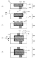
次に、図2及び図3に示した固体撮像装置の断面模式図を、図1を用いて説明する。図1では図2、図3と同一の構成には同一の符号を付し、説明を省略する。 Next, a schematic cross-sectional view of the solid-state imaging device shown in FIGS. 2 and 3 will be described with reference to FIG. In FIG. 1, the same components as those in FIGS. 2 and 3 are denoted by the same reference numerals, and description thereof is omitted.
第1部材308は、第1配線構造149と第1基板101とを有する。第1基板101は例えばシリコン半導体基板であり、主面102と裏面103とを有する。第1基板の主面102にはトランジスタが配置されている。第1配線構造149は、層間絶縁膜104〜106と、ゲート電極や配線を含むゲート電極層107と、複数の配線を含む配線層109、111と、複数のコンタクトあるいはビアを含むコンタクト層108、110とを有する。ここで第1配線構造149に含まれる層間絶縁膜、配線層及びコンタクト層の層数は任意に設定可能である。なお、第1配線構造149の配線層111は、接合部を含む。
The
第1部材308の画素部301において、第1基板101には、光電変換素子を構成するn型半導体領域112と、転送トランジスタのドレインであるn型半導体領域114と、素子分離構造119とが配されている。転送トランジスタはn型半導体領域112とn型半導体領域114と、ゲート電極層107に含まれるゲート電極113とで構成される。ここで、n型半導体領域112で蓄積された電荷は、ゲート電極113によって、n型半導体領域114に転送される。n型半導体領域114に転送された電荷に基づく電位はコンタクト層108のコンタクト、配線層109の配線、コンタクト層110のビア、配線層111の配線を介して、第2部材309へと伝達される。この配線層111の配線は、接合部311を構成する。なお、光電変換素子は更にp型半導体領域を有する埋込みフォトダイオードであってもよく、フォトゲートであってもよく、適宜変更可能である。
In the
画素部301の第1基板101の裏面103側には、平坦化層115、複数のカラーフィルタを含むカラーフィルタ層116、平坦化層117、複数のマイクロレンズを含むマイクロレンズ層118がこの順に配置されている。図1において、複数のカラーフィルタ及び複数のマイクロレンズはそれぞれが1つの光電変換素子に対応して、すなわち画素毎に配置されているが、複数画素に対して1つずつ設けられていてもよい。本実施例の固体撮像装置は、このマイクロレンズ層118側から光が入射し光電変換素子が受光する、所謂、裏面照射型の固体撮像装置である。
On the
第1部材308のパッド部312には、パッド313と、外部端子と接続させるためのパッド313を露出する開口100とが配されている。また、パッド313から入力された電圧を第2部材309に伝達する接合部314Aが配置されている。なお、第1部材308において、第2部材309の周辺回路部302に対応する領域には、図1に示したように任意の回路素子120を設けられていても良い。なお、以下、接合部とは電気的な接続を行う第1部材の導電体と第2部材の導電体とが接合している部分であり、接合前の導電体についても接合部と示すものとする。
The
第2部材309は、第2配線構造150と第2基板121とを有する。第2基板121は例えばシリコン半導体基板であり、主面122と裏面123とを有する。第2基板の主面122にはトランジスタが配置される。第2配線構造150は、層間絶縁膜124〜127と、ゲート電極や配線を含むゲート電極層128と、複数の配線を含む配線層130、132、134と、複数のコンタクトあるいはビアを含むコンタクト層129、131、133とを有する。ここで第2配線構造150に含まれる層間絶縁膜、配線層及びコンタクト層の層数は任意に設定可能である。なお、配線層134は、接合部を含む。
The
第2部材309の画素部301において、第2基板121には、画素回路を構成する増幅トランジスタを構成するウエル135と、増幅トランジスタのソース・ドレイン領域を構成するn型半導体領域138と、素子分離構造136とが配されている。増幅トランジスタは、ウエル135に配され、ゲート電極層128に含まれるゲート電極137と、ソース・ドレイン領域を構成するn型半導体領域138とで構成される。ここで、第1部材308の接合部311と増幅トランジスタのゲート電極137とは、配線層134の配線、コンタクト層133のビア、配線層132の配線、コンタクト層131のビア、配線層130の配線、コンタクト層129のコンタクトとを介して接続される。ここで、図3のノード305は、図1のn型半導体領域114と、配線層109、111、134、132、130の配線と、コンタクト層108、110、133、131、129のコンタクトあるいはビアと、ゲート電極137と、から構成される。画素部301の他の回路(例えば、リセットトランジスタ)は不図示である。
In the
次に、第2部材309の周辺回路部302には、水平走査回路や垂直走査回路等の制御回路や読み出し回路を含む周辺回路の少なくとも一部が配置されている。図1では、周辺回路に含まれる任意の回路におけるn型のトランジスタとp型のトランジスタを示している。ゲート電極層128に含まれるゲート電極140と、n型のソース・ドレイン領域141とからなるn型トランジスタがp型のウエル139に配置されている。そして、ゲート電極層128に含まれるゲート電極143と、p型のソース・ドレイン領域を構成するp型半導体領域144と、を有するp型トランジスタがn型のウエル142に配置されている。
Next, in the
そして、第2部材309のパッド部312には、第1部材308のパッド313からの信号を入力するための保護ダイオード回路315と、第1部材308と接合するための接合部314Bとが配置されている。本実施例の保護ダイオード回路315には、半導体領域から構成される2つのダイオード145、146と、ゲート電極層128からなる2つの抵抗147、148とが含まれている。しかし、保護ダイオード回路315は、一般に使用される保護ダイオード回路が適用可能である。
The
そして、本実施例の固体撮像装置においては、第1基板101の主面102と第2基板121の主面122とが、第1、第2配線構造を介して向かい合う向きに配置されている(対向配置)。つまり、第1基板、第1配線構造、第2配線構造、第2基板の順に配置されている。また、第1配線構造149の上面と、第2配線構造150の上面とが、接合面Xにおいて張り合わされているとも言える。つまり、第1部材308と第2部材309とが接合面Xにて接合されている。接合面Xは、第1配線構造149の上面と第2配線構造150の上面とで構成される。そして、外部と信号のやりとりを行うための固体撮像装置のパッド313が第2部材309の主面122の上部に配置され、第1部材308側に開口100が設けられている。
In the solid-state imaging device according to the present embodiment, the
ここで、第1配線構造149において、配線層109はアルミニウムを主成分とする配線(アルミニウム配線)からなり、配線層111は銅を主成分とする配線(銅配線)からなる。また、第2配線構造150においては、配線層131及び配線層132はアルミニウム配線からなり、配線層134は銅配線からなる。この時、接合面Xにおいて、銅配線からなる配線層111及び配線層134に含まれる接合部311及び接合部314(314A及び314B)が金属接合により接合している。また、パッド部において、外部端子との接続を行うパッド313は、配線層109と同一層、即ち同一高さに配置されており、アルミニウムを主成分とする導電体である。なお、高さとは第1基板101の主面102からの高さである。
Here, in the
次に、本実施例の固体撮像装置の製造方法を、図4〜6を用いて説明する。図4は第1部材308の製造工程を示す断面模式図であり、図5は第2部材309の製造工程を示す断面模式図であり、図6は第1部材308と第2部材309とを接合した後の製造工程を示す断面模式図である。
Next, a method for manufacturing the solid-state imaging device according to the present embodiment will be described with reference to FIGS. 4 is a schematic cross-sectional view showing the manufacturing process of the
図1の第1部材308の製造工程を、図4を用いて説明する。図4においては、後に図1の第1部材308になる構成を308’とし、図1の画素部301、周辺回路部302、パッド部312、周辺回路の一部である回路素子120になる部分を304’、302’、312’、120’としている。
A manufacturing process of the
まず、半導体基板を準備し、半導体基板に素子を形成する。主面402と裏面403を有する厚みD3の半導体基板401を用意する。半導体基板401は例えばシリコン半導体基板である。半導体基板401に、素子分離構造119を形成する。素子分離構造119は、シリコン酸化膜などの絶縁体を含み、例えばLOCOSやSTI構造を有する。そして、半導体基板401に任意の導電型のウエル(不図示)を形成する。その後、光電変換素子やトランジスタを構成するn型半導体領域112、114、及びp型半導体領域(不図示)を形成する。また、転送トランジスタのゲート電極113を含むゲート電極を含むゲート電極層107を形成する。ゲート電極層は例えば、ポリシリコン層の堆積及びパターニングによって形成され、ゲート電極のみではなく配線をも含みうる。ここで、ゲート電極、素子分離及び半導体領域の形成方法については、一般的な半導体プロセスで形成可能であり、詳細な説明は省略する。以上によって、図4(A)の構成が得られる。
First, a semiconductor substrate is prepared, and an element is formed on the semiconductor substrate. A
次に、半導体基板401の主面402上に配線構造を形成する。配線構造は、層間絶縁膜104’、105、106と、コンタクト層108、110と、配線層109、111と、を有する。ここで、層間絶縁膜104’は、後に図1の層間絶縁膜104となる。層間絶縁膜104’はゲート電極層107を覆い、コンタクト層108は層間絶縁膜104’に配され、配線層109は層間絶縁膜104’上に配されている。また、層間絶縁膜105は配線層109を覆い、コンタクト層110は層間絶縁膜105に配され、配線層111は層間絶縁膜105上に配され、層間絶縁膜106は層間絶縁膜105上に配され且つ配線層111の配線が露出するような開口を有する。配線構造の上面は、層間絶縁膜106の上面及び配線層111の上面により形成される。
Next, a wiring structure is formed on the
ここで、層間絶縁膜104’、105、106はシリコン酸化膜である。しかし層間絶縁膜104’、105、106はシリコン窒化膜、あるいは有機樹脂等で形成されてもよい。コンタクト108及びビア110は、例えばタングステンで形成される。配線層109はアルミニウムを主成分とする配線からなり、配線層111は銅を主成分とする配線からなる。配線層111は接合部314A及び311Aを含み、配線層109はパッド313を含む。銅を主成分とする配線層の配線は、シングルダマシン法によって層間絶縁膜に溝を形成しバリアメタルや銅を埋め込むことによって形成することが可能である。アルミニウムを主成分とする配線層の配線は、層間絶縁膜上に成膜されたバリアメタルやアルミニウム膜を、フォトリソグラフィ技術及びエッチング技術によって、パターニングすることによって形成することが可能である。これら配線層、コンタクト層、層間絶縁膜の製造方法については、一般的な半導体プロセスで形成可能であり、詳細な説明は省略する。以上によって、図4(B)の構成が得られる。図4(B)において、符号104’、105、106、108〜111は後に図1における第1配線構造149となる。また、接合部311Aは後に接合部311を構成する。
Here, the
この図4(B)において、後に図1の接合面Xを構成する第1配線構造149の上面は、層間絶縁膜106の上面と配線層111の各配線の上面とによって構成されている。この接合面Xを構成する上面の構造については後に詳述する。
In FIG. 4B, the upper surface of the
次に、図1の第2部材309の製造工程を、図5を用いて説明する。図5においては、後に図1の第2部材309となる構成を309’とし、図1の画素部301、周辺回路部302、パッド部312、保護ダイオード回路315になる部分を304’、302’、312’、315’としている。
Next, the manufacturing process of the
まず、半導体基板を準備し、半導体基板に素子を形成する。主面405と裏面406を有する厚みD4の半導体基板404を用意する。そして、半導体基板404にLOCOSやSTI構造を用いて素子分離構造136を形成する。また、半導体基板404にp型のウエル135、139やn型のウエル142を形成する。その後、トランジスタを構成するソース・ドレイン領域となりうるn型半導体領域138、141、及びp型半導体領域144や、ダイオードを構成する半導体領域を形成する。そして、トランジスタのゲート電極137、140、143及び配線(抵抗)を含むゲート電極層128をポリシリコン層の堆積及びパターニングによって形成する。ここで、ゲート電極、素子分離及び半導体領域の形成方法については、一般的な半導体プロセスで形成可能であり、詳細な説明は省略する。以上によって、図5(A)の構成が得られる。
First, a semiconductor substrate is prepared, and an element is formed on the semiconductor substrate. A
次に、半導体基板404の主面405上に配線構造を形成する。配線構造は、層間絶縁膜124〜127と、コンタクト層129、131、133と、配線層130、132、134とを有する。層間絶縁膜124はゲート電極層128を覆い、コンタクト層129は層間絶縁膜124に配され、配線層130は層間絶縁膜124上に配されている。また、層間絶縁膜125は配線層130を覆い、コンタクト層131は層間絶縁膜125に配され、配線層132は層間絶縁膜125上に配され、層間絶縁膜126は配線層132を覆い層間絶縁膜125上に配される。そして、コンタクト層133は層間絶縁膜126に配され、配線層134は層間絶縁膜126上に配され、層間絶縁膜127は層間絶縁膜126上に配され、且つ配線層134の配線を露出する開口を有する。配線構造の上面は、層間絶縁膜127の上面及び配線層134の上面により形成される。
Next, a wiring structure is formed on the
ここで、層間絶縁膜124〜127はシリコン酸化膜である。層間絶縁膜124〜127はシリコン窒化膜、あるいは有機樹脂等で形成されてもよい。コンタクト129及びビア131、133は、例えばタングステンで形成される。配線層130、132はアルミニウムを主成分とする配線からなり、配線層134は銅を主成分とする配線からなる。配線層134は接合部314B及び311Bを含む。銅を主成分とする配線層の配線は、シングルダマシン法によって層間絶縁膜に溝を形成しバリアメタルや銅を埋め込むことによって形成することが可能である。アルミニウムを主成分とする配線層の配線は、層間絶縁膜上に成膜されたバリアメタルやアルミニウム膜を、フォトリソグラフィ技術及びエッチング技術によって、パターニングすることによって形成することが可能である。これら配線層、コンタクト層、層間絶縁膜の製造方法については、一般的な半導体プロセスで形成可能であり、詳細な説明は省略する。以上によって、図5(B)の構成が得られる。図5(B)において、符号124〜127、129〜134等は後に図1における第2配線構造150となる。また、接合部311Bは後に接合部311を構成する。
Here, the
この図5(B)において、後に図1の接合面Xを構成する第2配線構造の上面は、層間絶縁膜127の上面と配線層134の各配線の上面とによって構成されている。配線層134は接合部となる導電体でもある。つまり、第2配線構造の上面は導電体の上面を含む。この第2配線構造の上面の構造については後に詳述する。
In FIG. 5B, the upper surface of the second wiring structure that will later form the bonding surface X of FIG. 1 is constituted by the upper surface of the
このような図4(B)及び図5(B)に示した第1部材308’と第2部材309’とを、互いの半導体基板の主面402及び主面405とが向かい合うように張り合わせる。つまり、第1部材308’の配線構造の最上面と第2部材309’の配線構造の最上面とが接合される。ここで、接合部311及び接合部209A及び209Bは銅を主成分とする配線から構成されているため、張り合わせの際は銅の金属接合によって行うことが可能である。
The
第1部材308’と第2部材309’とが接合された後に、第1部材308’の半導体基板401の裏面403側を薄膜化する。薄膜化は、CMP(化学的機械研磨)やエッチングによって行うことが可能である。そして、半導体基板401は半導体基板407となり、厚みがD3からD1(D1<D3)となる(図6(A))。このように半導体基板401を薄膜化し半導体基板407とすることで、後に入射光が光電変換素子に効率良く入射することを可能にする。また、この時、半導体基板407の厚みD1<半導体基板404の厚みD4となる。
After the first member 308 'and the second member 309' are joined, the
次に、半導体基板407の裏面408に、樹脂からなる平坦化層409、カラーフィルタ層410、樹脂からなる平坦化層411、マイクロレンズ層412をこの順に形成する。これら平坦化層、カラーフィルタ層、マイクロレンズ層の製造方法については、一般的な半導体プロセスで形成可能であり、詳細な説明は省略する。ここでマイクロレンズ層はパッド部となる312’の領域まで形成されていてもよい。以上の工程によって、図6(B)の構成が得られる。
Next, a
そして、パッド313を露出するための開口100を形成する。ここでは、フォトリソグラフィ技術を用いてマイクロレンズ層412の上に任意の開口を有するフォトレジストマスクを設ける。そして、ドライエッチング技術を用いて、マイクロレンズ層421、平坦化層411、カラーフィルタ層410、平坦化層409、半導体基板407及び層間絶縁膜104’を除去し、パッド313を露出させる開口100を形成する。
Then, an
そして、マイクロレンズ層118、平坦化層117、115、カラーフィルタ層116、第1基板101及び層間絶縁膜104が形成される。以上のようにして、図1の構成となる。なお、図6(B)の半導体基板404、主面405、裏面406、厚さD4は、図1の第2基板121、主面122、裏面123、厚さD2と対応している。ここで、厚さD4とD2とは変化がないが、半導体基板404の薄膜化を行い厚さD2<D4となるようにしてもよい。薄膜化によって、工程が増えるが固体撮像装置としての小型化が可能となる。
Then, the
ここで、図4(B)の接合部311A(第1接合部)と図5(B)の接合部311B(第2接合部)に着目して、接合面Xを形成する工程について図7を用いて詳述する。図7は接合部に着目した断面模式図である。接合部以外の構成については省略する。
Here, paying attention to the
まず、図5(B)の接合部311Bが形成されるまでの工程を示す。図7(A)では、接合部311Bの1つを示している。まず、層間絶縁膜127となる膜を形成した後、層間絶縁膜127に配線となる溝を形成する。そして、接合部を構成する導電体701及びバリアメタル702の膜を層間絶縁膜127の溝に形成する。余分な導電体701及びバリアメタル702の膜をCMP等により除去し、図7(A)の構成が得られる。ここで、導電体は銅を主成分とし、バリアメタルはタンタルやチタンを含む。この導電体701及びバリアメタル702の形成方法は、シングルダマシン方法でありより詳細な説明は省略する。
First, a process until formation of the
次に、ウェットエッチング、ドライエッチングあるいはCMPによって、導電体701の一部を除去し、図7(B)に示す接合部311Bを形成する。この導電体701の一部を除去する工程を前述のシングルダマシン方法における余分な導電体701及びバリアメタル702の膜を除去する工程と同時に行うことも可能である。図7(B)の接合部311Bは、導電体707及びバリアメタル708を含む。図7(B)において、第2部材309’の第2配線構造は上面に凹部704を有する。第2部材309’の第2配線構造の上面は、層間絶縁膜127(第2絶縁膜)の上面703及び接合部311Bの上面706によって構成される。凹部704の底面は接合部311Bの上面703であり、凹部704の側面705は層間絶縁膜127が露出している。層間絶縁膜127の上面703と接合部311Bの上面705との間には段差d1が生じている。この図7(B)の構成は、図5(B)の構成である。なお、図7(B)では接合部311Bの1つに着目して説明しているが、第2配線構造の上面に配される各接合部において同様の処理が施され、同様の構造を有しているものとする。また、導電体701の一部と一緒にバリアメタル702の一部も除去されていてもよい。
Next, part of the
そして、図7(C)において、酸素及び窒素の混合ガス雰囲気下において、第2部材309’の上面、即ち第2配線構造の上面にプラズマ照射709を行い、その表面を活性化する。このプラズマ照射を行うことで、プラズマ照射を行わない場合に比べて、シリコン酸化膜やシリコン窒化膜などの層間絶縁膜同士の接合がより強固なものとなる。また、プラズマ照射の他に薬液処理によって活性化する方法も適用可能である。
In FIG. 7C,
そして、図7(D)及び図7(E)では、図6において説明した接合工程を詳述する。まず、図7(C)の処理後の第2部材309’と、図7(A)〜図7(C)にて第2部材309’に対して行われた処理と同様の処理が施された第1部材308’とを準備し、図7(D)に示すように接合する。第1部材308’の第1配線構造の上面は、層間絶縁膜106(第1絶縁膜)の上面と接合部311Aの上面711とを有し、凹部を有する。凹部の底面は接合部311Aの上面711であり、凹部の側面710では層間絶縁膜106が露出している。そして、層間絶縁膜106の上面と接合部311Aの上面711とは段差d2を有する。このような第1部材308’と第2部材309’とを接合し、接合面Xを形成する。接合の際には、熱処理が行われる。そして、接合部311A及び311Bとが接合し、層間絶縁膜106及び127とが接合し、図6に示すような接合部311が形成される(図7(E))。なお、この図7(A)から図7(E)の工程が終了するまでの間は、真空あるいは不活性ガスの雰囲気中で行うことが好ましい。接合部311A及び接合部311Bの上面に酸化膜が形成されないようにするためである。
7D and 7E, the joining process described in FIG. 6 will be described in detail. First, the
ここで、接合部311A及び接合部311Bの部分を凹部とすることで、図7(D)に示す接合工程において、隙間なく平坦な接合面Xを形成することが可能である。なぜなら、一般に接合部を構成する銅などの導電体は、層間絶縁膜を構成するシリコン酸化膜、シリコン窒化膜等の絶縁体に比べ熱膨張係数が大きい。線膨張係数(×10−6/K)は、例えば、銅が16.8、シリコン酸化膜が0.6〜0.9、シリコン窒化膜が2.8〜3.2となる。よって、本実施例のように接合部311A及び接合部311Bの部分を凹部とすることで、平坦な接合面Xを形成することが可能となる。
Here, by forming the
本発明は本実施例の製造方法において説明した工程に限定されるものではなく、工程順が変更されていてもよい。また、第1部材308と第2部材309の製造順番については適宜設定可能である。また、半導体基板401、402にはSOI基板を適用することも可能である。
This invention is not limited to the process demonstrated in the manufacturing method of a present Example, The process order may be changed. The manufacturing order of the
なお、第1部材308と第2部材309とを固体撮像装置用の基板として別々に購入し、張り合わせて形成することも可能である。例えば、第1基板と、銅を主成分とする配線を含む配線層とアルミニウムを主成分とする配線を含む配線層とを有する第1配線構造とを有する第1部材である。この時、少なくともいずれかの部材の上面が、図7(B)に示したような構造を有していればよい。このような第1部材あるいは第2部材のいずれかを購入してくることによって、本実施例の固体撮像装置を製造することが可能である。
The
次に、本発明の実施例2について、図8を用いて説明する。図8は図7に対応した接合部に着目した断面模式図である。図8において図7と同様の構成については同一の符号を付し、説明を省略する。本実施例における図7と異なる点は、図8(D)に示されるように第1部材308’の第1配線構造の上面は凹部を有しておらず平坦である点である。
Next, Example 2 of the present invention will be described with reference to FIG. FIG. 8 is a schematic cross-sectional view focusing on the joint corresponding to FIG. 8, the same components as those in FIG. 7 are denoted by the same reference numerals, and description thereof is omitted. The difference from FIG. 7 in the present embodiment is that the upper surface of the first wiring structure of the
図8(A)〜図8(C)は図7(A)〜図7(C)と同一であり、第2部材309’には図7(A)〜図7(C)と同様の処理が施される。第1部材308’については、実施例1においては第1部材308’にも第2部材309’と同様の処理を施したが、本実施例においては処理を行わない。つまり、第1部材308’の第1配線構造の上面は、接合部311A(配線層111)の上面及び層間絶縁膜106とで構成されており、平坦であり、凹部は有していない。このような、このような第1部材308’と第2部材309’とを接合し、接合面Xを形成する。その他の工程は実施例1の図7にて説明した工程と同様である。なお、接合部311Aは導電体801とバリアメタル802を有する。
8 (A) to 8 (C) are the same as FIGS. 7 (A) to 7 (C), and the
このように、少なくとも一方の部材の上面が、底面が接合部である凹部を有することで、接合時における材料の熱膨張の差による接合面の隙間の発生を抑制することが可能となる。 As described above, since the upper surface of at least one member has the concave portion whose bottom surface is the bonding portion, it is possible to suppress the generation of a gap in the bonding surface due to the difference in thermal expansion of the material during bonding.
次に、本発明の実施例3について、図9を用いて説明する。図9は図7に対応した接合部に着目した断面模式図である。図9において図7と同様の構成については同一の符号を付し、説明を省略する。 Next, Embodiment 3 of the present invention will be described with reference to FIG. FIG. 9 is a schematic cross-sectional view focusing on the joint corresponding to FIG. 9, the same components as those in FIG. 7 are denoted by the same reference numerals, and description thereof is omitted.
図9(A)〜図9(C)において、第2部材309’は、第2配線構造の上面の接合部が凸部となるように処理される。つまり、図9(A)において、図7(A)と同様の層間絶縁膜901、接合部311Bとなる導電体902及びバリアメタルとを有する。
In FIG. 9A to FIG. 9C, the second member 309 'is processed so that the joint portion on the upper surface of the second wiring structure becomes a convex portion. That is, FIG. 9A includes an
そして、層間絶縁膜901に対してウェットエッチング、ドライエッチングあるいはCMP処理を行い、層間絶縁膜901の一部を除去する。そして、図9(B)に示すような、層間絶縁膜127が形成され、接合部となる導電体902及びバリアメタル903とが凸部となる。つまり、第2配線構造の上面は、層間絶縁膜127の上面904と接合部311Bの上面905とを含み、凸部906を有する。凸部906の上面は接合部311Bの上面905であり、凸部の側面には接合部311Bが露出している。そして、層間絶縁膜127の上面904と接合部311Bの上面905とは段差d3を有する。そして、図7(C)と同様に、第2配線構造の上面プラズマ照射907が施される(図9(C))。そして、不図示であるが第1部材308’には図7(A)〜図7(C)と同様の処理が施される。つまり、第1部材308’の上面は凹部を有する。このような第1部材308’及び第2部材309’とを接合面Xで接合し、図9(E)の接合部311が得られる。
Then, wet etching, dry etching, or CMP treatment is performed on the
このように、少なくとも一方の部材の上面が、底面が接合部である凹部を有することで、また片方の部材の上面に凸部が配置されていたとしても、接合時における材料の熱膨張の差による接合面の隙間の発生を抑制することが可能となる。 Thus, even if the upper surface of at least one member has a concave portion whose bottom surface is a joint, and even if the convex portion is disposed on the upper surface of one member, the difference in thermal expansion of the material at the time of joining It is possible to suppress the occurrence of a gap in the joint surface due to the above.
次に、上記の各実施例に係る接合部の構造、即ち第1あるいは第2配線構造の上面の構成について、図10を用いて説明を行う。図10は第2配線構造の上面の凹部の形態を示す断面模式図と平面模式図である。平面模式図は第2配線構造の上面における素子のレイアウトを示した物であり、断面模式図は対応する平面模式図のAB線における断面を示した物である。図10において、実施例1〜3において説明済みの構成については、同様の符号を付し、説明を省略する。 Next, the structure of the junction part according to each of the above embodiments, that is, the configuration of the upper surface of the first or second wiring structure will be described with reference to FIG. FIG. 10 is a schematic cross-sectional view and a schematic plan view showing the form of the recesses on the upper surface of the second wiring structure. The schematic plan view shows the element layout on the upper surface of the second wiring structure, and the schematic cross-sectional view shows the cross section taken along line AB of the corresponding schematic plan view. In FIG. 10, the components already described in the first to third embodiments are denoted by the same reference numerals and the description thereof is omitted.
図10(A)は図7(B)と同一の構造であり、図10(E)は図10(A)に対応する平面模式図である。図10(E)の平面模式図に示されるように、凹部704と接合部311Bの面積がほぼ同一であることがわかる。本構成は本発明の凹部に適用可能である。
FIG. 10A has the same structure as FIG. 7B, and FIG. 10E is a schematic plan view corresponding to FIG. As shown in the schematic plan view of FIG. 10E, it can be seen that the areas of the
次に、図10(B)及び図10(F)を用いて変形例1を説明する。図10(B)及び図10(F)は対応する断面模式図及び平面模式図であり、図10(A)及び図10(E)に比べて凹部の面積が小さい構成を示している。図10(B)において、導電体1006及びバリアメタル1007とが接合部311Bを構成している。そして、第2の配線構造の上面は、層間絶縁膜の上面1001と、凹部1002と、接合部311Bの一部の上面1003を有する。そして、凹部1002において、底面は接合部311Bの一部の上面1005であり、側面1004は接合部311Bが露出している。そして、層間絶縁膜127の上面1001と凹部における接合部311Bの上面1005とは段差d1を有する。図10(F)において明らかなように、凹部1002は接合部311Bよりも面積が小さい。このような構成も本発明の凹部に適用可能である。
Next,
次に、図10(C)及び図10(G)を用いて変形例2を説明する。図10(C)及び図10(G)は対応する断面模式図及び平面模式図であり、図10(A)及び図10(E)に比べて凹部の形状がなだらかな形状を示している。図10(C)において、導電体1012及びバリアメタル1013とが接合部311Bを構成している。そして、第2の配線構造の上面は、層間絶縁膜の上面1008と、凹部1009とを有する。そして、凹部1009は図10(A)の凹部704と異なり、段差が側面を有さず、曲率を持った凹部を有している。凹部1009の底面は層間絶縁膜127の一部の上面1010と、接合部311Bの上面1011とを含む。そして、凹部1009は、層間絶縁膜127の上面1008と接合部311Bの上面1011と最大、段差d1を有する。図10(G)において、凹部1009は接合部311Bよりも面積が大きい。このような構成の凹部は特にCMP処理を行うことによって得ることが可能である。以上、このような構成も本発明の凹部に適用可能である。
Next, Modification 2 will be described with reference to FIGS. 10C and 10G. FIGS. 10C and 10G are a schematic cross-sectional view and a schematic plan view corresponding to each other, and the shape of the concave portion is gentle compared to FIGS. 10A and 10E. In FIG. 10C, the
次に、図10(D)及び図10(H)を用いて変形例3を説明する。図10(D)及び図10(H)は対応する断面模式図及び平面模式図であり、図10(C)及び図10(G)に比べて凹部が小さく形成されている。図10(D)において、導電体1018及びバリアメタル1019とが接合部311Bを構成している。そして、第2の配線構造の上面は、層間絶縁膜の上面1014と、凹部1015と、接合部311Bの一部の上面1016とを有する。そして、凹部1015の底面は、接合部311Bの上面1017とを含む。そして、凹部1015は、層間絶縁膜127の上面1014と接合部311Bの上面1017と最大、段差d1を有する。図10(H)において、凹部1015は接合部311Bよりも面積が小さい。このような構成の凹部は特にCMP処理を行うことによって得ることが可能である。以上、このような構成も本発明の凹部に適用可能である。
Next, Modification 3 will be described with reference to FIGS. 10D and 10H. FIGS. 10D and 10H are a schematic cross-sectional view and a schematic plan view corresponding to each other, and a recess is formed smaller than those in FIGS. 10C and 10G. In FIG. 10D, the
以上、説明したように、上面の凹部の構成は、階段状の段差を有する図10(A)のような構成や、曲率を有する図10(C)のような構成や、その他の任意の構成を有することが出来る。また、段差も任意の大きさを各部材で選択可能である。また、主面に垂直な上方から接合部311Bを見た時、即ち平面レイアウトにおいて、任意の形状で、また複数の凹部が形成されていてもよい。もちろん、図10で示した上面の凹部の形態を第1配線構造に適用することは可能である。
As described above, the configuration of the recesses on the upper surface can be configured as shown in FIG. 10A having stepped steps, as shown in FIG. 10C having curvature, or any other configuration. Can have. In addition, the step can be arbitrarily selected for each member. Further, when the
以下、上記の各実施例に係る固体撮像装置の応用例として、固体撮像装置が組み込まれた撮像システムについて例示的に説明する。撮像システムには、撮影を主目的とするカメラなどの装置のみならず、撮影機能を補助的に備える装置(例えば、パーソナルコンピュータ、携帯端末)も含まれる。例えば、カメラは、本発明に係る固体撮像装置と、固体撮像装置から出力される信号を処理する処理部とを含む。この処理部とは、例えば、A/D変換器、及びA/D変換器から出力されるデジタルデータを処理するプロセッサを含みうる。 Hereinafter, as an application example of the solid-state imaging device according to each of the above embodiments, an imaging system in which the solid-state imaging device is incorporated will be exemplarily described. The imaging system includes not only a device such as a camera whose main purpose is photographing but also a device (for example, a personal computer or a portable terminal) that is supplementarily provided with a photographing function. For example, the camera includes a solid-state imaging device according to the present invention and a processing unit that processes a signal output from the solid-state imaging device. The processing unit may include, for example, an A / D converter and a processor that processes digital data output from the A / D converter.
以上述べてきたように、本発明の固体撮像装置の製造方法によれば、接合後の接合面が平面になるような接合構造を有する固体撮像装置用の部材および製造方法を提供することが可能となる。 As described above, according to the method for manufacturing a solid-state imaging device of the present invention, it is possible to provide a member and a manufacturing method for a solid-state imaging device having a bonding structure in which a bonded surface after bonding is flat. It becomes.
なお、本発明は明細書記載の構成に限定されるものではなく、画素回路が変更され、第1部材には光電変換素子のみが配置されていてもよく、画素回路が全て配置されていてもよい。また、導電型や回路を逆導電型にした構成や、配線層や層間絶縁膜を更に設ける構成や、シングルダマシン構造からデュアルダマシン構造にする場合など適宜変更可能である。また、各実施例の構成を適宜組み合わせることも可能である。なお、本発明は少なくとも一方の部材に凹部が配置されていればよく、他方の部材の上面の形状については問わない。 Note that the present invention is not limited to the configuration described in the specification, and the pixel circuit may be changed, and only the photoelectric conversion element may be disposed on the first member, or the entire pixel circuit may be disposed. Good. In addition, the structure can be changed as appropriate, such as a structure in which the conductivity type or the circuit is reversed, a structure in which a wiring layer or an interlayer insulating film is further provided, or a single damascene structure to a dual damascene structure. Moreover, it is also possible to combine the structure of each Example suitably. In the present invention, it suffices that at least one member has a recess, and the shape of the upper surface of the other member does not matter.
301 画素部
302 周辺回路部
308 第1部材
309 第2部材
149 第1配線構造
150 第2配線構造
311 接合部
312 パッド部
313 パッド
101 第1基板
121 第2基板
100 開口
X 接合面
Claims (13)
前記光電変換素子の電荷に基づく信号を読み出すための読み出し回路および制御回路を含む周辺回路の一部が主面に配された第2基板と、前記第2基板の主面の上に配され、第2導電体からなる配線構造である第2接合部を有し、前記第2導電体が構成する上面を有する第2配線構造とを準備する工程と、
前記第1基板と、前記第1配線構造と、前記第2配線構造と、前記第2基板とがこの順に配置されるように接合する工程と、を有する固体撮像装置の製造方法において、
前記接合する工程において、前記第1接合部の前記第1導電体と前記第2接合部の前記第2導電体とを金属接合させ、
前記第1基板と第1配線構造とを準備する工程、および前記第2基板と前記第2配線構造とを準備する工程において、下記条件(a)および(b)の少なくとも1つを満たすことを特徴とする固体撮像装置の製造方法。
(a)前記第1基板と、第1配線構造とを準備する工程において、前記第1配線構造の上面は前記第1導電体が底面を構成する凹部を有する。
(b)前記第2基板と、前記第2配線構造とを準備する工程において、前記第2配線構造の上面は前記第2導電体が底面を構成する凹部を有する。 A first substrate on which a photoelectric conversion element is disposed on a main surface; and a first junction portion that is disposed on the main surface of the first substrate and has a wiring structure made of a first conductor. Preparing a first wiring structure having an upper surface formed by the body;
A peripheral circuit including a readout circuit and a control circuit for reading out a signal based on a charge of the photoelectric conversion element, a second substrate disposed on the main surface, and disposed on the main surface of the second substrate, Preparing a second wiring structure having a second joint portion which is a wiring structure made of a second conductor and having an upper surface formed by the second conductor;
In the method for manufacturing a solid-state imaging device, the method includes: joining the first substrate, the first wiring structure, the second wiring structure, and the second substrate so as to be arranged in this order .
In the step of the bonding, and the second conductor of the second joint portion and the first conductor of the first joint is a metal joint,
In the step of preparing the first substrate and the first wiring structure and the step of preparing the second substrate and the second wiring structure, satisfying at least one of the following conditions (a) and (b): A method for manufacturing a solid-state imaging device.
(A) In the step of preparing the first substrate and the first wiring structure, the upper surface of the first wiring structure has a recess in which the first conductor constitutes the bottom surface.
(B) In the step of preparing the second substrate and the second wiring structure, the upper surface of the second wiring structure has a recess in which the second conductor forms the bottom surface.
前記第1配線構造の上面を構成する第1絶縁膜を形成する工程と、
前記第1配線構造の上面を構成する前記第1導電体からなる第1接合部を形成する工程と、
前記第1配線構造の上面に前記凹部を形成する工程と、を有する請求項1に記載の固体撮像装置の製造方法。 The step of preparing the first substrate and the first wiring structure includes:
Forming a first insulating film constituting an upper surface of the first wiring structure;
Forming a first bonding portion made of the first conductor constituting the upper surface of the first wiring structure;
The method of manufacturing a solid-state imaging device according to claim 1, further comprising: forming the concave portion on an upper surface of the first wiring structure.
前記第2配線構造の上面を構成する第2絶縁膜を形成する工程と、
前記第2配線構造の上面を構成する前記第2導電体からなる第2接合部を形成する工程と、
前記第2配線構造の上面に前記凹部を形成する工程と、を有する請求項1乃至4のいずれか1項に記載の固体撮像装置の製造方法。 The step of preparing the second substrate and the second wiring structure includes:
Forming a second insulating film constituting an upper surface of the second wiring structure;
Forming a second bonding portion made of the second conductor constituting the upper surface of the second wiring structure;
5. The method of manufacturing a solid-state imaging device according to claim 1, further comprising: forming the concave portion on an upper surface of the second wiring structure.
前記第1基板の主面の上に配され、第1絶縁膜と、第1導電体からなる第1接合部とを含み、前記第1導電体が構成する上面を有する第1配線構造と、
前記光電変換素子の電荷に基づく信号を読み出すための読み出し回路および制御回路を含む周辺回路部の一部が主面に配された第2基板と、
前記第2基板の主面の上に配され、第2絶縁膜と、第2導電体からなる第2接合部とを含み、前記第2導電体が構成する上面を有する第2配線構造と、を有し、前記第1基板と、前記第1配線構造と、前記第2配線構造と、前記第2基板とがこの順に配置された固体撮像装置の製造方法において、
前記第1絶縁膜および前記第1接合部を前記第1基板の上に形成する工程と、前記第2絶縁膜および前記第2接合部を前記第2基板の上に形成する工程と、前記第1接合部の前記第1導電体と前記第2接合部の前記第2導電体とを金属接合させる工程と、を有し、
前記第1絶縁膜および前記第1接合部を前記第1基板の上に形成する工程、および前記第2絶縁膜および前記第2接合部を前記第2基板の上に形成する工程において、下記条件(a)および(b)の少なくとも1つを満たすことを特徴とする固体撮像装置の製造方法。
(a)前記第1絶縁膜および前記第1接合部を前記第1基板の上に形成する工程において、前記第1基板の主面を基準に前記第1接合部の前記第1導電体の上面が前記第1絶縁膜の上面よりも低い。
(b)前記第2絶縁膜および前記第2接合部を前記第2基板の上に形成する工程において、前記第2基板の主面を基準に前記第2接合部の前記第2導電体の上面が前記第2絶縁膜の上面よりも低い。 A first substrate in which a photoelectric conversion element and a transfer transistor for transferring a charge of the photoelectric conversion element are arranged on a main surface;
Arranged on the main surface of the first substrate, a first insulating film, and a first bonding portion comprising a first conductor, a first wiring structure having a top surface, wherein the first conductor structure,
A second substrate in which a part of a peripheral circuit portion including a readout circuit and a control circuit for reading out a signal based on a charge of the photoelectric conversion element is disposed on a main surface;
Arranged on the main surface of the second substrate, a second insulating film, and a second joint consisting of the second conductor, and a second wiring structure having a top surface, wherein the second conductor constitutes, In the method of manufacturing a solid-state imaging device in which the first substrate, the first wiring structure, the second wiring structure, and the second substrate are arranged in this order,
Forming a first insulating film and the first joint on the first substrate, forming a second insulating film and the second joint portion on the second substrate, the first have one and the second conductor of the said first conductive junction second junction and the step of causing the metal bonding, a,
In the step of forming the first insulating film and the first bonding portion on the first substrate and the step of forming the second insulating film and the second bonding portion on the second substrate, the following conditions are satisfied. A method for manufacturing a solid-state imaging device, wherein at least one of (a) and (b) is satisfied.
(A) In the step of forming the first insulating film and the first bonding portion on the first substrate, the upper surface of the first conductor of the first bonding portion based on the main surface of the first substrate Is lower than the upper surface of the first insulating film .
(B) In the step of forming the second insulating film and the second bonding portion on the second substrate, the upper surface of the second conductor of the second bonding portion based on the main surface of the second substrate. There have lower than the upper surface of the second insulating film.
Priority Applications (9)
| Application Number | Priority Date | Filing Date | Title |
|---|---|---|---|
| JP2010156927A JP5517800B2 (en) | 2010-07-09 | 2010-07-09 | Member for solid-state imaging device and method for manufacturing solid-state imaging device |
| US13/808,865 US9093350B2 (en) | 2010-07-09 | 2011-07-04 | Member for solid-state image pickup device and method for manufacturing solid-state image pickup device having first and second wiring structures with a concave portion between first and second substrates |
| PCT/JP2011/003795 WO2012004964A1 (en) | 2010-07-09 | 2011-07-04 | Member for solid-state image pickup device and method for manufacturing solid-state image pickup device |
| US14/743,723 US9704915B2 (en) | 2010-07-09 | 2015-06-18 | Member for solid-state image pickup device and method for manufacturing solid-state image pickup device |
| US15/612,978 US10263034B2 (en) | 2010-07-09 | 2017-06-02 | Member for solid-state image pickup device and method for manufacturing solid-state image pickup device |
| US16/204,753 US10651231B2 (en) | 2010-07-09 | 2018-11-29 | Member for solid-state image pickup device and method for manufacturing solid-state image pickup device |
| US16/845,706 US11545519B2 (en) | 2010-07-09 | 2020-04-10 | Member for solid-state image pickup device and method for manufacturing solid-state image pickup device |
| US18/056,023 US11843023B2 (en) | 2010-07-09 | 2022-11-16 | Member for solid-state image pickup device and method for manufacturing solid-state image pickup device |
| US18/513,410 US20240088196A1 (en) | 2010-07-09 | 2023-11-17 | Member for solid-state image pickup device and method for manufacturing solid-state image pickup device |
Applications Claiming Priority (1)
| Application Number | Priority Date | Filing Date | Title |
|---|---|---|---|
| JP2010156927A JP5517800B2 (en) | 2010-07-09 | 2010-07-09 | Member for solid-state imaging device and method for manufacturing solid-state imaging device |
Publications (3)
| Publication Number | Publication Date |
|---|---|
| JP2012019148A JP2012019148A (en) | 2012-01-26 |
| JP2012019148A5 JP2012019148A5 (en) | 2013-08-22 |
| JP5517800B2 true JP5517800B2 (en) | 2014-06-11 |
Family
ID=45440957
Family Applications (1)
| Application Number | Title | Priority Date | Filing Date |
|---|---|---|---|
| JP2010156927A Active JP5517800B2 (en) | 2010-07-09 | 2010-07-09 | Member for solid-state imaging device and method for manufacturing solid-state imaging device |
Country Status (3)
| Country | Link |
|---|---|
| US (7) | US9093350B2 (en) |
| JP (1) | JP5517800B2 (en) |
| WO (1) | WO2012004964A1 (en) |
Families Citing this family (90)
| Publication number | Priority date | Publication date | Assignee | Title |
|---|---|---|---|---|
| US7109092B2 (en) | 2003-05-19 | 2006-09-19 | Ziptronix, Inc. | Method of room temperature covalent bonding |
| US7485968B2 (en) | 2005-08-11 | 2009-02-03 | Ziptronix, Inc. | 3D IC method and device |
| US8634005B2 (en) * | 2008-09-30 | 2014-01-21 | Drs Rsta, Inc. | Very small pixel pitch focal plane array and method for manufacturing thereof |
| JP5682327B2 (en) * | 2011-01-25 | 2015-03-11 | ソニー株式会社 | Solid-state imaging device, manufacturing method of solid-state imaging device, and electronic apparatus |
| US8896125B2 (en) * | 2011-07-05 | 2014-11-25 | Sony Corporation | Semiconductor device, fabrication method for a semiconductor device and electronic apparatus |
| JP6016378B2 (en) * | 2012-02-29 | 2016-10-26 | キヤノン株式会社 | Photoelectric conversion device and imaging system using photoelectric conversion device |
| JP6012262B2 (en) | 2012-05-31 | 2016-10-25 | キヤノン株式会社 | Manufacturing method of semiconductor device |
| TWI540710B (en) * | 2012-06-22 | 2016-07-01 | Sony Corp | A semiconductor device, a method for manufacturing a semiconductor device, and an electronic device |
| US8735219B2 (en) | 2012-08-30 | 2014-05-27 | Ziptronix, Inc. | Heterogeneous annealing method and device |
| US8946784B2 (en) * | 2013-02-18 | 2015-02-03 | Taiwan Semiconductor Manufacturing Company, Ltd. | Method and apparatus for image sensor packaging |
| JP6307791B2 (en) * | 2013-02-27 | 2018-04-11 | 株式会社ニコン | Semiconductor device |
| US20150262902A1 (en) | 2014-03-12 | 2015-09-17 | Invensas Corporation | Integrated circuits protected by substrates with cavities, and methods of manufacture |
| JP6335099B2 (en) * | 2014-11-04 | 2018-05-30 | 東芝メモリ株式会社 | Semiconductor device and manufacturing method of semiconductor device |
| US11069734B2 (en) | 2014-12-11 | 2021-07-20 | Invensas Corporation | Image sensor device |
| US9741620B2 (en) | 2015-06-24 | 2017-08-22 | Invensas Corporation | Structures and methods for reliable packages |
| US10886250B2 (en) | 2015-07-10 | 2021-01-05 | Invensas Corporation | Structures and methods for low temperature bonding using nanoparticles |
| US9953941B2 (en) | 2015-08-25 | 2018-04-24 | Invensas Bonding Technologies, Inc. | Conductive barrier direct hybrid bonding |
| US10446532B2 (en) | 2016-01-13 | 2019-10-15 | Invensas Bonding Technologies, Inc. | Systems and methods for efficient transfer of semiconductor elements |
| US10354975B2 (en) | 2016-05-16 | 2019-07-16 | Raytheon Company | Barrier layer for interconnects in 3D integrated device |
| US10204893B2 (en) | 2016-05-19 | 2019-02-12 | Invensas Bonding Technologies, Inc. | Stacked dies and methods for forming bonded structures |
| JP6351674B2 (en) * | 2016-09-23 | 2018-07-04 | キヤノン株式会社 | Photoelectric conversion device and imaging system using photoelectric conversion device |
| US10446487B2 (en) | 2016-09-30 | 2019-10-15 | Invensas Bonding Technologies, Inc. | Interface structures and methods for forming same |
| US10580735B2 (en) | 2016-10-07 | 2020-03-03 | Xcelsis Corporation | Stacked IC structure with system level wiring on multiple sides of the IC die |
| JP2018073851A (en) * | 2016-10-24 | 2018-05-10 | ソニーセミコンダクタソリューションズ株式会社 | Semiconductor device, manufacturing method and solid-state image pickup device |
| US10002844B1 (en) | 2016-12-21 | 2018-06-19 | Invensas Bonding Technologies, Inc. | Bonded structures |
| CN117878055A (en) | 2016-12-28 | 2024-04-12 | 艾德亚半导体接合科技有限公司 | Treatment of stacked substrates |
| US20180182665A1 (en) | 2016-12-28 | 2018-06-28 | Invensas Bonding Technologies, Inc. | Processed Substrate |
| JP2020503692A (en) | 2016-12-29 | 2020-01-30 | インヴェンサス ボンディング テクノロジーズ インコーポレイテッド | Joint structure with integrated passive components |
| US10522499B2 (en) | 2017-02-09 | 2019-12-31 | Invensas Bonding Technologies, Inc. | Bonded structures |
| JP2018129412A (en) * | 2017-02-09 | 2018-08-16 | ソニーセミコンダクタソリューションズ株式会社 | Semiconductor device and manufacturing method thereof |
| WO2018169968A1 (en) | 2017-03-16 | 2018-09-20 | Invensas Corporation | Direct-bonded led arrays and applications |
| US10515913B2 (en) | 2017-03-17 | 2019-12-24 | Invensas Bonding Technologies, Inc. | Multi-metal contact structure |
| US10508030B2 (en) | 2017-03-21 | 2019-12-17 | Invensas Bonding Technologies, Inc. | Seal for microelectronic assembly |
| US10784191B2 (en) | 2017-03-31 | 2020-09-22 | Invensas Bonding Technologies, Inc. | Interface structures and methods for forming same |
| WO2018186026A1 (en) * | 2017-04-04 | 2018-10-11 | ソニーセミコンダクタソリューションズ株式会社 | Semiconductor device, method for manufacturing semiconductor device, and electronic device |
| US10269756B2 (en) | 2017-04-21 | 2019-04-23 | Invensas Bonding Technologies, Inc. | Die processing |
| US10529634B2 (en) | 2017-05-11 | 2020-01-07 | Invensas Bonding Technologies, Inc. | Probe methodology for ultrafine pitch interconnects |
| US10879212B2 (en) | 2017-05-11 | 2020-12-29 | Invensas Bonding Technologies, Inc. | Processed stacked dies |
| JP2018195656A (en) | 2017-05-16 | 2018-12-06 | ソニーセミコンダクタソリューションズ株式会社 | Semiconductor device manufacturing method and semiconductor device |
| US10446441B2 (en) | 2017-06-05 | 2019-10-15 | Invensas Corporation | Flat metal features for microelectronics applications |
| US10217720B2 (en) | 2017-06-15 | 2019-02-26 | Invensas Corporation | Multi-chip modules formed using wafer-level processing of a reconstitute wafer |
| US10840205B2 (en) | 2017-09-24 | 2020-11-17 | Invensas Bonding Technologies, Inc. | Chemical mechanical polishing for hybrid bonding |
| US11195748B2 (en) | 2017-09-27 | 2021-12-07 | Invensas Corporation | Interconnect structures and methods for forming same |
| US11031285B2 (en) | 2017-10-06 | 2021-06-08 | Invensas Bonding Technologies, Inc. | Diffusion barrier collar for interconnects |
| US10923408B2 (en) | 2017-12-22 | 2021-02-16 | Invensas Bonding Technologies, Inc. | Cavity packages |
| US11380597B2 (en) | 2017-12-22 | 2022-07-05 | Invensas Bonding Technologies, Inc. | Bonded structures |
| US10727219B2 (en) | 2018-02-15 | 2020-07-28 | Invensas Bonding Technologies, Inc. | Techniques for processing devices |
| US11169326B2 (en) | 2018-02-26 | 2021-11-09 | Invensas Bonding Technologies, Inc. | Integrated optical waveguides, direct-bonded waveguide interface joints, optical routing and interconnects |
| US11256004B2 (en) | 2018-03-20 | 2022-02-22 | Invensas Bonding Technologies, Inc. | Direct-bonded lamination for improved image clarity in optical devices |
| US11056348B2 (en) | 2018-04-05 | 2021-07-06 | Invensas Bonding Technologies, Inc. | Bonding surfaces for microelectronics |
| US11244916B2 (en) | 2018-04-11 | 2022-02-08 | Invensas Bonding Technologies, Inc. | Low temperature bonded structures |
| US10790262B2 (en) | 2018-04-11 | 2020-09-29 | Invensas Bonding Technologies, Inc. | Low temperature bonded structures |
| US10964664B2 (en) | 2018-04-20 | 2021-03-30 | Invensas Bonding Technologies, Inc. | DBI to Si bonding for simplified handle wafer |
| US11004757B2 (en) | 2018-05-14 | 2021-05-11 | Invensas Bonding Technologies, Inc. | Bonded structures |
| US11276676B2 (en) | 2018-05-15 | 2022-03-15 | Invensas Bonding Technologies, Inc. | Stacked devices and methods of fabrication |
| US11171117B2 (en) | 2018-06-12 | 2021-11-09 | Invensas Bonding Technologies, Inc. | Interlayer connection of stacked microelectronic components |
| EP3807927A4 (en) | 2018-06-13 | 2022-02-23 | Invensas Bonding Technologies, Inc. | Tsv as pad |
| US11393779B2 (en) | 2018-06-13 | 2022-07-19 | Invensas Bonding Technologies, Inc. | Large metal pads over TSV |
| US10910344B2 (en) | 2018-06-22 | 2021-02-02 | Xcelsis Corporation | Systems and methods for releveled bump planes for chiplets |
| WO2020010056A1 (en) | 2018-07-03 | 2020-01-09 | Invensas Bonding Technologies, Inc. | Techniques for joining dissimilar materials in microelectronics |
| WO2020010136A1 (en) | 2018-07-06 | 2020-01-09 | Invensas Bonding Technologies, Inc. | Molded direct bonded and interconnected stack |
| WO2020010265A1 (en) | 2018-07-06 | 2020-01-09 | Invensas Bonding Technologies, Inc. | Microelectronic assemblies |
| US11515291B2 (en) | 2018-08-28 | 2022-11-29 | Adeia Semiconductor Inc. | Integrated voltage regulator and passive components |
| US20200075533A1 (en) | 2018-08-29 | 2020-03-05 | Invensas Bonding Technologies, Inc. | Bond enhancement in microelectronics by trapping contaminants and arresting cracks during direct-bonding processes |
| US11011494B2 (en) | 2018-08-31 | 2021-05-18 | Invensas Bonding Technologies, Inc. | Layer structures for making direct metal-to-metal bonds at low temperatures in microelectronics |
| US11158573B2 (en) | 2018-10-22 | 2021-10-26 | Invensas Bonding Technologies, Inc. | Interconnect structures |
| US11244920B2 (en) | 2018-12-18 | 2022-02-08 | Invensas Bonding Technologies, Inc. | Method and structures for low temperature device bonding |
| US11476213B2 (en) | 2019-01-14 | 2022-10-18 | Invensas Bonding Technologies, Inc. | Bonded structures without intervening adhesive |
| US11901281B2 (en) | 2019-03-11 | 2024-02-13 | Adeia Semiconductor Bonding Technologies Inc. | Bonded structures with integrated passive component |
| US10854578B2 (en) | 2019-03-29 | 2020-12-01 | Invensas Corporation | Diffused bitline replacement in stacked wafer memory |
| US11205625B2 (en) | 2019-04-12 | 2021-12-21 | Invensas Bonding Technologies, Inc. | Wafer-level bonding of obstructive elements |
| US11610846B2 (en) | 2019-04-12 | 2023-03-21 | Adeia Semiconductor Bonding Technologies Inc. | Protective elements for bonded structures including an obstructive element |
| US11373963B2 (en) | 2019-04-12 | 2022-06-28 | Invensas Bonding Technologies, Inc. | Protective elements for bonded structures |
| US11355404B2 (en) | 2019-04-22 | 2022-06-07 | Invensas Bonding Technologies, Inc. | Mitigating surface damage of probe pads in preparation for direct bonding of a substrate |
| US11385278B2 (en) | 2019-05-23 | 2022-07-12 | Invensas Bonding Technologies, Inc. | Security circuitry for bonded structures |
| US11296053B2 (en) | 2019-06-26 | 2022-04-05 | Invensas Bonding Technologies, Inc. | Direct bonded stack structures for increased reliability and improved yield in microelectronics |
| JP7417393B2 (en) * | 2019-09-27 | 2024-01-18 | キヤノン株式会社 | Semiconductor devices and semiconductor wafers |
| JP7353121B2 (en) * | 2019-10-08 | 2023-09-29 | キヤノン株式会社 | Semiconductor devices and equipment |
| US11862602B2 (en) | 2019-11-07 | 2024-01-02 | Adeia Semiconductor Technologies Llc | Scalable architecture for reduced cycles across SOC |
| US11762200B2 (en) | 2019-12-17 | 2023-09-19 | Adeia Semiconductor Bonding Technologies Inc. | Bonded optical devices |
| US11876076B2 (en) | 2019-12-20 | 2024-01-16 | Adeia Semiconductor Technologies Llc | Apparatus for non-volatile random access memory stacks |
| US11721653B2 (en) | 2019-12-23 | 2023-08-08 | Adeia Semiconductor Bonding Technologies Inc. | Circuitry for electrical redundancy in bonded structures |
| US11842894B2 (en) | 2019-12-23 | 2023-12-12 | Adeia Semiconductor Bonding Technologies Inc. | Electrical redundancy for bonded structures |
| US11742314B2 (en) | 2020-03-31 | 2023-08-29 | Adeia Semiconductor Bonding Technologies Inc. | Reliable hybrid bonded apparatus |
| US11735523B2 (en) | 2020-05-19 | 2023-08-22 | Adeia Semiconductor Bonding Technologies Inc. | Laterally unconfined structure |
| US11631647B2 (en) | 2020-06-30 | 2023-04-18 | Adeia Semiconductor Bonding Technologies Inc. | Integrated device packages with integrated device die and dummy element |
| US11764177B2 (en) | 2020-09-04 | 2023-09-19 | Adeia Semiconductor Bonding Technologies Inc. | Bonded structure with interconnect structure |
| US11728273B2 (en) | 2020-09-04 | 2023-08-15 | Adeia Semiconductor Bonding Technologies Inc. | Bonded structure with interconnect structure |
| US11264357B1 (en) | 2020-10-20 | 2022-03-01 | Invensas Corporation | Mixed exposure for large die |
| WO2023162264A1 (en) * | 2022-02-28 | 2023-08-31 | 株式会社レゾナック | Method for producing semiconductor device, and semiconductor device |
Family Cites Families (33)
| Publication number | Priority date | Publication date | Assignee | Title |
|---|---|---|---|---|
| JPH07112041B2 (en) | 1986-12-03 | 1995-11-29 | シャープ株式会社 | Method for manufacturing semiconductor device |
| KR960009074A (en) | 1994-08-29 | 1996-03-22 | 모리시다 요이치 | Semiconductor device and manufacturing method thereof |
| JPH08227980A (en) | 1995-02-21 | 1996-09-03 | Toshiba Corp | Semiconductor device and fabrication of the same |
| JPH0982757A (en) | 1995-09-08 | 1997-03-28 | Fujitsu Ltd | Semiconductor device and manufacture thereof |
| JP3490198B2 (en) | 1995-10-25 | 2004-01-26 | 松下電器産業株式会社 | Semiconductor device and manufacturing method thereof |
| JP3383811B2 (en) | 1996-10-28 | 2003-03-10 | 松下電器産業株式会社 | Semiconductor chip module and method of manufacturing the same |
| US6902987B1 (en) | 2000-02-16 | 2005-06-07 | Ziptronix, Inc. | Method for low temperature bonding and bonded structure |
| JP3440057B2 (en) | 2000-07-05 | 2003-08-25 | 唯知 須賀 | Semiconductor device and manufacturing method thereof |
| US6642081B1 (en) | 2002-04-11 | 2003-11-04 | Robert Patti | Interlocking conductor method for bonding wafers to produce stacked integrated circuits |
| FR2839623B1 (en) | 2002-05-15 | 2004-08-13 | Prette Et Cie Alain Valmente E | JEWEL AND ITS MANUFACTURING METHOD |
| JP3981026B2 (en) | 2003-01-30 | 2007-09-26 | 株式会社東芝 | Semiconductor device having multilayer wiring layer and method for manufacturing the same |
| US6962835B2 (en) | 2003-02-07 | 2005-11-08 | Ziptronix, Inc. | Method for room temperature metal direct bonding |
| JP2005135988A (en) | 2003-10-28 | 2005-05-26 | Toshiba Corp | Manufacturing method for semiconductor device |
| KR100610481B1 (en) * | 2004-12-30 | 2006-08-08 | 매그나칩 반도체 유한회사 | Image sensor with enlarged photo detecting area and method for fabrication thereof |
| JP2006320383A (en) * | 2005-05-17 | 2006-11-30 | Katsuo Nagase | Instrument for enhancing evacuation and urination |
| TWI429066B (en) | 2005-06-02 | 2014-03-01 | Sony Corp | Semiconductor image sensor module and manufacturing method thereof |
| KR100718878B1 (en) * | 2005-06-28 | 2007-05-17 | (주)실리콘화일 | Separation type unit pixel of image sensor having 3 dimension structure and manufacture method thereof |
| US7485968B2 (en) | 2005-08-11 | 2009-02-03 | Ziptronix, Inc. | 3D IC method and device |
| JP4915107B2 (en) * | 2006-02-28 | 2012-04-11 | ソニー株式会社 | Solid-state imaging device and method for manufacturing solid-state imaging device |
| EP1845554A3 (en) | 2006-04-10 | 2011-07-13 | Imec | A method to create super secondary grain growth in narrow trenches |
| JP5042591B2 (en) * | 2006-10-27 | 2012-10-03 | 新光電気工業株式会社 | Semiconductor package and stacked semiconductor package |
| JP2008135553A (en) * | 2006-11-28 | 2008-06-12 | Fujitsu Ltd | Substrate laminating method and semiconductor device in which substrates are laminated |
| JP2008235478A (en) * | 2007-03-19 | 2008-10-02 | Nikon Corp | Imaging device |
| JP5018270B2 (en) | 2007-06-22 | 2012-09-05 | パナソニック株式会社 | Semiconductor laminate and semiconductor device using the same |
| US7755123B2 (en) * | 2007-08-24 | 2010-07-13 | Aptina Imaging Corporation | Apparatus, system, and method providing backside illuminated imaging device |
| JP5223343B2 (en) * | 2008-01-10 | 2013-06-26 | 株式会社ニコン | Solid-state image sensor |
| FR2926748B1 (en) | 2008-01-25 | 2010-04-02 | Commissariat Energie Atomique | OBJECT PROVIDED WITH A GRAPHIC ELEMENT REPORTED ON A SUPPORT AND METHOD OF MAKING SUCH AN OBJECT. |
| KR101049083B1 (en) | 2009-04-10 | 2011-07-15 | (주)실리콘화일 | A unit pixel of an image sensor having a three-dimensional structure and a manufacturing method thereof |
| JP5272922B2 (en) | 2009-06-24 | 2013-08-28 | 日本電気株式会社 | Semiconductor device and manufacturing method thereof |
| JP5187284B2 (en) * | 2009-06-26 | 2013-04-24 | ソニー株式会社 | Manufacturing method of semiconductor device |
| FR2947571B1 (en) | 2009-07-03 | 2011-09-09 | Commissariat Energie Atomique | PROCESS FOR RESTORING A COPPER ELEMENT |
| FR2947481B1 (en) | 2009-07-03 | 2011-08-26 | Commissariat Energie Atomique | SIMPLIFIED COPPER-COPPER BONDING PROCESS |
| JP5939184B2 (en) * | 2013-03-22 | 2016-06-22 | ソニー株式会社 | Manufacturing method of semiconductor device |
-
2010
- 2010-07-09 JP JP2010156927A patent/JP5517800B2/en active Active
-
2011
- 2011-07-04 US US13/808,865 patent/US9093350B2/en active Active
- 2011-07-04 WO PCT/JP2011/003795 patent/WO2012004964A1/en active Application Filing
-
2015
- 2015-06-18 US US14/743,723 patent/US9704915B2/en active Active
-
2017
- 2017-06-02 US US15/612,978 patent/US10263034B2/en active Active
-
2018
- 2018-11-29 US US16/204,753 patent/US10651231B2/en active Active
-
2020
- 2020-04-10 US US16/845,706 patent/US11545519B2/en active Active
-
2022
- 2022-11-16 US US18/056,023 patent/US11843023B2/en active Active
-
2023
- 2023-11-17 US US18/513,410 patent/US20240088196A1/en active Pending
Also Published As
| Publication number | Publication date |
|---|---|
| US20130105663A1 (en) | 2013-05-02 |
| US11843023B2 (en) | 2023-12-12 |
| US20170271387A1 (en) | 2017-09-21 |
| WO2012004964A1 (en) | 2012-01-12 |
| US20230075728A1 (en) | 2023-03-09 |
| US11545519B2 (en) | 2023-01-03 |
| US20190096931A1 (en) | 2019-03-28 |
| US9704915B2 (en) | 2017-07-11 |
| US10651231B2 (en) | 2020-05-12 |
| US20200243584A1 (en) | 2020-07-30 |
| US20150287755A1 (en) | 2015-10-08 |
| US10263034B2 (en) | 2019-04-16 |
| US20240088196A1 (en) | 2024-03-14 |
| US9093350B2 (en) | 2015-07-28 |
| JP2012019148A (en) | 2012-01-26 |
Similar Documents
| Publication | Publication Date | Title |
|---|---|---|
| JP5517800B2 (en) | Member for solid-state imaging device and method for manufacturing solid-state imaging device | |
| JP5451547B2 (en) | Solid-state imaging device | |
| JP5553693B2 (en) | Solid-state imaging device and imaging system | |
| JP5693060B2 (en) | Solid-state imaging device and imaging system | |
| JP5843475B2 (en) | Solid-state imaging device and method for manufacturing solid-state imaging device | |
| JP2012033894A (en) | Solid state image sensor | |
| JP7309670B2 (en) | Solid-state imaging device | |
| JP2023055816A (en) | Solid state image pickup device and solid state image pickup device manufacturing method |
Legal Events
| Date | Code | Title | Description |
|---|---|---|---|
| A521 | Request for written amendment filed |
Free format text: JAPANESE INTERMEDIATE CODE: A523 Effective date: 20130709 |
|
| A621 | Written request for application examination |
Free format text: JAPANESE INTERMEDIATE CODE: A621 Effective date: 20130709 |
|
| A131 | Notification of reasons for refusal |
Free format text: JAPANESE INTERMEDIATE CODE: A131 Effective date: 20131203 |
|
| A521 | Request for written amendment filed |
Free format text: JAPANESE INTERMEDIATE CODE: A523 Effective date: 20140203 |
|
| TRDD | Decision of grant or rejection written | ||
| A01 | Written decision to grant a patent or to grant a registration (utility model) |
Free format text: JAPANESE INTERMEDIATE CODE: A01 Effective date: 20140304 |
|
| A61 | First payment of annual fees (during grant procedure) |
Free format text: JAPANESE INTERMEDIATE CODE: A61 Effective date: 20140401 |
|
| R151 | Written notification of patent or utility model registration |
Ref document number: 5517800 Country of ref document: JP Free format text: JAPANESE INTERMEDIATE CODE: R151 |