JP6307791B2 - Semiconductor device - Google Patents
Semiconductor device Download PDFInfo
- Publication number
- JP6307791B2 JP6307791B2 JP2013036820A JP2013036820A JP6307791B2 JP 6307791 B2 JP6307791 B2 JP 6307791B2 JP 2013036820 A JP2013036820 A JP 2013036820A JP 2013036820 A JP2013036820 A JP 2013036820A JP 6307791 B2 JP6307791 B2 JP 6307791B2
- Authority
- JP
- Japan
- Prior art keywords
- light receiving
- substrate
- semiconductor device
- receiving elements
- elements
- Prior art date
- Legal status (The legal status is an assumption and is not a legal conclusion. Google has not performed a legal analysis and makes no representation as to the accuracy of the status listed.)
- Active
Links
- 239000004065 semiconductor Substances 0.000 title claims description 189
- 239000000758 substrate Substances 0.000 claims description 266
- 230000008646 thermal stress Effects 0.000 claims description 26
- 238000009826 distribution Methods 0.000 claims description 22
- 230000003287 optical effect Effects 0.000 claims description 22
- 230000035882 stress Effects 0.000 claims description 22
- 230000008859 change Effects 0.000 claims description 7
- 239000010410 layer Substances 0.000 description 23
- 238000005498 polishing Methods 0.000 description 18
- 239000011810 insulating material Substances 0.000 description 14
- 239000011229 interlayer Substances 0.000 description 14
- 238000004519 manufacturing process Methods 0.000 description 14
- 230000005669 field effect Effects 0.000 description 10
- 238000000034 method Methods 0.000 description 7
- 230000000994 depressogenic effect Effects 0.000 description 6
- 239000000463 material Substances 0.000 description 6
- 230000008569 process Effects 0.000 description 6
- 229910052751 metal Inorganic materials 0.000 description 4
- 239000002184 metal Substances 0.000 description 4
- 230000000694 effects Effects 0.000 description 3
- 239000012212 insulator Substances 0.000 description 3
- 239000000126 substance Substances 0.000 description 3
- 238000006243 chemical reaction Methods 0.000 description 2
- 230000010354 integration Effects 0.000 description 2
- 230000000737 periodic effect Effects 0.000 description 2
- 238000003825 pressing Methods 0.000 description 2
- 229910001316 Ag alloy Inorganic materials 0.000 description 1
- 229910017855 NH 4 F Inorganic materials 0.000 description 1
- VYPSYNLAJGMNEJ-UHFFFAOYSA-N Silicium dioxide Chemical compound O=[Si]=O VYPSYNLAJGMNEJ-UHFFFAOYSA-N 0.000 description 1
- RTAQQCXQSZGOHL-UHFFFAOYSA-N Titanium Chemical compound [Ti] RTAQQCXQSZGOHL-UHFFFAOYSA-N 0.000 description 1
- QCEUXSAXTBNJGO-UHFFFAOYSA-N [Ag].[Sn] Chemical compound [Ag].[Sn] QCEUXSAXTBNJGO-UHFFFAOYSA-N 0.000 description 1
- 230000009471 action Effects 0.000 description 1
- 230000003321 amplification Effects 0.000 description 1
- 239000004020 conductor Substances 0.000 description 1
- 238000001816 cooling Methods 0.000 description 1
- 239000006185 dispersion Substances 0.000 description 1
- 238000005530 etching Methods 0.000 description 1
- 238000010438 heat treatment Methods 0.000 description 1
- 229910052738 indium Inorganic materials 0.000 description 1
- APFVFJFRJDLVQX-UHFFFAOYSA-N indium atom Chemical compound [In] APFVFJFRJDLVQX-UHFFFAOYSA-N 0.000 description 1
- 238000009616 inductively coupled plasma Methods 0.000 description 1
- 238000005304 joining Methods 0.000 description 1
- 238000010030 laminating Methods 0.000 description 1
- 238000003475 lamination Methods 0.000 description 1
- 239000000155 melt Substances 0.000 description 1
- 239000007769 metal material Substances 0.000 description 1
- 238000012986 modification Methods 0.000 description 1
- 230000004048 modification Effects 0.000 description 1
- 238000003199 nucleic acid amplification method Methods 0.000 description 1
- 230000000704 physical effect Effects 0.000 description 1
- 238000001020 plasma etching Methods 0.000 description 1
- 229910052814 silicon oxide Inorganic materials 0.000 description 1
- 229910000679 solder Inorganic materials 0.000 description 1
- 230000001629 suppression Effects 0.000 description 1
- 239000010936 titanium Substances 0.000 description 1
- 229910052719 titanium Inorganic materials 0.000 description 1
- WFKWXMTUELFFGS-UHFFFAOYSA-N tungsten Chemical compound [W] WFKWXMTUELFFGS-UHFFFAOYSA-N 0.000 description 1
- 229910052721 tungsten Inorganic materials 0.000 description 1
- 239000010937 tungsten Substances 0.000 description 1
- 238000005406 washing Methods 0.000 description 1
Images


Description
本発明は、半導体装置に関する。 The present invention relates to a semiconductor device.
周期的に配列された同種の半導体素子を備えた半導体装置がある(特許文献1参照)。
[特許文献1] 特開2006−049361号公報
There is a semiconductor device provided with the same kind of semiconductor elements arranged periodically (see Patent Document 1).
[Patent Document 1] Japanese Patent Application Laid-Open No. 2006-049361
基板自体に生じた機械的特性または光学的特性の分布に応じて半導体素子の特性にばらつきが生じる場合がある。 In some cases, the characteristics of the semiconductor element vary depending on the distribution of mechanical characteristics or optical characteristics generated in the substrate itself.
本発明の第一態様においては、基板と、基板の面方向に形成された複数の受光素子とを備える半導体装置であって、基板には、他の基板への基板の積層により起伏が生じ、複数の受光素子の光学条件は、起伏により変化し、複数の受光素子の各々は、起伏が生じたときの光学条件が等しくなる位置に配置され、基板と他の基板との電気的な接続を形成する複数の接続部を備え、複数の受光素子の少なくとも一つと複数の接続部の少なくとも一つとの相対位置が、複数の受光素子の他の少なくとも一つと複数の接続部の他の少なくとも一つとの相対位置と同じになるように、複数の受光素子が配置されており、複数の受光素子は、それぞれ複数の接続部のいずれかと、面方向について同じ位置に配され、面方向において、起伏の分布周期と複数の受光素子の配列周期との比の値が、1を除く整数である半導体装置が提供される。 In the first aspect of the present invention, a semiconductor device comprising a substrate and a plurality of light receiving elements formed in the surface direction of the substrate, the substrate is undulated due to the lamination of the substrate to another substrate, The optical conditions of the plurality of light receiving elements change due to undulations, and each of the plurality of light receiving elements is disposed at a position where the optical conditions are equal when the undulations occur, and the electrical connection between the substrate and another substrate is made. A plurality of connection portions to be formed, wherein the relative position between at least one of the plurality of light receiving elements and at least one of the plurality of connection portions is at least one other of the plurality of light receiving elements and at least one other of the plurality of connection portions. A plurality of light receiving elements are arranged so as to be the same relative position of each of the plurality of light receiving elements, and each of the plurality of light receiving elements is arranged at the same position with respect to any one of the plurality of connecting portions in the surface direction. Distribution period and multiple The value of the ratio of the arrangement period of the light receiving element, the semiconductor device is an integer excluding 1 is provided.
本発明の第二態様においては、基板と、基板の面方向に配列された複数の受光素子とを備える半導体装置であって、基板には、他の基板への基板の積層により応力が生じ、複数の受光素子の光学条件は、応力により変化し、複数の受光素子の各々は、応力が生じたときの光学条件が等しくなる位置に配置され、基板と他の基板との電気的な接続を形成する複数の接続部を備え、複数の受光素子の少なくとも一つと複数の接続部の少なくとも一つとの相対位置が、複数の受光素子の他の少なくとも一つと複数の接続部の他の少なくとも一つとの相対位置と同じになるように、複数の受光素子が配置されており、複数の受光素子は、それぞれ複数の接続部のいずれかと、面方向について同じ位置に配され、面方向において、応力の分布周期と複数の受光素子の配列周期との比の値が、1を除く整数である半導体装置が提供される。 In the second aspect of the present invention, a semiconductor device comprising a substrate and a plurality of light receiving elements arranged in the surface direction of the substrate, wherein the substrate is stressed by stacking the substrate on another substrate, The optical conditions of the plurality of light receiving elements vary depending on the stress, and each of the plurality of light receiving elements is disposed at a position where the optical conditions are equal when the stress is generated, and the electrical connection between the substrate and another substrate is made. A plurality of connection portions to be formed, wherein the relative position between at least one of the plurality of light receiving elements and at least one of the plurality of connection portions is at least one other of the plurality of light receiving elements and at least one other of the plurality of connection portions. A plurality of light receiving elements are arranged so as to be the same relative position of each of the plurality of light receiving elements, and each of the plurality of light receiving elements is arranged at the same position in the surface direction with any of the plurality of connecting portions, Distribution period and multiple The value of the ratio of the arrangement period of the light receiving element, the semiconductor device is an integer excluding 1 is provided.
本発明の第三態様においては、基板と、基板の面方向に配列された複数の半導体素子とを備える半導体装置であって、複数の半導体素子の各々は、基板を他の基板に積層した場合に基板に生じる応力が等しく作用する位置に配置され、基板と他の基板との電気的な接続を形成する複数の接続部を備え、複数の半導体素子の少なくとも一つと複数の接続部の少なくとも一つとの相対位置が、複数の半導体素子の他の少なくとも一つと複数の接続部の他の少なくとも一つとの相対位置と同じになるように、複数の半導体素子が配置されており、複数の半導体素子は、それぞれ複数の接続部のいずれかと、面方向について同じ位置に配され、面方向において、応力の分布周期と複数の半導体素子の配列周期との比の値が、1を除く整数である半導体装置が提供される。 According to a third aspect of the present invention, there is provided a semiconductor device comprising a substrate and a plurality of semiconductor elements arranged in a surface direction of the substrate, wherein each of the plurality of semiconductor elements is formed by stacking the substrate on another substrate. And a plurality of connection portions that form electrical connections between the substrate and another substrate, and at least one of the plurality of semiconductor elements and at least one of the plurality of connection portions. The plurality of semiconductor elements are arranged such that the relative position between the semiconductor element and the other semiconductor element is the same as the relative position between the other at least one of the plurality of semiconductor elements and the other at least one of the plurality of connection portions. each with any of the plurality of connection portions, are arranged on the same location on the plane direction, in the planar direction, the value of the ratio of the distribution period and the arrangement period of the plurality of semiconductor elements of stress, is an integer excluding 1 semiconductor Location is provided.
上記した発明の概要は、本発明の必要な特徴の全てを列挙したものではない。これら特徴群のサブコンビネーションも発明となり得る。 The above summary of the present invention does not enumerate all necessary features of the present invention. A sub-combination of these feature groups can also be an invention.
以下、発明の実施の形態を通じて本発明を説明する。下記の実施形態は特許請求の範囲に係る発明を限定するものではない。実施形態の中で説明されている特徴の組み合わせの全てが発明の解決手段に必須であるとは限らない。 Hereinafter, the present invention will be described through embodiments of the invention. The following embodiments do not limit the invention according to the claims. Not all combinations of features described in the embodiments are essential for the solution of the invention.
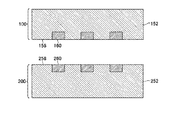
図1は、積層半導体装置400の一部をなす受光基板100の断面図である。受光基板100は、支持基板110、半導体ウェル130および多層配線層150を備える。
FIG. 1 is a cross-sectional view of a
支持基板110は、受光基板100の製造プロセスに耐える機械的強度を担う厚さを有する。支持基板110の一面には、絶縁層120を介して半導体ウェル130が配される。半導体ウェル130には、支持基板110の面方向に配列された複数のフォトダイオード132が配される。また、半導体ウェル130には、隣接して形成されたゲート電極140等により複数の電界効果トランジスタが形成される。
The
多層配線層150は、半導体ウェル130の表面に交互に積層された層間絶縁材152および配線材154により形成される。配線材154としては、チタン、タングステン等の金属材料を使用できる。層間絶縁材152は、珪素酸化物等により形成できる。
The
フォトダイオード132および電界効果トランジスタは、多層配線層150により相互に接続されて受光回路111を形成する。多層配線層150における配線材154の一端は、支持基板110と反対側の一面において外部に露出した接続パッド160に電気的に接続される。
The
受光回路111においては、フォトダイオード132の各々が画素に対応し、電界効果トランジスタが画素毎にリセット、選択および増幅を担う。フォトダイオード132が入射光を受けて蓄積した電荷は、電界効果トランジスタによるソースフォロワを通じて電圧信号として接続パッド160から外部に出力される。
In the
図2は、積層半導体装置400の一部をなす処理基板200の断面図である。処理基板200は、支持基板210、半導体ウェル230および多層配線層250を備える。
FIG. 2 is a cross-sectional view of the
支持基板210は、処理基板200の製造プロセスに耐える機械的強度を担う厚さを有する。支持基板210の一面には、半導体ウェル230が配される。半導体ウェル230には、半導体ウェル230に隣接して形成されたゲート電極240等により複数の電界効果トランジスタが作り込まれている。
The
多層配線層250は、半導体ウェル230の表面に交互に積層された層間絶縁材252および配線材254により形成される。複数の電界効果トランジスタは、多層配線層250により相互に接続されて処理回路211を形成する。
The
また、多層配線層250における配線材254の一端は、支持基板210と反対側の一面において外部に露出した接続パッド260に電気的に接続される。処理基板200の接続パッド260は、受光基板100と積層された場合に、受光基板100の接続パッド160に接続される。これにより、処理回路211が、受光基板100の受光回路111の出力信号を処理する。処理回路211においては、アナログ/デジタル変換、ノイズ抑圧、ファイル生成等の処理が実行される。
In addition, one end of the
更に、処理基板200は、支持基板210に嵌入した貫通電極256を有する。貫通電極256の一端は、多層配線層250の配線材254に電気的に接続される。貫通電極256の他端は、図示の段階では、支持基板210の内部に埋没している。
Further, the
図3は、イメージセンサとして用い得る積層半導体装置400を製造する過程で形成される積層基板300の断面図である。積層基板300において、受光基板100は、図1に示した状態に対して表裏が反転されて処理基板200に積層される。積層基板300においては、受光基板100の接続パッド160と、処理基板200の接続パッド260とが互いに当接して電気的に接続される。
FIG. 3 is a cross-sectional view of a
受光基板100および処理基板200を積層する場合は、それぞれの基板において予め定めた数箇所の位置合わせ指標の位置ずれに基づいて、受光基板100および処理基板200が位置合わせされる。位置合わせにおいては、例えば、全体の位置ずれが最小になる位置を算出するグローバルアライメント法により、積層基板300の歩留りを向上させることができる。更に、位置合わせ指標の位置に基づいて、オフセット補正、回転補正、直交度補正、スケーリング補正等を加えて、位置合わせ精度をより向上させることもできる。
When the
位置合わせの指標としては、接続パッド160、260そのものを利用してもよいし、受光基板100および処理基板200に形成された配線、基板等を利用してもよい。更に、位置合わせに利用する目的で受光基板100および処理基板200に設けたアライメントマークを利用してもよい。
As the alignment index, the
図4は、積層基板300を更に加工して作製された積層半導体装置400の断面図である。積層半導体装置400において、処理基板200の支持基板210は薄化され、図中下面に露出した貫通電極256の下端に、バンプ220が設けられる。これにより、積層半導体装置400は、他の基板、リードフレーム等に電気的に接続できる。
FIG. 4 is a cross-sectional view of a
また、積層半導体装置400において、受光基板100の支持基板110は除去され、露出した絶縁層120に、遮光層170、平坦化層172、有機平坦化層174、182、オンチップカラーフィルタ180およびオンチップレンズ190等が順次積層される。
In the
これにより、受光基板100のフォトダイオード132は、オンチップレンズ190およびオンチップカラーフィルタ180を通じて入射した光を、多層配線層150を通すことなく受光する。このように、積層半導体装置400は、裏面照射型イメージセンサを形成する。
Thereby, the
積層半導体装置400において、受光基板100および処理基板200は、接続パッド160、260を通じて電気的に結合されている。よって、受光基板100においてフォトダイオード132への入射光により発生した電荷は、電圧信号として処理基板200側の処理回路211に受け渡され、更に、デジタル変換等の処理を経て、バンプ220から外部に出力される。
In the
なお、受光基板100および処理基板200のそれぞれは、図1または図2に示した構造をそれぞれの面方向に繰り返し有する。よって、受光基板100および処理基板200を積層することにより、多数の積層半導体装置400が一括して製造される。
Each of the
よって、積層基板300は、ダイシングにより切り分けられて多数のダイとなる。こうして得られたダイのそれぞれは、受光基板100および処理基板200を積層して製造したことにより、高い歩留りと高い集積密度とを有する。
Therefore, the
図5から図8は、積層基板300の製造過程の一部を、受光基板100および処理基板200の接合段階に注目して詳細に示す模式的断面図である。図中においては、受光基板100および処理基板200を単純化して、絶縁物である層間絶縁材152、252と導体である接続パッド160、260とにより示している。
5 to 8 are schematic cross-sectional views showing in detail a part of the manufacturing process of the
図5に示すように、積層基板300の製造過程においては、受光基板100において層間絶縁材152の中に接続パッド160が露出した表面158と、処理基板200において層間絶縁材252の中に接続パッド260が露出した表面258とが接合される。続いて説明するように、受光基板100および処理基板200の接合においては、まず層間絶縁材152、252が相互に接合され、続いて接続パッド160、260が相互に接合される。
As shown in FIG. 5, in the manufacturing process of the
受光基板100および処理基板200の接合においては、まず、図6に示すように、受光基板100および処理基板200の表面を平滑化して、層間絶縁材152、252の表面に、接合面159、259を形成する。接合面159、259は、研磨によっても平滑化できるが、研磨に先立ってエッチングを併用してもよい。接合面159、259は、それぞれ1nm未満まで平滑化することが好ましい。平滑化された受光基板100および処理基板200は、研磨に伴って生じた残留物を洗浄により除去した後乾燥される。
In bonding the
なお、接合面159、259を研磨する場合、接合面159、259を形成する層間絶縁材152、252と、接続パッド160、260を形成する金属等との物性の相違により、接続パッド160、260の研磨量が、層間絶縁材152、252よりも多くなる。このため、研磨後は、接続パッド160、260の先端面が、接合面159、259の表面よりも、層間絶縁材152、252の内部に沈み込んでいる。
Note that, when the bonding surfaces 159 and 259 are polished, the
また、金属製の接続パッド160、260は、研磨される場合の圧力により不可避に弾性変形する。このため、研磨後の接続パッド160、260の先端表面は平坦ではなく、中央が窪んだ形状になる。
Further, the
次に、受光基板100および処理基板200の接合面159、259を活性化処理する。接合面159、259は、例えば、反応性イオンエッチング、誘導結合プラズマ等により接合面159、259の表面を処理して活性化できる。更に、活性化処理された接合面159、259を、NH4OH、NH4F、HF等の溶液に短時間浸漬する処理をしてもよい。
Next, the bonding surfaces 159 and 259 of the
こうして、絶縁体である層間絶縁材152、252の表面に形成された接合面159、259を活性化された受光基板100および処理基板200は、対向して接近させることにより、図7に示すように、自ずから吸着して接合され、積層基板300を形成する。更に、受光基板100および処理基板200が相互に吸着した状態で24時間程度静置することにより、受光基板100および処理基板200の接合強度は、支持基板110、210の化学機械研磨等の処理に耐え得るものとなる。
As shown in FIG. 7, the light-receiving
なお、図7に示した段階では、接合面159、259から沈み込んだ接続パッド160、260の間には間隙が残る。また、既に説明した通り、接続パッド160、260の先端表面は中央が窪んだ形状を有するので、接続パッド160、260相互の間隙は、中央においてより広い。このため、受光基板100と処理基板200との間に、十分な電気的接続はまだ形成されていない。
In the stage shown in FIG. 7, a gap remains between the
次に、積層基板300をリフロー処理することにより、図8に示すように、接続パッド160、260が一体化されて、接続部360が形成される。接続パッド160、260を、インジウム、錫−銀合金のように低温で溶融する材料で形成することにより、200度以下の低い温度で積層基板300をリフロー処理できる。こうして形成された接続部360は、受光基板100および処理基板200の間で、これら基板の厚さ方向に電気的接続を形成する。
Next, by reflowing the
接続部360が形成されてリフロー処理が完了すると、積層基板300は自然に冷却されて室温に戻る。金属により形成された接続部360と、絶縁物により形成された層間絶縁材152との間には熱膨張率に差がある。このため、冷却の過程で、接続部360がより大きく収縮し、積層基板300に熱応力が作用する。
When the
図中に誇張して描かれた陥没部155の形状が示すように、基板の熱応力は、接続部360が存在する位置において最も大きい。また、接続部360は、積層基板300の面方向について一定の間隔で複数配置されているので、積層基板300に作用する熱応力も、積層基板300の面方向に周期的に分布する。
As shown by the exaggerated shape of the
更に、図4に示したように、積層基板300を用いて形成された積層半導体装置400において、受光基板100側では支持基板210が取り除かれているが、処理基板200側では支持基板210の一部が残されている。このため、接続部360において生じた応力は、受光基板100においてより強く影響する。このため、受光基板100には、接続部360の配置に応じた周期的な光学特性の分布が生じる。
Furthermore, as shown in FIG. 4, in the
また、半導体に応力が作用した場合、抵抗値等の電気的特性が変化する。このため、接続部360により受光基板100に生じた応力が作用した場合、フォトダイオード132、電界効果トランジスタ等の半導体素子の特性も変化する。
In addition, when a stress is applied to the semiconductor, electrical characteristics such as a resistance value change. For this reason, when the stress generated on the
図9は、積層半導体装置400の模式的断面図であり、接続部360、フォトダイオード132およびゲート電極140の相対位置に着目して描かれている。なお、図面を簡潔にする目的で、配線層等の一部の断面は簡略化されている。
FIG. 9 is a schematic cross-sectional view of the stacked
積層半導体装置400においては、積層半導体装置400の面方向についてフォトダイオード132の各々と同じ位置に、換言すれば、積層半導体装置400の厚さ方向についてフォトダイオード132と重なる位置に、接続部360がそれぞれ配されている。これは、図1に示した受光基板100を製造する場合に、支持基板110の面方向について、フォトダイオード132と同じ位置に接続パッド160を形成したことを意味する。
In the
このような配置により、接続部360において生じた熱応力がフォトダイオード132を含む受光基板100全体に作用して、図8に示した陥没部155が生じた場合であっても、それにより生じた受光基板100の光学特性の変動は各フォトダイオード132に対して等しく作用する。よって、積層半導体装置400においては、熱応力に起因するフォトダイオード132の特性のばらつきが抑制される。
With such an arrangement, the thermal stress generated in the
更に、受光基板100においては、フォトダイオード132の各々に隣接して配置されたゲート電極140を含む電界効果トランジスタ等の半導体素子のそれぞれも、接続部360から等しい間隔をおいた位置に配される。このような配置により、接続部360において生じた熱応力が受光基板100全体に作用して半導体素子の容量値等が変動した場合であっても、その変動は周期的に配された半導体素子の全てに対して等しく作用する。よって、積層半導体装置400においては、周期的に配された半導体素子について、熱応力に起因する特性のばらつきが抑制される。
Furthermore, in the
図10は、図9に示した積層半導体装置400の一部を詳細に示す模式的断面図であり、接続部360に起因する熱応力の作用を誇張して描いている。図5から図8までを参照して説明したように、周囲と異なる材料で形成された接続部360の存在により、積層半導体装置400に熱応力が生じる場合がある。図10は、そのような熱応力の作用を、受光基板100に生じた厚さの変化により表している。
FIG. 10 is a schematic cross-sectional view showing a part of the stacked
図示のように、積層半導体装置400においては、受光基板100の厚さに周期的な変動が生じ、フォトダイオード132が設けられた位置に複数の陥没部155が形成されている。フォトダイオード132の各々は、オンチップレンズ190を通じて入射光を受光する。オンチップレンズ190は、受光基板100および処理基板200を接合した後に受光基板100の表面を平坦化して形成するので、陥没部155が生じている位置では、オンチップレンズ190とフォトダイオード132との間隔が広くなる。
As illustrated, in the stacked
フォトダイオード132と受光基板100の間隔が変化した場合は、オンチップレンズさ190を通じたフォトダイオード132の受光量も変化する。しかしながら、積層半導体装置400においては、接続部360とフォトダイオード132とが、受光基板100の面方向について同じ位置に配されているので、フォトダイオード132の各々は、いずれもが陥没部155の底部に位置している。
When the distance between the
これにより、図中の底面中央によりフォトダイオード132の各々の位置を代表させた場合、積層半導体装置400におけるフォトダイオード132の入射面は、単一の配列平面P1上に配列される。よって、フォトダイオード132に対して、オンチップレンズ190は同じ光学的作用を生じ、受光基板100の熱応力によるフォトダイオード132の光学特性のばらつきは抑制される。
Thus, when a representative of the respective positions of the
なお、受光基板100における熱応力の分布は、受光基板100の厚さの変動として現れるとは限らない。例えば、受光基板100の厚さが外見上均一であっても、受光基板100の屈折率に分布が生じている場合がある。また、フォトダイオード132以外の半導体素子においても、熱応力の分布が容量等のばらつきとして顕在化する場合がある。このような特性のばらつきも、フォトダイオード132と接続部360との位置関係を一定にすることにより抑制される。
The distribution of thermal stress in the
このように、積層半導体装置400においては、研磨、接合等に伴う処理により積層半導体装置400に不均一な応力が生じて光学特性に分布が形成される場合であっても、その原因となる接続部360とフォトダイオード132とを同じ位置に配することにより、当該分布を補償している。また、周期的に配置する半導体素子も、厚さが等しくなる位置に配置することにより特性のばらつきを抑制している。
As described above, in the
なお、上記の例では、フォトダイオード132と接続部360とを、受光基板100の面方向について同じ位置に配置した。しかしながら、フォトダイオード132と接続部360との位置が同じ位置に配されていない場合であっても、フォトダイオード132と接続部360との相対位置が一定であれば、上記の場合と同様に、熱応力がフォトダイオード132等に及ぼす影響が均一化され、特性のばらつきを抑制できる。
In the above example, the
図11は、他の積層半導体装置401の模式的断面図である。積層半導体装置401の受光基板101においては、接続部360のそれぞれが、積層半導体装置401の面方向についてそれぞれ隣あったフォトダイオード132の中間に配される。これにより、接続部360の配列周期と、フォトダイオード132の配列周期との比は2:1になる。
FIG. 11 is a schematic cross-sectional view of another stacked
フォトダイオード132および接続部360を上記のように配置することにより、熱応力の原因となる接続部360と、個々のフォトダイオード132との、受光基板101の面方向に係る相対位置は均一になる。よって、熱応力がフォトダイオード132に及ぼす影響も均一になり、熱応力に起因する受光基板101の特性の分布が補償される。
By disposing the
図12は、積層半導体装置401の模式的平面図である。積層半導体装置401の受光基板101はオンチップカラーフィルタを備えており、フォトダイオード132の各々は、互いに異なる特定の帯域、例えば、赤、青または緑のいずれかを含む帯域を選択的に受光するサブピクセルを形成する。
FIG. 12 is a schematic plan view of the stacked
また、積層半導体装置401においては、複数のサブピクセルを組み合わせてカラー画素134が形成される。図示の例では、カラー画素134の各々において、図中左下に位置して赤を含む帯域を受光するサブピクセルRと、図中右上に位置して青を含む帯域を受光するサブピクセルBと、図中左上および右下に位置して緑を含む帯域を受光するサブピクセルG1、G2とを組み合わせてひとつのカラー画素134が形成される。
In the
積層半導体装置401におけるカラー画素134に着目した場合、接続部360は、積層半導体装置401の面方向についてカラー画素134の中心と同じ位置に配される。これにより、カラー画素134の各々の内部において、接続部360により生じた応力は、4つのサブピクセルR、B、G1、G2に対して均等に作用する。これにより、カラー画素134の各々の内部における熱応力に起因するサブピクセルR、B、G1、G2相互の特性のばらつきは抑制される。
When attention is paid to the
図13は、図12に示した積層半導体装置401の一部を詳細に示す模式的断面図であり、接続部360に起因する熱応力の作用を誇張して描いている。積層半導体装置401のカラー画素134の各々においては、接続部360が、カラー画素134各々の中央であって、サブピクセルR、B、G1、G2を形成するフォトダイオード132相互の中間の位置に配されている。よって、フォトダイオード132の各々は、接続部360の熱膨張率差に起因して生じた陥没部155の斜面において、同じ高さになる部分に位置している。
FIG. 13 is a schematic cross-sectional view showing a part of the stacked
これにより、図中の底面中央によりフォトダイオード132の各々の位置を代表させた場合、積層半導体装置401におけるフォトダイオード132の入射面は、単一の配列平面P2上に配置される。よって、フォトダイオード132に対して、オンチップレンズ190は同じ光学的作用を生じ、熱応力によるフォトダイオード132の光学特性のばらつきは抑制される。
Thus, when a representative of the respective positions of the
このように、フォトダイオード132の配列周期と、接続部360の配列周期とを整数比にすることにより、接続部360により生じた応力がフォトダイオード132に及ぼす影響を、積層半導体装置401全体で均一にして、フォトダイオード132の特性を安定させることができる。上記の例では、説明のために配列周期の比が2:1の場合を示したが、イメージセンサにおけるフォトダイオード132の集積密度を考えると、配列周期の比は更に大きくなる場合もあり得る。
In this way, by setting the arrangement period of the
なお、積層半導体装置401は、図中左側に位置する最外側のフォトダイオード132よりも更に外側(図中左側)に追加された接続部360を備える。これにより、最外側のフォトダイオード132にも、他のフォトダイオード132と変わらない応力が作用する。積層半導体装置401においては、接続部360の配置の周期性を維持する目的で、電気的な接続には用いないダミーの接続部360を配置してもよい。
Note that the
図14は、積層半導体装置402の模式的断面図である。積層半導体装置401の受光基板101において、接続部360のそれぞれは、周期的に配された複数のフォトダイオード132のうち、隣り合った一対のフォトダイオード132の一方の直下に配される。これにより、接続部360の配列周期と、フォトダイオード132の配列周期との比は2:1となる。
FIG. 14 is a schematic cross-sectional view of the stacked
積層半導体装置402においては、複数のフォトダイオード132のうち、積層半導体装置402の面方向について、接続部360と同じ位置に配されたフォトダイオード132と、接続部360に対して一定の相対位置で配置されたフォトダイオード132とが混在する。これら2種類のフォトダイオード132に対しては、接続部360に起因する熱応力の作用も相互に異なる。しかしながら、積層半導体装置402全体では、受光基板102の面方向に係る熱応力の影響は略均一になる。よって、熱応力に起因する受光基板102の特性のばらつきが抑制される。
In the
図15は、積層半導体装置402の模式的平面図である。積層半導体装置402においても、積層半導体装置401と同様に、フォトダイオード132の各々はオンチップカラーフィルタによりサブピクセルを形成し、複数のサブピクセルがカラー画素134を形成する。
FIG. 15 is a schematic plan view of the stacked
積層半導体装置402においてひとつのカラー画素134に着目すると、積層半導体装置402においては、一方の緑のサブピクセルG1と赤のサブピクセルRとの中間に接続部360が配される。よって、図中に一点鎖線S1で示す断面においては、図13に示した積層半導体装置401のフォトダイオード132の場合と同様に、サブピクセルG1、Rを形成するフォトダイオード132が、単一の配列平面上に配置される。
When attention is paid to one
また、積層半導体装置402における他のサブピクセルB、G2を形成するフォトダイオード132は、図中に一点鎖線S2により示すように、接続部360が存在していない領域に配される。接続部360が存在していない領域では積層半導体装置402に光学特性の分布が生じないので、サブピクセルB、G2の特性にはばらつきが生じ難い。
Also, other sub-pixels B in the
更に、積層半導体装置402において特定の帯域に対応するフォトダイオード132、例えば、赤を含む帯域に対応するサブピクセルRを形成するフォトダイオード132に着目すると、積層半導体装置402全体で接続部360に対する相対位置は一定になる。よって、積層半導体装置402全体では、サブピクセルRの特性のばらつきが抑制される。同様に、他の帯域に対応するサブピクセルB、G1、G2に関しても、積層半導体装置402全体で特性のばらつきが抑制される。
Further, when attention is paid to the
このように、積層半導体装置402においては、接続部360がカラー画素134の位置に対して偏った配置となっているにもかかわらず、個々の種類のサブピクセルR、B、G1、G2に着目すると、接続部360に対する相対位置が一定に保たれている。また、個々の種類のサブピクセルR、B、G1、G2の配列周期は、接続部360の配列周期と整数比をなす。これにより、積層半導体装置402においても、接続部360により生じた応力がフォトダイオード132に及ぼす影響を、積層半導体装置402全体で均一にして、フォトダイオード132の特性を安定させることができる。
As described above, in the stacked
図16は、他の積層半導体装置403の断面図である。積層半導体装置403は、次に説明する部分を除くと、図4に示した積層半導体装置400と共通の構造を有する。よって、共通部分には同じ参照番号を付して重複する説明を省く。
FIG. 16 is a cross-sectional view of another stacked
積層半導体装置403は、互いに接合された受光基板103および処理基板201を含む。受光基板103は、図4に示した受光基板100における接続パッド160に代えてバンプ162を有する。処理基板201は、図4に示した処理基板200における接続パッド260に代えてバンプ262を有する。積層半導体装置403においては、これらのバンプ162、262が、受光基板103と処理基板201とを電気的に接続している。
The
図17から図19は、積層半導体装置403の製造過程の一部を、受光基板100および処理基板200の接合段階に注目して詳細に示す模式的断面図である。図中において、受光基板103および処理基板201を単純化して示している。
17 to 19 are schematic cross-sectional views showing in detail a part of the manufacturing process of the
図17に示すように、積層半導体装置403を製造する場合は、受光基板100の図中下面、即ち、処理基板201に接合する側の表面158に、突出したバンプ162を形成する。また、処理基板201の上面、即ち、受光基板103に接合する側の表面258にもバンプ262を形成する。バンプ162、262は、はんだ等の金属により形成できる。
As shown in FIG. 17, when manufacturing the
次に、図18に示すように、受光基板103および処理基板201を重ねてバンプ162、262どうしを当接させた状態で、加圧または加熱加圧して、バンプ162、262を融合させる。これにより、受光基板103および処理基板201の間には基板の厚さ方向の電気的接続が形成され、受光基板103および処理基板201は積層基板301となる。
Next, as shown in FIG. 18, in a state where the
なお、少なくとも、上記のように受光基板103および処理基板201を接合するまでの段階では、受光基板103および処理基板201のそれぞれに、支持基板110、210が残されている。これにより、受光基板103および処理基板201のそれぞれは、接合に係る機械的な負荷に耐えることができる。
Note that the
図16に示した積層半導体装置403を製造する場合、受光基板103および処理基板201を接合した後に、受光基板103の支持基板110を除去し、処理基板201の支持基板210を薄化する。支持基板110、210は、例えば、化学機械研磨により除去または薄化される。
When the
化学機械研磨においては、研磨工具から支持基板110、210にかかる圧力も、研磨効率に影響する。一方、積層基板301においては、支持基板110、210の研磨される面に対する裏面が、バンプ162、262に支持された領域と、バンプ162、262が存在せずに浮いた領域とがある。このため、平坦な研磨工具を用いても、支持基板110、210の研磨量に分布が生じる。
In chemical mechanical polishing, the pressure applied from the polishing tool to the
図19は、受光基板103の支持基板110を研磨した後の状態を示す模式的断面図である。図示のように、バンプ162、262が存在する領域は、バンプ162、262により裏面から強固に支持されるので、研磨効率が上昇して研磨量が増加する。これに対して、バンプ162、262が存在しない領域は、研磨量が少ない。このため、積層半導体装置402の面方向について、バンプ162、262が存在する領域には陥没部155が形成される。
FIG. 19 is a schematic cross-sectional view showing a state after the
このように、バンプ162、262により接合された受光基板103および処理基板201を有する積層基板301を研磨した場合、基板に厚さの分布が生じる。このため、入射光を透過させる受光基板103においては、受光基板103および処理基板201の厚さの分布に応じて光学特性が変化する。また、受光基板103および処理基板201含まれる半導体素子の特性も、基板の厚さの分布に応じて変化する。
Thus, when the
図20は、積層半導体装置403の模式的断面図であり、積層半導体装置403の面方向について、バンプ162、262、フォトダイオード132およびゲート電極140の相対位置に着目して描かれている。図面を簡潔にする目的で、配線層等の一部の断面は簡略化されている。
FIG. 20 is a schematic cross-sectional view of the
積層半導体装置403においては、積層半導体装置403の面方向についてフォトダイオード132と同じ位置に、換言すれば、積層半導体装置403の厚さ方向についてフォトダイオード132と重なる位置に、バンプ162、262が配されている。よって、支持基板110、210の研磨により生じる厚さ分布の周期と、基板の光学的特性の影響を受けるフォトダイオード132の配列周期とが一致する。これにより、フォトダイオード132の特性のばらつきが抑制される。
In the
同様に、フォトダイオード132の各々に隣接して配置された電界効果トランジスタ等の半導体素子のそれぞれも、基板の厚さ分布の周期と等しい周期で配置される。よって、半導体素子の特性のばらつきも抑制される。
Similarly, each semiconductor element such as a field effect transistor arranged adjacent to each of the
図21は、他の積層半導体装置404の模式的断面図である。積層半導体装置404においては、受光基板104および処理基板202が、バンプ162、262により接合されている。
FIG. 21 is a schematic cross-sectional view of another stacked
積層半導体装置404におけるバンプ162、262は、積層半導体装置404の面方向について、それぞれ隣あったフォトダイオード132の中間に配される。これにより、バンプ162、262の配列周期は、フォトダイオード132の配列周期のちょうど2倍になる。よって、バンプ162、262の存在により生じた厚さ分布による光学特性の変化は、フォトダイオード132の各々に対して等しく影響し、フォトダイオード132の特性のばらつきは抑制される。
The
図22は、また他の積層半導体装置405の模式的断面図である。積層半導体装置405においては、受光基板105および処理基板203が、バンプ162、262により接合されている。
FIG. 22 is a schematic cross-sectional view of another stacked
積層半導体装置405の受光基板105においては、隣接する一対のフォトダイオード132の一方の直下に接続部360が配される。ただし、積層半導体装置405は、図15に示した積層半導体装置402の受光基板102と同様に、ベイヤー配列のオンチップカラーフィルタ180を備えてカラーイメージセンサを形成する。よって、各帯域に対応したサブピクセルに着目すると、フォトダイオード132は、積層半導体装置402の面方向について、バンプ162、262に対して一定の相対位置を有する。よって、基板の厚さの分布に起因するフォトダイオード132の特性のばらつきは抑制される。
In the
図23は、また、他の積層半導体装置406の模式的断面図である。図23は、積層半導体装置406における処理基板200側に着目して描かれている。
FIG. 23 is a schematic cross-sectional view of another stacked
積層半導体装置406においても、接続部360からの熱応力が多層配線層250を通じて半導体ウェル230に作用する。しかしながら、既に説明したように、処理基板200は、支持基板210の一部に支持されて高い剛性を有する。よって、接続部360の熱応力は、専ら受光基板100に影響する。
Also in the
一方、処理基板200は、支持基板210を貫通して、支持基板210の厚さ方向に電気的接続を形成する貫通電極256を有する。貫通電極256は、厚い支持基板210を貫通する長さを有するので、処理基板200の半導体ウェル230に応力を及ぼす。
On the other hand, the
そこで、積層半導体装置406の処理基板では、電界効果トランジスタ等の半導体素子を形成するゲート電極240を、積層半導体装置406の面方向について、貫通電極256の直近の位置に、貫通電極256と同じ数配置している。これにより、貫通電極256から半導体素子に作用する応力は略均一になり、支持基板210の応力分布に起因する半導体素子の特性のばらつきが抑制される。
Therefore, in the processing substrate of the stacked
図24は、また他の積層半導体装置407の模式的断面図である。図24は、積層半導体装置407における処理基板204に着目して描かれている。
FIG. 24 is a schematic cross-sectional view of another stacked
積層半導体装置407の処理基板204においては、貫通電極256のそれぞれが、積層半導体装置407の面方向についてそれぞれ隣あったゲート電極240の中間に配される。これにより、貫通電極256の配列周期は、半導体素子の配列周期の2倍になる。しかしながら、貫通電極256の各々からゲート電極240までの間隔はいずれも等しい。よって、貫通電極256により生じた応力は、半導体素子の各々に対して等しく作用し、半導体素子の特性のばらつきが抑制される。
In the
なお、処理基板204に形成される処理回路211の構造は、受光基板100に形成される受光回路111に比較すると周期性が低い。しかしながら、特性を揃えることが望ましい一部の半導体素子を選択して、貫通電極256から等間隔になる位置に配置することにより、素子特性のばらつきを抑制できる。
Note that the structure of the
また、フォトダイオード132、ゲート電極240、接続部360等の配置の周期性が、積層半導体装置400、401、402、403、404、405、406、407全体で一定ではない場合であっても、例えば、特性を揃えることが望ましい半導体素子を、接続部360の配置間隔が等しい領域に配置することにより、特性のばらつきを抑制できる。更に、半導体素子の特性のばらつきを抑制する目的で、接続部360の配置間隔を調整してもよい。また更に、半導体素子の特性のばらつきを抑制する目的で、電気的接続には用いないダミーの接続部360を配置してもよい。
Further, even when the periodicity of the arrangement of the
以上、本発明を実施の形態を用いて説明したが、本発明の技術的範囲は上記実施の形態に記載の範囲には限定されない。上記実施の形態に、多様な変更または改良を加えることが可能であることが当業者に明らかである。その様な変更または改良を加えた形態も本発明の技術的範囲に含まれ得ることが、特許請求の範囲の記載から明らかである。 As mentioned above, although this invention was demonstrated using embodiment, the technical scope of this invention is not limited to the range as described in the said embodiment. It will be apparent to those skilled in the art that various modifications or improvements can be added to the above-described embodiment. It is apparent from the scope of the claims that the embodiments added with such changes or improvements can be included in the technical scope of the present invention.
100、101、102、103、104、105 受光基板、110、210 支持基板、111 受光回路、120 絶縁層、130、230 半導体ウェル、132 フォトダイオード、134 カラー画素、140、240 ゲート電極、150、250 多層配線層、152、252 層間絶縁材、154、254 配線材、155 陥没部、158、258 表面、159、259 接合面、160、260 接続パッド、162、220、262 バンプ、170 遮光層、172 平坦化層、174、182 有機平坦化層、180 オンチップカラーフィルタ、190 オンチップレンズ、200、201、202、203、204 処理基板、211 処理回路、256 貫通電極、300、301 積層基板、360 接続部、400、401、402、403、404、405、406、407 積層半導体装置 100, 101, 102, 103, 104, 105 Light receiving substrate, 110, 210 Support substrate, 111 Light receiving circuit, 120 Insulating layer, 130, 230 Semiconductor well, 132 Photodiode, 134 Color pixel, 140, 240 Gate electrode, 150, 250 Multilayer wiring layer, 152, 252 Interlayer insulating material, 154, 254 Wiring material, 155 Depressed part, 158, 258 Surface, 159, 259 Bonding surface, 160, 260 Connection pad, 162, 220, 262 Bump, 170 Light shielding layer, 172 planarization layer, 174, 182 organic planarization layer, 180 on-chip color filter, 190 on-chip lens, 200, 201, 202, 203, 204 processing substrate, 211 processing circuit, 256 through electrode, 300, 301 multilayer substrate, 360 connections, 400, 401, 402, 403, 404, 405, 406, 407 Multilayer semiconductor device
Claims (12)
前記基板には、他の基板への前記基板の積層により起伏が生じ、
前記複数の受光素子の光学条件は、前記起伏により変化し、
前記複数の受光素子の各々は、前記起伏が生じたときの前記光学条件が等しくなる位置に配置され、
前記基板と他の基板との電気的な接続を形成する複数の接続部を備え、
前記複数の受光素子の少なくとも一つと前記複数の接続部の少なくとも一つとの相対位置が、前記複数の受光素子の他の少なくとも一つと前記複数の接続部の他の少なくとも一つとの相対位置と同じになるように、前記複数の受光素子が配置されており、
前記複数の受光素子は、それぞれ前記複数の接続部のいずれかと、前記面方向について同じ位置に配され、
前記面方向において、前記起伏の分布周期と前記複数の受光素子の配列周期との比の値が、1を除く整数である半導体装置。 A semiconductor device comprising a substrate and a plurality of light receiving elements formed in the surface direction of the substrate,
In the substrate, undulation occurs by stacking the substrate on another substrate,
The optical conditions of the plurality of light receiving elements change due to the undulations,
Each of the plurality of light receiving elements is disposed at a position where the optical conditions are equal when the undulation occurs .
A plurality of connecting portions for forming an electrical connection between the substrate and another substrate;
A relative position between at least one of the plurality of light receiving elements and at least one of the plurality of connection portions is the same as a relative position between at least one of the plurality of light receiving elements and at least one other of the plurality of connection portions. The plurality of light receiving elements are arranged so that
The plurality of light receiving elements are respectively disposed at the same position with respect to any one of the plurality of connection portions and the surface direction,
A semiconductor device, wherein a value of a ratio between the undulation distribution period and the arrangement period of the plurality of light receiving elements is an integer other than 1 in the plane direction .
前記光学条件は、前記複数の受光素子と前記レンズとの間隔であり、前記複数の受光素子は、前記間隔が等しくなるように配置されている請求項1または2に記載の半導体装置。 A lens disposed above the plurality of light receiving elements;
The semiconductor device according to claim 1, wherein the optical condition is an interval between the plurality of light receiving elements and the lens, and the plurality of light receiving elements are arranged so that the intervals are equal.
前記複数の受光素子は、前記複数の陥没部内、および、前記複数の陥没部の間のいずれか一方に配置されており、他方には配置されていない請求項1から3のいずれか一項に記載の半導体装置。 The undulation has a plurality of depressions;
Wherein the plurality of light receiving elements, the plurality of recessed portion, and are arranged in one of between the plurality of depressions, from claim 1 and the other not located in any one of 3 The semiconductor device described.
前記基板には、他の基板への前記基板の積層により応力が生じ、
前記複数の受光素子の光学条件は、前記応力により変化し、
前記複数の受光素子の各々は、前記応力が生じたときの前記光学条件が等しくなる位置に配置され、
前記基板と他の基板との電気的な接続を形成する複数の接続部を備え、
前記複数の受光素子の少なくとも一つと前記複数の接続部の少なくとも一つとの相対位置が、前記複数の受光素子の他の少なくとも一つと前記複数の接続部の他の少なくとも一つとの相対位置と同じになるように、前記複数の受光素子が配置されており、
前記複数の受光素子は、それぞれ前記複数の接続部のいずれかと、前記面方向について同じ位置に配され、
前記面方向において、前記応力の分布周期と前記複数の受光素子の配列周期との比の値が、1を除く整数である半導体装置。 A semiconductor device comprising a substrate and a plurality of light receiving elements arranged in a surface direction of the substrate,
In the substrate, stress is generated by stacking the substrate on another substrate,
The optical conditions of the plurality of light receiving elements are changed by the stress,
Each of the plurality of light receiving elements is disposed at a position where the optical conditions are equal when the stress is generated ,
A plurality of connecting portions for forming an electrical connection between the substrate and another substrate;
A relative position between at least one of the plurality of light receiving elements and at least one of the plurality of connection portions is the same as a relative position between at least one of the plurality of light receiving elements and at least one other of the plurality of connection portions. The plurality of light receiving elements are arranged so that
The plurality of light receiving elements are respectively disposed at the same position with respect to any one of the plurality of connection portions and the surface direction,
A semiconductor device, wherein a value of a ratio between a distribution period of the stress and an arrangement period of the plurality of light receiving elements is an integer excluding 1 in the plane direction .
前記複数の半導体素子の各々は、前記基板を他の基板に積層した場合に前記基板に生じる応力が等しく作用する位置に配置され、
前記基板と他の基板との電気的な接続を形成する複数の接続部を備え、
前記複数の半導体素子の少なくとも一つと前記複数の接続部の少なくとも一つとの相対位置が、前記複数の半導体素子の他の少なくとも一つと前記複数の接続部の他の少なくとも一つとの相対位置と同じになるように、前記複数の半導体素子が配置されており、
前記複数の半導体素子は、それぞれ前記複数の接続部のいずれかと、前記面方向について同じ位置に配され、
前記面方向において、前記応力の分布周期と前記複数の半導体素子の配列周期との比の値が、1を除く整数である半導体装置。 A semiconductor device comprising a substrate and a plurality of semiconductor elements arranged in a surface direction of the substrate,
Each of the plurality of semiconductor elements is disposed at a position where stress generated in the substrate acts equally when the substrate is stacked on another substrate ,
A plurality of connecting portions for forming an electrical connection between the substrate and another substrate;
A relative position between at least one of the plurality of semiconductor elements and at least one of the plurality of connection portions is the same as a relative position between at least one other of the plurality of semiconductor elements and at least one other of the plurality of connection portions. The plurality of semiconductor elements are arranged so that
Each of the plurality of semiconductor elements is arranged at the same position as any one of the plurality of connection portions in the plane direction,
A semiconductor device, wherein a value of a ratio between a distribution period of the stress and an arrangement period of the plurality of semiconductor elements is an integer other than 1 in the plane direction .
前記複数の半導体素子の少なくとも一つと前記複数の接続部のいずれか一つとの相対位置が、前記複数の半導体素子の他の少なくとも一つと前記複数の接続部の他のいずれか一つとの相対位置と同じになるように、前記複数の半導体素子が配置されている請求項11に記載の半導体装置。 A plurality of connecting portions for forming connections in the thickness direction of the substrate;
A relative position between at least one of the plurality of semiconductor elements and any one of the plurality of connection portions is a relative position between at least one other of the plurality of semiconductor elements and any one of the plurality of connection portions. The semiconductor device according to claim 11 , wherein the plurality of semiconductor elements are arranged so as to be the same.
Priority Applications (1)
| Application Number | Priority Date | Filing Date | Title |
|---|---|---|---|
| JP2013036820A JP6307791B2 (en) | 2013-02-27 | 2013-02-27 | Semiconductor device |
Applications Claiming Priority (1)
| Application Number | Priority Date | Filing Date | Title |
|---|---|---|---|
| JP2013036820A JP6307791B2 (en) | 2013-02-27 | 2013-02-27 | Semiconductor device |
Publications (3)
| Publication Number | Publication Date |
|---|---|
| JP2014165417A JP2014165417A (en) | 2014-09-08 |
| JP2014165417A5 JP2014165417A5 (en) | 2017-03-30 |
| JP6307791B2 true JP6307791B2 (en) | 2018-04-11 |
Family
ID=51615738
Family Applications (1)
| Application Number | Title | Priority Date | Filing Date |
|---|---|---|---|
| JP2013036820A Active JP6307791B2 (en) | 2013-02-27 | 2013-02-27 | Semiconductor device |
Country Status (1)
| Country | Link |
|---|---|
| JP (1) | JP6307791B2 (en) |
Families Citing this family (6)
| Publication number | Priority date | Publication date | Assignee | Title |
|---|---|---|---|---|
| US10665623B2 (en) | 2015-02-27 | 2020-05-26 | Sony Corporation | Semiconductor device, solid-state image pickup element, imaging device, and electronic apparatus |
| CN107615481B (en) | 2015-05-18 | 2020-07-21 | 索尼公司 | Semiconductor device and imaging device |
| US10020336B2 (en) | 2015-12-28 | 2018-07-10 | Semiconductor Energy Laboratory Co., Ltd. | Imaging device and electronic device using three dimentional (3D) integration |
| CN107179575B (en) * | 2016-03-09 | 2022-05-24 | 松下知识产权经营株式会社 | Optical detection device and optical detection system |
| JP6761974B2 (en) * | 2016-03-09 | 2020-09-30 | パナソニックIpマネジメント株式会社 | Photodetector and photodetector |
| JP2018117027A (en) * | 2017-01-18 | 2018-07-26 | ソニーセミコンダクタソリューションズ株式会社 | Solid-state imaging element, electronic device, and method for manufacturing solid-state imaging element |
Family Cites Families (8)
| Publication number | Priority date | Publication date | Assignee | Title |
|---|---|---|---|---|
| JPH09181985A (en) * | 1995-12-22 | 1997-07-11 | Sony Corp | Ccd image pickup device and its manufacture |
| JP4349232B2 (en) * | 2004-07-30 | 2009-10-21 | ソニー株式会社 | Semiconductor module and MOS solid-state imaging device |
| KR100610481B1 (en) * | 2004-12-30 | 2006-08-08 | 매그나칩 반도체 유한회사 | Image sensor with enlarged photo detecting area and method for fabrication thereof |
| JP2008227253A (en) * | 2007-03-14 | 2008-09-25 | Fujifilm Corp | Back irradiation type solid-state image pickup element |
| JP5517800B2 (en) * | 2010-07-09 | 2014-06-11 | キヤノン株式会社 | Member for solid-state imaging device and method for manufacturing solid-state imaging device |
| JP5500007B2 (en) * | 2010-09-03 | 2014-05-21 | ソニー株式会社 | Solid-state imaging device and camera system |
| JP5835963B2 (en) * | 2011-06-24 | 2015-12-24 | オリンパス株式会社 | Solid-state imaging device, imaging device, and signal readout method |
| JP5791982B2 (en) * | 2011-07-06 | 2015-10-07 | オリンパス株式会社 | Solid-state imaging device, imaging device, and signal readout method |
-
2013
- 2013-02-27 JP JP2013036820A patent/JP6307791B2/en active Active
Also Published As
| Publication number | Publication date |
|---|---|
| JP2014165417A (en) | 2014-09-08 |
Similar Documents
| Publication | Publication Date | Title |
|---|---|---|
| JP6307791B2 (en) | Semiconductor device | |
| JP5247185B2 (en) | Back-illuminated image sensor and method for manufacturing the image sensor | |
| US8896079B2 (en) | Camera module having a light shieldable layer | |
| US8500344B2 (en) | Compact camera module and method for fabricating the same | |
| TW201919252A (en) | Semiconductor image sensor | |
| US10497733B2 (en) | Photoelectric conversion apparatus and system | |
| JP5970747B2 (en) | Semiconductor device | |
| US20110169118A1 (en) | Optical device, method of manufacturing the same, and electronic apparatus | |
| JP2012204403A (en) | Solid-state imaging device and method of manufacturing the same | |
| JP2014107448A (en) | Laminated semiconductor device manufacturing method and laminated semiconductor manufacturing apparatus | |
| JP2008052004A (en) | Lens array and method for manufacturing solid-state image pickup element | |
| JPWO2012073402A1 (en) | Solid-state imaging device and manufacturing method thereof | |
| US20230187460A1 (en) | Semiconductor package | |
| JP2018032792A (en) | Photoelectric conversion device and camera | |
| JP6168366B2 (en) | SEMICONDUCTOR DEVICE, SEMICONDUCTOR DEVICE MANUFACTURING METHOD, AND ELECTRONIC DEVICE | |
| US20160172401A1 (en) | Solid-state imaging device, camera module, and method for manufacturing solid-state imaging device | |
| JP5286820B2 (en) | Manufacturing method of solid-state imaging device | |
| JP5703784B2 (en) | Substrate connection structure, substrate set, optical sensor array device, and method of connecting substrates | |
| JP5864082B2 (en) | CMOS image sensor and manufacturing method thereof | |
| JP7246136B2 (en) | Semiconductor device, camera, and method for manufacturing semiconductor device | |
| US8158452B2 (en) | Backside-illuminated imaging device and manufacturing method of the same | |
| WO2016132616A1 (en) | Infrared detection device | |
| KR102059233B1 (en) | Semiconductor photodetection device | |
| JP6127747B2 (en) | Infrared sensor and method of manufacturing infrared sensor | |
| US11444220B2 (en) | Light detection device and method for manufacturing light detection device |
Legal Events
| Date | Code | Title | Description |
|---|---|---|---|
| A521 | Request for written amendment filed |
Free format text: JAPANESE INTERMEDIATE CODE: A523 Effective date: 20160209 |
|
| A621 | Written request for application examination |
Free format text: JAPANESE INTERMEDIATE CODE: A621 Effective date: 20160209 |
|
| A521 | Request for written amendment filed |
Free format text: JAPANESE INTERMEDIATE CODE: A523 Effective date: 20170224 |
|
| A131 | Notification of reasons for refusal |
Free format text: JAPANESE INTERMEDIATE CODE: A131 Effective date: 20170314 |
|
| A521 | Request for written amendment filed |
Free format text: JAPANESE INTERMEDIATE CODE: A523 Effective date: 20170510 |
|
| A131 | Notification of reasons for refusal |
Free format text: JAPANESE INTERMEDIATE CODE: A131 Effective date: 20170704 |
|
| A521 | Request for written amendment filed |
Free format text: JAPANESE INTERMEDIATE CODE: A523 Effective date: 20170824 |
|
| A02 | Decision of refusal |
Free format text: JAPANESE INTERMEDIATE CODE: A02 Effective date: 20171024 |
|
| A521 | Request for written amendment filed |
Free format text: JAPANESE INTERMEDIATE CODE: A523 Effective date: 20180119 |
|
| A911 | Transfer to examiner for re-examination before appeal (zenchi) |
Free format text: JAPANESE INTERMEDIATE CODE: A911 Effective date: 20180129 |
|
| TRDD | Decision of grant or rejection written | ||
| A01 | Written decision to grant a patent or to grant a registration (utility model) |
Free format text: JAPANESE INTERMEDIATE CODE: A01 Effective date: 20180213 |
|
| A61 | First payment of annual fees (during grant procedure) |
Free format text: JAPANESE INTERMEDIATE CODE: A61 Effective date: 20180226 |
|
| R150 | Certificate of patent or registration of utility model |
Ref document number: 6307791 Country of ref document: JP Free format text: JAPANESE INTERMEDIATE CODE: R150 |
|
| R250 | Receipt of annual fees |
Free format text: JAPANESE INTERMEDIATE CODE: R250 |
|
| R250 | Receipt of annual fees |
Free format text: JAPANESE INTERMEDIATE CODE: R250 |
|
| R250 | Receipt of annual fees |
Free format text: JAPANESE INTERMEDIATE CODE: R250 |
|
| R250 | Receipt of annual fees |
Free format text: JAPANESE INTERMEDIATE CODE: R250 |