JP5451547B2 - Solid-state imaging device - Google Patents
Solid-state imaging device Download PDFInfo
- Publication number
- JP5451547B2 JP5451547B2 JP2010156926A JP2010156926A JP5451547B2 JP 5451547 B2 JP5451547 B2 JP 5451547B2 JP 2010156926 A JP2010156926 A JP 2010156926A JP 2010156926 A JP2010156926 A JP 2010156926A JP 5451547 B2 JP5451547 B2 JP 5451547B2
- Authority
- JP
- Japan
- Prior art keywords
- solid
- film
- imaging device
- state imaging
- conductor
- Prior art date
- Legal status (The legal status is an assumption and is not a legal conclusion. Google has not performed a legal analysis and makes no representation as to the accuracy of the status listed.)
- Active
Links
- 238000003384 imaging method Methods 0.000 title claims description 64
- 239000010410 layer Substances 0.000 claims description 140
- 238000009792 diffusion process Methods 0.000 claims description 110
- 239000000758 substrate Substances 0.000 claims description 79
- 239000010949 copper Substances 0.000 claims description 68
- 229910052802 copper Inorganic materials 0.000 claims description 68
- RYGMFSIKBFXOCR-UHFFFAOYSA-N Copper Chemical compound [Cu] RYGMFSIKBFXOCR-UHFFFAOYSA-N 0.000 claims description 66
- 239000011229 interlayer Substances 0.000 claims description 56
- 230000002265 prevention Effects 0.000 claims description 56
- 230000004888 barrier function Effects 0.000 claims description 52
- 229910052751 metal Inorganic materials 0.000 claims description 49
- 239000002184 metal Substances 0.000 claims description 49
- 239000004020 conductor Substances 0.000 claims description 41
- 238000006243 chemical reaction Methods 0.000 claims description 31
- 230000002093 peripheral effect Effects 0.000 claims description 30
- 230000003321 amplification Effects 0.000 claims description 14
- 238000003199 nucleic acid amplification method Methods 0.000 claims description 14
- 229910052581 Si3N4 Inorganic materials 0.000 claims description 8
- 229910052782 aluminium Inorganic materials 0.000 claims description 8
- XAGFODPZIPBFFR-UHFFFAOYSA-N aluminium Chemical compound [Al] XAGFODPZIPBFFR-UHFFFAOYSA-N 0.000 claims description 8
- HQVNEWCFYHHQES-UHFFFAOYSA-N silicon nitride Chemical compound N12[Si]34N5[Si]62N3[Si]51N64 HQVNEWCFYHHQES-UHFFFAOYSA-N 0.000 claims description 8
- 229910045601 alloy Inorganic materials 0.000 claims description 5
- 239000000956 alloy Substances 0.000 claims description 5
- HBMJWWWQQXIZIP-UHFFFAOYSA-N silicon carbide Chemical compound [Si+]#[C-] HBMJWWWQQXIZIP-UHFFFAOYSA-N 0.000 claims description 4
- 229910010271 silicon carbide Inorganic materials 0.000 claims description 4
- 239000004065 semiconductor Substances 0.000 description 47
- 238000000034 method Methods 0.000 description 27
- 238000004519 manufacturing process Methods 0.000 description 15
- 238000005304 joining Methods 0.000 description 11
- 230000009977 dual effect Effects 0.000 description 10
- 230000004048 modification Effects 0.000 description 7
- 238000012986 modification Methods 0.000 description 7
- 238000005530 etching Methods 0.000 description 6
- WFKWXMTUELFFGS-UHFFFAOYSA-N tungsten Chemical compound [W] WFKWXMTUELFFGS-UHFFFAOYSA-N 0.000 description 6
- 239000010937 tungsten Substances 0.000 description 6
- 229910052721 tungsten Inorganic materials 0.000 description 6
- VYPSYNLAJGMNEJ-UHFFFAOYSA-N Silicium dioxide Chemical compound O=[Si]=O VYPSYNLAJGMNEJ-UHFFFAOYSA-N 0.000 description 5
- XUIMIQQOPSSXEZ-UHFFFAOYSA-N Silicon Chemical compound [Si] XUIMIQQOPSSXEZ-UHFFFAOYSA-N 0.000 description 5
- 238000002955 isolation Methods 0.000 description 5
- 150000002739 metals Chemical class 0.000 description 5
- 229910052710 silicon Inorganic materials 0.000 description 5
- 239000010703 silicon Substances 0.000 description 5
- 229910052814 silicon oxide Inorganic materials 0.000 description 5
- 239000011347 resin Substances 0.000 description 4
- 229920005989 resin Polymers 0.000 description 4
- 230000003071 parasitic effect Effects 0.000 description 3
- 229910052715 tantalum Inorganic materials 0.000 description 3
- GUVRBAGPIYLISA-UHFFFAOYSA-N tantalum atom Chemical compound [Ta] GUVRBAGPIYLISA-UHFFFAOYSA-N 0.000 description 3
- MZLGASXMSKOWSE-UHFFFAOYSA-N tantalum nitride Chemical compound [Ta]#N MZLGASXMSKOWSE-UHFFFAOYSA-N 0.000 description 3
- 238000010586 diagram Methods 0.000 description 2
- 239000012535 impurity Substances 0.000 description 2
- 238000005498 polishing Methods 0.000 description 2
- 230000035945 sensitivity Effects 0.000 description 2
- 239000000126 substance Substances 0.000 description 2
- VYZAMTAEIAYCRO-UHFFFAOYSA-N Chromium Chemical compound [Cr] VYZAMTAEIAYCRO-UHFFFAOYSA-N 0.000 description 1
- 230000004913 activation Effects 0.000 description 1
- 230000015572 biosynthetic process Effects 0.000 description 1
- 229910052804 chromium Inorganic materials 0.000 description 1
- 239000011651 chromium Substances 0.000 description 1
- 238000011109 contamination Methods 0.000 description 1
- 238000000151 deposition Methods 0.000 description 1
- 238000001312 dry etching Methods 0.000 description 1
- 239000010408 film Substances 0.000 description 1
- 239000007789 gas Substances 0.000 description 1
- PCHJSUWPFVWCPO-UHFFFAOYSA-N gold Chemical compound [Au] PCHJSUWPFVWCPO-UHFFFAOYSA-N 0.000 description 1
- 229910052737 gold Inorganic materials 0.000 description 1
- 239000010931 gold Substances 0.000 description 1
- 239000011261 inert gas Substances 0.000 description 1
- 239000012212 insulator Substances 0.000 description 1
- 230000007257 malfunction Effects 0.000 description 1
- WPBNNNQJVZRUHP-UHFFFAOYSA-L manganese(2+);methyl n-[[2-(methoxycarbonylcarbamothioylamino)phenyl]carbamothioyl]carbamate;n-[2-(sulfidocarbothioylamino)ethyl]carbamodithioate Chemical compound [Mn+2].[S-]C(=S)NCCNC([S-])=S.COC(=O)NC(=S)NC1=CC=CC=C1NC(=S)NC(=O)OC WPBNNNQJVZRUHP-UHFFFAOYSA-L 0.000 description 1
- 229910052758 niobium Inorganic materials 0.000 description 1
- 239000010955 niobium Substances 0.000 description 1
- GUCVJGMIXFAOAE-UHFFFAOYSA-N niobium atom Chemical compound [Nb] GUCVJGMIXFAOAE-UHFFFAOYSA-N 0.000 description 1
- 238000000059 patterning Methods 0.000 description 1
- 238000000206 photolithography Methods 0.000 description 1
- 229920002120 photoresistant polymer Polymers 0.000 description 1
- 229910021420 polycrystalline silicon Inorganic materials 0.000 description 1
- 229920005591 polysilicon Polymers 0.000 description 1
- 230000001681 protective effect Effects 0.000 description 1
- 239000002002 slurry Substances 0.000 description 1
Images


Classifications
-
- H—ELECTRICITY
- H01—ELECTRIC ELEMENTS
- H01L—SEMICONDUCTOR DEVICES NOT COVERED BY CLASS H10
- H01L27/00—Devices consisting of a plurality of semiconductor or other solid-state components formed in or on a common substrate
- H01L27/14—Devices consisting of a plurality of semiconductor or other solid-state components formed in or on a common substrate including semiconductor components sensitive to infrared radiation, light, electromagnetic radiation of shorter wavelength or corpuscular radiation and specially adapted either for the conversion of the energy of such radiation into electrical energy or for the control of electrical energy by such radiation
- H01L27/144—Devices controlled by radiation
- H01L27/146—Imager structures
- H01L27/14601—Structural or functional details thereof
- H01L27/14636—Interconnect structures
-
- H—ELECTRICITY
- H01—ELECTRIC ELEMENTS
- H01L—SEMICONDUCTOR DEVICES NOT COVERED BY CLASS H10
- H01L24/00—Arrangements for connecting or disconnecting semiconductor or solid-state bodies; Methods or apparatus related thereto
- H01L24/01—Means for bonding being attached to, or being formed on, the surface to be connected, e.g. chip-to-package, die-attach, "first-level" interconnects; Manufacturing methods related thereto
- H01L24/02—Bonding areas ; Manufacturing methods related thereto
- H01L24/04—Structure, shape, material or disposition of the bonding areas prior to the connecting process
- H01L24/05—Structure, shape, material or disposition of the bonding areas prior to the connecting process of an individual bonding area
-
- H—ELECTRICITY
- H01—ELECTRIC ELEMENTS
- H01L—SEMICONDUCTOR DEVICES NOT COVERED BY CLASS H10
- H01L24/00—Arrangements for connecting or disconnecting semiconductor or solid-state bodies; Methods or apparatus related thereto
- H01L24/01—Means for bonding being attached to, or being formed on, the surface to be connected, e.g. chip-to-package, die-attach, "first-level" interconnects; Manufacturing methods related thereto
- H01L24/02—Bonding areas ; Manufacturing methods related thereto
- H01L24/07—Structure, shape, material or disposition of the bonding areas after the connecting process
- H01L24/08—Structure, shape, material or disposition of the bonding areas after the connecting process of an individual bonding area
-
- H—ELECTRICITY
- H01—ELECTRIC ELEMENTS
- H01L—SEMICONDUCTOR DEVICES NOT COVERED BY CLASS H10
- H01L24/00—Arrangements for connecting or disconnecting semiconductor or solid-state bodies; Methods or apparatus related thereto
- H01L24/80—Methods for connecting semiconductor or other solid state bodies using means for bonding being attached to, or being formed on, the surface to be connected
-
- H—ELECTRICITY
- H01—ELECTRIC ELEMENTS
- H01L—SEMICONDUCTOR DEVICES NOT COVERED BY CLASS H10
- H01L27/00—Devices consisting of a plurality of semiconductor or other solid-state components formed in or on a common substrate
- H01L27/14—Devices consisting of a plurality of semiconductor or other solid-state components formed in or on a common substrate including semiconductor components sensitive to infrared radiation, light, electromagnetic radiation of shorter wavelength or corpuscular radiation and specially adapted either for the conversion of the energy of such radiation into electrical energy or for the control of electrical energy by such radiation
- H01L27/144—Devices controlled by radiation
- H01L27/146—Imager structures
- H01L27/14601—Structural or functional details thereof
- H01L27/14634—Assemblies, i.e. Hybrid structures
-
- H—ELECTRICITY
- H01—ELECTRIC ELEMENTS
- H01L—SEMICONDUCTOR DEVICES NOT COVERED BY CLASS H10
- H01L27/00—Devices consisting of a plurality of semiconductor or other solid-state components formed in or on a common substrate
- H01L27/14—Devices consisting of a plurality of semiconductor or other solid-state components formed in or on a common substrate including semiconductor components sensitive to infrared radiation, light, electromagnetic radiation of shorter wavelength or corpuscular radiation and specially adapted either for the conversion of the energy of such radiation into electrical energy or for the control of electrical energy by such radiation
- H01L27/144—Devices controlled by radiation
- H01L27/146—Imager structures
- H01L27/14601—Structural or functional details thereof
- H01L27/1464—Back illuminated imager structures
-
- H—ELECTRICITY
- H01—ELECTRIC ELEMENTS
- H01L—SEMICONDUCTOR DEVICES NOT COVERED BY CLASS H10
- H01L27/00—Devices consisting of a plurality of semiconductor or other solid-state components formed in or on a common substrate
- H01L27/14—Devices consisting of a plurality of semiconductor or other solid-state components formed in or on a common substrate including semiconductor components sensitive to infrared radiation, light, electromagnetic radiation of shorter wavelength or corpuscular radiation and specially adapted either for the conversion of the energy of such radiation into electrical energy or for the control of electrical energy by such radiation
- H01L27/144—Devices controlled by radiation
- H01L27/146—Imager structures
- H01L27/14643—Photodiode arrays; MOS imagers
- H01L27/14645—Colour imagers
-
- H—ELECTRICITY
- H01—ELECTRIC ELEMENTS
- H01L—SEMICONDUCTOR DEVICES NOT COVERED BY CLASS H10
- H01L27/00—Devices consisting of a plurality of semiconductor or other solid-state components formed in or on a common substrate
- H01L27/14—Devices consisting of a plurality of semiconductor or other solid-state components formed in or on a common substrate including semiconductor components sensitive to infrared radiation, light, electromagnetic radiation of shorter wavelength or corpuscular radiation and specially adapted either for the conversion of the energy of such radiation into electrical energy or for the control of electrical energy by such radiation
- H01L27/144—Devices controlled by radiation
- H01L27/146—Imager structures
- H01L27/14683—Processes or apparatus peculiar to the manufacture or treatment of these devices or parts thereof
- H01L27/14685—Process for coatings or optical elements
-
- H—ELECTRICITY
- H01—ELECTRIC ELEMENTS
- H01L—SEMICONDUCTOR DEVICES NOT COVERED BY CLASS H10
- H01L27/00—Devices consisting of a plurality of semiconductor or other solid-state components formed in or on a common substrate
- H01L27/14—Devices consisting of a plurality of semiconductor or other solid-state components formed in or on a common substrate including semiconductor components sensitive to infrared radiation, light, electromagnetic radiation of shorter wavelength or corpuscular radiation and specially adapted either for the conversion of the energy of such radiation into electrical energy or for the control of electrical energy by such radiation
- H01L27/144—Devices controlled by radiation
- H01L27/146—Imager structures
- H01L27/14683—Processes or apparatus peculiar to the manufacture or treatment of these devices or parts thereof
- H01L27/14687—Wafer level processing
-
- H—ELECTRICITY
- H01—ELECTRIC ELEMENTS
- H01L—SEMICONDUCTOR DEVICES NOT COVERED BY CLASS H10
- H01L27/00—Devices consisting of a plurality of semiconductor or other solid-state components formed in or on a common substrate
- H01L27/14—Devices consisting of a plurality of semiconductor or other solid-state components formed in or on a common substrate including semiconductor components sensitive to infrared radiation, light, electromagnetic radiation of shorter wavelength or corpuscular radiation and specially adapted either for the conversion of the energy of such radiation into electrical energy or for the control of electrical energy by such radiation
- H01L27/144—Devices controlled by radiation
- H01L27/146—Imager structures
- H01L27/14683—Processes or apparatus peculiar to the manufacture or treatment of these devices or parts thereof
- H01L27/1469—Assemblies, i.e. hybrid integration
-
- H—ELECTRICITY
- H01—ELECTRIC ELEMENTS
- H01L—SEMICONDUCTOR DEVICES NOT COVERED BY CLASS H10
- H01L31/00—Semiconductor devices sensitive to infrared radiation, light, electromagnetic radiation of shorter wavelength or corpuscular radiation and specially adapted either for the conversion of the energy of such radiation into electrical energy or for the control of electrical energy by such radiation; Processes or apparatus specially adapted for the manufacture or treatment thereof or of parts thereof; Details thereof
- H01L31/08—Semiconductor devices sensitive to infrared radiation, light, electromagnetic radiation of shorter wavelength or corpuscular radiation and specially adapted either for the conversion of the energy of such radiation into electrical energy or for the control of electrical energy by such radiation; Processes or apparatus specially adapted for the manufacture or treatment thereof or of parts thereof; Details thereof in which radiation controls flow of current through the device, e.g. photoresistors
- H01L31/09—Devices sensitive to infrared, visible or ultraviolet radiation
-
- H—ELECTRICITY
- H01—ELECTRIC ELEMENTS
- H01L—SEMICONDUCTOR DEVICES NOT COVERED BY CLASS H10
- H01L2224/00—Indexing scheme for arrangements for connecting or disconnecting semiconductor or solid-state bodies and methods related thereto as covered by H01L24/00
- H01L2224/01—Means for bonding being attached to, or being formed on, the surface to be connected, e.g. chip-to-package, die-attach, "first-level" interconnects; Manufacturing methods related thereto
- H01L2224/02—Bonding areas; Manufacturing methods related thereto
- H01L2224/03—Manufacturing methods
- H01L2224/036—Manufacturing methods by patterning a pre-deposited material
- H01L2224/03602—Mechanical treatment, e.g. polishing, grinding
-
- H—ELECTRICITY
- H01—ELECTRIC ELEMENTS
- H01L—SEMICONDUCTOR DEVICES NOT COVERED BY CLASS H10
- H01L2224/00—Indexing scheme for arrangements for connecting or disconnecting semiconductor or solid-state bodies and methods related thereto as covered by H01L24/00
- H01L2224/01—Means for bonding being attached to, or being formed on, the surface to be connected, e.g. chip-to-package, die-attach, "first-level" interconnects; Manufacturing methods related thereto
- H01L2224/02—Bonding areas; Manufacturing methods related thereto
- H01L2224/03—Manufacturing methods
- H01L2224/039—Methods of manufacturing bonding areas involving a specific sequence of method steps
- H01L2224/0391—Forming a passivation layer after forming the bonding area
-
- H—ELECTRICITY
- H01—ELECTRIC ELEMENTS
- H01L—SEMICONDUCTOR DEVICES NOT COVERED BY CLASS H10
- H01L2224/00—Indexing scheme for arrangements for connecting or disconnecting semiconductor or solid-state bodies and methods related thereto as covered by H01L24/00
- H01L2224/01—Means for bonding being attached to, or being formed on, the surface to be connected, e.g. chip-to-package, die-attach, "first-level" interconnects; Manufacturing methods related thereto
- H01L2224/02—Bonding areas; Manufacturing methods related thereto
- H01L2224/04—Structure, shape, material or disposition of the bonding areas prior to the connecting process
- H01L2224/05—Structure, shape, material or disposition of the bonding areas prior to the connecting process of an individual bonding area
- H01L2224/05001—Internal layers
- H01L2224/0502—Disposition
- H01L2224/05022—Disposition the internal layer being at least partially embedded in the surface
-
- H—ELECTRICITY
- H01—ELECTRIC ELEMENTS
- H01L—SEMICONDUCTOR DEVICES NOT COVERED BY CLASS H10
- H01L2224/00—Indexing scheme for arrangements for connecting or disconnecting semiconductor or solid-state bodies and methods related thereto as covered by H01L24/00
- H01L2224/01—Means for bonding being attached to, or being formed on, the surface to be connected, e.g. chip-to-package, die-attach, "first-level" interconnects; Manufacturing methods related thereto
- H01L2224/02—Bonding areas; Manufacturing methods related thereto
- H01L2224/04—Structure, shape, material or disposition of the bonding areas prior to the connecting process
- H01L2224/05—Structure, shape, material or disposition of the bonding areas prior to the connecting process of an individual bonding area
- H01L2224/05001—Internal layers
- H01L2224/05099—Material
- H01L2224/051—Material with a principal constituent of the material being a metal or a metalloid, e.g. boron [B], silicon [Si], germanium [Ge], arsenic [As], antimony [Sb], tellurium [Te] and polonium [Po], and alloys thereof
- H01L2224/05117—Material with a principal constituent of the material being a metal or a metalloid, e.g. boron [B], silicon [Si], germanium [Ge], arsenic [As], antimony [Sb], tellurium [Te] and polonium [Po], and alloys thereof the principal constituent melting at a temperature of greater than or equal to 400°C and less than 950°C
- H01L2224/05124—Aluminium [Al] as principal constituent
-
- H—ELECTRICITY
- H01—ELECTRIC ELEMENTS
- H01L—SEMICONDUCTOR DEVICES NOT COVERED BY CLASS H10
- H01L2224/00—Indexing scheme for arrangements for connecting or disconnecting semiconductor or solid-state bodies and methods related thereto as covered by H01L24/00
- H01L2224/01—Means for bonding being attached to, or being formed on, the surface to be connected, e.g. chip-to-package, die-attach, "first-level" interconnects; Manufacturing methods related thereto
- H01L2224/02—Bonding areas; Manufacturing methods related thereto
- H01L2224/04—Structure, shape, material or disposition of the bonding areas prior to the connecting process
- H01L2224/05—Structure, shape, material or disposition of the bonding areas prior to the connecting process of an individual bonding area
- H01L2224/05001—Internal layers
- H01L2224/05099—Material
- H01L2224/051—Material with a principal constituent of the material being a metal or a metalloid, e.g. boron [B], silicon [Si], germanium [Ge], arsenic [As], antimony [Sb], tellurium [Te] and polonium [Po], and alloys thereof
- H01L2224/05138—Material with a principal constituent of the material being a metal or a metalloid, e.g. boron [B], silicon [Si], germanium [Ge], arsenic [As], antimony [Sb], tellurium [Te] and polonium [Po], and alloys thereof the principal constituent melting at a temperature of greater than or equal to 950°C and less than 1550°C
- H01L2224/05149—Manganese [Mn] as principal constituent
-
- H—ELECTRICITY
- H01—ELECTRIC ELEMENTS
- H01L—SEMICONDUCTOR DEVICES NOT COVERED BY CLASS H10
- H01L2224/00—Indexing scheme for arrangements for connecting or disconnecting semiconductor or solid-state bodies and methods related thereto as covered by H01L24/00
- H01L2224/01—Means for bonding being attached to, or being formed on, the surface to be connected, e.g. chip-to-package, die-attach, "first-level" interconnects; Manufacturing methods related thereto
- H01L2224/02—Bonding areas; Manufacturing methods related thereto
- H01L2224/04—Structure, shape, material or disposition of the bonding areas prior to the connecting process
- H01L2224/05—Structure, shape, material or disposition of the bonding areas prior to the connecting process of an individual bonding area
- H01L2224/05001—Internal layers
- H01L2224/05099—Material
- H01L2224/051—Material with a principal constituent of the material being a metal or a metalloid, e.g. boron [B], silicon [Si], germanium [Ge], arsenic [As], antimony [Sb], tellurium [Te] and polonium [Po], and alloys thereof
- H01L2224/05163—Material with a principal constituent of the material being a metal or a metalloid, e.g. boron [B], silicon [Si], germanium [Ge], arsenic [As], antimony [Sb], tellurium [Te] and polonium [Po], and alloys thereof the principal constituent melting at a temperature of greater than 1550°C
- H01L2224/05171—Chromium [Cr] as principal constituent
-
- H—ELECTRICITY
- H01—ELECTRIC ELEMENTS
- H01L—SEMICONDUCTOR DEVICES NOT COVERED BY CLASS H10
- H01L2224/00—Indexing scheme for arrangements for connecting or disconnecting semiconductor or solid-state bodies and methods related thereto as covered by H01L24/00
- H01L2224/01—Means for bonding being attached to, or being formed on, the surface to be connected, e.g. chip-to-package, die-attach, "first-level" interconnects; Manufacturing methods related thereto
- H01L2224/02—Bonding areas; Manufacturing methods related thereto
- H01L2224/04—Structure, shape, material or disposition of the bonding areas prior to the connecting process
- H01L2224/05—Structure, shape, material or disposition of the bonding areas prior to the connecting process of an individual bonding area
- H01L2224/05001—Internal layers
- H01L2224/05099—Material
- H01L2224/051—Material with a principal constituent of the material being a metal or a metalloid, e.g. boron [B], silicon [Si], germanium [Ge], arsenic [As], antimony [Sb], tellurium [Te] and polonium [Po], and alloys thereof
- H01L2224/05163—Material with a principal constituent of the material being a metal or a metalloid, e.g. boron [B], silicon [Si], germanium [Ge], arsenic [As], antimony [Sb], tellurium [Te] and polonium [Po], and alloys thereof the principal constituent melting at a temperature of greater than 1550°C
- H01L2224/05179—Niobium [Nb] as principal constituent
-
- H—ELECTRICITY
- H01—ELECTRIC ELEMENTS
- H01L—SEMICONDUCTOR DEVICES NOT COVERED BY CLASS H10
- H01L2224/00—Indexing scheme for arrangements for connecting or disconnecting semiconductor or solid-state bodies and methods related thereto as covered by H01L24/00
- H01L2224/01—Means for bonding being attached to, or being formed on, the surface to be connected, e.g. chip-to-package, die-attach, "first-level" interconnects; Manufacturing methods related thereto
- H01L2224/02—Bonding areas; Manufacturing methods related thereto
- H01L2224/04—Structure, shape, material or disposition of the bonding areas prior to the connecting process
- H01L2224/05—Structure, shape, material or disposition of the bonding areas prior to the connecting process of an individual bonding area
- H01L2224/05001—Internal layers
- H01L2224/05099—Material
- H01L2224/051—Material with a principal constituent of the material being a metal or a metalloid, e.g. boron [B], silicon [Si], germanium [Ge], arsenic [As], antimony [Sb], tellurium [Te] and polonium [Po], and alloys thereof
- H01L2224/05163—Material with a principal constituent of the material being a metal or a metalloid, e.g. boron [B], silicon [Si], germanium [Ge], arsenic [As], antimony [Sb], tellurium [Te] and polonium [Po], and alloys thereof the principal constituent melting at a temperature of greater than 1550°C
- H01L2224/05181—Tantalum [Ta] as principal constituent
-
- H—ELECTRICITY
- H01—ELECTRIC ELEMENTS
- H01L—SEMICONDUCTOR DEVICES NOT COVERED BY CLASS H10
- H01L2224/00—Indexing scheme for arrangements for connecting or disconnecting semiconductor or solid-state bodies and methods related thereto as covered by H01L24/00
- H01L2224/01—Means for bonding being attached to, or being formed on, the surface to be connected, e.g. chip-to-package, die-attach, "first-level" interconnects; Manufacturing methods related thereto
- H01L2224/02—Bonding areas; Manufacturing methods related thereto
- H01L2224/04—Structure, shape, material or disposition of the bonding areas prior to the connecting process
- H01L2224/05—Structure, shape, material or disposition of the bonding areas prior to the connecting process of an individual bonding area
- H01L2224/05001—Internal layers
- H01L2224/05099—Material
- H01L2224/05186—Material with a principal constituent of the material being a non metallic, non metalloid inorganic material
-
- H—ELECTRICITY
- H01—ELECTRIC ELEMENTS
- H01L—SEMICONDUCTOR DEVICES NOT COVERED BY CLASS H10
- H01L2224/00—Indexing scheme for arrangements for connecting or disconnecting semiconductor or solid-state bodies and methods related thereto as covered by H01L24/00
- H01L2224/01—Means for bonding being attached to, or being formed on, the surface to be connected, e.g. chip-to-package, die-attach, "first-level" interconnects; Manufacturing methods related thereto
- H01L2224/02—Bonding areas; Manufacturing methods related thereto
- H01L2224/04—Structure, shape, material or disposition of the bonding areas prior to the connecting process
- H01L2224/05—Structure, shape, material or disposition of the bonding areas prior to the connecting process of an individual bonding area
- H01L2224/0554—External layer
- H01L2224/05541—Structure
- H01L2224/05546—Dual damascene structure
-
- H—ELECTRICITY
- H01—ELECTRIC ELEMENTS
- H01L—SEMICONDUCTOR DEVICES NOT COVERED BY CLASS H10
- H01L2224/00—Indexing scheme for arrangements for connecting or disconnecting semiconductor or solid-state bodies and methods related thereto as covered by H01L24/00
- H01L2224/01—Means for bonding being attached to, or being formed on, the surface to be connected, e.g. chip-to-package, die-attach, "first-level" interconnects; Manufacturing methods related thereto
- H01L2224/02—Bonding areas; Manufacturing methods related thereto
- H01L2224/04—Structure, shape, material or disposition of the bonding areas prior to the connecting process
- H01L2224/05—Structure, shape, material or disposition of the bonding areas prior to the connecting process of an individual bonding area
- H01L2224/0554—External layer
- H01L2224/05541—Structure
- H01L2224/05547—Structure comprising a core and a coating
-
- H—ELECTRICITY
- H01—ELECTRIC ELEMENTS
- H01L—SEMICONDUCTOR DEVICES NOT COVERED BY CLASS H10
- H01L2224/00—Indexing scheme for arrangements for connecting or disconnecting semiconductor or solid-state bodies and methods related thereto as covered by H01L24/00
- H01L2224/01—Means for bonding being attached to, or being formed on, the surface to be connected, e.g. chip-to-package, die-attach, "first-level" interconnects; Manufacturing methods related thereto
- H01L2224/02—Bonding areas; Manufacturing methods related thereto
- H01L2224/04—Structure, shape, material or disposition of the bonding areas prior to the connecting process
- H01L2224/05—Structure, shape, material or disposition of the bonding areas prior to the connecting process of an individual bonding area
- H01L2224/0554—External layer
- H01L2224/0555—Shape
- H01L2224/05552—Shape in top view
- H01L2224/05554—Shape in top view being square
-
- H—ELECTRICITY
- H01—ELECTRIC ELEMENTS
- H01L—SEMICONDUCTOR DEVICES NOT COVERED BY CLASS H10
- H01L2224/00—Indexing scheme for arrangements for connecting or disconnecting semiconductor or solid-state bodies and methods related thereto as covered by H01L24/00
- H01L2224/01—Means for bonding being attached to, or being formed on, the surface to be connected, e.g. chip-to-package, die-attach, "first-level" interconnects; Manufacturing methods related thereto
- H01L2224/02—Bonding areas; Manufacturing methods related thereto
- H01L2224/04—Structure, shape, material or disposition of the bonding areas prior to the connecting process
- H01L2224/05—Structure, shape, material or disposition of the bonding areas prior to the connecting process of an individual bonding area
- H01L2224/0554—External layer
- H01L2224/0555—Shape
- H01L2224/05556—Shape in side view
- H01L2224/05557—Shape in side view comprising protrusions or indentations
-
- H—ELECTRICITY
- H01—ELECTRIC ELEMENTS
- H01L—SEMICONDUCTOR DEVICES NOT COVERED BY CLASS H10
- H01L2224/00—Indexing scheme for arrangements for connecting or disconnecting semiconductor or solid-state bodies and methods related thereto as covered by H01L24/00
- H01L2224/01—Means for bonding being attached to, or being formed on, the surface to be connected, e.g. chip-to-package, die-attach, "first-level" interconnects; Manufacturing methods related thereto
- H01L2224/02—Bonding areas; Manufacturing methods related thereto
- H01L2224/04—Structure, shape, material or disposition of the bonding areas prior to the connecting process
- H01L2224/05—Structure, shape, material or disposition of the bonding areas prior to the connecting process of an individual bonding area
- H01L2224/0554—External layer
- H01L2224/05599—Material
- H01L2224/056—Material with a principal constituent of the material being a metal or a metalloid, e.g. boron [B], silicon [Si], germanium [Ge], arsenic [As], antimony [Sb], tellurium [Te] and polonium [Po], and alloys thereof
- H01L2224/05638—Material with a principal constituent of the material being a metal or a metalloid, e.g. boron [B], silicon [Si], germanium [Ge], arsenic [As], antimony [Sb], tellurium [Te] and polonium [Po], and alloys thereof the principal constituent melting at a temperature of greater than or equal to 950°C and less than 1550°C
- H01L2224/05644—Gold [Au] as principal constituent
-
- H—ELECTRICITY
- H01—ELECTRIC ELEMENTS
- H01L—SEMICONDUCTOR DEVICES NOT COVERED BY CLASS H10
- H01L2224/00—Indexing scheme for arrangements for connecting or disconnecting semiconductor or solid-state bodies and methods related thereto as covered by H01L24/00
- H01L2224/01—Means for bonding being attached to, or being formed on, the surface to be connected, e.g. chip-to-package, die-attach, "first-level" interconnects; Manufacturing methods related thereto
- H01L2224/02—Bonding areas; Manufacturing methods related thereto
- H01L2224/04—Structure, shape, material or disposition of the bonding areas prior to the connecting process
- H01L2224/05—Structure, shape, material or disposition of the bonding areas prior to the connecting process of an individual bonding area
- H01L2224/0554—External layer
- H01L2224/05599—Material
- H01L2224/056—Material with a principal constituent of the material being a metal or a metalloid, e.g. boron [B], silicon [Si], germanium [Ge], arsenic [As], antimony [Sb], tellurium [Te] and polonium [Po], and alloys thereof
- H01L2224/05638—Material with a principal constituent of the material being a metal or a metalloid, e.g. boron [B], silicon [Si], germanium [Ge], arsenic [As], antimony [Sb], tellurium [Te] and polonium [Po], and alloys thereof the principal constituent melting at a temperature of greater than or equal to 950°C and less than 1550°C
- H01L2224/05647—Copper [Cu] as principal constituent
-
- H—ELECTRICITY
- H01—ELECTRIC ELEMENTS
- H01L—SEMICONDUCTOR DEVICES NOT COVERED BY CLASS H10
- H01L2224/00—Indexing scheme for arrangements for connecting or disconnecting semiconductor or solid-state bodies and methods related thereto as covered by H01L24/00
- H01L2224/01—Means for bonding being attached to, or being formed on, the surface to be connected, e.g. chip-to-package, die-attach, "first-level" interconnects; Manufacturing methods related thereto
- H01L2224/02—Bonding areas; Manufacturing methods related thereto
- H01L2224/07—Structure, shape, material or disposition of the bonding areas after the connecting process
- H01L2224/08—Structure, shape, material or disposition of the bonding areas after the connecting process of an individual bonding area
- H01L2224/081—Disposition
- H01L2224/0812—Disposition the bonding area connecting directly to another bonding area, i.e. connectorless bonding, e.g. bumpless bonding
- H01L2224/08121—Disposition the bonding area connecting directly to another bonding area, i.e. connectorless bonding, e.g. bumpless bonding the connected bonding areas being not aligned with respect to each other
-
- H—ELECTRICITY
- H01—ELECTRIC ELEMENTS
- H01L—SEMICONDUCTOR DEVICES NOT COVERED BY CLASS H10
- H01L2224/00—Indexing scheme for arrangements for connecting or disconnecting semiconductor or solid-state bodies and methods related thereto as covered by H01L24/00
- H01L2224/01—Means for bonding being attached to, or being formed on, the surface to be connected, e.g. chip-to-package, die-attach, "first-level" interconnects; Manufacturing methods related thereto
- H01L2224/02—Bonding areas; Manufacturing methods related thereto
- H01L2224/07—Structure, shape, material or disposition of the bonding areas after the connecting process
- H01L2224/08—Structure, shape, material or disposition of the bonding areas after the connecting process of an individual bonding area
- H01L2224/081—Disposition
- H01L2224/0812—Disposition the bonding area connecting directly to another bonding area, i.e. connectorless bonding, e.g. bumpless bonding
- H01L2224/08135—Disposition the bonding area connecting directly to another bonding area, i.e. connectorless bonding, e.g. bumpless bonding the bonding area connecting between different semiconductor or solid-state bodies, i.e. chip-to-chip
- H01L2224/08145—Disposition the bonding area connecting directly to another bonding area, i.e. connectorless bonding, e.g. bumpless bonding the bonding area connecting between different semiconductor or solid-state bodies, i.e. chip-to-chip the bodies being stacked
-
- H—ELECTRICITY
- H01—ELECTRIC ELEMENTS
- H01L—SEMICONDUCTOR DEVICES NOT COVERED BY CLASS H10
- H01L2224/00—Indexing scheme for arrangements for connecting or disconnecting semiconductor or solid-state bodies and methods related thereto as covered by H01L24/00
- H01L2224/80—Methods for connecting semiconductor or other solid state bodies using means for bonding being attached to, or being formed on, the surface to be connected
- H01L2224/80001—Methods for connecting semiconductor or other solid state bodies using means for bonding being attached to, or being formed on, the surface to be connected by connecting a bonding area directly to another bonding area, i.e. connectorless bonding, e.g. bumpless bonding
- H01L2224/8034—Bonding interfaces of the bonding area
- H01L2224/80357—Bonding interfaces of the bonding area being flush with the surface
-
- H—ELECTRICITY
- H01—ELECTRIC ELEMENTS
- H01L—SEMICONDUCTOR DEVICES NOT COVERED BY CLASS H10
- H01L2224/00—Indexing scheme for arrangements for connecting or disconnecting semiconductor or solid-state bodies and methods related thereto as covered by H01L24/00
- H01L2224/80—Methods for connecting semiconductor or other solid state bodies using means for bonding being attached to, or being formed on, the surface to be connected
- H01L2224/80001—Methods for connecting semiconductor or other solid state bodies using means for bonding being attached to, or being formed on, the surface to be connected by connecting a bonding area directly to another bonding area, i.e. connectorless bonding, e.g. bumpless bonding
- H01L2224/808—Bonding techniques
- H01L2224/80894—Direct bonding, i.e. joining surfaces by means of intermolecular attracting interactions at their interfaces, e.g. covalent bonds, van der Waals forces
- H01L2224/80895—Direct bonding, i.e. joining surfaces by means of intermolecular attracting interactions at their interfaces, e.g. covalent bonds, van der Waals forces between electrically conductive surfaces, e.g. copper-copper direct bonding, surface activated bonding
-
- H—ELECTRICITY
- H01—ELECTRIC ELEMENTS
- H01L—SEMICONDUCTOR DEVICES NOT COVERED BY CLASS H10
- H01L2224/00—Indexing scheme for arrangements for connecting or disconnecting semiconductor or solid-state bodies and methods related thereto as covered by H01L24/00
- H01L2224/80—Methods for connecting semiconductor or other solid state bodies using means for bonding being attached to, or being formed on, the surface to be connected
- H01L2224/80001—Methods for connecting semiconductor or other solid state bodies using means for bonding being attached to, or being formed on, the surface to be connected by connecting a bonding area directly to another bonding area, i.e. connectorless bonding, e.g. bumpless bonding
- H01L2224/808—Bonding techniques
- H01L2224/80894—Direct bonding, i.e. joining surfaces by means of intermolecular attracting interactions at their interfaces, e.g. covalent bonds, van der Waals forces
- H01L2224/80896—Direct bonding, i.e. joining surfaces by means of intermolecular attracting interactions at their interfaces, e.g. covalent bonds, van der Waals forces between electrically insulating surfaces, e.g. oxide or nitride layers
-
- H—ELECTRICITY
- H01—ELECTRIC ELEMENTS
- H01L—SEMICONDUCTOR DEVICES NOT COVERED BY CLASS H10
- H01L2224/00—Indexing scheme for arrangements for connecting or disconnecting semiconductor or solid-state bodies and methods related thereto as covered by H01L24/00
- H01L2224/80—Methods for connecting semiconductor or other solid state bodies using means for bonding being attached to, or being formed on, the surface to be connected
- H01L2224/80001—Methods for connecting semiconductor or other solid state bodies using means for bonding being attached to, or being formed on, the surface to be connected by connecting a bonding area directly to another bonding area, i.e. connectorless bonding, e.g. bumpless bonding
- H01L2224/80986—Specific sequence of steps, e.g. repetition of manufacturing steps, time sequence
-
- H—ELECTRICITY
- H01—ELECTRIC ELEMENTS
- H01L—SEMICONDUCTOR DEVICES NOT COVERED BY CLASS H10
- H01L27/00—Devices consisting of a plurality of semiconductor or other solid-state components formed in or on a common substrate
- H01L27/14—Devices consisting of a plurality of semiconductor or other solid-state components formed in or on a common substrate including semiconductor components sensitive to infrared radiation, light, electromagnetic radiation of shorter wavelength or corpuscular radiation and specially adapted either for the conversion of the energy of such radiation into electrical energy or for the control of electrical energy by such radiation
- H01L27/144—Devices controlled by radiation
- H01L27/146—Imager structures
- H01L27/14601—Structural or functional details thereof
- H01L27/1462—Coatings
- H01L27/14621—Colour filter arrangements
Description
本発明は、固体撮像装置の接合部に関する発明である。 The present invention relates to a joint portion of a solid-state imaging device.
デジタルスチルカメラやカムコーダなどに用いられるCCD型や増幅型の固体撮像装置においては、高精細の画像を得るためにその画素の微細化が求められている。しかし、画素を微細にすればするほど、画素に含まれる光を検出するための光電変換素子の受光面積が小さくなり、感度が低下してしまう。 In a CCD-type or amplification-type solid-state imaging device used for a digital still camera, a camcorder, and the like, the pixels are required to be miniaturized in order to obtain a high-definition image. However, the finer the pixel, the smaller the light receiving area of the photoelectric conversion element for detecting the light contained in the pixel, resulting in lower sensitivity.
特許文献1には、増幅型の固体撮像装置であるCMOS型の固体撮像装置において、光電変換素子の受光面積を確保するため、光電変換素子と転送トランジスタを配した第1基板と、他の回路を配した第2基板とを接合した固体撮像装置が開示されている。特許文献1において、接合には、各画素毎に銅のボンディングパッドを利用している。 In Patent Document 1, in a CMOS-type solid-state image pickup device that is an amplification-type solid-state image pickup device, in order to secure a light receiving area of the photoelectric conversion element, a first substrate on which a photoelectric conversion element and a transfer transistor are arranged, and other circuits A solid-state imaging device is disclosed in which a second substrate on which is disposed is joined. In Patent Document 1, a copper bonding pad is used for each pixel for bonding.
しかしながら、特許文献1に記載の接合の方法では、銅のボンディングパッドから、第1基板や第2基板内に銅の拡散が生じてしまう場合がある。この金属不純物が半導体領域へ混入してしまうと、暗電流やリーク電流の原因となり、得られる画像データに白傷などを生じさせてしまう。また、この金属不純物がトランジスタを構成する半導体領域へ混入してしまうと、リーク電流や閾値変動の原因となり、動作不良を引き起こしてしまう可能性がある。特に、数万以上の画素数を有する、即ち数万以上の接合部を有する固体撮像装置においては、この接合部からの汚染が深刻になりやすい。このような現象は、銅などの拡散係数の大きい導電体を接合に使用した場合に生じうる。 However, in the bonding method described in Patent Document 1, copper may be diffused from the copper bonding pad into the first substrate and the second substrate. If this metal impurity is mixed into the semiconductor region, it causes dark current and leakage current, and causes white scratches in the obtained image data. Further, when this metal impurity is mixed into a semiconductor region constituting the transistor, it may cause a leakage current and a threshold fluctuation, which may cause a malfunction. In particular, in a solid-state imaging device having tens of thousands or more of pixels, that is, having tens of thousands or more of junctions, contamination from the junctions tends to be serious. Such a phenomenon may occur when a conductor having a large diffusion coefficient such as copper is used for bonding.
そこで、本発明においては、暗電流やリーク電流の発生を抑制することが可能な固体撮像装置を提供することを目的とする。 Accordingly, an object of the present invention is to provide a solid-state imaging device capable of suppressing the generation of dark current and leakage current.
本発明の固体撮像装置は、光電変換素子が主面に配された第1基板と、前記第1基板の主面の上に配され、導電体を含む第1の接合部を有する第1配線構造と、前記光電変換素子の電荷に基づく信号を読み出すための読み出し回路および制御回路を含む周辺回路の一部が主面に配された第2基板と、前記第2基板の主面の上に配され、導電体を含む第2の接合部を有する第2配線構造と、を有し、前記第1基板と、前記第1配線構造と、前記第2配線構造と、前記第2基板とがこの順に配置されるように前記第1の接合部及び前記第2の接合部とが接合された固体撮像装置において、前記第1の接合部の導電体と、前記第2の接合部の導電体とは、前記導電体に対する拡散防止膜で囲まれており、前記拡散防止膜は更に第1拡散防止膜を有し、前記第1配線構造の上面は、前記第1の接合部と、前記第1拡散防止膜とで構成されている。 A solid-state imaging device according to the present invention includes a first substrate having a photoelectric conversion element disposed on a main surface thereof, and a first wiring having a first joint portion disposed on the main surface of the first substrate and including a conductor. A second substrate in which a part of a peripheral circuit including a structure and a readout circuit and a control circuit for reading a signal based on a charge of the photoelectric conversion element are arranged on a main surface; A second wiring structure having a second bonding portion including a conductor, wherein the first substrate, the first wiring structure, the second wiring structure, and the second substrate are In the solid-state imaging device in which the first joint portion and the second joint portion are joined so as to be arranged in this order, the conductor of the first joint portion and the conductor of the second joint portion and it is surrounded by a diffusion barrier layer to said conductor, the diffusion barrier layer further comprises a first diffusion barrier layer Upper surface of the first wiring structure includes a first joint portion, and a first diffusion barrier layer.
本発明によって、暗電流やリーク電流の発生を抑制することが可能な固体撮像装置を提供することが可能となる。 According to the present invention, it is possible to provide a solid-state imaging device capable of suppressing generation of dark current and leakage current.
本発明の固体撮像装置は、光電変換素子が主面に配された第1基板と、導電体を含む第1の接合部を有する第1配線構造と、周辺回路の一部が主面に配された第2基板と、導電体を含む第2の接合部を有する第2配線構造と、を有する。そして、第1基板と、第1配線構造と、第2配線構造と、第2基板とがこの順に配置されるように第1の接合部及び第2の接合部とが接合されている。ここで、第1の接合部の導電体と、第2の接合部の導電体とは、導電体に対する拡散防止膜で囲まれている。このような構成によって、接合後も導電体が拡散防止膜によって囲まれているため、暗電流やリーク電流の発生を抑制することが可能な固体撮像装置を提供することが可能となる。 The solid-state imaging device according to the present invention includes a first substrate on which a photoelectric conversion element is arranged on a main surface, a first wiring structure having a first junction including a conductor, and a part of a peripheral circuit on the main surface. And a second wiring structure having a second bonding portion including a conductor. And the 1st junction part and the 2nd junction part are joined so that the 1st substrate, the 1st wiring structure, the 2nd wiring structure, and the 2nd substrate may be arranged in this order. Here, the conductor of the first joint and the conductor of the second joint are surrounded by a diffusion prevention film for the conductor. With such a configuration, since the conductor is surrounded by the diffusion prevention film even after bonding, it is possible to provide a solid-state imaging device capable of suppressing the generation of dark current and leakage current.
以下、本発明について図面を用いて詳細に説明を行う。なお、実施例の説明において、第1基板の主面及び第2基板の主面とはトランジスタが形成される基板表面である。該主面と対向する反対側の面が、第1基板の裏面及び第2基板の裏面である。また、上方向は裏面から主面に向かう方向とし、下方向及び深さ方向は基板の主面から裏面に向かう方向とする。 Hereinafter, the present invention will be described in detail with reference to the drawings. In the description of the embodiments, the main surface of the first substrate and the main surface of the second substrate are substrate surfaces on which transistors are formed. The opposite surfaces facing the main surface are the back surface of the first substrate and the back surface of the second substrate. Further, the upward direction is a direction from the back surface to the main surface, and the downward direction and the depth direction are directions from the main surface of the substrate to the back surface.
また、シングルダマシン構造の配線とは、層間絶縁膜に配線となる溝を形成しバリアメタルや銅などの導電体を埋め込むことによって形成するシングルダマシン法によって形成され、層間絶縁膜に埋め込まれた配線を有する。デュアルダマシン構造の配線とは、配線及びビアが一体となるように形成され、層間絶縁膜に埋め込まれた配線及びビアを有する。それは、層間絶縁膜に配線及びビアとなる溝を形成しバリアメタルや銅などの導電体を埋め込むことによって形成するデュアルダマシン法によって形成されるものである。 A single damascene structure wiring is formed by a single damascene method in which a trench to be a wiring is formed in an interlayer insulating film and a conductor such as barrier metal or copper is embedded, and the wiring is embedded in the interlayer insulating film. Have The dual damascene structure wiring is formed so that the wiring and the via are integrated, and has the wiring and the via embedded in the interlayer insulating film. It is formed by a dual damascene method in which trenches for wiring and vias are formed in an interlayer insulating film and a conductor such as barrier metal or copper is embedded.
本発明の実施例1について、図1から図6を用いて説明する。まず、図3を用いて実施例1の固体撮像装置の回路を説明する。本実施例では、信号電荷が、例えば電子の場合について説明を行う。図3の固体撮像装置は、複数の光電変換素子が配列した画素部301と、画素部301からの信号を読み出す駆動のための制御回路や読み出した信号を処理する信号処理回路を含む周辺回路を有する周辺回路部302とを有する。
A first embodiment of the present invention will be described with reference to FIGS. First, the circuit of the solid-state imaging device according to the first embodiment will be described with reference to FIG. In this embodiment, the case where the signal charge is, for example, electrons will be described. The solid-state imaging device in FIG. 3 includes a peripheral circuit including a
画素部301は、光電変換素子303と、転送トランジスタ304と、増幅トランジスタ306と、リセットトランジスタ307が複数配置されている。少なくとも1つの光電変換素子303を含む構成を画素とする。本実施例の1つの画素は、光電変換素子303と、転送トランジスタ304と、増幅トランジスタ306と、リセットトランジスタ307を含む。転送トランジスタ304のソースは光電変換素子303と接続しており、転送トランジスタ304のドレイン領域は増幅トランジスタ306のゲート電極と接続している。この増幅トランジスタ306のゲート電極と同一のノードをノード305とする。リセットトランジスタはノード305に接続し、ノード305の電位を任意の電位(例えば、リセット電位)に設定する。ここで、増幅トランジスタ306はソースフォロア回路の一部であり、ノード305の電位に応じた信号を信号線RLに出力する。ノード305はフローティングディフュージョンとも称される場合がある。
In the
周辺回路部302は、画素部301以外の領域を示している。周辺回路部302は、読み出し回路や制御回路を含む周辺回路が配置されている。周辺回路は、画素部301のトランジスタのゲート電極へ制御信号を供給するための制御回路である垂直走査回路VSRを有する。また、周辺回路は、画素部301から出力された信号を保持し、増幅や加算やAD変換などの信号処理を行う読み出し回路RCを有する。また、周辺回路は、読み出し回路RCから信号を順次出力するタイミングを制御する制御回路である水平走査回路HSRを有する。
A
ここで、実施例1の固体撮像装置は2つの部材が張り合わされることによって構成されている。2つの部材とは、第1の基板101を有する第1部材308と第2の基板121を有する第2部材309である。第1基板には画素部301の光電変換素子303と、転送トランジスタ304とが配されており、第2基板には画素部301の増幅トランジスタ306と、リセットトランジスタ307と、少なくとも一部の周辺回路とが配されている。第2部材309の周辺回路から第1部材308の転送トランジスタ304のゲート電極への制御信号は、接合部310を介して供給される。接合部310の構成については後述する。第1部材308の光電変換素子303にて生じた信号は、転送トランジスタ304のドレイン領域、即ちノード305に読み出される。ノード305は、第1部材308に配された構成と第2部材309に配された構成とを含む。
Here, the solid-state imaging device according to the first embodiment is configured by bonding two members. The two members are a
このような構成によって、従来の1つの部材(即ち1つの基板)に画素部を全て配置する場合に比べて、光電変換素子303の面積を大きくすることが可能となり感度の向上させることが可能となる。また、従来の1つの部材(即ち1つの基板)に画素部を全て配置する場合に比べて、光電変換素子の面積を同一とするならば、光電変換素子303を多く設けることが可能となり、多画素化が可能となる。また、1つの部材(即ち1つの基板)に画素部を全て配置する場合には、画素部と周辺回路部との作り分けが容易となる。 With such a configuration, the area of the photoelectric conversion element 303 can be increased and sensitivity can be improved as compared with the case where all the pixel portions are arranged on one conventional member (that is, one substrate). Become. In addition, as compared to the case where all the pixel portions are arranged on one conventional member (that is, one substrate), if the areas of the photoelectric conversion elements are the same, a large number of photoelectric conversion elements 303 can be provided. Pixelization is possible. In addition, when all the pixel portions are arranged on one member (that is, one substrate), it is easy to make a pixel portion and a peripheral circuit portion separately.
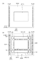
このような固体撮像装置の具体的な平面レイアウトを、図2の固体撮像装置の平面模式図を用いて説明する。図2(A)は第1部材308、即ち第1基板(101)における平面レイアウトを示し、図2(B)は第2部材309、即ち第2基板(121)の平面レイアウトを示している。
A specific planar layout of such a solid-state imaging device will be described with reference to a schematic plan view of the solid-state imaging device in FIG. 2A shows a planar layout of the
図2(A)において、第1部材308には、複数の光電変換素子が配列した画素部301Aと、パッド313が配されたパッド部312A、とが配されている。画素部301Aには、図3における光電変換素子303と転送トランジスタ304と接合部310、311とが複数配されている。また、パッド313と平面的に同一位置に第2部材309との接続のための接合部314Aが配されている。パッド313には外部端子が接続される。パッド313は固体撮像装置に複数配置されており、光電変換素子で生じた電荷に基づく信号(画像信号)を出力するパッドや、外部から供給される周辺回路を駆動するための電圧などが入力されるパッドが含まれる。
2A, the
次に、図2(B)において、第2部材309には、画素部301Bと周辺回路部302とパッド部312Bとが配されている。画素部301Bには画素回路の一部が配されており、図3における増幅トランジスタ306とリセットトランジスタ307と接合部310と接合部311とが複数配置されている。周辺回路部302には周辺回路の一部が配されており、水平走査回路HSR、垂直走査回路VSR、読み出し回路RCとが配されている。パッド部312Bには、第1部材との接続のための接合部314Bと保護ダイオード回路315とが配されている。
Next, in FIG. 2B, the
そして、図2(A)及び図2(B)に示した平面レイアウトを有する第1部材308と第2部材309とが張り合わされて本実施例の固体撮像装置を構成している。具体的には、画素部301Aと画素部301Bとが重なるように配置される。そして、接合部314Aと接合部314Bとが接合し、第1部材の接合部310、接合部311と第2部材の接合部310、接合部311とが接合する。なお、図2では、第2部材309の周辺回路部302Bに対応する第1部材308の領域を周辺回路部302Aで示している。周辺回路部302Aには走査回路の一部、即ち周辺回路の一部を配置してもよい。この接合部の構造については、後に詳述する。
Then, the
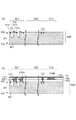
次に、図2及び図3に示した固体撮像装置の断面模式図を図1を用いて説明する。図1では図2、図3と同一の構成には同一の符号を付し、説明を省略する。 Next, a schematic cross-sectional view of the solid-state imaging device shown in FIGS. 2 and 3 will be described with reference to FIG. In FIG. 1, the same components as those in FIGS. 2 and 3 are denoted by the same reference numerals, and description thereof is omitted.
第1部材308は、第1配線構造149と第1基板101とを有する。第1基板101は例えばシリコン半導体基板であり、主面102と裏面103とを有する。第1基板の主面102にはトランジスタが配置されている。第1配線構造149は、層間絶縁膜104、150と、ゲート電極や配線を含むゲート電極層107と、複数の配線を含む配線層109、110と、複数のコンタクトあるいはビアを含むコンタクト層108とを有する。そして、第1配線構造149は第1拡散防止膜111を有する。ここで第1配線構造149に含まれる層間絶縁膜、配線層及びコンタクト層の層数は任意に設定可能である。なお、第1配線構造149の配線層110は、接合部311、314を含み、またコンタクト層と一体となっている。以下、接合部とは電気的な接続を行う第1部材の導電体と第2部材の導電体とが接合している部分であり、接合前の導電体についても接合部と示すものとする。
The
第1部材308の画素部301において、第1基板101には、光電変換素子を構成するn型半導体領域112と、転送トランジスタのドレインであるn型半導体領域114と、素子分離構造119とが配されている。転送トランジスタはn型半導体領域112とn型半導体領域114と、ゲート電極層107に含まれるゲート電極113とで構成される。ここで、n型半導体領域112で蓄積された電荷は、ゲート電極113によって、n型半導体領域114に転送される。n型半導体領域114に転送された電荷に基づく電位はコンタクト層108のコンタクト、配線層109の配線、コンタクト層を含む配線層110を介して、第2部材309へと伝達される。この配線層110に含まれる配線が接合部311を構成する。なお、光電変換素子は更にp型半導体領域を有する埋込みフォトダイオードであってもよく、フォトゲートであってもよく、適宜変更可能である。
In the
画素部301の第1基板101の裏面103側には、平坦化層115、複数のカラーフィルタを含むカラーフィルタ層116、平坦化層117、複数のマイクロレンズを含むマイクロレンズ層118がこの順に配置されている。図1において、複数のカラーフィルタ及び複数のマイクロレンズはそれぞれが1つの光電変換素子に対応して、すなわち画素毎に配置されているが、複数画素に対して1つずつ設けられていてもよい。本実施例の固体撮像装置は、このマイクロレンズ層118側から光が入射し光電変換素子が受光する、所謂、裏面照射型の固体撮像装置である。
On the
第1部材308のパッド部312には、パッド313と、外部端子と接続させるためのパッド313を露出する開口100とが配されている。また、パッド313から入力された電圧を第2部材309に伝達する接合部314Aが配置されている。接合部314Aは画素部の接合部と同様に、配線層110に含まれる。なお、第1部材308において、第2部材309の周辺回路部302に対応する領域には、図1に示したように任意の回路素子120を設けている。
The
第2部材309は、第2配線構造150と第2基板121とを有する。第2基板121は例えばシリコン半導体基板であり、主面122と裏面123とを有する。第2基板の主面122にはトランジスタが配置される。第2配線構造150は、層間絶縁膜124〜127と、ゲート電極や配線を含むゲート電極層128と、複数の配線を含む配線層130、131、132と、複数のコンタクトあるいはビアを含むコンタクト層129とを有する。そして、第2配線構造150は第2拡散防止膜133を有する。ここで第2配線構造150に含まれる層間絶縁膜、配線層及びコンタクト層の層数は任意に設定可能である。なお、第1配線構造150の配線層131及び配線層132は、コンタクト層と一体となっている。そして、配線層132は接合部311、314を含む。
The
第2部材309の画素部301において、第2基板121には、画素回路を構成する増幅トランジスタを構成するウエル135と、増幅トランジスタのソース・ドレイン領域を構成するn型半導体領域138と、素子分離構造136とが配されている。増幅トランジスタは、ウエル135に配され、ゲート電極層128に含まれるゲート電極137と、ソース・ドレイン領域を構成するn型半導体領域138とで構成される。ここで、第1部材308は、接合部311を介して、増幅トランジスタのゲート電極137と接続される。接合部311と増幅トランジスタのゲート電極137とは、配線層132の配線及びビア、配線層131の配線及びビア、配線層130の配線、コンタクト層129のコンタクトとを介して接続される。ここで、図3のノード305は、図1のn型半導体領域114と、配線層109、110、132、131、130の配線及びビアと、コンタクト層108、129のコンタクトと、ゲート電極137と、から構成される。画素部301の他の回路(例えば、リセットトランジスタ)は不図示である。
In the
次に、第2部材309の周辺回路部302には、水平走査回路や垂直走査回路等の制御回路や読み出し回路を含む周辺回路の少なくとも一部が配置されている。図1では、周辺回路に含まれる任意の回路におけるn型のトランジスタとp型のトランジスタを示している。ゲート電極層128に含まれるゲート電極140と、n型のソース・ドレイン領域141とからなるn型トランジスタがp型のウエル139に配置されている。そして、ゲート電極層128に含まれるゲート電極143と、p型のソース・ドレイン領域を構成するp型半導体領域144と、を有するp型トランジスタがn型のウエル142に配置されている。
Next, in the
そして、第2部材309のパッド部312には、第1部材308のパッド313からの信号を入力するための保護ダイオード回路315と、第1部材308と接続するための接合部314Bとが配置されている。接合部314Bは画素部の接合部と同様に、配線層132に含まれる。本実施例の保護ダイオード回路315には、半導体領域から構成される2つのダイオード145、146と、ゲート電極層128からなる2つの抵抗147、148とが含まれている。この保護ダイオード回路315は、一般に使用される保護ダイオード回路が適用可能である。
The
そして、本実施例の固体撮像装置においては、第1基板101の主面102と第2基板121の主面122とが、第1、第2配線構造を介して向かい合う向きに配置されている(対向配置)。つまり、第1基板、第1配線構造、第2配線構造、第2基板の順に配置されている。また、第1配線構造149の上面と、第2配線構造150の上面とが、接合面Xにおいて張り合わされているとも言える。つまり、第1部材308と第2部材309とが接合面Xにて接合されている。接合面Xは、第1配線構造149の上面と第2配線構造150の上面とで構成される。各部材に配置された接合部が接合面Xで接合し、部材間の導通を確保する。そして、外部と信号のやりとりを行うための固体撮像装置のパッド313が第2部材309の主面122の上部に配置され、第1部材308側に開口100が設けられている。
In the solid-state imaging device according to the present embodiment, the
ここで、第1配線構造149において、配線層109はアルミニウムを主成分とする配線(アルミニウム配線)からなり、配線層110は銅を主成分とする配線(銅配線)からなり、デュアルダマシン構造を有する。また、第2配線構造150においては、配線層130は銅配線からなり、シングルダマシン構造を有する。配線層131、132は銅配線からなり、デュアルダマシン構造を有する。配線層110及び配線層132に含まれる配線からなる接合部311及び接合部314(314A及び314B)は、金属接合により接合面Xにおいて接合している。また、パッド部において、外部端子との接続を行うパッド313は、配線層109と同一層、即ち同一高さに配置されており、アルミニウムを主成分とする導電体である。この配線層109、パッド313の高さとは第1基板101の主面102からの高さである。
Here, in the
次に、本実施例の固体撮像装置の製造方法を、図4〜6を用いて説明する。図4は第1部材308の製造工程を示す断面模式図であり、図5は第2部材309の製造工程を示す断面模式図であり、図6は第1部材308と第2部材309とを接合した後の製造工程を示す断面模式図である。
Next, a method for manufacturing the solid-state imaging device according to the present embodiment will be described with reference to FIGS. 4 is a schematic cross-sectional view showing the manufacturing process of the
図1の第1部材308の製造工程を、図4を用いて説明する。図4においては、後に図1の第1部材308になる構成を308’とし、図1の画素部301、周辺回路部302、パッド部312、周辺回路の一部である回路素子120になる部分を304’、302’、312’、120’としている。
A manufacturing process of the
まず、半導体基板を準備し、半導体基板に素子を形成する。主面402と裏面403を有する厚みD3の半導体基板401を用意する。半導体基板401は例えばシリコン半導体基板である。半導体基板401に、素子分離構造119を形成する。素子分離構造119は、シリコン酸化膜などの絶縁体を含み、例えばLOCOSやSTI構造を有する。そして、半導体基板401に任意の導電型のウエル(不図示)を形成する。その後、光電変換素子やトランジスタを構成するn型半導体領域112、114、及びp型半導体領域(不図示)を形成する。また、転送トランジスタのゲート電極113を含むゲート電極を含むゲート電極層107を形成する。ゲート電極層は例えば、ポリシリコン層の堆積及びパターニングによって形成され、ゲート電極のみではなく配線をも含みうる。ここで、ゲート電極、素子分離及び半導体領域の形成方法については、一般的な半導体プロセスで形成可能であり、詳細な説明は省略する。以上によって、図4(A)の構成が得られる。
First, a semiconductor substrate is prepared, and an element is formed on the semiconductor substrate. A
次に、半導体基板401の主面402上に配線構造を形成する。具体的には、まず、ゲート電極層107を覆うように層間絶縁膜104’となる膜を形成する。層間絶縁膜104’となる膜にコンタクトホールを形成し、バリアメタル及びタングステンの膜を形成し、バリアメタル及びタングステンの膜の余分な部分を除去することで層間絶縁膜104’とコンタクト層108を形成する。そして、層間絶縁膜104’上に、バリアメタル及びアルミニウムの膜を成膜し、パターニングすることで配線層109を形成する。次に、配線層109を覆うように層間絶縁膜105となる膜を形成し、第1拡散防止膜106となる膜を形成する。次に、配線110をデュアルダマシン法により形成する。層間絶縁膜105となる膜及び第1拡散防止膜106となる膜の積層膜に、配線用の溝及びビア用の溝(ホール)を形成する。溝を埋めるように拡散防止機能を有するバリアメタルと、銅とを成膜する。余分なバリアメタル及び銅を除去することで配線層110を形成し、層間絶縁膜105及び第1拡散防止膜106が形成される。ここで、第1拡散防止膜106は、配線が露出するような開口を有する。また、第1拡散防止膜106は、バリアメタル及び銅を除去する際に行われるエッチングあるいはCMPによって、同時に平坦化されうる。配線構造の上面は、第1拡散防止膜106の上面及び配線層110の上面により形成される。層間絶縁膜104’は、後に図1の層間絶縁膜104となる。
Next, a wiring structure is formed on the
ここで、層間絶縁膜104’、105はシリコン酸化膜である。しかし層間絶縁膜104’、105はシリコン窒化膜、あるいは有機樹脂等で形成されてもよい。コンタクト108は、例えばタングステンで形成される。配線層110は接合部314A及び311Aを含み、配線層109はパッド313を含む。バリアメタルは導電体である銅に対して拡散防止機能を有し、例えばタンタル、タンタル窒化物等で形成される。第1拡散防止膜106は、接合部を含む配線層110の導電体に対して拡散防止機能を有する膜からなり、例えばシリコン窒化膜やシリコン炭化膜等である。これら配線層、コンタクト層、層間絶縁膜の製造方法については、一般的な半導体プロセスで形成可能であり、詳細な説明は省略する。以上によって、図4(B)の構成が得られる。図4(B)において、符号104’、105、106、108〜110は後に図1における第1配線構造149となる。また、接合部311Aは後に接合部311を構成する。
この図4(B)において、後に図1の接合面Xを構成する第1配線構造149の上面は、第1拡散防止膜106の上面と配線層110の各配線の上面とによって構成されている。この上面の構造については後に詳述する。
Here, the
In FIG. 4B, the upper surface of the
次に、図1の第2部材309の製造工程を、図5を用いて説明する。図5においては、後に図1の第2部材309となる構成を309’とし、図1の画素部301、周辺回路部302、パッド部312、保護ダイオード回路315になる部分を304’、302’、312’、315’としている。
Next, the manufacturing process of the
次に、半導体基板404の主面405上に配線構造を形成する。具体的には、まず、ゲート電極128を覆うように層間絶縁膜124となる膜を成膜する。層間絶縁膜124となる膜にコンタクトホールを形成し、バリアメタル及びタングステンの膜を形成し、バリアメタル及びタングステンの膜の余分な部分を除去することで、層間絶縁膜124とコンタクト層129を形成する。そして、層間絶縁膜124上に層間絶縁膜125となる膜を形成する。次に、配線層130をシングルダマシン法によって形成する。層間絶縁膜125となる膜に配線となる溝を形成し、溝を埋めるように拡散防止機能を有するバリアメタルと、銅とを成膜する。余分なバリアメタル及び銅を除去することで配線層130が形成され、層間絶縁膜125が形成される。次に、層間絶縁膜125及び配線層130を覆うように層間絶縁膜126となる膜を形成する。そして、配線層131をデュアルダマシン法によって形成する。具体的には、層間絶縁膜126となる膜に配線及びビアとなる溝を形成する。溝を埋めるように拡散防止機能を有するバリアメタルと銅とを成膜する。余分なバリアメタル及び銅を除去することで配線層131を形成し、層間絶縁膜126が形成される。そして、層間絶縁膜126及び配線層131を覆うように層間絶縁膜127となる膜及び第2拡散防止膜133となる膜を形成する。次に、配線層132をデュアルダマシン法によって形成する。つまり、層間絶縁膜127及び第2拡散防止膜133となる膜に、配線及びビアとなる溝を形成し、その溝を埋めるように拡散防止機能を有するバリアメタルと銅とを成膜する。拡散防止機能を有するバリアメタルと銅の膜の余分な部分を除去することで配線層132を形成する。この時、バリアメタルは導電体である銅に対して拡散防止機能を有し、例えばタンタル、タンタル窒化物等で形成される。そして、層間絶縁膜127及び第2拡散防止膜133とが形成される。ここで、第2拡散防止膜133は、配線が露出するような開口を有する。また、第2拡散防止膜133は、バリアメタル及び銅を除去する際に行われるエッチングあるいはCMPによって、同時に平坦化されうる。配線構造の上面は、第2拡散防止膜133の上面及び配線層132の上面により形成される。
Next, a wiring structure is formed on the
ここで、層間絶縁膜124〜127はシリコン酸化膜であるが、シリコン窒化膜、あるいは有機樹脂等で形成されてもよい。コンタクト129は、例えばタングステンで形成される。配線層130は銅を主成分とする配線からなり、シングルダマシン構造を有する。配線層131、132は銅を主成分とする配線からなり、デュアルダマシン構造を有する。配線層132は接合部314B及び311Bを含む。これら配線層、コンタクト層、層間絶縁膜の製造方法については、一般的な半導体プロセスで形成可能であり、より詳細な説明は省略する。以上によって、図5(B)の構成が得られる。図5(B)において、符号124〜127、129〜133等は後に図1における第2配線構造150となる。また、接合部311Bは後に接合部311を構成する。
Here, the
この図5(B)において、後に図1の接合面Xを構成する第2配線構造150の上面は、層間絶縁膜127の上面と配線層134の各配線の上面とによって構成されている。配線層134は接合部となる導電体でもある。つまり、第2配線構造150の上面は導電体の上面を含む。この上面の構造については後に詳述する。
In FIG. 5B, the upper surface of the
このような図4(B)及び図5(B)に示した第1部材308’と第2部材309’とを、互いの半導体基板の主面402及び主面405とが向かい合うように張り合わせる。つまり、第1部材308’の配線構造の最上面と第2部材309’の配線構造の最上面とが接合される。ここで、接合部311A、311B及び接合部314A、314Bは銅を主成分とする配線から構成されているため、張り合わせの際は銅の金属接合によって行うことが可能である。なお、張り合わせは、真空あるいは不活性ガスの雰囲気中にて行うことが好ましい。また、張り合わせの前に、各配線構造の上面に対してプラズマ照射を行うことが望ましい。このプラズマ照射を行うことで、プラズマ照射を行わない場合に比べて、シリコン酸化膜やシリコン窒化膜などの層間絶縁膜同士の接合がより強固なものとなる。また、プラズマ照射の他に薬液処理によって活性化する方法も適用可能である。
The
そして、第1部材308’と第2部材309’とが接合された後に、第1部材308’の半導体基板401の裏面403側を薄膜化する。薄膜化は、CMP(化学的機械研磨)やエッチングによって行うことが可能である。そして、半導体基板401は半導体基板407となり、厚みがD3からD1(D1<D3)となる(図6(A))。このように半導体基板401を薄膜化し半導体基板407とすることで、後に入射光が光電変換素子に効率良く入射することを可能にする。また、この時、半導体基板407の厚みD1<半導体基板404の厚みD4となる。
Then, after the
次に、半導体基板407の裏面408に、樹脂からなる平坦化層409、カラーフィルタ層410、樹脂からなる平坦化層411、マイクロレンズ層412をこの順に形成する。これら平坦化層、カラーフィルタ層、マイクロレンズ層の製造方法については、一般的な半導体プロセスで形成可能であり、詳細な説明は省略する。ここでマイクロレンズ層はパッド部となる312’の領域まで形成されていてもよい。以上の工程によって、図6(B)の構成が得られる。
Next, a
そして、パッド313を露出するための開口100を形成する。ここでは、フォトリソグラフィ技術を用いてマイクロレンズ層412の上に任意の開口を有するフォトレジストマスクを設ける。そして、ドライエッチング技術を用いて、マイクロレンズ層421、平坦化層411、カラーフィルタ層410、平坦化層409、半導体基板407及び層間絶縁膜104’を除去し、パッド313を露出させる開口100を形成する。
Then, an
そして、マイクロレンズ層118、平坦化層117、115、カラーフィルタ層116、第1基板101及び層間絶縁膜104が形成される。以上のようにして、図1の構成となる。なお、図6(B)の半導体基板404、主面405、裏面406、厚さD4は、図1の第2基板121、主面122、裏面123、厚さD2と対応している。ここで、厚さD4とD2とは変化がないが、半導体基板404の薄膜化を行い厚さD2<D4となるようにしてもよい。薄膜化によって、工程が増えるが固体撮像装置としての小型化が可能となる。
Then, the
ここで、図7を用いて接合部の詳細について説明を行う。図7は図1の接合部311を拡大して示した断面模式図であり、図7の図1〜6と同一の構成については同一の符号を付し、説明を省略する。 Here, the detail of a junction part is demonstrated using FIG. FIG. 7 is a schematic cross-sectional view showing the joint 311 in FIG. 1 in an enlarged manner. The same components as those in FIGS. 1 to 6 in FIG.
まず、図7(A)は、第1部材及び第2部材の接合前の状態を示し、図7(B)は接合時(図6(A))の状態を示している。第1部材308’には、配線層109と配線層110と第1拡散防止膜111とを有する。配線層109はアルミニウム109aとバリアメタル109bとを含み、配線層110は銅110aとバリアメタル110bとを含む。そして、第2部材309’ には、配線層131と配線層132と第2拡散防止膜133とを有する。配線層131は銅131aとバリアメタル131bを含み、配線層132は銅132aとバリアメタル132bを含む。つまり、接合部は、アルミニウムよりも拡散係数の大きい銅である導電体を含む。ここで、導電体は、銅に限らず、銅を主成分とする合金や、金などの他の金属及び合金であってもよい。ここで、銅のバリアメタルは銅に対して拡散防止能力を有する拡散防止膜である。このバリアメタルとしては、例えば、タンタル、タンタル窒化膜、マンガン、ニオブ、クロム等の金属及びその合金があげられる。そして第1拡散防止膜及び第2拡散防止膜は、例えば、シリコン窒化膜、シリコン炭化膜、シリコン炭窒化膜、シリコン酸窒化膜などがあげられる。そして、銅110aは面X1で露出している部分を除き、バリアメタル110bによって囲まれている。そして、銅132aは面X2で露出している部分を除き、バリアメタル132bによって囲まれている。ここで、面X1は第1配線構造149の上面であり、面X2は第2配線構造150の上面である。
First, FIG. 7A shows a state before joining the first member and the second member, and FIG. 7B shows a state at the time of joining (FIG. 6A). The
図7(B)に示すように、面X1及び面X2とが接合面Xとなり、第1部材308’及び第2部材309’が接合される。銅110a及び銅132aとは金属接合している。ここで、銅110a及び銅132aとは、銅に対する拡散防止機能を有する拡散防止膜であるバリアメタル110b及びバリアメタル132bによって囲まれている。このような構成によれば、接合部において導電体が拡散防止膜によって囲まれているため、暗電流やリーク電流の発生を抑制することが可能な固体撮像装置を提供することが可能となる。
As shown in FIG. 7B, the surface X1 and the surface X2 become the joining surface X, and the first member 308 'and the second member 309' are joined.
ここで、図7(C)は図7(A)の構成において、接合部を構成する配線層110と配線層132との位置がずれていた場合について示した断面模式図である。図7(C)のような場合においても、第1拡散防止膜111及び第2拡散防止膜133とを有することで、接合部において導電体を拡散防止膜によって囲むことが出来る。具体的には、図7(D)に示すように銅110a及び銅132aは、拡散防止膜であるバリアメタル110b及びバリアメタル132bと、第1拡散防止膜111及び第2拡散防止膜133とによって囲まれている。このような構成を有することで、例えプロセスばらつきによって位置がずれた場合においても、接合部において導電体が拡散防止膜によって囲まれているため、暗電流やリーク電流の発生を抑制することが可能な固体撮像装置を提供することが可能となる。
Here, FIG. 7C is a schematic cross-sectional view illustrating a case where the positions of the
本発明は本実施例の製造方法において説明した工程に限定されるものではなく、工程順が変更されていてもよい。また、第1部材308と第2部材309の製造順番については適宜設定可能である。また、半導体基板401、402にはSOI基板を適用することも可能である。なお、第1部材308と第2部材309とを固体撮像装置用の基板として別々に購入し、張り合わせて形成することも可能である。
This invention is not limited to the process demonstrated in the manufacturing method of a present Example, The process order may be changed. The manufacturing order of the
次に、本発明の実施例2について、図8及び図9を用いて説明する。本実施例では接合部の構成に関するいくつかの変形例を説明する。図8は図7に対応した接合部に着目した断面模式図である。図8において図1〜7と同様の構成については同一の符号を付し、説明を省略する。 Next, a second embodiment of the present invention will be described with reference to FIGS. In this embodiment, several modified examples relating to the configuration of the joint will be described. FIG. 8 is a schematic cross-sectional view focusing on the joint corresponding to FIG. In FIG. 8, the same components as those in FIGS.
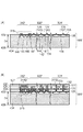
まず、図8(A)及び図8(B)に示す接合部の変形例について説明する。図8(A)は図7(A)に対応する断面模式図であり、図8(B)は図7(B)に対応する断面模式図である。図8(A)において、図7(A)との違いは、配線層110が配線層132よりも小さい面積の露出面を有している点、第2の部材309’が第2拡散防止膜133を有していない点である。図8(A)において示されているのは一部の断面ではあるが、配線層110の面X1における面積は、配線層132の面X2における面積よりも小さい。このような構成においても、接合後の図8(B)に示すように、銅110a及び銅132aは拡散防止膜であるバリアメタル110a及び132aと、第1拡散防止膜111によって囲まれている。
First, a modification of the joint shown in FIGS. 8A and 8B will be described. 8A is a schematic cross-sectional view corresponding to FIG. 7A, and FIG. 8B is a schematic cross-sectional view corresponding to FIG. 7B. 8A differs from FIG. 7A in that the
次に、図8(C)及び図8(D)に示す接合部の変形例について説明する。図8(C)は図8(A)に対応する断面模式図であり、図8(D)は図8(B)に対応する断面模式図である。図8(C)において、図8(A)との違いは、面X1において配線層110の部分が凹部801となっている点である。具体的には、層間絶縁膜105及び配線層110の上部に第1拡散防止膜111が配置されており、第1拡散防止膜111が配線層110に対応した開口を有している。このような構成においても、接合後の図8(D)に示すように、銅110a及び銅132aは拡散防止膜であるバリアメタル110a及び132aと、第1拡散防止膜111によって囲まれている。ここでは、凹部801は第1拡散防止膜111の厚み分の段差を有しているが、例えば銅110aを一部除去して段差を大きくしてもよい。なお、凹部801を有していても、銅などの導電体の熱膨張係数は拡散防止膜や層間絶縁膜を構成する誘電体よりも大きいので、接合の接合面Xは図8(D)のような平らな面を有することが可能である。
Next, a modification of the joint shown in FIGS. 8C and 8D will be described. 8C is a schematic cross-sectional view corresponding to FIG. 8A, and FIG. 8D is a schematic cross-sectional view corresponding to FIG. 8B. 8C is different from FIG. 8A in that a portion of the
次に、図8(E)及び図8(F)に示す接合部の変形例について説明する。図8(E)は図8(C)に対応する断面模式図であり、図8(F)は図8(D)に対応する断面模式図である。図8(E)において、図8(C)との違いは、面X1において配線層110の部分が凸部802となっている点である。具体的には、第1拡散防止膜111等が形成する面X1よりも銅110aが厚みD分だけ凸となっている。このような構成においても、接合後の図8(F)に示すように、銅110a及び銅132aは拡散防止膜であるバリアメタル110a及び132aと、第1拡散防止膜111によって囲まれている。ここでは、凸部801はなだらかな形状を有しているが、矩形の形状であってもよい。なお、凸部802を有していても、接合時に圧力をかけることから、接合後の接合面Xは、図8(F)のような平らな面を有することが可能である。
Next, a modification of the joint shown in FIGS. 8E and 8F will be described. 8E is a schematic cross-sectional view corresponding to FIG. 8C, and FIG. 8F is a schematic cross-sectional view corresponding to FIG. 8D. 8E is different from FIG. 8C in that a portion of the
次に、図8(G)及び図8(H)に示す接合部の変形例について説明する。図8(G)は図8(E)に対応する断面模式図であり、図8(H)は図8(F)に対応する断面模式図である。図8(G)において、図8(E)との違いは、主に3点である。面X2においても配線層132の部分が凸部803となっている点と、配線層110の面X1における面積と配線層132の面X2における面積とが等しい点と、第2部材309’が第2拡散防止膜133を有する点である。銅110aは面X1よりも厚みD1分だけ凸となっており、銅132aは面X2よりも厚みD2分だけ凸となっている。このような構成においても、接合後の図8(H)に示すように、銅110a及び銅132aは拡散防止膜であるバリアメタル110a及び132aと、第1拡散防止膜111及び第2拡散防止膜133によって囲まれている。ここで、第1部材308’と第2部材309’との間に空隙804が形成されている。銅110a及び銅132aは、空隙804と接しているため、この空隙804の界面において銅が拡散する可能性がある。しかしながら、第1拡散防止膜111及び第2拡散防止膜132を有することで、第1部材308’や第2部材309’の基板側への銅の拡散を抑制することが可能となる。当然のことながら、図8(G)の構成を接合した後に、空隙804が形成されない場合もありうる。
Next, a modification of the joint portion illustrated in FIGS. 8G and 8H will be described. FIG. 8G is a schematic cross-sectional view corresponding to FIG. 8E, and FIG. 8H is a schematic cross-sectional view corresponding to FIG. The difference between FIG. 8G and FIG. 8E is mainly three points. Also in the surface X2, the
以上述べたように、図8に示したような構成においても、接合部において銅が拡散防止膜によって囲むことが可能となる。従って、暗電流やリーク電流の発生を抑制することが可能な固体撮像装置を提供することが可能となる。 As described above, even in the configuration as shown in FIG. 8, copper can be surrounded by the diffusion prevention film at the junction. Therefore, it is possible to provide a solid-state imaging device that can suppress the generation of dark current and leakage current.
ここで、図8(E)及び図8(G)に示した凸部を有する接合部について、図8(G)の接合部311Bに着目して形成方法を説明する。まず、層間絶縁膜126、配線層131、層間絶縁膜127を形成する。そして、層間絶縁膜127に、デュアルダマシン法により配線層132を形成する。ここで、余分な銅及びバリアメタルの膜を除去する際に、例えばCMPを用いる場合には研磨速度やスラリーを調整することで、エッチングを用いる場合にはエッチングガス等を調整することで、凸を有する銅132aが形成可能である(図9(A))。次に、凸を覆って第2拡散防止膜となる膜1331を成膜し(図9(B))、エッチングあるいはCMPによって、第2拡散防止膜となる膜1331の一部を除去することで、第2拡散防止膜133及び凸部803が形成可能である(図9(C))。
Here, a method for forming the joint portion having the convex portions illustrated in FIGS. 8E and 8G will be described by focusing on the
なお、図9においては、層間絶縁膜126及び層間絶縁膜127が複数の絶縁膜から構成されており、また、配線層131の上部を覆う拡散防止膜701が配置されている。このように、層間絶縁膜の構成は適宜設定可能である。
In FIG. 9, the
以上、本実施例においては、接合部の構成の変形例を示した。各変形例は適宜組み合わせ可能であり、第1部材及び第2部材の接合部のいずれかに適用するかは適宜設定可能である。 As described above, in the present embodiment, the modification of the configuration of the joint portion has been shown. Each modification can be combined as appropriate, and it can be set as appropriate as to whether the modification is applied to the joint portion of the first member or the second member.
次に、本発明の実施例3について、図10及び図11を用いて説明する。本実施例では接合部の構成に関するいくつかの変形例を説明する。図10は図8にて説明した接合部に関する断面模式図である。図10において図1〜7と同様の構成については同一の符号を付し、説明を省略する。 Next, Embodiment 3 of the present invention will be described with reference to FIGS. In this embodiment, several modified examples relating to the configuration of the joint will be described. FIG. 10 is a schematic cross-sectional view of the joint described in FIG. 10, the same components as those in FIGS. 1 to 7 are denoted by the same reference numerals, and description thereof is omitted.
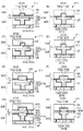
図10(A)及び図10(B)は互いに対応した図面であり、図8(B)あるいは図8(D)の接合部が複数配置された断面模式図を示している。図10(C)は図10(B)の構成の変形例を示している。 10 (A) and 10 (B) are drawings corresponding to each other, and show schematic cross-sectional views in which a plurality of joint portions shown in FIG. 8 (B) or FIG. 8 (D) are arranged. FIG. 10C shows a modified example of the configuration of FIG.
まず、図10(A)において、第1拡散防止膜111は複数の接合部311に共通に設けられている。図10(B)では、第1拡散防止膜111Pは接合部の周囲を囲うようにパターニングされており、各接合部311の間の第1拡散防止膜111は除去されている。また、図10(C)は図10(B)に比べて更に第2拡散防止膜133Pを有し、第2拡散防止膜133Pは第1拡散防止膜111Pと同様に接合部の周囲を囲うようにパターニングされている。
First, in FIG. 10A, the first
ここで、第1拡散防止膜はシリコン窒化膜からなり、層間絶縁膜はシリコン酸化物からなるため、第1拡散防止膜の方が層間絶縁膜よりも誘電率が高い。このような誘電率が高い膜を配線の周りに配置すると配線の寄生容量が増大してしまう。よって、図10(B)の構成にすることによって、図10(A)の構成に比べて、配線間の寄生容量を低減することが可能となる。また、図10(C)のように第2拡散防止膜133Pを有する場合においても寄生容量を低減可能である。なお、拡散防止膜701についても、図10(B)及び図10(C)に示すようにパターニングしてもよい。
Here, since the first diffusion preventing film is made of a silicon nitride film and the interlayer insulating film is made of silicon oxide, the first diffusion preventing film has a dielectric constant higher than that of the interlayer insulating film. If such a film having a high dielectric constant is disposed around the wiring, the parasitic capacitance of the wiring increases. Therefore, with the structure in FIG. 10B, the parasitic capacitance between wirings can be reduced as compared with the structure in FIG. Further, the parasitic capacitance can be reduced even when the second
図11は、接合部311における配線層110と、配線層132と、第1拡散防止膜と、第2拡散防止膜の位置関係を説明するために各構成の外縁を平面に示した平面模式図である。言い換えると接合面Xにおける各構成の配置ともいえる。図11において図1〜10と同様の構成については同一の符号を付し、説明を省略する。
FIG. 11 is a schematic plan view showing the outer edge of each component in a plane in order to explain the positional relationship among the
図11(A)は、図10(B)に対応した平面模式図である。図11(A)のAB線が図10(B)の断面と対応する。図11(A)に示すように、第1拡散防止膜111Pが最も面積が大きく、配線層132を覆っている。つまり、配線層132の銅が露出した面は、第1拡散防止膜111Pと配線層110に対応する。このようなパターンの大小関係を有することで銅を拡散防止膜で覆うことが容易となる。
FIG. 11A is a schematic plan view corresponding to FIG. The line AB in FIG. 11A corresponds to the cross section in FIG. As shown in FIG. 11A, the first
図11(B)及び図11(C)は、図10(C)に対応した平面模式図である。図11(B)及び図11(C)のCD線が図10(C)の断面と対応する。図11(B)においては、配線層110、配線層132、第1拡散防止膜111P、第2拡散防止膜133Pがこの順に大きな面積を有している。このようなパターンの大小関係を有することで、配線層132の銅が露出した面は、第1拡散防止膜111Pと配線層110に対応し、銅を拡散防止膜で覆うことが可能となる。
11 (B) and 11 (C) are schematic plan views corresponding to FIG. 10 (C). The CD line in FIGS. 11B and 11C corresponds to the cross section in FIG. In FIG. 11B, the
図11(C)は、図11(B)とは配線層110、配線層132のパターンが異なる。配線層110と配線層132は、第1方向と、それと異なる第2方向にそれぞれ長辺を有するパターンとなっている。このようなパターンを有することで、接合時の位置ずれの許容範囲を拡大することが可能となる。
FIG. 11C is different from FIG. 11B in the pattern of the
本実施例のように、第1拡散防止膜、第2拡散防止膜、接合部の形状は任意の形状が可能であり、適宜選択可能である。 As in this embodiment, the shapes of the first diffusion preventing film, the second diffusion preventing film, and the bonding portion can be any shape and can be appropriately selected.
以下、上記の各実施例に係る固体撮像装置の応用例として、固体撮像装置が組み込まれた撮像システムについて例示的に説明する。撮像システムには、撮影を主目的とするカメラなどの装置のみならず、撮影機能を補助的に備える装置(例えば、パーソナルコンピュータ、携帯端末)も含まれる。例えば、カメラは、本発明に係る固体撮像装置と、固体撮像装置から出力される信号を処理する処理部とを含む。この処理部とは、例えば、A/D変換器、及びA/D変換器から出力されるデジタルデータを処理するプロセッサを含みうる。 Hereinafter, as an application example of the solid-state imaging device according to each of the above embodiments, an imaging system in which the solid-state imaging device is incorporated will be exemplarily described. The imaging system includes not only a device such as a camera whose main purpose is photographing but also a device (for example, a personal computer or a portable terminal) that is supplementarily provided with a photographing function. For example, the camera includes a solid-state imaging device according to the present invention and a processing unit that processes a signal output from the solid-state imaging device. The processing unit may include, for example, an A / D converter and a processor that processes digital data output from the A / D converter.
以上述べてきたように、本発明の固体撮像装置によれば、暗電流やリーク電流の発生を抑制することが可能な固体撮像装置を提供することが可能となる。 As described above, according to the solid-state imaging device of the present invention, it is possible to provide a solid-state imaging device capable of suppressing the generation of dark current and leakage current.
なお、本発明は明細書記載の構成に限定されるものではなく、画素回路が変更され、第1部材には光電変換素子のみが配置されている場合であってもよい。また、導電型や回路を逆導電型にした構成や、配線層や層間絶縁膜を更に設ける構成や、シングルダマシン構造からデュアルダマシン構造にする場合など適宜変更可能である。また、各実施例の構成を適宜組み合わせることも可能である。 Note that the present invention is not limited to the configuration described in the specification, and may be a case where the pixel circuit is changed and only the photoelectric conversion element is arranged on the first member. In addition, the structure can be changed as appropriate, such as a structure in which the conductivity type or the circuit is reversed, a structure in which a wiring layer or an interlayer insulating film is further provided, or a single damascene structure to a dual damascene structure. Moreover, it is also possible to combine the structure of each Example suitably.
また、本発明は固体撮像装置に限られるものではなく、DRAM等の一般半導体装置にも適用可能である。 Further, the present invention is not limited to a solid-state imaging device, but can be applied to a general semiconductor device such as a DRAM.
301 画素部
302 周辺回路部
308 第1部材
309 第2部材
149 第1配線構造
150 第2配線構造
311 接合部
314 接合部
101 第1基板
121 第2基板
X 接合面
111 第1拡散防止膜
133 第2拡散防止膜
301
Claims (13)
前記第1基板の主面の上に配され、導電体を含む第1の接合部を有する第1配線構造と、
前記光電変換素子の電荷に基づく信号を読み出すための読み出し回路および制御回路を含む周辺回路の一部が主面に配された第2基板と、
前記第2基板の主面の上に配され、導電体を含む第2の接合部を有する第2配線構造と、を有し、
前記第1基板と、前記第1配線構造と、前記第2配線構造と、前記第2基板とがこの順に配置されるように前記第1の接合部及び前記第2の接合部とが接合された固体撮像装置において、
前記第1の接合部の導電体と、前記第2の接合部の導電体とは、前記導電体に対する拡散防止膜で囲まれており、
前記拡散防止膜は更に第1拡散防止膜を有し、
前記第1配線構造の上面は、前記第1の接合部と、前記第1拡散防止膜とで構成されていることを特徴とする固体撮像装置。 A first substrate on which a photoelectric conversion element is arranged on a main surface;
A first wiring structure disposed on a main surface of the first substrate and having a first joint including a conductor;
A second substrate in which a part of a peripheral circuit including a reading circuit and a control circuit for reading a signal based on a charge of the photoelectric conversion element is arranged on a main surface;
A second wiring structure that is disposed on the main surface of the second substrate and has a second joint including a conductor;
The first bonding portion and the second bonding portion are bonded so that the first substrate, the first wiring structure, the second wiring structure, and the second substrate are arranged in this order. In the solid-state imaging device
The conductor of the first joint and the conductor of the second joint are surrounded by a diffusion prevention film for the conductor ,
The diffusion prevention film further includes a first diffusion prevention film,
The solid-state imaging device according to claim 1, wherein an upper surface of the first wiring structure includes the first bonding portion and the first diffusion prevention film .
前記第2の接合部は、前記導電体と、バリアメタルを有し、
前記導電体に対する拡散防止膜は前記バリアメタルであることを特徴とする請求項1に記載の固体撮像装置。 The first joint has the conductor and a barrier metal,
The second joint portion includes the conductor and a barrier metal,
The solid-state imaging device according to claim 1, wherein the diffusion prevention film for the conductor is the barrier metal.
前記第1の接合部のバリアメタルは、前記第1の接合部の導電体と前記層間絶縁膜との間に配置されていることを特徴とする請求項2に記載の固体撮像装置。 The first wiring structure has an interlayer insulating film in which the first junction is disposed,
3. The solid-state imaging device according to claim 2, wherein the barrier metal of the first joint is disposed between the conductor of the first joint and the interlayer insulating film.
前記第2の接合部のバリアメタルは、前記第2の接合部の導電体と前記層間絶縁膜との間に配置されていることを特徴とする請求項2または3に記載の固体撮像装置。 The second wiring structure includes an interlayer insulating film in which the second bonding portion is disposed,
The barrier metal of the second junction, the solid-state imaging device according to claim 2 or 3, characterized in that it is disposed between the conductors of the second joint portion and the interlayer insulating film.
前記第2配線構造の上面は、前記第2の接合部と、前記第2拡散防止膜とで構成されていることを特徴とする請求項1乃至8のいずれか1項に記載の固体撮像装置。 The diffusion prevention film further has a second diffusion prevention film,
The upper surface of the second wiring structure, the second joint portion, the solid-state imaging device according to any one of claims 1 to 8, characterized in that it is constituted by a second diffusion barrier layer .
前記固体撮像装置からの信号を処理する信号処理回路とを有する撮像システム。 A solid-state imaging device according to any one of claims 1 to 12 ,
An imaging system having a signal processing circuit for processing a signal from the solid-state imaging device.
Priority Applications (16)
| Application Number | Priority Date | Filing Date | Title |
|---|---|---|---|
| JP2010156926A JP5451547B2 (en) | 2010-07-09 | 2010-07-09 | Solid-state imaging device |
| EP11803305.9A EP2591505A4 (en) | 2010-07-09 | 2011-07-04 | Solid-state image pickup device |
| RU2013105505/28A RU2521224C1 (en) | 2010-07-09 | 2011-07-04 | Image acquisition solid-state device |
| PCT/JP2011/003796 WO2012004965A1 (en) | 2010-07-09 | 2011-07-04 | Solid-state image pickup device |
| CN201180033415.3A CN102971851B (en) | 2010-07-09 | 2011-07-04 | Solid-state image pickup apparatus |
| EP20166179.0A EP3706172A1 (en) | 2010-07-09 | 2011-07-04 | Solid-state image pickup device |
| CN201610164142.0A CN105720067B9 (en) | 2010-07-09 | 2011-07-04 | Solid-state image pickup apparatus |
| US13/808,877 US9166090B2 (en) | 2010-07-09 | 2011-07-04 | Solid-state image pickup device |
| US14/856,354 US9419030B2 (en) | 2010-07-09 | 2015-09-16 | Solid-state image pickup device |
| US15/209,605 US9640581B2 (en) | 2010-07-09 | 2016-07-13 | Solid-state image pickup device |
| US15/456,386 US9929202B2 (en) | 2010-07-09 | 2017-03-10 | Solid-state image pickup device |
| US15/894,258 US10217786B2 (en) | 2010-07-09 | 2018-02-12 | Solid-state image pickup device |
| US16/242,835 US10573680B2 (en) | 2010-07-09 | 2019-01-08 | Solid-state image pickup device |
| US16/777,586 US11177310B2 (en) | 2010-07-09 | 2020-01-30 | Solid-state image pickup device |
| US17/505,039 US20220037390A1 (en) | 2010-07-09 | 2021-10-19 | Solid-state image pickup device |
| US18/322,239 US20230299112A1 (en) | 2010-07-09 | 2023-05-23 | Solid-state image pickup device |
Applications Claiming Priority (1)
| Application Number | Priority Date | Filing Date | Title |
|---|---|---|---|
| JP2010156926A JP5451547B2 (en) | 2010-07-09 | 2010-07-09 | Solid-state imaging device |
Publications (3)
| Publication Number | Publication Date |
|---|---|
| JP2012019147A JP2012019147A (en) | 2012-01-26 |
| JP2012019147A5 JP2012019147A5 (en) | 2013-08-22 |
| JP5451547B2 true JP5451547B2 (en) | 2014-03-26 |
Family
ID=45440958
Family Applications (1)
| Application Number | Title | Priority Date | Filing Date |
|---|---|---|---|
| JP2010156926A Active JP5451547B2 (en) | 2010-07-09 | 2010-07-09 | Solid-state imaging device |
Country Status (6)
| Country | Link |
|---|---|
| US (9) | US9166090B2 (en) |
| EP (2) | EP2591505A4 (en) |
| JP (1) | JP5451547B2 (en) |
| CN (2) | CN105720067B9 (en) |
| RU (1) | RU2521224C1 (en) |
| WO (1) | WO2012004965A1 (en) |
Families Citing this family (45)
| Publication number | Priority date | Publication date | Assignee | Title |
|---|---|---|---|---|
| CN102668081B (en) | 2009-12-26 | 2016-02-03 | 佳能株式会社 | Solid-state image pickup apparatus and image picking system |
| JP5451547B2 (en) * | 2010-07-09 | 2014-03-26 | キヤノン株式会社 | Solid-state imaging device |
| US8896125B2 (en) | 2011-07-05 | 2014-11-25 | Sony Corporation | Semiconductor device, fabrication method for a semiconductor device and electronic apparatus |
| TWI495041B (en) * | 2011-07-05 | 2015-08-01 | Sony Corp | Semiconductor device, fabrication method for a semiconductor device and electronic apparatus |
| JP5994274B2 (en) * | 2012-02-14 | 2016-09-21 | ソニー株式会社 | SEMICONDUCTOR DEVICE, SEMICONDUCTOR DEVICE MANUFACTURING METHOD, AND ELECTRONIC DEVICE |
| US10090349B2 (en) | 2012-08-09 | 2018-10-02 | Taiwan Semiconductor Manufacturing Company, Ltd. | CMOS image sensor chips with stacked scheme and methods for forming the same |
| US9153565B2 (en) | 2012-06-01 | 2015-10-06 | Taiwan Semiconductor Manufacturing Company, Ltd. | Image sensors with a high fill-factor |
| KR101240537B1 (en) * | 2012-05-07 | 2013-03-11 | (주)실리콘화일 | Manufacture method for image sensor having 3 dimension structure |
| JP6012262B2 (en) | 2012-05-31 | 2016-10-25 | キヤノン株式会社 | Manufacturing method of semiconductor device |
| US8796805B2 (en) * | 2012-09-05 | 2014-08-05 | Taiwan Semiconductor Manufacturing Company, Ltd. | Multiple metal film stack in BSI chips |
| US8866250B2 (en) * | 2012-09-05 | 2014-10-21 | Taiwan Semiconductor Manufacturing Company, Ltd. | Multiple metal film stack in BSI chips |
| TWI595637B (en) * | 2012-09-28 | 2017-08-11 | Sony Corp | Semiconductor devices and electronic devices |
| JP6128787B2 (en) * | 2012-09-28 | 2017-05-17 | キヤノン株式会社 | Semiconductor device |
| JP6017297B2 (en) * | 2012-12-14 | 2016-10-26 | オリンパス株式会社 | Manufacturing method of semiconductor device |
| KR102136845B1 (en) | 2013-09-16 | 2020-07-23 | 삼성전자 주식회사 | Stack type image sensor and fabrication method thereof |
| JP6212720B2 (en) * | 2013-09-20 | 2017-10-18 | パナソニックIpマネジメント株式会社 | Semiconductor device and manufacturing method thereof |
| TWI676279B (en) * | 2013-10-04 | 2019-11-01 | 新力股份有限公司 | Semiconductor device and solid-state imaging device |
| CN104810366B (en) * | 2014-01-26 | 2018-09-11 | 中芯国际集成电路制造(上海)有限公司 | A kind of integrated circuit and its manufacturing method |
| CN104241201B (en) * | 2014-08-28 | 2017-05-31 | 武汉新芯集成电路制造有限公司 | A kind of method of integrated power device and control device |
| CN104241200B (en) * | 2014-08-28 | 2017-03-08 | 武汉新芯集成电路制造有限公司 | A kind of power device and the integrated approach of control device |
| US10285088B2 (en) * | 2014-09-26 | 2019-05-07 | Nokia Technologies Oy | Methods and apparatus for minimization of drive testing |
| CN104599988B (en) * | 2015-01-05 | 2017-08-04 | 武汉新芯集成电路制造有限公司 | The method of integrated power device and control device |
| US10431614B2 (en) * | 2017-02-01 | 2019-10-01 | Semiconductor Components Industries, Llc | Edge seals for semiconductor packages |
| JP2018195656A (en) | 2017-05-16 | 2018-12-06 | ソニーセミコンダクタソリューションズ株式会社 | Semiconductor device manufacturing method and semiconductor device |
| US20200144322A1 (en) * | 2017-07-18 | 2020-05-07 | Sony Semiconductor Solutions Corporation | Imaging apparatus and method of manufacturing imaging apparatus |
| FR3069371B1 (en) * | 2017-07-19 | 2019-08-30 | Stmicroelectronics (Crolles 2) Sas | ELECTRONIC DEVICE IMAGE SENSOR |
| US10727217B2 (en) | 2017-09-29 | 2020-07-28 | Taiwan Semiconductor Manufacturing Company, Ltd. | Method of manufacturing semiconductor device that uses bonding layer to join semiconductor substrates together |
| US10879115B2 (en) * | 2017-11-21 | 2020-12-29 | Taiwan Semiconductor Manufacturing Co., Ltd. | Semiconductor device and forming method thereof |
| KR102491881B1 (en) * | 2018-01-16 | 2023-01-27 | 삼성디스플레이 주식회사 | Display apparatus |
| WO2019150981A1 (en) * | 2018-02-01 | 2019-08-08 | ソニーセミコンダクタソリューションズ株式会社 | Solid-state imaging device and method for manufacturing same, and electronic apparatus |
| JP2019140178A (en) * | 2018-02-07 | 2019-08-22 | 東芝メモリ株式会社 | Semiconductor device |
| JP7353729B2 (en) * | 2018-02-09 | 2023-10-02 | キヤノン株式会社 | Semiconductor devices and semiconductor device manufacturing methods |
| JP6952629B2 (en) * | 2018-03-20 | 2021-10-20 | 株式会社東芝 | Semiconductor device |
| JP2020043298A (en) * | 2018-09-13 | 2020-03-19 | キヤノン株式会社 | Semiconductor device, manufacturing method thereof, and electronic equipment |
| KR102524998B1 (en) * | 2018-09-13 | 2023-04-24 | 주식회사 디비하이텍 | Backside illuminated image sensor and method of manufacturing the same |
| JP2020123697A (en) * | 2019-01-31 | 2020-08-13 | キヤノン株式会社 | Semiconductor device, semiconductor wafer, apparatus, and manufacturing method |
| US10840185B2 (en) * | 2019-03-05 | 2020-11-17 | Texas Instruments Incorporated | Semiconductor device with vias having a zinc-second metal-copper composite layer |
| JP7321724B2 (en) | 2019-03-05 | 2023-08-07 | キヤノン株式会社 | Semiconductor equipment and equipment |
| JP7297516B2 (en) * | 2019-04-25 | 2023-06-26 | キヤノン株式会社 | Semiconductor equipment and equipment |
| JP2021034560A (en) * | 2019-08-23 | 2021-03-01 | キオクシア株式会社 | Semiconductor device and method for manufacturing the same |
| KR20210025156A (en) | 2019-08-26 | 2021-03-09 | 삼성전자주식회사 | Semiconductor device and method of manufacturing the same |
| JP7417393B2 (en) * | 2019-09-27 | 2024-01-18 | キヤノン株式会社 | Semiconductor devices and semiconductor wafers |
| JP7353121B2 (en) | 2019-10-08 | 2023-09-29 | キヤノン株式会社 | Semiconductor devices and equipment |
| JP2022018705A (en) | 2020-07-16 | 2022-01-27 | キヤノン株式会社 | Semiconductor device |
| KR20220010947A (en) * | 2020-07-20 | 2022-01-27 | 에스케이하이닉스 주식회사 | Image sensing device having protection device |
Family Cites Families (18)
| Publication number | Priority date | Publication date | Assignee | Title |
|---|---|---|---|---|
| US6168965B1 (en) * | 1999-08-12 | 2001-01-02 | Tower Semiconductor Ltd. | Method for making backside illuminated image sensor |
| US6455425B1 (en) * | 2000-01-18 | 2002-09-24 | Advanced Micro Devices, Inc. | Selective deposition process for passivating top interface of damascene-type Cu interconnect lines |
| US6642081B1 (en) * | 2002-04-11 | 2003-11-04 | Robert Patti | Interlocking conductor method for bonding wafers to produce stacked integrated circuits |
| JP4432502B2 (en) * | 2004-01-20 | 2010-03-17 | ソニー株式会社 | Semiconductor device |
| KR100610481B1 (en) | 2004-12-30 | 2006-08-08 | 매그나칩 반도체 유한회사 | Image sensor with enlarged photo detecting area and method for fabrication thereof |
| KR100782463B1 (en) | 2005-04-13 | 2007-12-05 | (주)실리콘화일 | Separation type unit pixel of image sensor having 3 dimension structure and manufacture method thereof |
| JP4533367B2 (en) * | 2005-11-18 | 2010-09-01 | キヤノン株式会社 | Solid-state imaging device |
| JP5162869B2 (en) * | 2006-09-20 | 2013-03-13 | 富士通セミコンダクター株式会社 | Semiconductor device and manufacturing method thereof |
| JP2008277511A (en) * | 2007-04-27 | 2008-11-13 | Fujifilm Corp | Image pickup device and imaging apparatus |
| US7960768B2 (en) | 2008-01-17 | 2011-06-14 | Aptina Imaging Corporation | 3D backside illuminated image sensor with multiplexed pixel structure |
| JP2010067844A (en) * | 2008-09-11 | 2010-03-25 | Omron Corp | Method of manufacturing solid-state image pickup element |
| JP2010156926A (en) | 2009-01-05 | 2010-07-15 | Sharp Corp | Display device and television receiving device |
| JP5187284B2 (en) | 2009-06-26 | 2013-04-24 | ソニー株式会社 | Manufacturing method of semiconductor device |
| CN102668081B (en) * | 2009-12-26 | 2016-02-03 | 佳能株式会社 | Solid-state image pickup apparatus and image picking system |
| JP5451547B2 (en) * | 2010-07-09 | 2014-03-26 | キヤノン株式会社 | Solid-state imaging device |
| US9153490B2 (en) * | 2011-07-19 | 2015-10-06 | Sony Corporation | Solid-state imaging device, manufacturing method of solid-state imaging device, manufacturing method of semiconductor device, semiconductor device, and electronic device |
| TWI577001B (en) * | 2011-10-04 | 2017-04-01 | Sony Corp | Solid-state imaging device, method of manufacturing solid-state imaging device, and electronic device |
| JP2014203961A (en) * | 2013-04-04 | 2014-10-27 | ソニー株式会社 | Solid state image pickup device, process of manufacturing the same, and electronic apparatus |
-
2010
- 2010-07-09 JP JP2010156926A patent/JP5451547B2/en active Active
-
2011
- 2011-07-04 EP EP11803305.9A patent/EP2591505A4/en not_active Withdrawn
- 2011-07-04 CN CN201610164142.0A patent/CN105720067B9/en active Active
- 2011-07-04 RU RU2013105505/28A patent/RU2521224C1/en active
- 2011-07-04 CN CN201180033415.3A patent/CN102971851B/en active Active
- 2011-07-04 WO PCT/JP2011/003796 patent/WO2012004965A1/en active Application Filing
- 2011-07-04 US US13/808,877 patent/US9166090B2/en active Active
- 2011-07-04 EP EP20166179.0A patent/EP3706172A1/en active Pending
-
2015
- 2015-09-16 US US14/856,354 patent/US9419030B2/en active Active
-
2016
- 2016-07-13 US US15/209,605 patent/US9640581B2/en active Active
-
2017
- 2017-03-10 US US15/456,386 patent/US9929202B2/en not_active Expired - Fee Related
-
2018
- 2018-02-12 US US15/894,258 patent/US10217786B2/en not_active Expired - Fee Related
-
2019
- 2019-01-08 US US16/242,835 patent/US10573680B2/en active Active
-
2020
- 2020-01-30 US US16/777,586 patent/US11177310B2/en active Active
-
2021
- 2021-10-19 US US17/505,039 patent/US20220037390A1/en not_active Abandoned
-
2023
- 2023-05-23 US US18/322,239 patent/US20230299112A1/en active Pending
Also Published As
| Publication number | Publication date |
|---|---|
| US20190148446A1 (en) | 2019-05-16 |
| US10217786B2 (en) | 2019-02-26 |
| RU2521224C1 (en) | 2014-06-27 |
| US9166090B2 (en) | 2015-10-20 |
| US9640581B2 (en) | 2017-05-02 |
| US20200168654A1 (en) | 2020-05-28 |
| US10573680B2 (en) | 2020-02-25 |
| CN102971851B (en) | 2016-04-06 |
| CN102971851A (en) | 2013-03-13 |
| EP2591505A1 (en) | 2013-05-15 |
| US20220037390A1 (en) | 2022-02-03 |
| US20230299112A1 (en) | 2023-09-21 |
| JP2012019147A (en) | 2012-01-26 |
| US20180166494A1 (en) | 2018-06-14 |
| CN105720067A (en) | 2016-06-29 |
| WO2012004965A1 (en) | 2012-01-12 |
| US20160005776A1 (en) | 2016-01-07 |
| US9929202B2 (en) | 2018-03-27 |
| CN105720067B9 (en) | 2019-11-19 |
| CN105720067B (en) | 2019-10-01 |
| EP2591505A4 (en) | 2014-04-16 |
| US11177310B2 (en) | 2021-11-16 |
| US9419030B2 (en) | 2016-08-16 |
| US20170186803A1 (en) | 2017-06-29 |
| EP3706172A1 (en) | 2020-09-09 |
| US20130112849A1 (en) | 2013-05-09 |
| US20160322415A1 (en) | 2016-11-03 |
Similar Documents
| Publication | Publication Date | Title |
|---|---|---|
| JP5451547B2 (en) | Solid-state imaging device | |
| JP5517800B2 (en) | Member for solid-state imaging device and method for manufacturing solid-state imaging device | |
| JP5553693B2 (en) | Solid-state imaging device and imaging system | |
| JP5693060B2 (en) | Solid-state imaging device and imaging system | |
| JP5843475B2 (en) | Solid-state imaging device and method for manufacturing solid-state imaging device | |
| JP2012033894A (en) | Solid state image sensor | |
| JP7309670B2 (en) | Solid-state imaging device | |
| JP2023055816A (en) | Solid state image pickup device and solid state image pickup device manufacturing method |
Legal Events
| Date | Code | Title | Description |
|---|---|---|---|
| A521 | Request for written amendment filed |
Free format text: JAPANESE INTERMEDIATE CODE: A523 Effective date: 20130709 |
|
| A621 | Written request for application examination |
Free format text: JAPANESE INTERMEDIATE CODE: A621 Effective date: 20130709 |
|
| TRDD | Decision of grant or rejection written | ||
| A01 | Written decision to grant a patent or to grant a registration (utility model) |
Free format text: JAPANESE INTERMEDIATE CODE: A01 Effective date: 20131203 |
|
| A61 | First payment of annual fees (during grant procedure) |
Free format text: JAPANESE INTERMEDIATE CODE: A61 Effective date: 20131226 |
|
| R151 | Written notification of patent or utility model registration |
Ref document number: 5451547 Country of ref document: JP Free format text: JAPANESE INTERMEDIATE CODE: R151 |