WO2012004965A1 - Solid-state image pickup device - Google Patents
Solid-state image pickup device Download PDFInfo
- Publication number
- WO2012004965A1 WO2012004965A1 PCT/JP2011/003796 JP2011003796W WO2012004965A1 WO 2012004965 A1 WO2012004965 A1 WO 2012004965A1 JP 2011003796 W JP2011003796 W JP 2011003796W WO 2012004965 A1 WO2012004965 A1 WO 2012004965A1
- Authority
- WO
- WIPO (PCT)
- Prior art keywords
- bonding portion
- image pickup
- solid
- pickup device
- state image
- Prior art date
Links
- 238000009792 diffusion process Methods 0.000 claims abstract description 108
- 239000000758 substrate Substances 0.000 claims abstract description 90
- 239000004020 conductor Substances 0.000 claims abstract description 42
- 230000002093 peripheral effect Effects 0.000 claims abstract description 32
- 239000010949 copper Substances 0.000 claims description 69
- 229910052802 copper Inorganic materials 0.000 claims description 69
- RYGMFSIKBFXOCR-UHFFFAOYSA-N Copper Chemical compound [Cu] RYGMFSIKBFXOCR-UHFFFAOYSA-N 0.000 claims description 67
- 239000011229 interlayer Substances 0.000 claims description 56
- 229910052751 metal Inorganic materials 0.000 claims description 48
- 239000002184 metal Substances 0.000 claims description 48
- 230000004888 barrier function Effects 0.000 claims description 41
- 230000003321 amplification Effects 0.000 claims description 14
- 238000003199 nucleic acid amplification method Methods 0.000 claims description 14
- 229910052581 Si3N4 Inorganic materials 0.000 claims description 8
- HQVNEWCFYHHQES-UHFFFAOYSA-N silicon nitride Chemical compound N12[Si]34N5[Si]62N3[Si]51N64 HQVNEWCFYHHQES-UHFFFAOYSA-N 0.000 claims description 8
- 229910052782 aluminium Inorganic materials 0.000 claims description 7
- XAGFODPZIPBFFR-UHFFFAOYSA-N aluminium Chemical compound [Al] XAGFODPZIPBFFR-UHFFFAOYSA-N 0.000 claims description 7
- 150000002739 metals Chemical class 0.000 claims description 7
- 229910045601 alloy Inorganic materials 0.000 claims description 5
- 239000000956 alloy Substances 0.000 claims description 5
- HBMJWWWQQXIZIP-UHFFFAOYSA-N silicon carbide Chemical compound [Si+]#[C-] HBMJWWWQQXIZIP-UHFFFAOYSA-N 0.000 claims description 4
- 229910010271 silicon carbide Inorganic materials 0.000 claims description 4
- 238000003384 imaging method Methods 0.000 claims 1
- 239000010410 layer Substances 0.000 description 136
- 239000004065 semiconductor Substances 0.000 description 47
- 238000000034 method Methods 0.000 description 35
- 238000004519 manufacturing process Methods 0.000 description 20
- 230000009977 dual effect Effects 0.000 description 11
- 230000004048 modification Effects 0.000 description 11
- 238000012986 modification Methods 0.000 description 11
- 238000005530 etching Methods 0.000 description 6
- 230000008569 process Effects 0.000 description 6
- 230000001681 protective effect Effects 0.000 description 6
- VYPSYNLAJGMNEJ-UHFFFAOYSA-N Silicium dioxide Chemical compound O=[Si]=O VYPSYNLAJGMNEJ-UHFFFAOYSA-N 0.000 description 5
- XUIMIQQOPSSXEZ-UHFFFAOYSA-N Silicon Chemical compound [Si] XUIMIQQOPSSXEZ-UHFFFAOYSA-N 0.000 description 5
- 239000000470 constituent Substances 0.000 description 5
- 238000002955 isolation Methods 0.000 description 5
- 229910052710 silicon Inorganic materials 0.000 description 5
- 239000010703 silicon Substances 0.000 description 5
- 229910052814 silicon oxide Inorganic materials 0.000 description 5
- WFKWXMTUELFFGS-UHFFFAOYSA-N tungsten Chemical compound [W] WFKWXMTUELFFGS-UHFFFAOYSA-N 0.000 description 5
- 239000010937 tungsten Substances 0.000 description 5
- 229910052721 tungsten Inorganic materials 0.000 description 5
- 238000000059 patterning Methods 0.000 description 4
- 239000011347 resin Substances 0.000 description 4
- 229920005989 resin Polymers 0.000 description 4
- 230000003071 parasitic effect Effects 0.000 description 3
- 229910052715 tantalum Inorganic materials 0.000 description 3
- GUVRBAGPIYLISA-UHFFFAOYSA-N tantalum atom Chemical compound [Ta] GUVRBAGPIYLISA-UHFFFAOYSA-N 0.000 description 3
- MZLGASXMSKOWSE-UHFFFAOYSA-N tantalum nitride Chemical compound [Ta]#N MZLGASXMSKOWSE-UHFFFAOYSA-N 0.000 description 3
- 230000003247 decreasing effect Effects 0.000 description 2
- 239000012535 impurity Substances 0.000 description 2
- 238000005498 polishing Methods 0.000 description 2
- 230000009467 reduction Effects 0.000 description 2
- 230000035945 sensitivity Effects 0.000 description 2
- 239000000126 substance Substances 0.000 description 2
- VYZAMTAEIAYCRO-UHFFFAOYSA-N Chromium Chemical compound [Cr] VYZAMTAEIAYCRO-UHFFFAOYSA-N 0.000 description 1
- 230000004913 activation Effects 0.000 description 1
- 230000008901 benefit Effects 0.000 description 1
- 230000015572 biosynthetic process Effects 0.000 description 1
- 238000006243 chemical reaction Methods 0.000 description 1
- 229910052804 chromium Inorganic materials 0.000 description 1
- 239000011651 chromium Substances 0.000 description 1
- 238000011109 contamination Methods 0.000 description 1
- 230000008021 deposition Effects 0.000 description 1
- 238000010586 diagram Methods 0.000 description 1
- 239000003989 dielectric material Substances 0.000 description 1
- 238000001312 dry etching Methods 0.000 description 1
- -1 for example Substances 0.000 description 1
- 239000007789 gas Substances 0.000 description 1
- 239000011261 inert gas Substances 0.000 description 1
- 239000011810 insulating material Substances 0.000 description 1
- WPBNNNQJVZRUHP-UHFFFAOYSA-L manganese(2+);methyl n-[[2-(methoxycarbonylcarbamothioylamino)phenyl]carbamothioyl]carbamate;n-[2-(sulfidocarbothioylamino)ethyl]carbamodithioate Chemical compound [Mn+2].[S-]C(=S)NCCNC([S-])=S.COC(=O)NC(=S)NC1=CC=CC=C1NC(=S)NC(=O)OC WPBNNNQJVZRUHP-UHFFFAOYSA-L 0.000 description 1
- 229910052758 niobium Inorganic materials 0.000 description 1
- 239000010955 niobium Substances 0.000 description 1
- GUCVJGMIXFAOAE-UHFFFAOYSA-N niobium atom Chemical compound [Nb] GUCVJGMIXFAOAE-UHFFFAOYSA-N 0.000 description 1
- 229920002120 photoresistant polymer Polymers 0.000 description 1
- 229910021420 polycrystalline silicon Inorganic materials 0.000 description 1
- 229920005591 polysilicon Polymers 0.000 description 1
- 239000002002 slurry Substances 0.000 description 1
- 239000007787 solid Substances 0.000 description 1
Images


Classifications
-
- H—ELECTRICITY
- H01—ELECTRIC ELEMENTS
- H01L—SEMICONDUCTOR DEVICES NOT COVERED BY CLASS H10
- H01L27/00—Devices consisting of a plurality of semiconductor or other solid-state components formed in or on a common substrate
- H01L27/14—Devices consisting of a plurality of semiconductor or other solid-state components formed in or on a common substrate including semiconductor components sensitive to infrared radiation, light, electromagnetic radiation of shorter wavelength or corpuscular radiation and specially adapted either for the conversion of the energy of such radiation into electrical energy or for the control of electrical energy by such radiation
- H01L27/144—Devices controlled by radiation
- H01L27/146—Imager structures
- H01L27/14601—Structural or functional details thereof
- H01L27/14636—Interconnect structures
-
- H—ELECTRICITY
- H01—ELECTRIC ELEMENTS
- H01L—SEMICONDUCTOR DEVICES NOT COVERED BY CLASS H10
- H01L24/00—Arrangements for connecting or disconnecting semiconductor or solid-state bodies; Methods or apparatus related thereto
- H01L24/01—Means for bonding being attached to, or being formed on, the surface to be connected, e.g. chip-to-package, die-attach, "first-level" interconnects; Manufacturing methods related thereto
- H01L24/02—Bonding areas ; Manufacturing methods related thereto
- H01L24/04—Structure, shape, material or disposition of the bonding areas prior to the connecting process
- H01L24/05—Structure, shape, material or disposition of the bonding areas prior to the connecting process of an individual bonding area
-
- H—ELECTRICITY
- H01—ELECTRIC ELEMENTS
- H01L—SEMICONDUCTOR DEVICES NOT COVERED BY CLASS H10
- H01L24/00—Arrangements for connecting or disconnecting semiconductor or solid-state bodies; Methods or apparatus related thereto
- H01L24/01—Means for bonding being attached to, or being formed on, the surface to be connected, e.g. chip-to-package, die-attach, "first-level" interconnects; Manufacturing methods related thereto
- H01L24/02—Bonding areas ; Manufacturing methods related thereto
- H01L24/07—Structure, shape, material or disposition of the bonding areas after the connecting process
- H01L24/08—Structure, shape, material or disposition of the bonding areas after the connecting process of an individual bonding area
-
- H—ELECTRICITY
- H01—ELECTRIC ELEMENTS
- H01L—SEMICONDUCTOR DEVICES NOT COVERED BY CLASS H10
- H01L24/00—Arrangements for connecting or disconnecting semiconductor or solid-state bodies; Methods or apparatus related thereto
- H01L24/80—Methods for connecting semiconductor or other solid state bodies using means for bonding being attached to, or being formed on, the surface to be connected
-
- H—ELECTRICITY
- H01—ELECTRIC ELEMENTS
- H01L—SEMICONDUCTOR DEVICES NOT COVERED BY CLASS H10
- H01L27/00—Devices consisting of a plurality of semiconductor or other solid-state components formed in or on a common substrate
- H01L27/14—Devices consisting of a plurality of semiconductor or other solid-state components formed in or on a common substrate including semiconductor components sensitive to infrared radiation, light, electromagnetic radiation of shorter wavelength or corpuscular radiation and specially adapted either for the conversion of the energy of such radiation into electrical energy or for the control of electrical energy by such radiation
- H01L27/144—Devices controlled by radiation
- H01L27/146—Imager structures
- H01L27/14601—Structural or functional details thereof
- H01L27/14634—Assemblies, i.e. Hybrid structures
-
- H—ELECTRICITY
- H01—ELECTRIC ELEMENTS
- H01L—SEMICONDUCTOR DEVICES NOT COVERED BY CLASS H10
- H01L27/00—Devices consisting of a plurality of semiconductor or other solid-state components formed in or on a common substrate
- H01L27/14—Devices consisting of a plurality of semiconductor or other solid-state components formed in or on a common substrate including semiconductor components sensitive to infrared radiation, light, electromagnetic radiation of shorter wavelength or corpuscular radiation and specially adapted either for the conversion of the energy of such radiation into electrical energy or for the control of electrical energy by such radiation
- H01L27/144—Devices controlled by radiation
- H01L27/146—Imager structures
- H01L27/14601—Structural or functional details thereof
- H01L27/1464—Back illuminated imager structures
-
- H—ELECTRICITY
- H01—ELECTRIC ELEMENTS
- H01L—SEMICONDUCTOR DEVICES NOT COVERED BY CLASS H10
- H01L27/00—Devices consisting of a plurality of semiconductor or other solid-state components formed in or on a common substrate
- H01L27/14—Devices consisting of a plurality of semiconductor or other solid-state components formed in or on a common substrate including semiconductor components sensitive to infrared radiation, light, electromagnetic radiation of shorter wavelength or corpuscular radiation and specially adapted either for the conversion of the energy of such radiation into electrical energy or for the control of electrical energy by such radiation
- H01L27/144—Devices controlled by radiation
- H01L27/146—Imager structures
- H01L27/14643—Photodiode arrays; MOS imagers
- H01L27/14645—Colour imagers
-
- H—ELECTRICITY
- H01—ELECTRIC ELEMENTS
- H01L—SEMICONDUCTOR DEVICES NOT COVERED BY CLASS H10
- H01L27/00—Devices consisting of a plurality of semiconductor or other solid-state components formed in or on a common substrate
- H01L27/14—Devices consisting of a plurality of semiconductor or other solid-state components formed in or on a common substrate including semiconductor components sensitive to infrared radiation, light, electromagnetic radiation of shorter wavelength or corpuscular radiation and specially adapted either for the conversion of the energy of such radiation into electrical energy or for the control of electrical energy by such radiation
- H01L27/144—Devices controlled by radiation
- H01L27/146—Imager structures
- H01L27/14683—Processes or apparatus peculiar to the manufacture or treatment of these devices or parts thereof
- H01L27/14685—Process for coatings or optical elements
-
- H—ELECTRICITY
- H01—ELECTRIC ELEMENTS
- H01L—SEMICONDUCTOR DEVICES NOT COVERED BY CLASS H10
- H01L27/00—Devices consisting of a plurality of semiconductor or other solid-state components formed in or on a common substrate
- H01L27/14—Devices consisting of a plurality of semiconductor or other solid-state components formed in or on a common substrate including semiconductor components sensitive to infrared radiation, light, electromagnetic radiation of shorter wavelength or corpuscular radiation and specially adapted either for the conversion of the energy of such radiation into electrical energy or for the control of electrical energy by such radiation
- H01L27/144—Devices controlled by radiation
- H01L27/146—Imager structures
- H01L27/14683—Processes or apparatus peculiar to the manufacture or treatment of these devices or parts thereof
- H01L27/14687—Wafer level processing
-
- H—ELECTRICITY
- H01—ELECTRIC ELEMENTS
- H01L—SEMICONDUCTOR DEVICES NOT COVERED BY CLASS H10
- H01L27/00—Devices consisting of a plurality of semiconductor or other solid-state components formed in or on a common substrate
- H01L27/14—Devices consisting of a plurality of semiconductor or other solid-state components formed in or on a common substrate including semiconductor components sensitive to infrared radiation, light, electromagnetic radiation of shorter wavelength or corpuscular radiation and specially adapted either for the conversion of the energy of such radiation into electrical energy or for the control of electrical energy by such radiation
- H01L27/144—Devices controlled by radiation
- H01L27/146—Imager structures
- H01L27/14683—Processes or apparatus peculiar to the manufacture or treatment of these devices or parts thereof
- H01L27/1469—Assemblies, i.e. hybrid integration
-
- H—ELECTRICITY
- H01—ELECTRIC ELEMENTS
- H01L—SEMICONDUCTOR DEVICES NOT COVERED BY CLASS H10
- H01L31/00—Semiconductor devices sensitive to infrared radiation, light, electromagnetic radiation of shorter wavelength or corpuscular radiation and specially adapted either for the conversion of the energy of such radiation into electrical energy or for the control of electrical energy by such radiation; Processes or apparatus specially adapted for the manufacture or treatment thereof or of parts thereof; Details thereof
- H01L31/08—Semiconductor devices sensitive to infrared radiation, light, electromagnetic radiation of shorter wavelength or corpuscular radiation and specially adapted either for the conversion of the energy of such radiation into electrical energy or for the control of electrical energy by such radiation; Processes or apparatus specially adapted for the manufacture or treatment thereof or of parts thereof; Details thereof in which radiation controls flow of current through the device, e.g. photoresistors
- H01L31/09—Devices sensitive to infrared, visible or ultraviolet radiation
-
- H—ELECTRICITY
- H01—ELECTRIC ELEMENTS
- H01L—SEMICONDUCTOR DEVICES NOT COVERED BY CLASS H10
- H01L2224/00—Indexing scheme for arrangements for connecting or disconnecting semiconductor or solid-state bodies and methods related thereto as covered by H01L24/00
- H01L2224/01—Means for bonding being attached to, or being formed on, the surface to be connected, e.g. chip-to-package, die-attach, "first-level" interconnects; Manufacturing methods related thereto
- H01L2224/02—Bonding areas; Manufacturing methods related thereto
- H01L2224/03—Manufacturing methods
- H01L2224/036—Manufacturing methods by patterning a pre-deposited material
- H01L2224/03602—Mechanical treatment, e.g. polishing, grinding
-
- H—ELECTRICITY
- H01—ELECTRIC ELEMENTS
- H01L—SEMICONDUCTOR DEVICES NOT COVERED BY CLASS H10
- H01L2224/00—Indexing scheme for arrangements for connecting or disconnecting semiconductor or solid-state bodies and methods related thereto as covered by H01L24/00
- H01L2224/01—Means for bonding being attached to, or being formed on, the surface to be connected, e.g. chip-to-package, die-attach, "first-level" interconnects; Manufacturing methods related thereto
- H01L2224/02—Bonding areas; Manufacturing methods related thereto
- H01L2224/03—Manufacturing methods
- H01L2224/039—Methods of manufacturing bonding areas involving a specific sequence of method steps
- H01L2224/0391—Forming a passivation layer after forming the bonding area
-
- H—ELECTRICITY
- H01—ELECTRIC ELEMENTS
- H01L—SEMICONDUCTOR DEVICES NOT COVERED BY CLASS H10
- H01L2224/00—Indexing scheme for arrangements for connecting or disconnecting semiconductor or solid-state bodies and methods related thereto as covered by H01L24/00
- H01L2224/01—Means for bonding being attached to, or being formed on, the surface to be connected, e.g. chip-to-package, die-attach, "first-level" interconnects; Manufacturing methods related thereto
- H01L2224/02—Bonding areas; Manufacturing methods related thereto
- H01L2224/04—Structure, shape, material or disposition of the bonding areas prior to the connecting process
- H01L2224/05—Structure, shape, material or disposition of the bonding areas prior to the connecting process of an individual bonding area
- H01L2224/05001—Internal layers
- H01L2224/0502—Disposition
- H01L2224/05022—Disposition the internal layer being at least partially embedded in the surface
-
- H—ELECTRICITY
- H01—ELECTRIC ELEMENTS
- H01L—SEMICONDUCTOR DEVICES NOT COVERED BY CLASS H10
- H01L2224/00—Indexing scheme for arrangements for connecting or disconnecting semiconductor or solid-state bodies and methods related thereto as covered by H01L24/00
- H01L2224/01—Means for bonding being attached to, or being formed on, the surface to be connected, e.g. chip-to-package, die-attach, "first-level" interconnects; Manufacturing methods related thereto
- H01L2224/02—Bonding areas; Manufacturing methods related thereto
- H01L2224/04—Structure, shape, material or disposition of the bonding areas prior to the connecting process
- H01L2224/05—Structure, shape, material or disposition of the bonding areas prior to the connecting process of an individual bonding area
- H01L2224/05001—Internal layers
- H01L2224/05099—Material
- H01L2224/051—Material with a principal constituent of the material being a metal or a metalloid, e.g. boron [B], silicon [Si], germanium [Ge], arsenic [As], antimony [Sb], tellurium [Te] and polonium [Po], and alloys thereof
- H01L2224/05117—Material with a principal constituent of the material being a metal or a metalloid, e.g. boron [B], silicon [Si], germanium [Ge], arsenic [As], antimony [Sb], tellurium [Te] and polonium [Po], and alloys thereof the principal constituent melting at a temperature of greater than or equal to 400°C and less than 950°C
- H01L2224/05124—Aluminium [Al] as principal constituent
-
- H—ELECTRICITY
- H01—ELECTRIC ELEMENTS
- H01L—SEMICONDUCTOR DEVICES NOT COVERED BY CLASS H10
- H01L2224/00—Indexing scheme for arrangements for connecting or disconnecting semiconductor or solid-state bodies and methods related thereto as covered by H01L24/00
- H01L2224/01—Means for bonding being attached to, or being formed on, the surface to be connected, e.g. chip-to-package, die-attach, "first-level" interconnects; Manufacturing methods related thereto
- H01L2224/02—Bonding areas; Manufacturing methods related thereto
- H01L2224/04—Structure, shape, material or disposition of the bonding areas prior to the connecting process
- H01L2224/05—Structure, shape, material or disposition of the bonding areas prior to the connecting process of an individual bonding area
- H01L2224/05001—Internal layers
- H01L2224/05099—Material
- H01L2224/051—Material with a principal constituent of the material being a metal or a metalloid, e.g. boron [B], silicon [Si], germanium [Ge], arsenic [As], antimony [Sb], tellurium [Te] and polonium [Po], and alloys thereof
- H01L2224/05138—Material with a principal constituent of the material being a metal or a metalloid, e.g. boron [B], silicon [Si], germanium [Ge], arsenic [As], antimony [Sb], tellurium [Te] and polonium [Po], and alloys thereof the principal constituent melting at a temperature of greater than or equal to 950°C and less than 1550°C
- H01L2224/05149—Manganese [Mn] as principal constituent
-
- H—ELECTRICITY
- H01—ELECTRIC ELEMENTS
- H01L—SEMICONDUCTOR DEVICES NOT COVERED BY CLASS H10
- H01L2224/00—Indexing scheme for arrangements for connecting or disconnecting semiconductor or solid-state bodies and methods related thereto as covered by H01L24/00
- H01L2224/01—Means for bonding being attached to, or being formed on, the surface to be connected, e.g. chip-to-package, die-attach, "first-level" interconnects; Manufacturing methods related thereto
- H01L2224/02—Bonding areas; Manufacturing methods related thereto
- H01L2224/04—Structure, shape, material or disposition of the bonding areas prior to the connecting process
- H01L2224/05—Structure, shape, material or disposition of the bonding areas prior to the connecting process of an individual bonding area
- H01L2224/05001—Internal layers
- H01L2224/05099—Material
- H01L2224/051—Material with a principal constituent of the material being a metal or a metalloid, e.g. boron [B], silicon [Si], germanium [Ge], arsenic [As], antimony [Sb], tellurium [Te] and polonium [Po], and alloys thereof
- H01L2224/05163—Material with a principal constituent of the material being a metal or a metalloid, e.g. boron [B], silicon [Si], germanium [Ge], arsenic [As], antimony [Sb], tellurium [Te] and polonium [Po], and alloys thereof the principal constituent melting at a temperature of greater than 1550°C
- H01L2224/05171—Chromium [Cr] as principal constituent
-
- H—ELECTRICITY
- H01—ELECTRIC ELEMENTS
- H01L—SEMICONDUCTOR DEVICES NOT COVERED BY CLASS H10
- H01L2224/00—Indexing scheme for arrangements for connecting or disconnecting semiconductor or solid-state bodies and methods related thereto as covered by H01L24/00
- H01L2224/01—Means for bonding being attached to, or being formed on, the surface to be connected, e.g. chip-to-package, die-attach, "first-level" interconnects; Manufacturing methods related thereto
- H01L2224/02—Bonding areas; Manufacturing methods related thereto
- H01L2224/04—Structure, shape, material or disposition of the bonding areas prior to the connecting process
- H01L2224/05—Structure, shape, material or disposition of the bonding areas prior to the connecting process of an individual bonding area
- H01L2224/05001—Internal layers
- H01L2224/05099—Material
- H01L2224/051—Material with a principal constituent of the material being a metal or a metalloid, e.g. boron [B], silicon [Si], germanium [Ge], arsenic [As], antimony [Sb], tellurium [Te] and polonium [Po], and alloys thereof
- H01L2224/05163—Material with a principal constituent of the material being a metal or a metalloid, e.g. boron [B], silicon [Si], germanium [Ge], arsenic [As], antimony [Sb], tellurium [Te] and polonium [Po], and alloys thereof the principal constituent melting at a temperature of greater than 1550°C
- H01L2224/05179—Niobium [Nb] as principal constituent
-
- H—ELECTRICITY
- H01—ELECTRIC ELEMENTS
- H01L—SEMICONDUCTOR DEVICES NOT COVERED BY CLASS H10
- H01L2224/00—Indexing scheme for arrangements for connecting or disconnecting semiconductor or solid-state bodies and methods related thereto as covered by H01L24/00
- H01L2224/01—Means for bonding being attached to, or being formed on, the surface to be connected, e.g. chip-to-package, die-attach, "first-level" interconnects; Manufacturing methods related thereto
- H01L2224/02—Bonding areas; Manufacturing methods related thereto
- H01L2224/04—Structure, shape, material or disposition of the bonding areas prior to the connecting process
- H01L2224/05—Structure, shape, material or disposition of the bonding areas prior to the connecting process of an individual bonding area
- H01L2224/05001—Internal layers
- H01L2224/05099—Material
- H01L2224/051—Material with a principal constituent of the material being a metal or a metalloid, e.g. boron [B], silicon [Si], germanium [Ge], arsenic [As], antimony [Sb], tellurium [Te] and polonium [Po], and alloys thereof
- H01L2224/05163—Material with a principal constituent of the material being a metal or a metalloid, e.g. boron [B], silicon [Si], germanium [Ge], arsenic [As], antimony [Sb], tellurium [Te] and polonium [Po], and alloys thereof the principal constituent melting at a temperature of greater than 1550°C
- H01L2224/05181—Tantalum [Ta] as principal constituent
-
- H—ELECTRICITY
- H01—ELECTRIC ELEMENTS
- H01L—SEMICONDUCTOR DEVICES NOT COVERED BY CLASS H10
- H01L2224/00—Indexing scheme for arrangements for connecting or disconnecting semiconductor or solid-state bodies and methods related thereto as covered by H01L24/00
- H01L2224/01—Means for bonding being attached to, or being formed on, the surface to be connected, e.g. chip-to-package, die-attach, "first-level" interconnects; Manufacturing methods related thereto
- H01L2224/02—Bonding areas; Manufacturing methods related thereto
- H01L2224/04—Structure, shape, material or disposition of the bonding areas prior to the connecting process
- H01L2224/05—Structure, shape, material or disposition of the bonding areas prior to the connecting process of an individual bonding area
- H01L2224/05001—Internal layers
- H01L2224/05099—Material
- H01L2224/05186—Material with a principal constituent of the material being a non metallic, non metalloid inorganic material
-
- H—ELECTRICITY
- H01—ELECTRIC ELEMENTS
- H01L—SEMICONDUCTOR DEVICES NOT COVERED BY CLASS H10
- H01L2224/00—Indexing scheme for arrangements for connecting or disconnecting semiconductor or solid-state bodies and methods related thereto as covered by H01L24/00
- H01L2224/01—Means for bonding being attached to, or being formed on, the surface to be connected, e.g. chip-to-package, die-attach, "first-level" interconnects; Manufacturing methods related thereto
- H01L2224/02—Bonding areas; Manufacturing methods related thereto
- H01L2224/04—Structure, shape, material or disposition of the bonding areas prior to the connecting process
- H01L2224/05—Structure, shape, material or disposition of the bonding areas prior to the connecting process of an individual bonding area
- H01L2224/0554—External layer
- H01L2224/05541—Structure
- H01L2224/05546—Dual damascene structure
-
- H—ELECTRICITY
- H01—ELECTRIC ELEMENTS
- H01L—SEMICONDUCTOR DEVICES NOT COVERED BY CLASS H10
- H01L2224/00—Indexing scheme for arrangements for connecting or disconnecting semiconductor or solid-state bodies and methods related thereto as covered by H01L24/00
- H01L2224/01—Means for bonding being attached to, or being formed on, the surface to be connected, e.g. chip-to-package, die-attach, "first-level" interconnects; Manufacturing methods related thereto
- H01L2224/02—Bonding areas; Manufacturing methods related thereto
- H01L2224/04—Structure, shape, material or disposition of the bonding areas prior to the connecting process
- H01L2224/05—Structure, shape, material or disposition of the bonding areas prior to the connecting process of an individual bonding area
- H01L2224/0554—External layer
- H01L2224/05541—Structure
- H01L2224/05547—Structure comprising a core and a coating
-
- H—ELECTRICITY
- H01—ELECTRIC ELEMENTS
- H01L—SEMICONDUCTOR DEVICES NOT COVERED BY CLASS H10
- H01L2224/00—Indexing scheme for arrangements for connecting or disconnecting semiconductor or solid-state bodies and methods related thereto as covered by H01L24/00
- H01L2224/01—Means for bonding being attached to, or being formed on, the surface to be connected, e.g. chip-to-package, die-attach, "first-level" interconnects; Manufacturing methods related thereto
- H01L2224/02—Bonding areas; Manufacturing methods related thereto
- H01L2224/04—Structure, shape, material or disposition of the bonding areas prior to the connecting process
- H01L2224/05—Structure, shape, material or disposition of the bonding areas prior to the connecting process of an individual bonding area
- H01L2224/0554—External layer
- H01L2224/0555—Shape
- H01L2224/05552—Shape in top view
- H01L2224/05554—Shape in top view being square
-
- H—ELECTRICITY
- H01—ELECTRIC ELEMENTS
- H01L—SEMICONDUCTOR DEVICES NOT COVERED BY CLASS H10
- H01L2224/00—Indexing scheme for arrangements for connecting or disconnecting semiconductor or solid-state bodies and methods related thereto as covered by H01L24/00
- H01L2224/01—Means for bonding being attached to, or being formed on, the surface to be connected, e.g. chip-to-package, die-attach, "first-level" interconnects; Manufacturing methods related thereto
- H01L2224/02—Bonding areas; Manufacturing methods related thereto
- H01L2224/04—Structure, shape, material or disposition of the bonding areas prior to the connecting process
- H01L2224/05—Structure, shape, material or disposition of the bonding areas prior to the connecting process of an individual bonding area
- H01L2224/0554—External layer
- H01L2224/0555—Shape
- H01L2224/05556—Shape in side view
- H01L2224/05557—Shape in side view comprising protrusions or indentations
-
- H—ELECTRICITY
- H01—ELECTRIC ELEMENTS
- H01L—SEMICONDUCTOR DEVICES NOT COVERED BY CLASS H10
- H01L2224/00—Indexing scheme for arrangements for connecting or disconnecting semiconductor or solid-state bodies and methods related thereto as covered by H01L24/00
- H01L2224/01—Means for bonding being attached to, or being formed on, the surface to be connected, e.g. chip-to-package, die-attach, "first-level" interconnects; Manufacturing methods related thereto
- H01L2224/02—Bonding areas; Manufacturing methods related thereto
- H01L2224/04—Structure, shape, material or disposition of the bonding areas prior to the connecting process
- H01L2224/05—Structure, shape, material or disposition of the bonding areas prior to the connecting process of an individual bonding area
- H01L2224/0554—External layer
- H01L2224/05599—Material
- H01L2224/056—Material with a principal constituent of the material being a metal or a metalloid, e.g. boron [B], silicon [Si], germanium [Ge], arsenic [As], antimony [Sb], tellurium [Te] and polonium [Po], and alloys thereof
- H01L2224/05638—Material with a principal constituent of the material being a metal or a metalloid, e.g. boron [B], silicon [Si], germanium [Ge], arsenic [As], antimony [Sb], tellurium [Te] and polonium [Po], and alloys thereof the principal constituent melting at a temperature of greater than or equal to 950°C and less than 1550°C
- H01L2224/05644—Gold [Au] as principal constituent
-
- H—ELECTRICITY
- H01—ELECTRIC ELEMENTS
- H01L—SEMICONDUCTOR DEVICES NOT COVERED BY CLASS H10
- H01L2224/00—Indexing scheme for arrangements for connecting or disconnecting semiconductor or solid-state bodies and methods related thereto as covered by H01L24/00
- H01L2224/01—Means for bonding being attached to, or being formed on, the surface to be connected, e.g. chip-to-package, die-attach, "first-level" interconnects; Manufacturing methods related thereto
- H01L2224/02—Bonding areas; Manufacturing methods related thereto
- H01L2224/04—Structure, shape, material or disposition of the bonding areas prior to the connecting process
- H01L2224/05—Structure, shape, material or disposition of the bonding areas prior to the connecting process of an individual bonding area
- H01L2224/0554—External layer
- H01L2224/05599—Material
- H01L2224/056—Material with a principal constituent of the material being a metal or a metalloid, e.g. boron [B], silicon [Si], germanium [Ge], arsenic [As], antimony [Sb], tellurium [Te] and polonium [Po], and alloys thereof
- H01L2224/05638—Material with a principal constituent of the material being a metal or a metalloid, e.g. boron [B], silicon [Si], germanium [Ge], arsenic [As], antimony [Sb], tellurium [Te] and polonium [Po], and alloys thereof the principal constituent melting at a temperature of greater than or equal to 950°C and less than 1550°C
- H01L2224/05647—Copper [Cu] as principal constituent
-
- H—ELECTRICITY
- H01—ELECTRIC ELEMENTS
- H01L—SEMICONDUCTOR DEVICES NOT COVERED BY CLASS H10
- H01L2224/00—Indexing scheme for arrangements for connecting or disconnecting semiconductor or solid-state bodies and methods related thereto as covered by H01L24/00
- H01L2224/01—Means for bonding being attached to, or being formed on, the surface to be connected, e.g. chip-to-package, die-attach, "first-level" interconnects; Manufacturing methods related thereto
- H01L2224/02—Bonding areas; Manufacturing methods related thereto
- H01L2224/07—Structure, shape, material or disposition of the bonding areas after the connecting process
- H01L2224/08—Structure, shape, material or disposition of the bonding areas after the connecting process of an individual bonding area
- H01L2224/081—Disposition
- H01L2224/0812—Disposition the bonding area connecting directly to another bonding area, i.e. connectorless bonding, e.g. bumpless bonding
- H01L2224/08121—Disposition the bonding area connecting directly to another bonding area, i.e. connectorless bonding, e.g. bumpless bonding the connected bonding areas being not aligned with respect to each other
-
- H—ELECTRICITY
- H01—ELECTRIC ELEMENTS
- H01L—SEMICONDUCTOR DEVICES NOT COVERED BY CLASS H10
- H01L2224/00—Indexing scheme for arrangements for connecting or disconnecting semiconductor or solid-state bodies and methods related thereto as covered by H01L24/00
- H01L2224/01—Means for bonding being attached to, or being formed on, the surface to be connected, e.g. chip-to-package, die-attach, "first-level" interconnects; Manufacturing methods related thereto
- H01L2224/02—Bonding areas; Manufacturing methods related thereto
- H01L2224/07—Structure, shape, material or disposition of the bonding areas after the connecting process
- H01L2224/08—Structure, shape, material or disposition of the bonding areas after the connecting process of an individual bonding area
- H01L2224/081—Disposition
- H01L2224/0812—Disposition the bonding area connecting directly to another bonding area, i.e. connectorless bonding, e.g. bumpless bonding
- H01L2224/08135—Disposition the bonding area connecting directly to another bonding area, i.e. connectorless bonding, e.g. bumpless bonding the bonding area connecting between different semiconductor or solid-state bodies, i.e. chip-to-chip
- H01L2224/08145—Disposition the bonding area connecting directly to another bonding area, i.e. connectorless bonding, e.g. bumpless bonding the bonding area connecting between different semiconductor or solid-state bodies, i.e. chip-to-chip the bodies being stacked
-
- H—ELECTRICITY
- H01—ELECTRIC ELEMENTS
- H01L—SEMICONDUCTOR DEVICES NOT COVERED BY CLASS H10
- H01L2224/00—Indexing scheme for arrangements for connecting or disconnecting semiconductor or solid-state bodies and methods related thereto as covered by H01L24/00
- H01L2224/80—Methods for connecting semiconductor or other solid state bodies using means for bonding being attached to, or being formed on, the surface to be connected
- H01L2224/80001—Methods for connecting semiconductor or other solid state bodies using means for bonding being attached to, or being formed on, the surface to be connected by connecting a bonding area directly to another bonding area, i.e. connectorless bonding, e.g. bumpless bonding
- H01L2224/8034—Bonding interfaces of the bonding area
- H01L2224/80357—Bonding interfaces of the bonding area being flush with the surface
-
- H—ELECTRICITY
- H01—ELECTRIC ELEMENTS
- H01L—SEMICONDUCTOR DEVICES NOT COVERED BY CLASS H10
- H01L2224/00—Indexing scheme for arrangements for connecting or disconnecting semiconductor or solid-state bodies and methods related thereto as covered by H01L24/00
- H01L2224/80—Methods for connecting semiconductor or other solid state bodies using means for bonding being attached to, or being formed on, the surface to be connected
- H01L2224/80001—Methods for connecting semiconductor or other solid state bodies using means for bonding being attached to, or being formed on, the surface to be connected by connecting a bonding area directly to another bonding area, i.e. connectorless bonding, e.g. bumpless bonding
- H01L2224/808—Bonding techniques
- H01L2224/80894—Direct bonding, i.e. joining surfaces by means of intermolecular attracting interactions at their interfaces, e.g. covalent bonds, van der Waals forces
- H01L2224/80895—Direct bonding, i.e. joining surfaces by means of intermolecular attracting interactions at their interfaces, e.g. covalent bonds, van der Waals forces between electrically conductive surfaces, e.g. copper-copper direct bonding, surface activated bonding
-
- H—ELECTRICITY
- H01—ELECTRIC ELEMENTS
- H01L—SEMICONDUCTOR DEVICES NOT COVERED BY CLASS H10
- H01L2224/00—Indexing scheme for arrangements for connecting or disconnecting semiconductor or solid-state bodies and methods related thereto as covered by H01L24/00
- H01L2224/80—Methods for connecting semiconductor or other solid state bodies using means for bonding being attached to, or being formed on, the surface to be connected
- H01L2224/80001—Methods for connecting semiconductor or other solid state bodies using means for bonding being attached to, or being formed on, the surface to be connected by connecting a bonding area directly to another bonding area, i.e. connectorless bonding, e.g. bumpless bonding
- H01L2224/808—Bonding techniques
- H01L2224/80894—Direct bonding, i.e. joining surfaces by means of intermolecular attracting interactions at their interfaces, e.g. covalent bonds, van der Waals forces
- H01L2224/80896—Direct bonding, i.e. joining surfaces by means of intermolecular attracting interactions at their interfaces, e.g. covalent bonds, van der Waals forces between electrically insulating surfaces, e.g. oxide or nitride layers
-
- H—ELECTRICITY
- H01—ELECTRIC ELEMENTS
- H01L—SEMICONDUCTOR DEVICES NOT COVERED BY CLASS H10
- H01L2224/00—Indexing scheme for arrangements for connecting or disconnecting semiconductor or solid-state bodies and methods related thereto as covered by H01L24/00
- H01L2224/80—Methods for connecting semiconductor or other solid state bodies using means for bonding being attached to, or being formed on, the surface to be connected
- H01L2224/80001—Methods for connecting semiconductor or other solid state bodies using means for bonding being attached to, or being formed on, the surface to be connected by connecting a bonding area directly to another bonding area, i.e. connectorless bonding, e.g. bumpless bonding
- H01L2224/80986—Specific sequence of steps, e.g. repetition of manufacturing steps, time sequence
-
- H—ELECTRICITY
- H01—ELECTRIC ELEMENTS
- H01L—SEMICONDUCTOR DEVICES NOT COVERED BY CLASS H10
- H01L27/00—Devices consisting of a plurality of semiconductor or other solid-state components formed in or on a common substrate
- H01L27/14—Devices consisting of a plurality of semiconductor or other solid-state components formed in or on a common substrate including semiconductor components sensitive to infrared radiation, light, electromagnetic radiation of shorter wavelength or corpuscular radiation and specially adapted either for the conversion of the energy of such radiation into electrical energy or for the control of electrical energy by such radiation
- H01L27/144—Devices controlled by radiation
- H01L27/146—Imager structures
- H01L27/14601—Structural or functional details thereof
- H01L27/1462—Coatings
- H01L27/14621—Colour filter arrangements
Definitions
- the present invention relates to a bonding portion of a solid-state image pickup device.
- CMOS type solid-state image pickup device which is an amplification-type solid-state image pickup device, in order to ensure a light receiving area of a photoelectric converter, a first substrate provided with photoelectric converters and transfer transistors and a second substrate provided with other circuits are bonded to each other.
- a copper bonding pad is used for each pixel.
- copper may diffuse from the copper bonding pad into the first substrate and/or the second substrate in some cases.
- this metal impurity is mixed in a semiconductor region, a dark current and/or a leakage current may be generated thereby, and as a result, a white spot and the like is generated on an image data to be obtained.
- this metal impurity is mixed in a semiconductor region forming a transistor, the generation of leakage current and/or variation of threshold value is liable to occur, and as a result, an operation failure may arise in some cases.
- the present invention provides a solid-state image pickup device capable of suppressing the generation of dark current and/or leakage current.
- a solid-state image pickup device of the present invention comprises a first substrate provided with a photoelectric converter on its primary face; a first wiring structure disposed on the primary face of the first substrate and having a first bonding portion which contains a conductive material; a second substrate provided with, on its primary face, a part of a peripheral circuit including a control circuit and a readout circuit reading out a signal base on a charge of the photoelectric converter; and a second wiring structure disposed on the primary face of the second substrate and having a second bonding portion which contains a conductive material, wherein the first bonding portion and the second bonding portion are bonded to each other so that the first substrate, the first wiring structure, the second wiring structure, and the second substrate are disposed in this order, and the conductive material of the first bonding portion and the conductive material of the second bonding portion are surrounded with diffusion preventing films.
- the present invention can provide a solid-state image pickup device capable of suppressing the generation of dark current and/or leakage current.
- Fig. 1 is a schematic cross-sectional view of a solid-state image pickup device according to Embodiment 1.
- Fig. 2A is a schematic plan view of the solid-state image pickup device according to Embodiment 1.
- Fig. 2B is a schematic plan view of the solid-state image pickup device according to Embodiment 1.
- Fig. 3 is a circuit diagram of the solid-state image pickup device according to Embodiment 1.
- Fig. 4A is a schematic cross-sectional view illustrating a step of a method for manufacturing the solid-state image pickup device according to Embodiment 1.
- Fig. 4B is a schematic cross-sectional view illustrating a step of the method for manufacturing the solid-state image pickup device according to Embodiment 1.
- Fig. 1 is a schematic cross-sectional view of a solid-state image pickup device according to Embodiment 1.
- Fig. 2A is a schematic plan view of the solid-state image pickup device according to Embodiment 1.
- FIG. 5A is a schematic cross-sectional view illustrating a step of the method for manufacturing the solid-state image pickup device according to Embodiment 1.
- Fig. 5B is a schematic cross-sectional view illustrating a step of the method for manufacturing the solid-state image pickup device according to Embodiment 1.
- Fig. 6A is a schematic cross-sectional view illustrating a step of the method for manufacturing the solid-state image pickup device according to Embodiment 1.
- Fig. 6B is a schematic cross-sectional view illustrating a step of the method for manufacturing the solid-state image pickup device according to Embodiment 1.
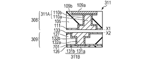
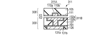
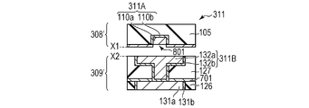
- Fig. 7A is a schematic cross-sectional view of a bonding portion of the solid-state image pickup device according to Embodiment 1.
- FIG. 7B is a schematic cross-sectional view of the bonding portion of the solid-state image pickup device according to Embodiment 1.
- Fig. 7C is a schematic cross-sectional view of a bonding portion of the solid-state image pickup device according to Embodiment 1.
- Fig. 7D is a schematic cross-sectional view of the bonding portion of the solid-state image pickup device according to Embodiment 1.
- Fig. 8A is a schematic cross-sectional view of a bonding portion of a solid-state image pickup device according to Embodiment 2.
- Fig. 8B is a schematic cross-sectional view of the bonding portion of the solid-state image pickup device according to Embodiment 2.
- Fig. 8A is a schematic cross-sectional view of a bonding portion of a solid-state image pickup device according to Embodiment 2.
- Fig. 8B is a schematic cross-sectional view of the bonding portion of the solid-state image pickup device according to Embodiment 2.
- FIG. 8C is a schematic cross-sectional view of a bonding portion of the solid-state image pickup device according to Embodiment 2.
- Fig. 8D is a schematic cross-sectional view of the bonding portion of the solid-state image pickup device according to Embodiment 2.
- Fig. 8E is a schematic cross-sectional view of a bonding portion of the solid-state image pickup device according to Embodiment 2.
- Fig. 8F is a schematic cross-sectional view of the bonding portion of the solid-state image pickup device according to Embodiment 2.
- Fig. 8G is a schematic cross-sectional view of a bonding portion of the solid-state image pickup device according to Embodiment 2.
- FIG. 8H is a schematic cross-sectional view of the bonding portion of the solid-state image pickup device according to Embodiment 2.
- Fig. 9A is a schematic cross-sectional view illustrating a step of a method for manufacturing the bonding portion according to Embodiment 2.
- Fig. 9B is a schematic cross-sectional view illustrating a step of the method for manufacturing the bonding portion according to Embodiment 2.
- Fig. 9C is a schematic cross-sectional view illustrating a step of the method for manufacturing the bonding portion according to Embodiment 2.
- Fig. 10A is a schematic cross-sectional view of a bonding portion of a solid-state image pickup device according to Embodiment 3.
- Fig. 10A is a schematic cross-sectional view of a bonding portion of a solid-state image pickup device according to Embodiment 3.
- FIG. 10B is a schematic cross-sectional view of a bonding portion of the solid-state image pickup device according to Embodiment 3.
- Fig. 10C is a schematic cross-sectional view of a bonding portion of the solid-state image pickup device according to Embodiment 3.
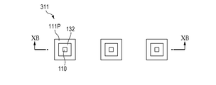
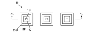
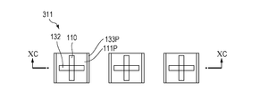
- Fig. 11A is a schematic plan view illustrating a bonding portion of the solid-state image pickup device according to Embodiment 3.
- Fig. 11B is a schematic plan view illustrating a bonding portion of the solid-state image pickup device according to Embodiment 3.
- Fig. 11C is a schematic plan view illustrating a bonding portion of the solid-state image pickup device according to Embodiment 3.
- a solid-state image pickup device of the present invention has a first substrate provided with photoelectric converters on its primary face, a first wiring structure having first bonding portions, each of which contains a conductive material, a second substrate provided with a part of a peripheral circuit on its primary face, and a second wiring structure having second bonding portions, each of which contains a conductive material.
- the first bonding portion and the second bonding portion are bonded to each other so that the first substrate, the first wiring structure, the second wiring structure, and the second substrate are disposed in this order.
- the conductive material of the first bonding portion and the conductive material of the second bonding portion are surrounded with diffusion preventing films for the respective conductive materials.
- the primary face of the first substrate and the primary face of the second substrate are substrate surfaces on which transistors are formed.
- Opposite side faces (opposite side surface) facing the respective primary faces (primary surfaces) are a back face (back surface) of the first substrate and a back face (back surface) of the second substrate.
- an upward direction indicates a direction from the back face toward the primary face of the substrate
- a downward direction and a depth direction each indicate a direction from the primary face toward the back face of the substrate.
- a wire having a single damascene structure is formed by a single damascene method in which a groove to be used for a wire is formed in an interlayer insulating film, and a conductive material, such as a barrier metal or copper, is filled in the groove, so that a wire buried in the interlayer insulating film is obtained.
- a wire having a dual damascene structure is formed such that a wire and a via are integrally formed so as to be buried in an interlayer insulating film.
- the wire having a dual damascene structure is formed by a dual damascene method in which grooves to be used for a wire and a via are formed in an interlayer insulating film, and a conductive material, such as a barrier metal or copper, is filled in the grooves.
- Embodiment 1 of the present invention will be described with reference to Figs. 1 to 6B.
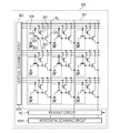
- a circuit of a solid-state image pickup device according to Embodiment 1 will be described with reference to Fig. 3.
- the solid-state image pickup device shown in Fig. 3 has a pixel portion 301 in which a plurality of photoelectric converters is arranged and a peripheral circuit portion 302 having a peripheral circuit which includes a control circuit driving readout of a signal from the pixel portion 301 and a signal processing circuit processing a readout signal.
- photoelectric converters 303, transfer transistors 304, amplification transistors 306, and reset transistors 307 are arranged.
- a structure including at least one photoelectric converter 303 is defined as a pixel.
- One pixel of this embodiment includes one photoelectric converter 303, one transfer transistor 304, one amplification transistor 306, and one reset transistor 307.
- a source of the transfer transistor 304 is connected to the photoelectric converter 303, and a drain region of the transfer transistor 304 is connected to a gate electrode of the amplification transistor 306.
- a node which is the same as the gate electrode of this amplification transistor 306 is defined as a node 305.
- the reset transistor 307 is connected to the node 305 and sets the electric potential thereof to an arbitrary electric potential (such as, a reset electric potential).
- the amplification transistor 306 is a part of a source follower circuit and outputs a signal corresponding to the electric potential of the node 305 to a signal line RL.
- the node 305 may also be called a floating diffusion in some cases.
- the peripheral circuit portion 302 indicates a region other than the pixel portion 301.
- a peripheral circuit including a readout circuit and a control circuit is disposed in the peripheral circuit portion 302.
- the peripheral circuit has a vertical scanning circuit VSR which is a control circuit supplying control signals to the gate electrodes of the transistors of the pixel portion 301.
- the peripheral circuit has a readout circuit RC which maintains signals outputted from the pixel portion 301 and performs signal processing, such as amplification, addition, and AD conversion.
- the peripheral circuit has a horizontal scanning circuit HSR which is a control circuit controlling the timing for sequentially outputting signals from the readout circuit RC.
- the solid-state image pickup device is formed by bonding two members to each other.
- the two members are a first member 308 having a first substrate 101 and a second member 309 having a second substrate 121.
- the photoelectric converters 303 and the transfer transistors 304 of the pixel portion 301 are arranged on the first substrate, and the amplification transistors 306 and the reset transistors 307 of the pixel portion 301 and at least a part of the peripheral circuit are arranged on the second substrate.
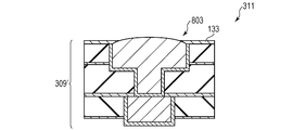
- a control signal from the peripheral circuit of the second member 309 to the gate electrode of the transfer transistor 304 of the first member 308 is supplied via a bonding portion 310.
- the structure of the bonding portion 310 will be described later.
- a signal generated in the photoelectric converter 303 of the first member 308 is read out at the drain region of the transfer transistor 304, that is, at the node 305.
- the node 305 includes the structure formed in the first member 308 and the structure formed in the second member 309.
- the area of the photoelectric converter 303 can be increased, and hence the sensitivity can be improved.
- the number of the photoelectric converters 303 can be increased, and hence the number of pixels can be increased.
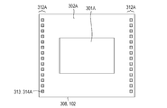
- FIG. 2A shows a plan layout of the first member 308, that is, the first substrate 101
- Fig. 2B shows a plan layout of the second member 309, that is, the second substrate 121.
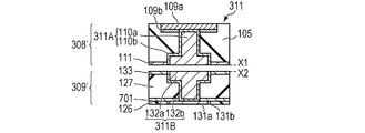
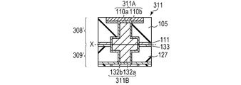
- a pixel portion 301A in which photoelectric converters are arranged and pad portions 312A in each of which pads 313 are arranged.
- the photoelectric converters 303, the transfer transistors 304, the bonding portions 310, and bonding portions 311 shown in Fig. 3 are disposed.
- bonding portions 314A for connection to the second member 309 are disposed at the same position as those of the pads 313 when viewed along a direction perpendicular to the primary face of the substrate 101.
- An external terminal is connected to the pad 313.
- the pads 313 are disposed in the solid-state image pickup device and include pads, each of which outputs a signal (image signal) based on a charge generated in the photoelectric converter, and pads to each of which a voltage or the like supplied from the outside to drive the peripheral circuit is inputted.
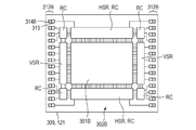
- a pixel portion 301B, the peripheral circuit portion 302, and pad portions 312B are disposed in the second member 309.
- a part of a pixel circuit is disposed in the pixel portion 301B, and the amplification transistors 306, the reset transistors 307, and the bonding portions 310 and 311 shown in Fig. 3 are disposed therein.
- a part of the peripheral circuit is disposed in the peripheral circuit portion 302, and the horizontal scanning circuits HSR, the vertical scanning circuits VSR, and the readout circuits RC are disposed therein.
- Bonding portions 314B for connection to the first member and protective diode circuits 315 are disposed in the pad portions 312B.
- first member 308 and the second member 309 which have the plan layouts shown in Fig. 2A and Fig. 2B, respectively, are bonded to each other to form the solid-state image pickup device of this embodiment.
- the pixel portion 301A and the pixel portion 301B are disposed so as to overlap with each other.
- bonding portions 314A and the bonding portions 314B are bonded to each other, and the bonding portions 310 and the bonding portions 311 of the first member are bonded to the bonding portions 310 and the bonding portions 311 of the second member, respectively.
- a region of the first member 308 corresponding to a peripheral circuit portion 302B of the second member 309 is indicated by a peripheral circuit portion 302A.
- a part of the scanning circuit that is, a part of the peripheral circuit, may be disposed in the peripheral circuit portion 302A. The structure of this bonding portion will be described later in detail.
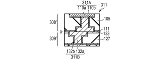
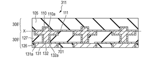
- FIG. 1 the same constituent elements as those in Figs. 2A, 2B, and 3 are designated by the same reference numerals as those described above, and description will be omitted.
- the first member 308 has a first wiring structure 149 and the first substrate 101.
- the first substrate 101 is, for example, a silicon semiconductor substrate and has a primary face 102 and a back face 103.
- the transistors are arranged on the primary face 102 of the first substrate.
- the first wiring structure 149 has interlayer insulating films 104 and 105, a gate electrode layer 107 containing gate electrodes and wires, wiring layers 109 and 110 containing wires, and a contact layer 108 containing contacts and/or vias.
- the first wiring structure 149 has a first diffusion preventing film 111.
- the numbers of the interlayer insulating film, the wiring layer, and the contact layer included in the first wiring structure 149 may be arbitrarily determined.
- the wiring layer 110 of the first wiring structure 149 contains the bonding portions 311 and 314A and is integrated with a contact layer.
- the bonding portion indicates a portion at which the conductive material of the first member and the conductive material of the second member, which collectively form an electrical connection, are boned to each other and also indicates the conductive material before bonding.
- an n-type semiconductor region 112 forming the photoelectric converter, an n-type semiconductor region 114 functioning as the drain of the transfer transistor, and an element isolation structure 119 are disposed in the first substrate 101.
- the transfer transistor is formed of the n-type semiconductor region 112, the n-type semiconductor region 114, and a gate electrode 113 contained in the gate electrode layer 107. A charge stored in the n-type semiconductor region 112 is transferred to the n-type semiconductor region 114 by the gate electrode 113.
- the photoelectric converter may be a buried photodiode further having a p-type semiconductor region or a photogate and may be appropriately changed.
- a planarizing layer 115, a color filter layer 116 containing a plurality of color filters, a planarizing layer 117, and a microlens layer 118 containing a plurality of microlenses are disposed in this order in the pixel portion 301 at a back face 103 side of the first substrate 101.
- each of the color filters and each of the microlenses are provided for one photoelectric converter, that is, are provided in each pixel, one color filter and one microlens may be provided for a plurality of pixels.
- the solid-state image pickup device of this embodiment is a so-called back-side illumination-type solid-state image pickup device in which light is incident from a microlens layer 118 side and is received by a photoelectric converter.
- the pads 313 and openings 100 which expose the pads 313 for connection to an external terminal are provided.
- the bonding portions 314A each of which transmits a voltage inputted from the pad 313 to the second member 309, are disposed.
- the bonding portions 314A are contained in the wiring layer 110 as is the bonding portions of the pixel portion.
- an optional circuit element 120 is provided in a region corresponding to the peripheral circuit portion 302B of the second member 309.
- the second member 309 has a second wiring structure 150 and the second substrate 121.
- the second substrate 121 is, for example, a silicon semiconductor substrate and has a primary face 122 and a back face 123.
- the transistors are arranged on the primary face 102 of the second substrate.
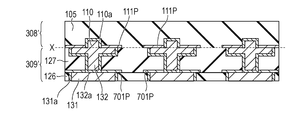
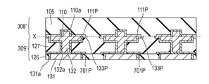
- the second wiring structure 150 has interlayer insulating films 124 to 127, a gate electrode layer 128 containing gate electrodes and wires, wiring layers 130, 131, and 132 containing wires, and a contact layer 129 containing contacts and/or vias.
- the second wiring structure 150 has a second diffusion preventing film 133.
- the numbers of the interlayer insulating film, the wiring layer, and the contact layer included in the second wiring structure 150 may be arbitrarily determined.
- the wiring layers 131 and 132 of the second wiring structure 150 are each integrated with a contact layer.
- the wiring layer 132 contains the bonding portions 311 and 314B.
- a well 135 forming the amplification transistor which forms the pixel circuit, an n-type semiconductor region 138 forming source/drain regions of the amplification transistor, and an element isolation structure 136 are disposed in the second substrate 121.
- the amplification transistor is disposed in the well 135 and is formed of a gate electrode 137 contained in the gate electrode layer 128 and the n-type semiconductor region 138 forming the source/drain regions.
- the first member 308 is connected to the gate electrodes 137 of the amplification transistors through the bonding portions 311.
- the bonding portion 311 and the gate electrode 137 of the amplification transistor are connected to each other through the wire and the via of the wiring layer 132, the wire and the via of the wiring layer 131, the wire of the wiring layer 130, and the contact of the contact layer 129.
- the node 305 shown in Fig. 3 is formed of the n-type semiconductor region 114, the wires and the vias of the wiring layers 109, 110, 132, 131, and 130, the contacts of the contact layers 108 and 129, and the gate electrode 137 shown in Fig. 1.
- Other circuits (such as the reset transistor) of the pixel portion 301 are not shown in the figure.
- Fig. 1 shows an n-type transistor and a p-type transistor in an optional circuit included in the peripheral circuit.
- An n-type transistor formed of a gate electrode 140 contained in the gate electrode layer 128 and n-type source/drain regions 141 is disposed in a p-type well 139.
- a p-type transistor having a gate electrode 143 contained in the gate electrode layer 128 and a p-type semiconductor region 144 forming p-type source/drain regions is disposed in an n-type well 142.
- the protective diode circuit 315 inputting a signal from the pad 313 of the first member 308 and the bonding portion 314B for connection to the first member 308.
- the bonding portion 314B is contained in the wiring layer 132 as is the bonding portion of the pixel portion.
- Two diodes 145 and 146 each formed from the semiconductor region and two resistors 147 and 148 formed from the gate electrode layer 128 are contained in the protective diode circuit 315 of this embodiment. A commonly-used protective diode circuit can be applied to this protective diode circuit 315.
- the primary face 102 of the first substrate 101 and the primary face 122 of the second substrate 121 are disposed to face each other with the first and second wiring structures provided therebetween (facing arrangement). That is, the first substrate, the first wiring structure, the second wiring structure, and the second substrate are disposed in this order.
- an upper face of the first wiring structure 149 and an upper face of the second wiring structure 150 are bonded to each other at a bonding plane X. That is, the first member 308 and the second member 309 are bonded to each other at the bonding plane X.
- the bonding plane X is formed from the upper face of the first wiring structure 149 and the upper face of the second wiring structure 150.
- the bonding portions disposed in the respective members are bonded to each other at the bonding plane X and ensure the conduction between the members.
- the pad 313 of the solid-state image pickup device for exchanging a signal with the outside is disposed above the primary face 122 of the second member 309, and the opening 100 is provided at a first member 308 side.
- the wiring layer 109 is formed of wires (aluminum wires) primarily composed of aluminum
- the wiring layer 110 is formed of wires (copper wires) primarily composed of copper and has a dual damascene structure.
- the wiring layer 130 is formed of copper wires and has a single damascene structure.
- the wiring layers 131 and 132 are formed of copper wires and each have a dual damascene structure.
- the bonding portion 311 and the bonding portion 314A formed of the wires contained in the wiring layer 110 are bonded to the bonding portion 311 and the bonding portion 314B formed of the wires contained in the wiring layer 132, respectively, at the bonding plane X by metal bonding.
- the pad 313 for connection to an external terminal is disposed in the same layer as that of the wiring layer 109, that is, at the same height as that thereof, and is a conductive material primarily composed of aluminum.
- the height of this wiring layer 109 and that of the pad 313 are each a height from the primary face 102 of the first substrate 101.
- Figs. 4A and 4B are each a schematic cross-sectional view showing a step of manufacturing the first member 308, Figs. 5A and 5B are each a schematic cross-sectional view showing a step of manufacturing the second member 309, and Figs. 6A and 6B are each a schematic cross-sectional view showing a manufacturing step performed after the first member 308 and the second member 309 are bonded to each other.
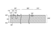
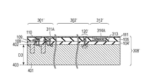
- a structure to be later formed into the first member 308 shown in Fig. 1 is represented by 308', and portions to be formed into the pixel portion 301, the peripheral circuit portion 302, the pad portion 312, and the circuit element 120, which is a part of the peripheral circuit, shown in Fig. 1 are represented by 301', 302', 312', and 120', respectively.
- a semiconductor substrate is provided, and elements are formed in the semiconductor substrate.
- a semiconductor substrate 401 of a thickness D3 having a primary face 402 and a back face 403 is provided.
- the semiconductor substrate 401 is, for example, a silicon semiconductor substrate.
- the element isolation structure 119 is formed in the semiconductor substrate 401.
- the element isolation structure 119 contains an insulating material, such as a silicon oxide film, and has, for example, a LOCOS or an STI structure.
- a well (not shown) having an arbitrary conductivity type is formed in the semiconductor substrate 401.
- the n-type semiconductor regions 112 and 114 and a p-type semiconductor region (not shown), which form a photoelectric converter and a transistor, are formed.
- the gate electrode layer 107 containing the gate electrode 113 of the transfer transistor is formed.
- the gate electrode layer is formed, for example, by deposition and patterning of a polysilicon layer and may contain a wire as well as the gate electrode. Methods for forming the gate electrode, element isolation, and semiconductor region may be performed in accordance with a general semiconductor process, and detailed description will be omitted.
- the structure shown in Fig. 4A is obtained by the steps described above.
- the wiring structure is formed on the primary face 402 of the semiconductor substrate 401.
- a film to be formed into an interlayer insulating film 104' is formed so as to cover the gate electrode layer 107.
- films of a barrier metal and tungsten are formed, and excessive parts of the films thereof are removed, thereby forming the interlayer insulating film 104' and the contact layer 108.
- films of a barrier metal and aluminum are formed on the interlayer insulating film 104', followed by patterning, so that the wiring layer 109 is formed.
- a film to be formed into the interlayer insulating film 105 is formed so as to cover the wiring layer 109, and a film to be formed into the first diffusion preventing film 111 is formed.
- the wiring layer 110 is formed by a dual damascene method. Grooves for wires and grooves (holes) for vias are formed in a laminate of the film to be formed into the interlayer insulating film 105 and the film to be formed into the first diffusion preventing film 111. A film of a barrier metal having a diffusion preventing function and a film of copper are formed so as to fill the grooves.
- the wiring layer 110 is formed by removing excessive barrier metal and copper, and the interlayer insulating film 105 and the first diffusion preventing film 111 are formed.
- the first diffusion preventing film 111 has openings to expose wires.
- the first diffusion preventing film 111 can be simultaneously planarized by etching or chemical mechanical polishing (CMP) performed when a barrier metal and copper are removed.
- CMP chemical mechanical polishing
- the upper face of the first planarized diffusion preventing film 111 thus planarized has a sufficient flatness for subsequent bonding.
- the upper face of the wiring structure is formed of the upper face of the first diffusion preventing film 111 and the upper face of wiring layer 110.
- the interlayer insulating film 104' is later formed into the interlayer insulating film 104 shown in Fig. 1.
- the interlayer insulating films 104' and 105 are each a silicon oxide film.
- the interlayer insulating films 104' and 105 may also be formed, for example, of a silicon nitride film or an organic resin.
- the contact 108 is formed, for example, from tungsten.
- the wiring layer 110 contains the bonding portion 314A and a bonding portion 311A, and the wiring layer 109 contains the pad 313.
- the barrier metal has a function to prevent diffusion of copper which is a conductive material and is formed, for example, of tantalum or tantalum nitride.
- the first diffusion preventing film 111 is formed of a film which has a diffusion preventing function to the conductive material of the wiring layer 110 containing the bonding portion and is a high-density inorganic insulating film.
- the diffusion preventing film is a silicon nitride film or a silicon carbide film.
- Methods for manufacturing these wiring layer, contact layer, and interlayer insulating film can be performed in accordance with a general semiconductor process, and detailed description will be omitted.
- the structure shown Fig. 4B is obtained by the steps described above. In Fig. 4B, the portions represented by reference numerals 104', 105, 106, 108, 109, and 110 are later used to form the first wiring structure 149 shown in Fig. 1.
- the bonding portion 311A later forms the bonding portion 311.
- the upper face of the first wiring structure 149 which later forms the bonding plane X shown in Fig. 1 is formed of the upper face of the first diffusion preventing film 111 and the upper face of each wire of the wiring layer 110. The structure of this upper face will be described later in detail.
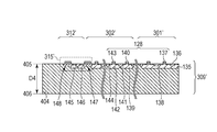
- a structure to be later formed into the second member 309 shown in Fig. 1 is represented by reference numeral 309', and portions to be formed into the pixel portion 301, the peripheral circuit portion 302, the pad portion 312, and the protective diode circuit 315 shown in Fig. 1 are represented by reference numerals 301', 302', 312', and 315', respectively.
- a wiring structure is formed on a primary face 405 of a semiconductor substrate 404.
- a film to be formed into the interlayer insulating film 124 is formed so as to cover the gate electrode 128.
- a film of a barrier metal and a film of tungsten are formed, and the interlayer insulating film 124 and the contact layer 129 are formed by removing excessive parts of the films of a barrier metal and tungsten.
- a film to be formed into the interlayer insulating film 125 is formed on the interlayer insulating film 124.
- the wiring layer 130 is formed by a single damascene method.
- Grooves for wire are formed in the film to be formed into the interlayer insulating film 125, and a film of a barrier metal having a diffusion preventing function and a film of copper are formed so as to fill the grooves.
- the wiring layer 130 is formed by removing excessive barrier metal and copper, and the interlayer insulating film 125 is formed.
- a film to be formed into the interlayer insulating film 126 is formed so as to cover the interlayer insulating film 125 and the wiring layer 130.
- the wiring layer 131 is formed by a dual damascene method.
- grooves for wires and vias are formed in the film to be formed into the interlayer insulating film 126.
- a film of a barrier metal having a diffusion preventing function and a film of copper are formed so as to fill the grooves.
- the wiring layer 131 is formed by removing excessive barrier metal and copper, and the interlayer insulating film 126 is formed.
- a film to be formed into the interlayer insulating film 127 and a film to be formed into the second diffusion preventing film 133 are formed so as to cover the interlayer insulating film 126 and the wiring layer 131.
- the wiring layer 132 is formed by a dual damascene method.
- grooves for wires and vias are formed in the films to be formed into the interlayer insulating film 127 and the second diffusion preventing film 133, and a film of a barrier metal having a diffusion preventing function and a film of copper are formed so as to fill the grooves.
- the wiring layer 132 is formed by removing excessive parts of the film of copper and the film of a barrier metal having a diffusion preventing function.
- the barrier metal has a diffusion preventing function to copper which is a conductive material and is formed, for example, of tantalum or tantalum nitride.
- the interlayer insulating film 127 and the second diffusion preventing film 133 are formed.
- the second diffusion preventing film 133 has openings so as to expose wires.
- the second diffusion preventing film 133 can be simultaneously planarized by etching or CMP performed when a barrier metal and copper are removed.
- the upper face of the wiring structure is formed of the upper face of the second diffusion preventing film 133 and the upper face of the wiring layer 132.
- the interlayer insulating films 124 to 127 each may also be formed, for example, of a silicon nitride film or an organic resin.
- the contact 129 is formed, for example, of tungsten.
- the wiring layer 130 is formed of wires primarily composed of copper and has a single damascene structure.
- the wiring layers 131 and 132 are each formed of wires primarily composed of copper and each have a dual damascene structure.
- the wiring layer 132 contains the bonding portion 314B and a bonding portion 311B.
- FIG. 5B is obtained by the steps described above.
- the portions represented, for example, by reference numerals 124 to 127 and 129 to 133 are later used to form the second wiring structure 150 shown in Fig. 1.
- the bonding portion 311B later forms the bonding portion 311.
- the upper face of the second wiring structure 150 which later forms the bonding plane X shown in Fig. 1 is formed of the upper face of the interlayer insulating film 127 and the upper face of each wire of the wiring layer 132.
- the wiring layer 132 is also a conductive material used as the bonding portion. That is, the upper face of the second wiring structure 150 contains the upper face of the conductive material. The structure of this upper face will be described later in detail.
- the first member 308' and the second member 309' as shown in Figs. 4B and 5B, respectively, are bonded together so that the primary face 402 and the primary face 405 of the respective semiconductor substrates face each other. That is, the uppermost face of the wiring structure of the first member 308' and the uppermost face of the wiring structure of the second member 309' are boned to each other.
- the bonding portions 311A and 311B and the bonding portions 314A and 314B are formed of wires primarily composed of copper, when bonding is performed therebetween, metal bonding of copper may be performed.
- bonding is preferably performed in a vacuum or an inert gas atmosphere.
- plasma irradiation is preferably performed on the upper face of each wiring structure.
- bonding between the interlayer insulating films such as a silicon oxide film and/or a silicon nitride film, can be more strengthened.
- an activation method by a chemical treatment may also be used. By this bonding, the two wiring structures are united into one wiring structure which includes the copper bonding portions surrounded with the diffusion preventing films.
- the thickness of the semiconductor substrate 401 of the first member 308' is reduced at a back face 403 side.
- the reduction of the thickness may be performed by CMP or etching. Accordingly, the semiconductor substrate 401 is formed into a semiconductor substrate 407, and the thickness is changed from D3 to D1 (D1 ⁇ D3) (Fig. 6A).
- the thickness D1 of the semiconductor substrate 407 is smaller than a thickness D4 of the semiconductor substrate 404.
- a planarizing layer 409 formed of a resin, a color filter layer 410, a planarizing layer 411 formed of a resin, and a microlens layer 412 are formed in this order on a back face 408 of the semiconductor substrate 407.
- Methods for manufacturing these planarizing layer, color filter layer, and microlens layer can be performed in accordance with a general semiconductor process, and detailed description will be omitted.
- the microlens layer may be formed to the region 312' which is to be formed into the pad portion.
- the structure shown in Fig. 6B is obtained by the steps described above.
- the opening 100 is formed to expose the pad 313.
- a photoresist mask having an arbitrary opening is formed on the microlens layer 412 using a photolithographic technique.
- the microlens layer 412, the planarizing layer 411, the color filter layer 410, the planarizing layer 409, the semiconductor substrate 407, and the interlayer insulating film 104' are partially removed, thereby forming the opening 100 to expose the pad 313.
- the microlens layer 118, the planarizing layers 117 and 115, the color filter layer 116, the first substrate 101, and the interlayer insulating film 104 are formed.
- the structure shown in Fig. 1 is obtained.
- the semiconductor substrate 404, the primary face 405, a back face 406, and the thickness D4 shown in Fig. 6B correspond to the second substrate 121, the primary face 122, the back face 123, and the thickness D2 shown in Fig. 1, respectively.
- the thickness D4 is not changed from the thickness D2 in this case, the thickness of the semiconductor substrate 404 may be reduced so that the thickness D2 is smaller than the thickness D4.
- the number of steps is increased by the reduction in thickness, the solid-state image pickup device can be miniaturized.
- Figs. 7A to 7D are each an enlarged schematic cross-sectional view of the bonding portion 311 shown in Fig. 1.
- Figs. 7A to 7D the same constituent elements as those shown in Figs. 1 to 6B are designated by the same reference numerals as those described above, and description will be omitted.
- Fig. 7A shows the state before the first member and the second member are bonded to each other
- Fig. 7B shows the state in which the two members are bonded to each other (Fig. 6A).
- the first member 308' has the wiring layer 109, the wiring layer 110, and the first diffusion preventing film 111.
- the wring layer 109 contains aluminum 109a and a barrier metal 109b
- the wiring layer 110 contains copper 110a and a barrier metal 110b.
- the second member 309' has the wiring layer 131, the wiring layer 132, and the second diffusion preventing film 133.
- the wiring layer 131 contains copper 131a and a barrier metal 131b
- the wiring layer 132 contains copper 132a and a barrier metal 132b.
- the bonding portion contains copper having a higher diffusion coefficient than that of aluminum as a conductive material.
- the conductive material is not limited to copper and may be selected from alloys primarily composed of copper, other metals, such as Au, and alloys thereof.
- a barrier metal for copper functions as a diffusion preventing film having a capability of preventing diffusion of copper.
- metals, such as a tantalum, manganese, niobium, and chromium, and alloys thereof may be mentioned, and a tantalum nitride film also has a barrier function.
- the first diffusion preventing film and the second diffusion preventing film for example, a silicon nitride film, a silicon carbide film, silicon carbonitride film, or a silicon oxynitride film may be mentioned.
- the copper 110a is surrounded with the barrier metal 110b except for the portion exposed to a plane X1.
- the copper 132a is surrounded with the barrier metal 132b except for the portion exposed to a plane X2.
- the plane X1 is the upper face of the first wiring structure 149
- the plane X2 is the upper face of the second wiring structure 150.
- the plane X1 and the plane X2 form the bonding plane X
- the first member 308' and the second member 309' are bonded to each other.
- the copper 110a and the copper 132a are metal-bonded together.
- the copper 110a and the copper 132a are surrounded with the barrier metal 110b and the barrier metal 132b, respectively, each of which is the diffusion preventing film having a diffusion preventing function to copper.
- a solid-state image pickup device capable of suppressing the generation of dark current and/or leakage current can be provided.
- Fig. 7C is a schematic cross-sectional view showing the case in which in the structure shown in Fig. 7A, the positions of the wiring layer 110 and the wiring layer 132, which form the bonding portion, are shifted.
- the conductive material can also be surrounded with the diffusion preventing films at the bonding portion.
- the copper 110a and the copper 132a are collectively surrounded with the barrier metal 110b and the barrier metal 132b, each of which is the diffusion preventing film, and the first diffusion preventing film 111 and the second diffusion preventing film 133.
- the present invention is not limited to the steps described in the manufacturing method according to this embodiment, and the order of the steps may also be changed.
- the order of manufacturing the first member 308 and the second member 309 may be appropriately determined.
- An SOI substrate may also be applied to each of the semiconductor substrates 401 and 404.
- the first member 308 and the second member 309 are separately purchased as the substrates for the solid-state image pickup device and are then bonded together.
- FIGS. 8A to 8H are each a schematic cross-sectional view focusing on a bonding portion corresponding to that shown in Figs. 7A to 7D.
- constituent elements similar to those shown in Figs. 1 to 7D are designated by the same reference numerals as those described above, and description will be omitted.
- Fig. 8A is a schematic cross-sectional view corresponding to that shown in Fig. 7A
- Fig. 8B is a schematic cross-sectional view corresponding to that shown in Fig. 7B.
- the differences from Fig. 7A are that the wiring layer 110 has a smaller exposed area than that of the wiring layer 132 and that the second member 309' has no second diffusion preventing film 133.
- the structure shown in Fig. 8A is only a partial cross-section thereof, the area of the wiring layer 110 at the plane X1 is smaller than the area of the wiring layer 132 at the plane X2.
- the copper 110a and the copper 132a are also surrounded with the barrier metals 110b and 132b, each of which is the diffusion preventing film, and the first diffusion preventing film 111.
- Fig. 8C is a schematic cross-sectional view corresponding to that shown in Fig. 8A
- Fig. 8D is a schematic cross-sectional view corresponding to that shown in Fig. 8B.
- the difference from Fig. 8A is that the wiring layer 110 has a concave portion 801 at the plane X1.
- the first diffusion preventing film 111 is disposed on the interlayer insulating film 105 and the wiring layer 110 and has an opening corresponding to the wiring layer 110.
- the copper 110a and the copper 132a are also surrounded with the barrier metals 110b and 132b, each of which is the diffusion preventing film, and the first diffusion preventing film 111.
- the concave portion 801 has a step corresponding to the thickness of the first diffusion preventing film 111, the step may be increased, for example, by partially removing the copper 110a.
- the bonding plane X of the bonding may have a flat face as shown in Fig. 8D.
- Fig. 8E is a schematic cross-sectional view corresponding to that shown in Fig. 8C
- Fig. 8F is a schematic cross-sectional view corresponding to that shown in Fig. 8D.
- the difference from Fig. 8C is that the wiring layer 110 has a convex portion 802 at the plane X1.
- the copper 110a has a convex portion protruding by a thickness D from the plane X1 formed of the first diffusion preventing film 111 and the like.
- the copper 110a and the copper 132a are also surrounded with the barrier metals 110b and 132b, each of which is the diffusion preventing film, and the first diffusion preventing film 111.
- the convex portion 802 may have a rectangular shape.
- the bonding plane X after the bonding may have a flat face as shown in Fig. 8F.
- Fig. 8G is a schematic cross-sectional view corresponding to that shown in Fig. 8E
- Fig. 8H is a schematic cross-sectional view corresponding to that shown in Fig. 8F.
- the differences from Fig. 8E is the following three points. That is, the three points are that the wiring layer 132 also has a convex portion 803 at the plane X2, the area of the wiring layer 110 at the plane X1 and the area of the wiring layer 132 at the plane X2 are equal to each other, and the second member 309' has the second diffusion preventing film 133.
- the copper 110a has a convex portion protruding from the plane X1 by a thickness D1
- the copper 132a has a convex portion protruding from the plane X2 by a thickness D2.
- the copper 110a and the copper 132a are also surrounded with the barrier metals 110b and 132b, each of which is the diffusion preventing film, the first diffusion preventing film 111, and the second diffusion preventing film 133.
- a gap 804 is formed between the first member 308' and the second member 309'.
- the copper 110a and the copper 132a are in contact with the gap 804, copper may diffuse at the interface with this gap 804 in some cases.
- the first diffusion preventing film 111 and the second diffusion preventing film 133 are provided, diffusion of copper to the substrate sides of the first member 308' and the second member 309' can be suppressed.
- the gap 804 may not be formed in some cases after the first member 308' and the second member 309' shown in Fig. 8G are bonded together.
- the interlayer insulating film 126, the wiring layer 131, and the interlayer insulating film 127 are formed.
- the wiring layer 132 is formed in the interlayer insulating film 127 by a dual damascene method.
- the copper 132a having a convex portion(a protrusion portion) can be formed by adjusting a polishing speed and a slurry in the case of using a CMP method or by adjusting an etching gas and the like in the case of using etching (Fig. 9A).
- a film 133' which covers the convex portion and which is to be formed into the second diffusion preventing film is formed (Fig. 9B) and is then partially removed by etching method or CMP method, so that the second diffusion preventing film 133 and the convex portion 803 can be formed (Fig. 9C).
- the interlayer insulating film 126 and the interlayer insulating film 127 are each formed of a plurality of insulating films, and a diffusion preventing film 701 covering the upper face of the wiring layer 131 is formed. As described above, the structure of the interlayer insulating film may be appropriately determined.
- FIGS. 10A to 10C are schematic cross-sectional views of the bonding portions described with reference to Figs. 8A to 8H.
- constituent elements similar to those shown in Figs. 1 to 7D are designated by the same reference numerals as those described above, and description will be omitted.
- Figs. 10A and 10B correspond to each other and are each a schematic cross-sectional view in which a plurality of bonding portions shown in Fig. 8B or 8D is arranged.
- Fig. 10C shows the modification of the structure shown in Fig. 10B.
- the first diffusion preventing film 111 is formed common to a plurality of the bonding portions 311.
- a first diffusion preventing film 111P is formed by patterning so as to surround the periphery of the corresponding bonding portion, and the first diffusion preventing film 111 between the bonding portions 311 is removed.
- a second diffusion preventing film 133P is further provided, and the second diffusion preventing film 133P is formed by patterning so as to surround the periphery of the corresponding bonding portion as in the case of the first diffusion preventing film 111P.
- the first diffusion preventing film is formed of a silicon nitride film, and the interlayer insulating film is formed of silicon oxide, the first diffusion preventing film has a dielectric constant higher than that of the interlayer insulating film.
- the parasitic capacitance thereof is increased.
- the parasitic capacitance between wires can be reduced by the structure shown in Fig. 10B.
- the second diffusion preventing film 133P is provided as shown in Fig. 10C
- the parasitic capacitance can be reduced.
- the diffusion preventing film 701 may also be patterned as shown in Figs. 10B and 10C.
- Figs. 11A to 11C are each a schematic plan view of an outer edge of each structure to illustrate the positional relationship of the wiring layer 110, the wiring layer 132, the first diffusion preventing film, and the second diffusion preventing film at the bonding portion 311. In other words, these views show the arrangement of each structure at the bonding plane X.
- constituent elements similar to those shown in Figs. 1 to 10C are designated by the same reference numerals as those described above, and description will be omitted.
- Fig. 11A is a schematic plan view corresponding to Fig. 10B.
- the line XB-XB shown in Fig. 11A corresponds to the cross-section taken along the bonding plane X of Fig. 10B.
- the first diffusion preventing film 111P has the largest area and covers the wiring layer 132. That is, a face at which copper of the wiring layer 132 is exposed corresponds to the first diffusion preventing film 111P and the wiring layer 110.
- copper can be easily covered with the diffusion preventing film.
- Fig. 11B and Fig. 11C are schematic plan views corresponding to Fig. 10C.
- the line XC-XC shown in Fig. 11B and Fig. 11C corresponds to the cross-section taken along the bonding plane X shown in Fig. 10C.
- the size of the pattern is increased from the wiring layer 110, the wiring layer 132, the first diffusion preventing film 111P, and the second diffusion preventing film 133P in this order.
- a face at which copper of the wiring layer 132 is exposed corresponds to the first diffusion preventing film 111P and the wiring layer 110, and copper can be easily covered with the diffusion preventing film.
- Fig. 11C has different patterns of the wiring layer 110 and the wiring layer 132 from those shown in Fig. 11B.
- the patterns of the wiring layer 110 and the wiring layer 132 have long sides in a first direction and a second direction different therefrom, respectively.
- the first diffusion preventing film, the second diffusion preventing film, and the bonding portion each may have an arbitrary shape, and the shapes thereof may be appropriately selected.
- an image pickup system incorporating a solid-state image pickup device will be described by way of example.
- a camera includes the solid-state image pickup device of the present invention and a processing portion which processes a signal outputted from the solid-state image pickup device.
- This processing portion may include, for example, an A-D converter and a processor processing a digital data outputted therefrom.
- a solid-state image pickup device capable of suppressing the generation of dark current and/or leakage current can be provided.
- the present invention is not limited to the structures described in the specification and may also be applied to the case in which the pixel circuit is changed and only the photoelectric converters are arranged for the first member. Furthermore, the present invention may be appropriately applied, for example, to the structure in which the conductive and/or circuit type is changed to a reversed type, the structure in which a wiring layer and an interlayer insulating film are further provided, and the case in which a single damascene structure is changed to a dual damascene structure. In addition, the structures of the embodiments may also be used in combination.
- the present invention is not limited to a solid-state image pickup device and may also be applied to common semiconductor devices, such as a DRAM.
Landscapes
- Engineering & Computer Science (AREA)
- Power Engineering (AREA)
- Physics & Mathematics (AREA)
- Computer Hardware Design (AREA)
- Microelectronics & Electronic Packaging (AREA)
- Electromagnetism (AREA)
- Condensed Matter Physics & Semiconductors (AREA)
- General Physics & Mathematics (AREA)
- Solid State Image Pick-Up Elements (AREA)
- Transforming Light Signals Into Electric Signals (AREA)
- Internal Circuitry In Semiconductor Integrated Circuit Devices (AREA)
Abstract
Description
302 peripheral circuit portion
308 first member
309 second member
149 first wiring structure
150 second wiring structure
311 bonding portion
314 bonding portion
101 first substrate
121 second substrate
X bonding plane
111 first diffusion preventing film
133 second diffusion preventing film
Claims (14)
- A solid-state image pickup device comprising:
a first substrate provided with a photoelectric converter disposed on its primary face;
a first wiring structure which is disposed on the primary face of the first substrate and which has a first bonding portion containing a conductive material;
a second substrate provided with, on its primary face, a part of a peripheral circuit including a control circuit and a readout circuit reading out a signal based on a charge of the photoelectric converter; and
a second wiring structure which is disposed on the primary face of the second substrate and which has a second bonding portion containing a conductive material,
wherein the first bonding portion and the second bonding portion are bonded so that the first substrate, the first wiring structure, the second wiring structure, and the second substrate are disposed in this order, and
the conductive material of the first bonding portion and the conductive material of the second bonding portion are surrounded with diffusion preventing films. - The solid-state image pickup device according to Claim 1, wherein the first bonding portion contains the conductive material and a barrier metal,
the second bonding portion contains the conductive material and a barrier metal, and
the diffusion preventing films comprise the respective barrier metals. - The solid-state image pickup device according to Claim 2, wherein the first wiring structure has an interlayer insulating film in which the first bonding portion is disposed, and
the barrier metal of the first bonding portion is disposed between the conductive material of the first bonding portion and the interlayer insulating film. - The solid-state image pickup device according Claim 2 or 3, wherein the second wiring structure has an interlayer insulating film in which the second bonding portion is disposed, and
the barrier metal of the second bonding portion is disposed between the conductive material of the second bonding portion and the interlayer insulating film. - The solid-state image pickup device according to one of Claims 1 to 4,
wherein the conductive materials each comprise a metal having a higher diffusion coefficient than that of aluminum or an alloy containing the metal. - The solid-state image pickup device according to Claim 5, wherein the conductive materials each comprise copper or an alloy primarily composed of copper.
- The solid-state image pickup device according to one of Claims 1 to 6,
wherein the diffusion preventing films include a first diffusion preventing film, and
the upper face of the first wiring structure is comprised of the first bonding portion and the first diffusion preventing film. - The solid-state image pickup device according to Claim 7, wherein the first diffusion preventing film is patterned to surround the periphery of the first bonding portion.
- The solid-state image pickup device according to Claim 7 or 8, wherein the first diffusion preventing film is a silicon nitride film or a silicon carbide film.
- The solid-state image pickup device according to one of Claims 1 to 6,
wherein the diffusion preventing films include a second diffusion preventing film, and
the upper face of the second wiring structure is comprised of the second bonding portion and the second diffusion preventing film. - The solid-state image pickup device according to Claim 10, wherein the second diffusion preventing film is patterned to surround the periphery of the second bonding portion.
- The solid-state image pickup device according to Claim 10 or 11, wherein the second diffusion preventing film is a silicon nitride film or a silicon carbide film.
- The solid-state image pickup device according to one of Claims 1 to 12, wherein the second substrate is further provided with an amplification transistor outputting a signal based on a charge of the photoelectric converter and a reset transistor resetting the charge of the photoelectric converter.
- An imaging system comprising: the solid-state image pickup device according to one of Claims 1 to 13; and a signal processing circuit processing a signal from the solid-state image pickup device.
Priority Applications (13)
| Application Number | Priority Date | Filing Date | Title |
|---|---|---|---|
| EP11803305.9A EP2591505A4 (en) | 2010-07-09 | 2011-07-04 | Solid-state image pickup device |
| CN201180033415.3A CN102971851B (en) | 2010-07-09 | 2011-07-04 | Solid-state image pickup apparatus |
| EP20166179.0A EP3706172A1 (en) | 2010-07-09 | 2011-07-04 | Solid-state image pickup device |
| US13/808,877 US9166090B2 (en) | 2010-07-09 | 2011-07-04 | Solid-state image pickup device |
| RU2013105505/28A RU2521224C1 (en) | 2010-07-09 | 2011-07-04 | Image acquisition solid-state device |
| US14/856,354 US9419030B2 (en) | 2010-07-09 | 2015-09-16 | Solid-state image pickup device |
| US15/209,605 US9640581B2 (en) | 2010-07-09 | 2016-07-13 | Solid-state image pickup device |
| US15/456,386 US9929202B2 (en) | 2010-07-09 | 2017-03-10 | Solid-state image pickup device |
| US15/894,258 US10217786B2 (en) | 2010-07-09 | 2018-02-12 | Solid-state image pickup device |
| US16/242,835 US10573680B2 (en) | 2010-07-09 | 2019-01-08 | Solid-state image pickup device |
| US16/777,586 US11177310B2 (en) | 2010-07-09 | 2020-01-30 | Solid-state image pickup device |
| US17/505,039 US20220037390A1 (en) | 2010-07-09 | 2021-10-19 | Solid-state image pickup device |
| US18/322,239 US20230299112A1 (en) | 2010-07-09 | 2023-05-23 | Solid-state image pickup device |
Applications Claiming Priority (2)
| Application Number | Priority Date | Filing Date | Title |
|---|---|---|---|
| JP2010-156926 | 2010-07-09 | ||
| JP2010156926A JP5451547B2 (en) | 2010-07-09 | 2010-07-09 | Solid-state imaging device |
Related Child Applications (2)
| Application Number | Title | Priority Date | Filing Date |
|---|---|---|---|
| US13/808,877 A-371-Of-International US9166090B2 (en) | 2010-07-09 | 2011-07-04 | Solid-state image pickup device |
| US14/856,354 Division US9419030B2 (en) | 2010-07-09 | 2015-09-16 | Solid-state image pickup device |
Publications (1)
| Publication Number | Publication Date |
|---|---|
| WO2012004965A1 true WO2012004965A1 (en) | 2012-01-12 |
Family
ID=45440958
Family Applications (1)
| Application Number | Title | Priority Date | Filing Date |
|---|---|---|---|
| PCT/JP2011/003796 WO2012004965A1 (en) | 2010-07-09 | 2011-07-04 | Solid-state image pickup device |
Country Status (6)
| Country | Link |
|---|---|
| US (9) | US9166090B2 (en) |
| EP (2) | EP2591505A4 (en) |
| JP (1) | JP5451547B2 (en) |
| CN (2) | CN105720067B9 (en) |
| RU (1) | RU2521224C1 (en) |
| WO (1) | WO2012004965A1 (en) |
Cited By (7)
| Publication number | Priority date | Publication date | Assignee | Title |
|---|---|---|---|---|
| CN104662662A (en) * | 2012-09-28 | 2015-05-27 | 索尼公司 | Semiconductor device and electronic instrument |
| US9153565B2 (en) | 2012-06-01 | 2015-10-06 | Taiwan Semiconductor Manufacturing Company, Ltd. | Image sensors with a high fill-factor |
| US10090349B2 (en) | 2012-08-09 | 2018-10-02 | Taiwan Semiconductor Manufacturing Company, Ltd. | CMOS image sensor chips with stacked scheme and methods for forming the same |
| FR3069371A1 (en) * | 2017-07-19 | 2019-01-25 | Stmicroelectronics (Crolles 2) Sas | ELECTRONIC DEVICE IMAGE SENSOR |
| KR20210107592A (en) * | 2011-07-05 | 2021-09-01 | 소니그룹주식회사 | Semiconductor device, fabrication method for a semiconductor device and electronic apparatus |
| US11257782B2 (en) | 2017-05-16 | 2022-02-22 | Sony Semiconductor Solutions Corporation | Method of manufacturing semiconductor device and semiconductor device |
| US11569123B2 (en) | 2011-07-05 | 2023-01-31 | Sony Corporation | Semiconductor device, fabrication method for a semiconductor device and electronic apparatus |
Families Citing this family (38)
| Publication number | Priority date | Publication date | Assignee | Title |
|---|---|---|---|---|
| CN102668081B (en) | 2009-12-26 | 2016-02-03 | 佳能株式会社 | Solid-state image pickup apparatus and image picking system |
| JP5451547B2 (en) * | 2010-07-09 | 2014-03-26 | キヤノン株式会社 | Solid-state imaging device |
| JP5994274B2 (en) * | 2012-02-14 | 2016-09-21 | ソニー株式会社 | SEMICONDUCTOR DEVICE, SEMICONDUCTOR DEVICE MANUFACTURING METHOD, AND ELECTRONIC DEVICE |
| KR101240537B1 (en) * | 2012-05-07 | 2013-03-11 | (주)실리콘화일 | Manufacture method for image sensor having 3 dimension structure |
| JP6012262B2 (en) | 2012-05-31 | 2016-10-25 | キヤノン株式会社 | Manufacturing method of semiconductor device |
| US8796805B2 (en) * | 2012-09-05 | 2014-08-05 | Taiwan Semiconductor Manufacturing Company, Ltd. | Multiple metal film stack in BSI chips |
| US8866250B2 (en) * | 2012-09-05 | 2014-10-21 | Taiwan Semiconductor Manufacturing Company, Ltd. | Multiple metal film stack in BSI chips |
| JP6128787B2 (en) * | 2012-09-28 | 2017-05-17 | キヤノン株式会社 | Semiconductor device |
| JP6017297B2 (en) * | 2012-12-14 | 2016-10-26 | オリンパス株式会社 | Manufacturing method of semiconductor device |
| KR102136845B1 (en) | 2013-09-16 | 2020-07-23 | 삼성전자 주식회사 | Stack type image sensor and fabrication method thereof |
| JP6212720B2 (en) * | 2013-09-20 | 2017-10-18 | パナソニックIpマネジメント株式会社 | Semiconductor device and manufacturing method thereof |
| TWI676279B (en) * | 2013-10-04 | 2019-11-01 | 新力股份有限公司 | Semiconductor device and solid-state imaging device |
| CN104810366B (en) * | 2014-01-26 | 2018-09-11 | 中芯国际集成电路制造(上海)有限公司 | A kind of integrated circuit and its manufacturing method |
| CN104241201B (en) * | 2014-08-28 | 2017-05-31 | 武汉新芯集成电路制造有限公司 | A kind of method of integrated power device and control device |
| CN104241200B (en) * | 2014-08-28 | 2017-03-08 | 武汉新芯集成电路制造有限公司 | A kind of power device and the integrated approach of control device |
| US10285088B2 (en) * | 2014-09-26 | 2019-05-07 | Nokia Technologies Oy | Methods and apparatus for minimization of drive testing |
| CN104599988B (en) * | 2015-01-05 | 2017-08-04 | 武汉新芯集成电路制造有限公司 | The method of integrated power device and control device |
| US10431614B2 (en) * | 2017-02-01 | 2019-10-01 | Semiconductor Components Industries, Llc | Edge seals for semiconductor packages |
| US20200144322A1 (en) * | 2017-07-18 | 2020-05-07 | Sony Semiconductor Solutions Corporation | Imaging apparatus and method of manufacturing imaging apparatus |
| US10727217B2 (en) | 2017-09-29 | 2020-07-28 | Taiwan Semiconductor Manufacturing Company, Ltd. | Method of manufacturing semiconductor device that uses bonding layer to join semiconductor substrates together |
| US10879115B2 (en) * | 2017-11-21 | 2020-12-29 | Taiwan Semiconductor Manufacturing Co., Ltd. | Semiconductor device and forming method thereof |
| KR102491881B1 (en) * | 2018-01-16 | 2023-01-27 | 삼성디스플레이 주식회사 | Display apparatus |
| WO2019150981A1 (en) * | 2018-02-01 | 2019-08-08 | ソニーセミコンダクタソリューションズ株式会社 | Solid-state imaging device and method for manufacturing same, and electronic apparatus |
| JP2019140178A (en) * | 2018-02-07 | 2019-08-22 | 東芝メモリ株式会社 | Semiconductor device |
| JP7353729B2 (en) * | 2018-02-09 | 2023-10-02 | キヤノン株式会社 | Semiconductor devices and semiconductor device manufacturing methods |
| JP6952629B2 (en) * | 2018-03-20 | 2021-10-20 | 株式会社東芝 | Semiconductor device |
| JP2020043298A (en) * | 2018-09-13 | 2020-03-19 | キヤノン株式会社 | Semiconductor device, manufacturing method thereof, and electronic equipment |
| KR102524998B1 (en) * | 2018-09-13 | 2023-04-24 | 주식회사 디비하이텍 | Backside illuminated image sensor and method of manufacturing the same |
| JP2020123697A (en) * | 2019-01-31 | 2020-08-13 | キヤノン株式会社 | Semiconductor device, semiconductor wafer, apparatus, and manufacturing method |
| US10840185B2 (en) * | 2019-03-05 | 2020-11-17 | Texas Instruments Incorporated | Semiconductor device with vias having a zinc-second metal-copper composite layer |
| JP7321724B2 (en) | 2019-03-05 | 2023-08-07 | キヤノン株式会社 | Semiconductor equipment and equipment |
| JP7297516B2 (en) * | 2019-04-25 | 2023-06-26 | キヤノン株式会社 | Semiconductor equipment and equipment |
| JP2021034560A (en) * | 2019-08-23 | 2021-03-01 | キオクシア株式会社 | Semiconductor device and method for manufacturing the same |
| KR20210025156A (en) | 2019-08-26 | 2021-03-09 | 삼성전자주식회사 | Semiconductor device and method of manufacturing the same |
| JP7417393B2 (en) * | 2019-09-27 | 2024-01-18 | キヤノン株式会社 | Semiconductor devices and semiconductor wafers |
| JP7353121B2 (en) | 2019-10-08 | 2023-09-29 | キヤノン株式会社 | Semiconductor devices and equipment |
| JP2022018705A (en) | 2020-07-16 | 2022-01-27 | キヤノン株式会社 | Semiconductor device |
| KR20220010947A (en) * | 2020-07-20 | 2022-01-27 | 에스케이하이닉스 주식회사 | Image sensing device having protection device |
Citations (6)
| Publication number | Priority date | Publication date | Assignee | Title |
|---|---|---|---|---|
| JP2005209677A (en) * | 2004-01-20 | 2005-08-04 | Sony Corp | Semiconductor device |
| US20060146233A1 (en) | 2004-12-30 | 2006-07-06 | Magnachip Semiconductor Ltd. | Image sensor with enlarged photo detection area and method for fabricating the same |
| WO2006109937A1 (en) * | 2005-04-13 | 2006-10-19 | Siliconfile Technologies Inc. | Separation type unit pixel having 3d structure for image sensor and manufacturing method thereof |
| US20090184349A1 (en) | 2008-01-17 | 2009-07-23 | Micron Technology, Inc. | 3d backside illuminated image sensor with multiplexed pixel structure |
| JP2010067844A (en) * | 2008-09-11 | 2010-03-25 | Omron Corp | Method of manufacturing solid-state image pickup element |
| JP2011009489A (en) * | 2009-06-26 | 2011-01-13 | Sony Corp | Method for manufacturing semiconductor device, semiconductor device, and solid-state image pickup device |
Family Cites Families (12)
| Publication number | Priority date | Publication date | Assignee | Title |
|---|---|---|---|---|
| US6168965B1 (en) * | 1999-08-12 | 2001-01-02 | Tower Semiconductor Ltd. | Method for making backside illuminated image sensor |
| US6455425B1 (en) * | 2000-01-18 | 2002-09-24 | Advanced Micro Devices, Inc. | Selective deposition process for passivating top interface of damascene-type Cu interconnect lines |
| US6642081B1 (en) * | 2002-04-11 | 2003-11-04 | Robert Patti | Interlocking conductor method for bonding wafers to produce stacked integrated circuits |
| JP4533367B2 (en) * | 2005-11-18 | 2010-09-01 | キヤノン株式会社 | Solid-state imaging device |
| JP5162869B2 (en) * | 2006-09-20 | 2013-03-13 | 富士通セミコンダクター株式会社 | Semiconductor device and manufacturing method thereof |
| JP2008277511A (en) * | 2007-04-27 | 2008-11-13 | Fujifilm Corp | Image pickup device and imaging apparatus |
| JP2010156926A (en) | 2009-01-05 | 2010-07-15 | Sharp Corp | Display device and television receiving device |
| CN102668081B (en) * | 2009-12-26 | 2016-02-03 | 佳能株式会社 | Solid-state image pickup apparatus and image picking system |
| JP5451547B2 (en) * | 2010-07-09 | 2014-03-26 | キヤノン株式会社 | Solid-state imaging device |
| US9153490B2 (en) * | 2011-07-19 | 2015-10-06 | Sony Corporation | Solid-state imaging device, manufacturing method of solid-state imaging device, manufacturing method of semiconductor device, semiconductor device, and electronic device |
| TWI577001B (en) * | 2011-10-04 | 2017-04-01 | Sony Corp | Solid-state imaging device, method of manufacturing solid-state imaging device, and electronic device |
| JP2014203961A (en) * | 2013-04-04 | 2014-10-27 | ソニー株式会社 | Solid state image pickup device, process of manufacturing the same, and electronic apparatus |
-
2010
- 2010-07-09 JP JP2010156926A patent/JP5451547B2/en active Active
-
2011
- 2011-07-04 EP EP11803305.9A patent/EP2591505A4/en not_active Withdrawn
- 2011-07-04 CN CN201610164142.0A patent/CN105720067B9/en active Active
- 2011-07-04 RU RU2013105505/28A patent/RU2521224C1/en active
- 2011-07-04 CN CN201180033415.3A patent/CN102971851B/en active Active
- 2011-07-04 WO PCT/JP2011/003796 patent/WO2012004965A1/en active Application Filing
- 2011-07-04 US US13/808,877 patent/US9166090B2/en active Active
- 2011-07-04 EP EP20166179.0A patent/EP3706172A1/en active Pending
-
2015
- 2015-09-16 US US14/856,354 patent/US9419030B2/en active Active
-
2016
- 2016-07-13 US US15/209,605 patent/US9640581B2/en active Active
-
2017
- 2017-03-10 US US15/456,386 patent/US9929202B2/en not_active Expired - Fee Related
-
2018
- 2018-02-12 US US15/894,258 patent/US10217786B2/en not_active Expired - Fee Related
-
2019
- 2019-01-08 US US16/242,835 patent/US10573680B2/en active Active
-
2020
- 2020-01-30 US US16/777,586 patent/US11177310B2/en active Active
-
2021
- 2021-10-19 US US17/505,039 patent/US20220037390A1/en not_active Abandoned
-
2023
- 2023-05-23 US US18/322,239 patent/US20230299112A1/en active Pending
Patent Citations (7)
| Publication number | Priority date | Publication date | Assignee | Title |
|---|---|---|---|---|
| JP2005209677A (en) * | 2004-01-20 | 2005-08-04 | Sony Corp | Semiconductor device |
| US20060146233A1 (en) | 2004-12-30 | 2006-07-06 | Magnachip Semiconductor Ltd. | Image sensor with enlarged photo detection area and method for fabricating the same |
| JP2006191081A (en) | 2004-12-30 | 2006-07-20 | Magnachip Semiconductor Ltd | Image sensor in which light receiving region is extended and method of manufacturing the same |
| WO2006109937A1 (en) * | 2005-04-13 | 2006-10-19 | Siliconfile Technologies Inc. | Separation type unit pixel having 3d structure for image sensor and manufacturing method thereof |
| US20090184349A1 (en) | 2008-01-17 | 2009-07-23 | Micron Technology, Inc. | 3d backside illuminated image sensor with multiplexed pixel structure |
| JP2010067844A (en) * | 2008-09-11 | 2010-03-25 | Omron Corp | Method of manufacturing solid-state image pickup element |
| JP2011009489A (en) * | 2009-06-26 | 2011-01-13 | Sony Corp | Method for manufacturing semiconductor device, semiconductor device, and solid-state image pickup device |
Cited By (21)
| Publication number | Priority date | Publication date | Assignee | Title |
|---|---|---|---|---|
| KR20210107592A (en) * | 2011-07-05 | 2021-09-01 | 소니그룹주식회사 | Semiconductor device, fabrication method for a semiconductor device and electronic apparatus |
| KR102439964B1 (en) | 2011-07-05 | 2022-09-05 | 소니그룹주식회사 | Semiconductor device, fabrication method for a semiconductor device and electronic apparatus |
| US11569123B2 (en) | 2011-07-05 | 2023-01-31 | Sony Corporation | Semiconductor device, fabrication method for a semiconductor device and electronic apparatus |
| US9153565B2 (en) | 2012-06-01 | 2015-10-06 | Taiwan Semiconductor Manufacturing Company, Ltd. | Image sensors with a high fill-factor |
| US9443836B2 (en) | 2012-06-01 | 2016-09-13 | Taiwan Semiconductor Manufacturing Company, Ltd. | Forming pixel units of image sensors through bonding two chips |
| US10090349B2 (en) | 2012-08-09 | 2018-10-02 | Taiwan Semiconductor Manufacturing Company, Ltd. | CMOS image sensor chips with stacked scheme and methods for forming the same |
| US9362325B2 (en) * | 2012-09-28 | 2016-06-07 | Sony Corporation | Semiconductor device and electronic appliance |
| US9818784B2 (en) * | 2012-09-28 | 2017-11-14 | Sony Corporation | Semiconductor device and electronic appliance |
| US20180053802A1 (en) * | 2012-09-28 | 2018-02-22 | Sony Corporation | Semiconductor device and electronic appliance |
| TWI595637B (en) * | 2012-09-28 | 2017-08-11 | Sony Corp | Semiconductor devices and electronic devices |
| US11569287B2 (en) * | 2012-09-28 | 2023-01-31 | Sony Corporation | Semiconductor device and electronic appliance |
| US20160247851A1 (en) * | 2012-09-28 | 2016-08-25 | Sony Corporation | Semiconductor device and electronic appliance |
| US10431620B2 (en) * | 2012-09-28 | 2019-10-01 | Sony Corporation | Semiconductor device and electronic appliance |
| CN104662662A (en) * | 2012-09-28 | 2015-05-27 | 索尼公司 | Semiconductor device and electronic instrument |
| US20150221694A1 (en) * | 2012-09-28 | 2015-08-06 | Sony Corporation | Semiconductor device and electronic appliance |
| US11257782B2 (en) | 2017-05-16 | 2022-02-22 | Sony Semiconductor Solutions Corporation | Method of manufacturing semiconductor device and semiconductor device |
| US11721664B2 (en) | 2017-05-16 | 2023-08-08 | Sony Semiconductor Solutions Corporation | Method of manufacturing semiconductor device and semiconductor device |
| US10475827B2 (en) | 2017-07-19 | 2019-11-12 | Stmicroelectronics (Crolles 2) Sas | Electronic image capture device |
| CN109285849A (en) * | 2017-07-19 | 2019-01-29 | 意法半导体(克洛尔2)公司 | Electronic image acquisition means |
| FR3069371A1 (en) * | 2017-07-19 | 2019-01-25 | Stmicroelectronics (Crolles 2) Sas | ELECTRONIC DEVICE IMAGE SENSOR |
| CN109285849B (en) * | 2017-07-19 | 2023-07-28 | 意法半导体(克洛尔2)公司 | Electronic image acquisition device |
Also Published As
| Publication number | Publication date |
|---|---|
| US20190148446A1 (en) | 2019-05-16 |
| US10217786B2 (en) | 2019-02-26 |
| RU2521224C1 (en) | 2014-06-27 |
| US9166090B2 (en) | 2015-10-20 |
| US9640581B2 (en) | 2017-05-02 |
| US20200168654A1 (en) | 2020-05-28 |
| US10573680B2 (en) | 2020-02-25 |
| CN102971851B (en) | 2016-04-06 |
| CN102971851A (en) | 2013-03-13 |
| EP2591505A1 (en) | 2013-05-15 |
| US20220037390A1 (en) | 2022-02-03 |
| US20230299112A1 (en) | 2023-09-21 |
| JP2012019147A (en) | 2012-01-26 |
| US20180166494A1 (en) | 2018-06-14 |
| CN105720067A (en) | 2016-06-29 |
| US20160005776A1 (en) | 2016-01-07 |
| US9929202B2 (en) | 2018-03-27 |
| CN105720067B9 (en) | 2019-11-19 |
| JP5451547B2 (en) | 2014-03-26 |
| CN105720067B (en) | 2019-10-01 |
| EP2591505A4 (en) | 2014-04-16 |
| US11177310B2 (en) | 2021-11-16 |
| US9419030B2 (en) | 2016-08-16 |
| US20170186803A1 (en) | 2017-06-29 |
| EP3706172A1 (en) | 2020-09-09 |
| US20130112849A1 (en) | 2013-05-09 |
| US20160322415A1 (en) | 2016-11-03 |
Similar Documents
| Publication | Publication Date | Title |
|---|---|---|
| US11177310B2 (en) | Solid-state image pickup device | |
| US20240088196A1 (en) | Member for solid-state image pickup device and method for manufacturing solid-state image pickup device | |
| US10367022B2 (en) | Solid-state imaging device, members for the same, and imaging system | |
| JP2023055816A (en) | Solid state image pickup device and solid state image pickup device manufacturing method |
Legal Events
| Date | Code | Title | Description |
|---|---|---|---|
| WWE | Wipo information: entry into national phase |
Ref document number: 201180033415.3 Country of ref document: CN |
|
| 121 | Ep: the epo has been informed by wipo that ep was designated in this application |
Ref document number: 11803305 Country of ref document: EP Kind code of ref document: A1 |
|
| WWE | Wipo information: entry into national phase |
Ref document number: 13808877 Country of ref document: US Ref document number: 2011803305 Country of ref document: EP |
|
| NENP | Non-entry into the national phase |
Ref country code: DE |
|
| ENP | Entry into the national phase |
Ref document number: 2013105505 Country of ref document: RU Kind code of ref document: A |