EP3869642B1 - Vertical resonator-type light-emitting element - Google Patents
Vertical resonator-type light-emitting element Download PDFInfo
- Publication number
- EP3869642B1 EP3869642B1 EP19872622.6A EP19872622A EP3869642B1 EP 3869642 B1 EP3869642 B1 EP 3869642B1 EP 19872622 A EP19872622 A EP 19872622A EP 3869642 B1 EP3869642 B1 EP 3869642B1
- Authority
- EP
- European Patent Office
- Prior art keywords
- region
- resistance region
- layer
- semiconductor layer
- surface emitting
- Prior art date
- Legal status (The legal status is an assumption and is not a legal conclusion. Google has not performed a legal analysis and makes no representation as to the accuracy of the status listed.)
- Active
Links
Images


Classifications
-
- H—ELECTRICITY
- H01—ELECTRIC ELEMENTS
- H01S—DEVICES USING THE PROCESS OF LIGHT AMPLIFICATION BY STIMULATED EMISSION OF RADIATION [LASER] TO AMPLIFY OR GENERATE LIGHT; DEVICES USING STIMULATED EMISSION OF ELECTROMAGNETIC RADIATION IN WAVE RANGES OTHER THAN OPTICAL
- H01S5/00—Semiconductor lasers
- H01S5/10—Construction or shape of the optical resonator, e.g. extended or external cavity, coupled cavities, bent-guide, varying width, thickness or composition of the active region
- H01S5/18—Surface-emitting [SE] lasers, e.g. having both horizontal and vertical cavities
- H01S5/183—Surface-emitting [SE] lasers, e.g. having both horizontal and vertical cavities having only vertical cavities, e.g. vertical cavity surface-emitting lasers [VCSEL]
- H01S5/18361—Structure of the reflectors, e.g. hybrid mirrors
- H01S5/18369—Structure of the reflectors, e.g. hybrid mirrors based on dielectric materials
-
- H—ELECTRICITY
- H01—ELECTRIC ELEMENTS
- H01S—DEVICES USING THE PROCESS OF LIGHT AMPLIFICATION BY STIMULATED EMISSION OF RADIATION [LASER] TO AMPLIFY OR GENERATE LIGHT; DEVICES USING STIMULATED EMISSION OF ELECTROMAGNETIC RADIATION IN WAVE RANGES OTHER THAN OPTICAL
- H01S5/00—Semiconductor lasers
- H01S5/10—Construction or shape of the optical resonator, e.g. extended or external cavity, coupled cavities, bent-guide, varying width, thickness or composition of the active region
- H01S5/18—Surface-emitting [SE] lasers, e.g. having both horizontal and vertical cavities
- H01S5/183—Surface-emitting [SE] lasers, e.g. having both horizontal and vertical cavities having only vertical cavities, e.g. vertical cavity surface-emitting lasers [VCSEL]
- H01S5/18361—Structure of the reflectors, e.g. hybrid mirrors
-
- H—ELECTRICITY
- H01—ELECTRIC ELEMENTS
- H01S—DEVICES USING THE PROCESS OF LIGHT AMPLIFICATION BY STIMULATED EMISSION OF RADIATION [LASER] TO AMPLIFY OR GENERATE LIGHT; DEVICES USING STIMULATED EMISSION OF ELECTROMAGNETIC RADIATION IN WAVE RANGES OTHER THAN OPTICAL
- H01S5/00—Semiconductor lasers
- H01S5/04—Processes or apparatus for excitation, e.g. pumping, e.g. by electron beams
- H01S5/042—Electrical excitation ; Circuits therefor
- H01S5/0425—Electrodes, e.g. characterised by the structure
- H01S5/04252—Electrodes, e.g. characterised by the structure characterised by the material
- H01S5/04253—Electrodes, e.g. characterised by the structure characterised by the material having specific optical properties, e.g. transparent electrodes
-
- H—ELECTRICITY
- H01—ELECTRIC ELEMENTS
- H01S—DEVICES USING THE PROCESS OF LIGHT AMPLIFICATION BY STIMULATED EMISSION OF RADIATION [LASER] TO AMPLIFY OR GENERATE LIGHT; DEVICES USING STIMULATED EMISSION OF ELECTROMAGNETIC RADIATION IN WAVE RANGES OTHER THAN OPTICAL
- H01S5/00—Semiconductor lasers
- H01S5/10—Construction or shape of the optical resonator, e.g. extended or external cavity, coupled cavities, bent-guide, varying width, thickness or composition of the active region
- H01S5/1071—Ring-lasers
-
- H—ELECTRICITY
- H01—ELECTRIC ELEMENTS
- H01S—DEVICES USING THE PROCESS OF LIGHT AMPLIFICATION BY STIMULATED EMISSION OF RADIATION [LASER] TO AMPLIFY OR GENERATE LIGHT; DEVICES USING STIMULATED EMISSION OF ELECTROMAGNETIC RADIATION IN WAVE RANGES OTHER THAN OPTICAL
- H01S5/00—Semiconductor lasers
- H01S5/10—Construction or shape of the optical resonator, e.g. extended or external cavity, coupled cavities, bent-guide, varying width, thickness or composition of the active region
- H01S5/18—Surface-emitting [SE] lasers, e.g. having both horizontal and vertical cavities
- H01S5/183—Surface-emitting [SE] lasers, e.g. having both horizontal and vertical cavities having only vertical cavities, e.g. vertical cavity surface-emitting lasers [VCSEL]
- H01S5/18308—Surface-emitting [SE] lasers, e.g. having both horizontal and vertical cavities having only vertical cavities, e.g. vertical cavity surface-emitting lasers [VCSEL] having a special structure for lateral current or light confinement
-
- H—ELECTRICITY
- H01—ELECTRIC ELEMENTS
- H01S—DEVICES USING THE PROCESS OF LIGHT AMPLIFICATION BY STIMULATED EMISSION OF RADIATION [LASER] TO AMPLIFY OR GENERATE LIGHT; DEVICES USING STIMULATED EMISSION OF ELECTROMAGNETIC RADIATION IN WAVE RANGES OTHER THAN OPTICAL
- H01S5/00—Semiconductor lasers
- H01S5/10—Construction or shape of the optical resonator, e.g. extended or external cavity, coupled cavities, bent-guide, varying width, thickness or composition of the active region
- H01S5/18—Surface-emitting [SE] lasers, e.g. having both horizontal and vertical cavities
- H01S5/183—Surface-emitting [SE] lasers, e.g. having both horizontal and vertical cavities having only vertical cavities, e.g. vertical cavity surface-emitting lasers [VCSEL]
- H01S5/18341—Intra-cavity contacts
-
- H—ELECTRICITY
- H01—ELECTRIC ELEMENTS
- H01S—DEVICES USING THE PROCESS OF LIGHT AMPLIFICATION BY STIMULATED EMISSION OF RADIATION [LASER] TO AMPLIFY OR GENERATE LIGHT; DEVICES USING STIMULATED EMISSION OF ELECTROMAGNETIC RADIATION IN WAVE RANGES OTHER THAN OPTICAL
- H01S5/00—Semiconductor lasers
- H01S5/30—Structure or shape of the active region; Materials used for the active region
- H01S5/34—Structure or shape of the active region; Materials used for the active region comprising quantum well or superlattice structures, e.g. single quantum well [SQW] lasers, multiple quantum well [MQW] lasers or graded index separate confinement heterostructure [GRINSCH] lasers
- H01S5/343—Structure or shape of the active region; Materials used for the active region comprising quantum well or superlattice structures, e.g. single quantum well [SQW] lasers, multiple quantum well [MQW] lasers or graded index separate confinement heterostructure [GRINSCH] lasers in AIIIBV compounds, e.g. AlGaAs-laser, InP-based laser
- H01S5/34346—Structure or shape of the active region; Materials used for the active region comprising quantum well or superlattice structures, e.g. single quantum well [SQW] lasers, multiple quantum well [MQW] lasers or graded index separate confinement heterostructure [GRINSCH] lasers in AIIIBV compounds, e.g. AlGaAs-laser, InP-based laser characterised by the materials of the barrier layers
-
- H—ELECTRICITY
- H01—ELECTRIC ELEMENTS
- H01S—DEVICES USING THE PROCESS OF LIGHT AMPLIFICATION BY STIMULATED EMISSION OF RADIATION [LASER] TO AMPLIFY OR GENERATE LIGHT; DEVICES USING STIMULATED EMISSION OF ELECTROMAGNETIC RADIATION IN WAVE RANGES OTHER THAN OPTICAL
- H01S2301/00—Functional characteristics
- H01S2301/16—Semiconductor lasers with special structural design to influence the modes, e.g. specific multimode
- H01S2301/166—Single transverse or lateral mode
-
- H—ELECTRICITY
- H01—ELECTRIC ELEMENTS
- H01S—DEVICES USING THE PROCESS OF LIGHT AMPLIFICATION BY STIMULATED EMISSION OF RADIATION [LASER] TO AMPLIFY OR GENERATE LIGHT; DEVICES USING STIMULATED EMISSION OF ELECTROMAGNETIC RADIATION IN WAVE RANGES OTHER THAN OPTICAL
- H01S2301/00—Functional characteristics
- H01S2301/18—Semiconductor lasers with special structural design for influencing the near- or far-field
-
- H—ELECTRICITY
- H01—ELECTRIC ELEMENTS
- H01S—DEVICES USING THE PROCESS OF LIGHT AMPLIFICATION BY STIMULATED EMISSION OF RADIATION [LASER] TO AMPLIFY OR GENERATE LIGHT; DEVICES USING STIMULATED EMISSION OF ELECTROMAGNETIC RADIATION IN WAVE RANGES OTHER THAN OPTICAL
- H01S5/00—Semiconductor lasers
- H01S5/10—Construction or shape of the optical resonator, e.g. extended or external cavity, coupled cavities, bent-guide, varying width, thickness or composition of the active region
- H01S5/18—Surface-emitting [SE] lasers, e.g. having both horizontal and vertical cavities
- H01S5/183—Surface-emitting [SE] lasers, e.g. having both horizontal and vertical cavities having only vertical cavities, e.g. vertical cavity surface-emitting lasers [VCSEL]
- H01S5/18305—Surface-emitting [SE] lasers, e.g. having both horizontal and vertical cavities having only vertical cavities, e.g. vertical cavity surface-emitting lasers [VCSEL] with emission through the substrate, i.e. bottom emission
-
- H—ELECTRICITY
- H01—ELECTRIC ELEMENTS
- H01S—DEVICES USING THE PROCESS OF LIGHT AMPLIFICATION BY STIMULATED EMISSION OF RADIATION [LASER] TO AMPLIFY OR GENERATE LIGHT; DEVICES USING STIMULATED EMISSION OF ELECTROMAGNETIC RADIATION IN WAVE RANGES OTHER THAN OPTICAL
- H01S5/00—Semiconductor lasers
- H01S5/10—Construction or shape of the optical resonator, e.g. extended or external cavity, coupled cavities, bent-guide, varying width, thickness or composition of the active region
- H01S5/18—Surface-emitting [SE] lasers, e.g. having both horizontal and vertical cavities
- H01S5/183—Surface-emitting [SE] lasers, e.g. having both horizontal and vertical cavities having only vertical cavities, e.g. vertical cavity surface-emitting lasers [VCSEL]
- H01S5/18344—Surface-emitting [SE] lasers, e.g. having both horizontal and vertical cavities having only vertical cavities, e.g. vertical cavity surface-emitting lasers [VCSEL] characterized by the mesa, e.g. dimensions or shape of the mesa
-
- H—ELECTRICITY
- H01—ELECTRIC ELEMENTS
- H01S—DEVICES USING THE PROCESS OF LIGHT AMPLIFICATION BY STIMULATED EMISSION OF RADIATION [LASER] TO AMPLIFY OR GENERATE LIGHT; DEVICES USING STIMULATED EMISSION OF ELECTROMAGNETIC RADIATION IN WAVE RANGES OTHER THAN OPTICAL
- H01S5/00—Semiconductor lasers
- H01S5/10—Construction or shape of the optical resonator, e.g. extended or external cavity, coupled cavities, bent-guide, varying width, thickness or composition of the active region
- H01S5/18—Surface-emitting [SE] lasers, e.g. having both horizontal and vertical cavities
- H01S5/183—Surface-emitting [SE] lasers, e.g. having both horizontal and vertical cavities having only vertical cavities, e.g. vertical cavity surface-emitting lasers [VCSEL]
- H01S5/18386—Details of the emission surface for influencing the near- or far-field, e.g. a grating on the surface
-
- H—ELECTRICITY
- H01—ELECTRIC ELEMENTS
- H01S—DEVICES USING THE PROCESS OF LIGHT AMPLIFICATION BY STIMULATED EMISSION OF RADIATION [LASER] TO AMPLIFY OR GENERATE LIGHT; DEVICES USING STIMULATED EMISSION OF ELECTROMAGNETIC RADIATION IN WAVE RANGES OTHER THAN OPTICAL
- H01S5/00—Semiconductor lasers
- H01S5/20—Structure or shape of the semiconductor body to guide the optical wave ; Confining structures perpendicular to the optical axis, e.g. index or gain guiding, stripe geometry, broad area lasers, gain tailoring, transverse or lateral reflectors, special cladding structures, MQW barrier reflection layers
- H01S5/2004—Confining in the direction perpendicular to the layer structure
- H01S5/2009—Confining in the direction perpendicular to the layer structure by using electron barrier layers
-
- H—ELECTRICITY
- H01—ELECTRIC ELEMENTS
- H01S—DEVICES USING THE PROCESS OF LIGHT AMPLIFICATION BY STIMULATED EMISSION OF RADIATION [LASER] TO AMPLIFY OR GENERATE LIGHT; DEVICES USING STIMULATED EMISSION OF ELECTROMAGNETIC RADIATION IN WAVE RANGES OTHER THAN OPTICAL
- H01S5/00—Semiconductor lasers
- H01S5/30—Structure or shape of the active region; Materials used for the active region
- H01S5/34—Structure or shape of the active region; Materials used for the active region comprising quantum well or superlattice structures, e.g. single quantum well [SQW] lasers, multiple quantum well [MQW] lasers or graded index separate confinement heterostructure [GRINSCH] lasers
- H01S5/343—Structure or shape of the active region; Materials used for the active region comprising quantum well or superlattice structures, e.g. single quantum well [SQW] lasers, multiple quantum well [MQW] lasers or graded index separate confinement heterostructure [GRINSCH] lasers in AIIIBV compounds, e.g. AlGaAs-laser, InP-based laser
- H01S5/34333—Structure or shape of the active region; Materials used for the active region comprising quantum well or superlattice structures, e.g. single quantum well [SQW] lasers, multiple quantum well [MQW] lasers or graded index separate confinement heterostructure [GRINSCH] lasers in AIIIBV compounds, e.g. AlGaAs-laser, InP-based laser with a well layer based on Ga(In)N or Ga(In)P, e.g. blue laser
Definitions
- the present invention relates to a vertical cavity surface emitting device, such as a vertical cavity surface emitting laser.
- the vertical cavity surface emitting laser (hereinafter simply referred to as a surface emitting laser) is a semiconductor laser that includes reflecting mirrors formed of multilayer films stacked on a substrate and emits light in a direction perpendicular to a surface of the substrate.
- a surface emitting laser is a semiconductor laser that includes reflecting mirrors formed of multilayer films stacked on a substrate and emits light in a direction perpendicular to a surface of the substrate.
- Patent Document 1 discloses a surface emitting laser using a nitride semiconductor.
- Patent Document 2 discloses a GaN-based vertical cavity surface emitting laser including a p-type upper compound semiconductor layer having a central current injection region and outer higher resistance current non-injection region, and including a protrusion in the upper surface thereof which occupies both the central current injection region and an inner region of the current non-injection region, and the protrusion is surrounded by a peripheral dielectric layer formed on the entire depressed part of the compound semiconductor layer to form a mode loss action region.
- the current non-injection region may be formed for example by ion implantation, ashing treatment or reactive ion etching treatment.
- a light emission pattern is stable, for example, a far-field pattern is stable.
- a resonator configured to generate light in a desired transverse mode is preferably configured in the vertical cavity surface emitting device. For example, generating a laser beam in a single transverse mode allows obtaining a far-field pattern of unimodal laser beam having a high-output power.
- the surface emitting laser or the like is preferably high quality. For example, early deterioration is preferably little, and in a case where the surface emitting laser is used under various kinds of environments, for example, during an operation at a high temperature, the surface emitting laser can preferably perform stable output.
- a light-emitting device preferably has a simple configuration and can be easily manufactured at low cost.
- the present invention has been made in consideration of the above-described points and an object of which is to provide a vertical cavity surface emitting device configured to emit light in a stable transverse mode and having a simple configuration and a high quality.
- a vertical cavity surface emitting device includes a substrate, a first multilayer film reflecting mirror formed on the substrate, a first semiconductor layer formed on the first multilayer film reflecting mirror and having a first conductivity type, a light-emitting layer formed on the first semiconductor layer, and a second semiconductor layer formed on the light-emitting layer and having a second conductivity type opposite to the first conductivity type of the first semiconductor layer.
- the second semiconductor layer includes a low resistance region and a high resistance region on an upper surface.
- the high resistance region is depressed from the low resistance region toward the light-emitting layer outside the low resistance region and impurities of the second conductivity type is inactivated in the high resistance region such that the high resistance region has an electrical resistance higher than an electrical resistance of the low resistance region.
- the vertical cavity surface emitting device includes a light-transmitting electrode layer in contact with the low resistance region and the high resistance region, the light-transmitting electrode layer being formed on the upper surface of the second semiconductor layer, and a second multilayer film reflecting mirror formed on the light-transmitting electrode layer.
- a resonator is constituted between the second multilayer film reflecting mirror and the first multilayer film reflecting mirror.
- the present invention is embodied as a surface emitting laser (semiconductor laser) will be described.
- the present invention is not limited to the surface emitting laser but applicable to various kinds of vertical cavity surface emitting devices, such as a vertical cavity surface emitting diode.
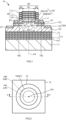
- FIG. 1 is a cross-sectional view of a Vertical Cavity Surface Emitting Laser (hereinafter referred to as a surface emitting laser: VCSEL) according to Embodiment 1.
- FIG. 2 is a schematic top view of a surface emitting laser 10.
- FIG. 1 is a cross-sectional view taken along the line V-V in FIG. 2 . The configuration of the surface emitting laser 10 will be described with reference to FIG. 1 and FIG. 2 .
- the surface emitting laser 10 includes a substrate 11 and a first multilayer film reflecting mirror (hereinafter simply referred to as a first reflecting mirror) 12 formed on the substrate 11.
- the first reflecting mirror 12 is formed on the substrate 11 and has a structure in which first semiconductor films (hereinafter referred to as high refractive index semiconductor films) H1 and second semiconductor films (hereinafter referred to as low refractive index semiconductor films) L1 having a refractive index lower than that of the high refractive index semiconductor film H1 are stacked in alternation.
- the first reflecting mirror 12 is a semiconductor multilayer film reflecting mirror constituting a Distributed Bragg Reflector (DBR) made of a semiconductor material.
- DBR Distributed Bragg Reflector
- the substrate 11 has a composition of GaN.
- the substrate 11 is a substrate for growth used for crystal growth of the first reflecting mirror 12.
- the high refractive index semiconductor layer H1 in the first reflecting mirror 12 has a composition of GaN, and the low refractive index semiconductor layer L1 has a composition of AlInN.
- a buffer layer (not illustrated) having a composition of GaN is disposed between the substrate 11 and the first reflecting mirror 12.
- the surface emitting laser 10 includes a light-emitting structure layer EM formed on the first reflecting mirror 12 and including a light-emitting layer 14.
- the light-emitting structure layer EM includes a plurality of semiconductor layers made of a nitride-based semiconductor.
- the light-emitting structure layer EM includes a n-type semiconductor layer (first semiconductor layer) 13 formed on the first reflecting mirror 12, the light-emitting layer (active layer) 14 formed on the n-type semiconductor layer 13, and a p-type semiconductor layer (second semiconductor layer) 15 formed on the light-emitting layer 14.
- the n-type semiconductor layer 13 has a composition of GaN and contains Si as n-type impurities.
- the light-emitting layer 14 has a quantum well structure that includes a well layer having a composition of InGaN and a barrier layer having a composition of GaN.
- a p-type semiconductor layer 15 has a GaN-based composition and contains Mg as p-type impurities.
- the configuration of the light-emitting structure layer EM is not limited to this.
- the n-type semiconductor layer 13 may include a plurality of n-type semiconductor layers having mutually different compositions.
- the p-type semiconductor layer 15 may include a plurality of p-type semiconductor layers having mutually different compositions.
- the p-type semiconductor layer 15 may include, for example, an AlGaN layer as an electron-blocking layer (not illustrated) that reduces an overflow of electrons injected into the light-emitting layer 14 to the p-type semiconductor layer 15 at the interface with the light-emitting layer 14.
- the p-type semiconductor layer 15 may include a contact layer (not illustrated) to form an ohmic contact with an electrode.
- the p-type semiconductor layer 15 only needs to include a GaN layer as a cladding layer between the electron-blocking layer and the contact layer.
- the p-type semiconductor layer 15 includes a first region 15A and a second region 15B in an upper surface 15U.
- the second region 15B is disposed outside the first region 15A and depressed from the first region 15A toward the light-emitting layer 14.
- the second region 15B includes an inactivated region 15C where p-type impurities are inactivated.
- the first region 15A projects from the second region 15B in a columnar shape.
- the first region 15A can be formed by performing dry etching on the upper surface 15U of the p-type semiconductor layer 15 with a circular region left.
- a surface of the semiconductor, such as the p-type semiconductor layer 15, containing impurities is roughened by dry etching. This inactivates the p-type impurities in the etched part, thus forming the inactivated region 15C.
- the second region 15B functions as a high resistance region HR having an electrical resistance higher than that of the first region 15A. Meanwhile, the region where etching is not performed, namely, the first region 15A, which is the region where the inactivated region 15C is not disposed, functions as a low resistance region LR. In the second region 15B, the p-type semiconductor layer 15 is partially removed by dry etching. Therefore, the second region 15B is depressed toward the light-emitting layer 14 side from the first region 15A.
- the p-type semiconductor layer 15 includes the low resistance region LR and the high resistance region HR in the upper surface 15U.
- the high resistance region HR is depressed from the low resistance region LR toward the light-emitting layer 14 outside the low resistance region LR.
- the p-type impurities are inactivated in the high resistance region HR such that the high resistance region HR has the electrical resistance higher than that of the low resistance region LR.
- the p-type semiconductor layer 15 functions as a current confinement layer that confines a current path from which a current is injected to the light-emitting structure layer EM.
- the first region 15A of the p-type semiconductor layer 15 functions as a current injected region from which a current is injected into the light-emitting layer 14.
- the second region 15B of the p-type semiconductor layer 15 functions as a non-current injected region from which the injection of a current into the light-emitting layer 14 is suppressed.
- the surface emitting laser 10 includes a light-transmitting electrode layer 16 in contact with the first and the second regions 15A and 15B of the p-type semiconductor layer 15 and formed on the upper surface 15U of the p-type semiconductor layer 15.
- the light-transmitting electrode layer 16 is a conductive film having translucency to light emitted from the light-emitting layer 14.
- the light-transmitting electrode layer 16 is made of a metal oxide film, such as ITO or IZO.
- the surface emitting laser 10 includes an insulating layer 17 formed on the light-transmitting electrode layer 16.
- the insulating layer 17 is made of a metal oxide, such as Ta 2 O 5 , Nb 2 O 5 , ZrO 2 , TiO 2 , and HfO 2 .
- the insulating layer 17 has translucency to the light emitted from the light-emitting layer 14.
- the surface emitting laser 10 includes a second multilayer film reflecting mirror (hereinafter simply referred to as a second reflecting mirror) 18 formed on the insulating layer 17.
- the second reflecting mirror 18 is disposed at a position facing the first reflecting film 12 via the light-emitting structure layer EM.
- a resonator OC having a direction perpendicular to the light-emitting structure layer EM (a direction perpendicular to the substrate 11) as a resonator length direction is constituted between the second reflecting mirror 18 and the first reflecting mirror 12.
- the second reflecting mirror 18 has a column shape. Therefore, in this embodiment, the surface emitting laser 10 includes the column-shaped resonator OC.
- the second reflecting mirror 18 has a structure in which first dielectric films (hereinafter referred to as high refractive index dielectric films) H2 and second dielectric films (hereinafter referred to as low refractive index dielectric films) L2 having a refractive index lower than that of the high refractive index dielectric films H2 are stacked in alternation.
- first dielectric films hereinafter referred to as high refractive index dielectric films
- second dielectric films hereinafter referred to as low refractive index dielectric films
- the second reflecting mirror 18 is a dielectric multilayer film reflecting mirror constituting a Distributed Bragg Reflector (DBR) made of a dielectric material.
- DBR Distributed Bragg Reflector
- the high refractive index dielectric film H2 is formed of a Ta 2 O 5 layer
- the low refractive index dielectric film L2 is made of an Al 2 O 3 layer.
- the low resistance region LR and the high resistance region HR of the p-type semiconductor layer 15 in the light-emitting structure layer EM are disposed in the region between the first reflecting mirror 12 and the second reflecting mirror 18. That is, in this embodiment, the resonator OC includes: a central region R1 corresponding to the low resistance region LR of the p-type semiconductor layer 15 and extending between the first and the second reflecting mirrors 12 and 18, and an outer region R2 disposed corresponding to the high resistance region HR outside the central region R1.
- a layer thickness of the p-type semiconductor layer 15 in the first region 15A is thicker (larger) than a layer thickness of the p-type semiconductor layer 15 in the second region 15B (high resistance region HR). Therefore, the outer region R2 in the resonator OC has an equivalent refractive index lower than that of the central region R1. That is, the central region R1 functions as a high refractive index region, and the outer region R2 functions as a low refractive index region having a refractive index lower than that of the central region R1.
- the central region R1 has a column shape
- the outer region R2 has a cylindrical shape.
- the surface emitting laser 10 includes first and second electrodes E1 and E2 that apply a current to the light-emitting structure layer EM.
- the first electrode E1 is formed on the n-type semiconductor layer 13.
- the second electrode E2 is formed on the light-transmitting electrode layer 16.
- the application of a voltage between the first and the second electrodes E1 and E2 emits the light from the light-emitting layer 14 in the light-emitting structure layer EM.
- the light emitted from the light-emitting layer 14 repeats reflection between the first and the second reflecting mirrors 12 and 18, thus entering a resonance state (performing laser oscillation).
- the first reflecting mirror 12 has reflectance slightly lower than that of the second reflecting mirror 18. Therefore, a part of the light resonated between the first and the second reflecting mirrors 12 and 18 transmits through the first reflecting mirror 12 and the substrate 11 and is taken to the outside.
- the surface emitting laser 10 emits the light in the direction perpendicular to the substrate 11 and the light-emitting structure layer EM.
- the first region 15A of the p-type semiconductor layer 15 defines a luminescence center in the light-emitting layer 14 and defines a center axis CA of the resonator OC.
- the center axis CA of the resonator OC passes through the center of the first region 15A and extends in the direction perpendicular to the p-type semiconductor layer 15 (light-emitting structure layer EM).
- the center of the first region 15A of the p-type semiconductor layer 15 is disposed at a position corresponding to the center of the second region 15B.
- the first reflecting mirror 12 is formed of 44 pairs of GaN layers and AlInN layers.
- the n-type semiconductor layer 13 has a layer thickness of 650 nm.
- the light-emitting layer 14 is formed of an active layer having a multiple quantum well structure in which 4 nm of InGaN layers and 5 nm of GaN layers are stacked three times.
- the second reflecting mirror 18 is formed of 10 pairs of Ta 2 O 5 layers and Al 2 O 3 layers.
- the p-type semiconductor layer 15 has a layer thickness of 50 nm in the first region 15A.
- the p-type semiconductor layer 15 has a layer thickness of 40 nm in the second region 15B.
- the first region 15A has a width (outer diameter) of 6 ⁇ m.
- FIG. 3 is a drawing schematically illustrating an optical property of the resonator OC in the surface emitting laser 10.
- FIG. 3 is a cross-sectional view similar to FIG. 1 , FIG. 3 omits hatchings.
- the layer thickness of the p-type semiconductor layer 15 in the first region 15A (low resistance region LR) is larger than the layer thickness of the p-type semiconductor layer 15 in the second region 15B (high resistance region HR).
- the layer thicknesses of the other layers between the first and the second reflecting mirrors 12 and 18 are each constant.
- an equivalent refractive index n1 of the central region R1 in the resonator OC is higher than an equivalent refractive index n2 of the outer region R2.
- an optical distance OL1 between the first and the second reflecting mirrors 12 and 18 in the central region R1 is larger than an optical distance OL2 in the outer region R2. That is, an equivalent resonator length in the central region R1 is longer than an equivalent resonator length in the outer region R2.
- FIG. 4 is a drawing schematically illustrating an electrical property in the resonator OC (in the light-emitting structure layer EM) of the surface emitting laser 10.
- FIG. 4 is a drawing schematically illustrating paths of currents CR flowing through the inside of the light-emitting structure layer EM.
- FIG. 4 is a cross-sectional view similar to FIG. 1 , FIG. 4 omits hatchings.
- the central region R1 corresponding to the first region 15A functions as the low resistance region LR
- the outer region R2 corresponding to the second region 15B functions as the high resistance region HR.
- the current CR is injected into the light-emitting layer 14 only in the central region R1, and the current is hardly injected into the light-emitting layer 14 in the outer region R2. That is, while light is generated (a gain is generated) in the central region R1, light is not generated in the outer region R2.
- FIG. 5 is a drawing schematically illustrating light emitted from the surface emitting laser 10.
- a standing wave in the surface emitting laser 10 is taken to the outside from the first reflecting mirror 12.
- light resonated in the surface emitting laser 10 is taken to the outside while being converged at the central region R1.
- FIG. 5 schematically illustrates a beam outer edge of a laser beam LB emitted from the surface emitting laser 10 by the dashed line.
- the equivalent refractive index n2 of the resonator OC (laser medium) in the outer region R2 is smaller than the equivalent refractive index n1 of the resonator OC in the central region R1.
- the low resistance region LR that is, the current injected region to the light-emitting layer 14 is restricted to only the central region R1. That is, the current is not injected into the outer region R2, but the current injected region is disposed surrounding the non-current injected region. This allows stabilizing a transverse mode of the laser beam LB. For example, this allows emitting the unimodal laser beam LB.
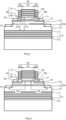
- FIG. 6 is a cross-sectional view of a surface emitting laser 100 according to Comparative Example 1. Except that the surface emitting laser 100 includes an insulating layer 101 on the second region 15B, the surface emitting laser 100 has a configuration similar to that of the surface emitting laser 10.
- the p-type semiconductor layer 15 contacts the insulating layer 101 in the second region 15B.
- the p-type semiconductor layer 15 contacts the light-transmitting electrode layer 16 in the first region 15A.
- the insulating layer 101 is made of SiO 2 .
- FIG. 7 is a drawing illustrating a relationship between etching depths at the upper surfaces 15U of the p-type semiconductor layers 15 in the surface emitting laser 10 and the surface emitting laser 100, that is, distances between the first and the second regions 15A and 15B in a direction perpendicular to the p-type semiconductor layers 15 (correspond to a depth D1 in the surface emitting laser 10 and a depth D2 in the surface emitting laser 100, see FIG. 1 and FIG.
- refractive index differences ⁇ n which are values found by dividing the differences in the equivalent refractive indexes between the central regions R1 and the outer regions R2 of both by the equivalent refractive indexes of the central regions R1 (the values correspond to (n1 - n2)/n1 in the surface emitting laser 10 and (n11 - n21)/n11 in the surface emitting laser 100, see FIG. 1 and FIG. 6 , respectively).
- FIG. 7 shows simulation results in a case where resonator lengths (corresponding to the optical distances OL1 and OL11, respectively, see FIG. 1 and FIG. 6 ) in both of the surface emitting lasers 10 and 100 are set to be five times or 10 times of a wavelength of the light (that is, the laser beam LB) emitted from the light-emitting layer 14.
- the p-type semiconductor layer 15 needs to be etched such that the second region 15B becomes lower than the first region 15A by the depth D2, which is about 22 nm.
- the refractive index difference ⁇ n of 3 ⁇ 10 -3 can be obtained by etching of only by the depth D1, which is about 5 nm. It is seen that the sufficient refractive index difference can also be formed by decreasing the etching depth D1 in all the other range in the surface emitting laser 10.
- the sufficient refractive index difference can be formed in the resonator OC compared with a case where, for example, the p-type semiconductor layer 15 is partially removed and then the insulating layer 101 is formed to form the refractive index difference in the resonator OC as in the surface emitting laser 100.
- an amount of the removed p-type semiconductor layer 15 (for example, an amount of etching and an etching period) is substantially reduced. This shortens the manufacturing period of the surface emitting laser 10.
- the light-transmitting electrode layer 16 is formed on the first and the second regions 15A and 15B, for example, a step difference occurs in each layer from the light-transmitting electrode layer 16 to the second reflecting mirror 18 at the boundary between the central region R1 and the outer region R2.
- the step difference is slight (for example, 10 nm or less). Therefore, a scattering loss of the laser beam LB that possibly occurs due to the step difference in each layer is almost negligible.
- the step height (etching depth) D1 between the first and the second regions 15A and 15B is preferably, for example, 9.2 nm or less, and 4.7 nm or less is further preferred. This is because the step difference in the height range is insensitive to the laser beam LB. This embodiment eliminates the need for the insulating layer 101, thereby allowing forming a desired refractive index difference while achieving the range of the etching depth D 1.
- the preferred ranges of the resonator length of the central region R1 and the refractive index difference between the central region R1 and the outer region R2 formed in the resonator OC may be determined, and the depth D1 of the second region 15B may be adjusted to meet the ranges.
- the refractive index difference is preferably provided between the central region R1 and the outer region R2 in a range of 1 ⁇ 10 -3 to 4 ⁇ 10 -3 .
- the depth D1 of the first region 15A is preferably in a range of from 1.5 to 12 nm. That is, the high resistance region HR is preferably depressed from the low resistance region LR toward the light-emitting layer 14 at the depth in of range of from 1.5 to 12 nm.
- FIG. 8 is a drawing illustrating the far-field patterns and their properties of the laser beam LB emitted from the surface emitting laser 10 when respective driving conditions are adjusted.
- FIG. 8 shows measurement results when the width W1 (the width of the low resistance region LR and corresponding to the inner diameter in this embodiment, see FIG. 1 ) of the second region 15B is set to 6 ⁇ m, the resonator length OL1 is set to 10 times of a peak wavelength ⁇ (445 nm in this embodiment) of the laser beam LB, and the refractive index difference ⁇ n between the central region R1 and the outer region R2 is set to 1.5 ⁇ 10 -3 .
- the unimodal far-field pattern was able to be obtained and its half-value angle was 6° or less. That is, it is seen that, in the operation under various driving conditions as well, the stable, unimodal laser beam LB can be emitted. Thus, it is seen that the surface emitting laser 10 can emit the laser beam LB in the stable transverse mode.
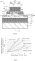
- FIG. 9 is a drawing illustrating a relationship between the driving period and the optical output in the surface emitting lasers 10 and 100.
- FIG. 9 is a drawing illustrating the relationship between the driving period and the optical output of the surface emitting lasers 10 and 100 with the optical output at the start of the driving set to 1.
- the reduction in optical output is suppressed in the surface emitting laser 10 compared with the surface emitting laser 100. That is, it is seen that the surface emitting laser 10 features the stable output characteristics and high quality compared with the surface emitting laser 100.
- the surface emitting laser 10 not including the insulating layer 101, which is disposed in the surface emitting laser 100.
- the p-type semiconductor layer 15 semiconductor wafer
- the insulating layer 101 is formed by the p-type semiconductor layer 15 (semiconductor wafer) and stress is applied to the p-type semiconductor layer 15.
- damage given to the p-type semiconductor layer 15 is eliminated. Accordingly, it is considered that the surface emitting laser 10 maintaining the p-type semiconductor layer 15 in the high quality state can be obtained and the output characteristics are stabilized.
- the inactivated region 15C is disposed on the upper surface 15U of the p-type semiconductor layer 15 in the surface emitting laser 10, and thus the second region 15B that functions as the high resistance region HR is provided. Therefore, the laser beam LB in the high quality, stable transverse mode with high output power can be emitted.
- the high resistance region HR and the low resistance region LR are disposed in the p-type semiconductor layer 15 has been described.
- the high resistance region HR and the low resistance region LR may be disposed in the n-type semiconductor layer 13.
- the high resistance region HR is formed by dry etching.
- the method for forming the high resistance region HR is not limited to dry etching.
- the second region 15B in the p-type semiconductor layer 15 may be formed by slightly removing the surface of the p-type semiconductor layer 15 and ion implantation is performed to form the inactivated region 15C.
- the inactivated region 15C may be formed by ashing process.
- FIG. 10 is a cross-sectional view of a surface emitting laser 10A according to modification of this embodiment. Except that the surface emitting laser 10A includes an insulating layer 19 on an outer peripheral portion of the first region 15A of the p-type semiconductor layer 15 between the p-type semiconductor layer 15 and the light-transmitting electrode layer 16, the surface emitting laser 10A has a configuration similar to that of the surface emitting laser 10.
- the insulating layer 19 is formed on the outer peripheral portion of the second region 15B of the p-type semiconductor layer 15 having a region immediately below the second electrode E2, and the light-transmitting electrode layer 16 is formed so as to embed the insulating layer 19.
- partially forming the insulating layer 19 allows reliable insulation between the second region 15B and the light-transmitting electrode layer 16 while minimally suppressing damage to the p-type semiconductor layer 15. This allows reliably setting the second region 15B in the high resistance. Accordingly, a decrease in gain due to, for example, a leakage of a current in the second region 15B can be suppressed.
- the surface emitting laser 10A that emits the laser beam LB in that stable, high quality transverse mode with high output power is obtained.
- the surface emitting laser 10 includes the substrate 11, the first reflecting mirror 12, the n-type semiconductor layer (the first semiconductor layer having a first conductivity type) 13, the light-emitting layer 14, the p-type semiconductor layer (second semiconductor layer) 15, the light-transmitting electrode layer 16, and the second reflecting mirror 18.
- the first reflecting mirror 12 is formed on the substrate 11.
- the n-type semiconductor layer 13 is formed on the first reflecting mirror 12.
- the light-emitting layer 14 is formed on the n-type semiconductor layer 13.
- the p-type semiconductor layer 15 is formed on the light-emitting layer 14 and has a p-type conductivity type (second conductivity type) opposite to the first conductivity type of the n-type semiconductor layer 13.
- the p-type semiconductor layer 15 includes the low resistance region LR and the high resistance region HR on the upper surface 15U.
- the high resistance region HR is depressed from the low resistance region LR toward the light-emitting layer 14 outside the low resistance region LR and p-type impurities are inactivated in the high resistance region HR such that the high resistance region HR has the electrical resistance higher than the electrical resistance of the low resistance region LR.
- the light-transmitting electrode layer 16 in contact with the low resistance region LR and the high resistance region HR is formed on the upper surface 15U of the p-type semiconductor layer 15.
- the second reflecting mirror 18 is formed on the light-transmitting electrode layer 16.
- the resonator OC is constituted between the second reflecting mirror 18 and the first reflecting mirror 12. This allows emitting the light in the stable transverse mode and therefore allows providing the high quality surface emitting laser 10 (vertical cavity surface emitting device) having the simple configuration.
- FIG. 11 is a cross-sectional view of a surface emitting laser 20 according to Embodiment 2.
- FIG. 12 is a schematic top view of the surface emitting laser 20. Except for a configuration of a light-emitting structure layer EM1, the surface emitting laser 20 has a configuration similar to that of the surface emitting laser 10.
- the light-emitting structure layer EM1 includes a p-type semiconductor layer 21 that includes the high resistance region HR inside the low resistance region LR on an upper surface 21U.
- the low resistance region LR is disposed in a ring shape and the high resistance regions HR are disposed in both the inside and the outside of the low resistance region LR.
- the p-type semiconductor layer 21 includes a first region 21A disposed in the ring shape on an upper surface 21U and functioning as the low resistance region LR, a second region 21B1 depressed from the first region 21A toward the light-emitting layer 14 at the inside of the first region 21A and functioning as the high resistance region HR, and a third region 21B2 depressed from the first region 21A toward the light-emitting layer 14 at the outside of the first region 21A and functioning as the high resistance region HR.
- the p-type semiconductor layer 21 can be formed by performing dry etching on the surface of the p-type semiconductor layer 21 with the ring-shaped region left.
- the ring-shaped region as the first region 21A has an outer diameter of 10.3 ⁇ m and an inner diameter of 3.5 ⁇ m.
- a resonator OC1 includes a ring-shaped region R11 corresponding to the first region 21A, an inner region R21 corresponding to the second region 21B1 disposed inside the ring-shaped region R11, and an outer region R22 corresponding to the third region 21B2 disposed outside the ring-shaped region R11.
- the inner region R21 and the outer region R22 have equivalent refractive indexes lower than that of the ring-shaped region R11.
- the inner region R21 is formed in a columnar shape, and the ring-shaped region R11 and the outer region R22 are formed in a cylindrical shape.
- a current flows only through the ring-shaped region R11.
- the current confinement is performed on the resonator OC1 by thus disposing the inner region R21 to ensure stabilizing an eigenmode (also referred to as a supermode) of the laser beam LB.
- eigenmode also referred to as a supermode
- adjustment of the width (a width of the first region 21A corresponding to the width of the current injected region) of the ring-shaped region R11 allows stably generating the laser beam LB in various eigenmodes.
- the p-type semiconductor layer 21 includes the high resistance region HR in which an inactivated region 21C is formed inside the low resistance region LR. This allows emitting the light in the stable transverse mode and therefore allows providing the high quality surface emitting laser 20 (vertical cavity surface emitting device) having the simple configuration.
Landscapes
- Physics & Mathematics (AREA)
- Condensed Matter Physics & Semiconductors (AREA)
- General Physics & Mathematics (AREA)
- Electromagnetism (AREA)
- Optics & Photonics (AREA)
- Semiconductor Lasers (AREA)
Applications Claiming Priority (2)
| Application Number | Priority Date | Filing Date | Title |
|---|---|---|---|
| JP2018196394A JP7166871B2 (ja) | 2018-10-18 | 2018-10-18 | 垂直共振器型発光素子 |
| PCT/JP2019/039456 WO2020080161A1 (ja) | 2018-10-18 | 2019-10-07 | 垂直共振器型発光素子 |
Publications (3)
| Publication Number | Publication Date |
|---|---|
| EP3869642A1 EP3869642A1 (en) | 2021-08-25 |
| EP3869642A4 EP3869642A4 (en) | 2022-07-20 |
| EP3869642B1 true EP3869642B1 (en) | 2024-03-06 |
Family
ID=70284329
Family Applications (1)
| Application Number | Title | Priority Date | Filing Date |
|---|---|---|---|
| EP19872622.6A Active EP3869642B1 (en) | 2018-10-18 | 2019-10-07 | Vertical resonator-type light-emitting element |
Country Status (5)
| Country | Link |
|---|---|
| US (2) | US12218486B2 (enExample) |
| EP (1) | EP3869642B1 (enExample) |
| JP (1) | JP7166871B2 (enExample) |
| CN (1) | CN112913093B (enExample) |
| WO (1) | WO2020080161A1 (enExample) |
Families Citing this family (8)
| Publication number | Priority date | Publication date | Assignee | Title |
|---|---|---|---|---|
| JP7166871B2 (ja) | 2018-10-18 | 2022-11-08 | スタンレー電気株式会社 | 垂直共振器型発光素子 |
| JP7190865B2 (ja) * | 2018-10-18 | 2022-12-16 | スタンレー電気株式会社 | 垂直共振器型発光素子 |
| JP7227469B2 (ja) * | 2019-01-29 | 2023-02-22 | 日亜化学工業株式会社 | 垂直共振器面発光レーザ素子 |
| JP7288360B2 (ja) | 2019-07-01 | 2023-06-07 | スタンレー電気株式会社 | 垂直共振器型発光素子 |
| JP7523258B2 (ja) * | 2020-06-12 | 2024-07-26 | スタンレー電気株式会社 | 垂直共振器型発光素子 |
| JP7623563B2 (ja) * | 2020-07-27 | 2025-01-29 | 日亜化学工業株式会社 | 垂直共振器面発光レーザ素子 |
| DE112022002708T5 (de) * | 2021-05-21 | 2024-03-07 | Ams-Osram International Gmbh | Verfahren zur herstellung eines halbleiterbauelements und halbleiterbauelement |
| WO2025131591A1 (en) * | 2023-12-21 | 2025-06-26 | Ams-Osram International Gmbh | OPTICAL APERTURES FOR InGaN VCSEL |
Family Cites Families (82)
| Publication number | Priority date | Publication date | Assignee | Title |
|---|---|---|---|---|
| JPS53140883A (en) | 1977-05-16 | 1978-12-08 | Terumo Corp | Urinary output monitor |
| US5058120A (en) * | 1990-02-28 | 1991-10-15 | Kabushiki Kaisha Toshiba | Visible light emitting semiconductor laser with inverse mesa-shaped groove section |
| JP3395194B2 (ja) | 1990-09-12 | 2003-04-07 | セイコーエプソン株式会社 | 面発光型半導体レーザ |
| US5625637A (en) | 1991-03-28 | 1997-04-29 | Seiko Epson Corporation | Surface emitting semiconductor laser and its manufacturing process |
| US5594751A (en) * | 1995-06-26 | 1997-01-14 | Optical Concepts, Inc. | Current-apertured vertical cavity laser |
| JPH0918084A (ja) | 1995-06-26 | 1997-01-17 | Seiko Epson Corp | 面発光型半導体レーザ及びその製造方法 |
| EP0852416B1 (en) | 1995-09-18 | 2002-07-10 | Hitachi, Ltd. | Semiconductor material, method of producing the semiconductor material, and semiconductor device |
| JPH11121864A (ja) | 1997-10-08 | 1999-04-30 | Seiko Epson Corp | 面発光レーザ及びその製造方法 |
| US5915165A (en) | 1997-12-15 | 1999-06-22 | Xerox Corporation | Method of manufacturing vertical cavity surface emitting semiconductor lasers using intermixing and oxidation |
| JP2000196189A (ja) * | 1998-12-24 | 2000-07-14 | Toshiba Corp | 面発光型半導体レーザ |
| US6376269B1 (en) | 1999-02-02 | 2002-04-23 | Agilent Technologies, Inc. | Vertical cavity surface emitting laser (VCSEL) using buried Bragg reflectors and method for producing same |
| JP2000299492A (ja) | 1999-04-15 | 2000-10-24 | Daido Steel Co Ltd | 量子井戸型発光ダイオード |
| US6751245B1 (en) * | 1999-06-02 | 2004-06-15 | Optical Communication Products, Inc. | Single mode vertical cavity surface emitting laser |
| US6507595B1 (en) | 1999-11-22 | 2003-01-14 | Avalon Photonics | Vertical-cavity surface-emitting laser comprised of single laser elements arranged on a common substrate |
| US6396865B1 (en) | 2000-10-27 | 2002-05-28 | Wisconsin Alumni Research Foundation | Vertical-cavity surface-emitting lasers with antiresonant reflecting optical waveguides |
| KR100384598B1 (ko) | 2000-11-29 | 2003-05-22 | 주식회사 옵토웰 | 질화물반도체 수직공진 표면발광 레이저 |
| KR100345452B1 (ko) * | 2000-12-14 | 2002-07-26 | 한국전자통신연구원 | 상부거울층 양단부에 확산영역을 구비하는 장파장표면방출 레이저 소자 및 그 제조 방법 |
| US6546029B2 (en) * | 2001-03-15 | 2003-04-08 | Ecole Polytechnique Federale De Lausanne | Micro-electromechanically tunable vertical cavity photonic device and a method of fabrication thereof |
| US6589805B2 (en) * | 2001-03-26 | 2003-07-08 | Gazillion Bits, Inc. | Current confinement structure for vertical cavity surface emitting laser |
| JP2003163373A (ja) * | 2001-11-26 | 2003-06-06 | Toyoda Gosei Co Ltd | Iii族窒化物系化合物半導体発光素子 |
| AU2003256382A1 (en) | 2002-07-06 | 2004-01-23 | Optical Communication Products, Inc. | Method of self-aligning an oxide aperture with an annular intra-cavity contact in a long wavelength vcsel |
| JP3857632B2 (ja) | 2002-09-27 | 2006-12-13 | 株式会社東芝 | 垂直共振器型面発光レーザ素子 |
| US20040179566A1 (en) * | 2003-03-11 | 2004-09-16 | Aharon El-Bahar | Multi-color stacked semiconductor lasers |
| JP2004288674A (ja) | 2003-03-19 | 2004-10-14 | Fuji Xerox Co Ltd | 面発光型半導体レーザおよびそれを用いた光通信システム |
| JP4641736B2 (ja) | 2003-10-28 | 2011-03-02 | ソニー株式会社 | 面発光半導体レーザーとその製造方法及び光学装置 |
| US7542499B2 (en) | 2003-11-27 | 2009-06-02 | Ricoh Company, Ltd. | Surface-emission laser diode and surface-emission laser array, optical interconnection system, optical communication system, electrophotographic system, and optical disk system |
| JP2005197426A (ja) * | 2004-01-07 | 2005-07-21 | Yokogawa Electric Corp | 面発光レーザ |
| JP4602685B2 (ja) | 2004-04-14 | 2010-12-22 | 株式会社リコー | 垂直共振器型面発光半導体レーザ素子および発光装置および光伝送システム |
| JP4602692B2 (ja) | 2004-04-23 | 2010-12-22 | 株式会社リコー | 面発光レーザ及び光伝送システム |
| US20190245318A1 (en) | 2004-10-29 | 2019-08-08 | Ronald LaComb | Concentric Cylindrical Circumferential Laser |
| WO2006056208A2 (en) | 2004-11-29 | 2006-06-01 | Alight Technologies A/S | Single-mode photonic-crystal vcsels |
| JP2006245379A (ja) | 2005-03-04 | 2006-09-14 | Stanley Electric Co Ltd | 半導体発光素子 |
| US20070025407A1 (en) * | 2005-07-29 | 2007-02-01 | Koelle Bernhard U | Long-wavelength VCSEL system with heat sink |
| JP4548329B2 (ja) | 2005-12-19 | 2010-09-22 | セイコーエプソン株式会社 | 面発光型半導体レーザ |
| JP4548345B2 (ja) | 2006-01-12 | 2010-09-22 | セイコーエプソン株式会社 | 面発光型半導体レーザ |
| JPWO2007116659A1 (ja) | 2006-03-23 | 2009-08-20 | 日本電気株式会社 | 面発光レーザ |
| JP5082344B2 (ja) | 2006-08-31 | 2012-11-28 | 富士ゼロックス株式会社 | 面発光型半導体レーザおよびその製造方法 |
| JP5228363B2 (ja) | 2007-04-18 | 2013-07-03 | ソニー株式会社 | 発光素子 |
| JP2009038310A (ja) | 2007-08-03 | 2009-02-19 | Sumitomo Electric Ind Ltd | 面発光型半導体光デバイス |
| JP2009170508A (ja) | 2008-01-11 | 2009-07-30 | Furukawa Electric Co Ltd:The | 面発光半導体レーザ及びその製造方法 |
| JP4479804B2 (ja) * | 2008-02-13 | 2010-06-09 | 富士ゼロックス株式会社 | 面発光型半導体レーザ |
| WO2009119172A1 (ja) | 2008-03-28 | 2009-10-01 | 日本電気株式会社 | 面発光レーザ |
| JP5006242B2 (ja) | 2008-03-31 | 2012-08-22 | 古河電気工業株式会社 | 面発光半導体レーザ素子 |
| US8030666B2 (en) * | 2008-04-16 | 2011-10-04 | Taiwan Semiconductor Manufacturing Company, Ltd. | Group-III nitride epitaxial layer on silicon substrate |
| JP2009266919A (ja) | 2008-04-23 | 2009-11-12 | Sony Corp | 面発光型半導体レーザおよびその製造方法 |
| GB0817786D0 (en) | 2008-09-30 | 2008-11-05 | Bookham Technology Plc | Improved vertical cavity surface emitting laser |
| JP5521478B2 (ja) * | 2008-10-22 | 2014-06-11 | 日亜化学工業株式会社 | 窒化物半導体発光素子の製造方法及び窒化物半導体発光素子 |
| JP2010114214A (ja) * | 2008-11-05 | 2010-05-20 | Fuji Xerox Co Ltd | 面発光型半導体レーザ素子、面発光型半導体レーザ素子の製造方法、および光送信装置 |
| JP5435503B2 (ja) * | 2008-12-10 | 2014-03-05 | 古河電気工業株式会社 | 半導体レーザ素子およびその製造方法 |
| JP2012517705A (ja) * | 2009-02-11 | 2012-08-02 | ダンマークス テクニスク ユニバーシテット | ハイブリッド垂直キャビティレーザー |
| JP5707742B2 (ja) | 2009-06-30 | 2015-04-30 | 日亜化学工業株式会社 | 垂直共振器型面発光レーザ |
| JP4934705B2 (ja) * | 2009-07-28 | 2012-05-16 | キヤノン株式会社 | 面発光レーザ、面発光レーザの製造方法、画像形成装置 |
| JP5460412B2 (ja) * | 2010-03-26 | 2014-04-02 | 古河電気工業株式会社 | 半導体レーザ素子およびその製造方法 |
| JP5754624B2 (ja) * | 2010-05-25 | 2015-07-29 | 株式会社リコー | 面発光レーザ素子、面発光レーザアレイ、光走査装置、画像形成装置及び面発光レーザ素子の製造方法 |
| JP5633435B2 (ja) * | 2011-03-09 | 2014-12-03 | 日亜化学工業株式会社 | 面発光レーザ素子 |
| EP2533380B8 (en) | 2011-06-06 | 2017-08-30 | Mellanox Technologies, Ltd. | High speed lasing device |
| US8731012B2 (en) | 2012-01-24 | 2014-05-20 | Fuji Xerox Co., Ltd. | Surface emitting semiconductor laser and its manufacturing method, surface emitting semiconductor laser device, optical transmitter, and information processor |
| WO2014018943A1 (en) | 2012-07-27 | 2014-01-30 | Thorlabs, Inc. | Mems-tunable short cavity laser |
| JP6240429B2 (ja) * | 2013-08-07 | 2017-11-29 | 国立大学法人東京工業大学 | 面発光型半導体レーザおよび光伝送装置 |
| US20170093128A1 (en) * | 2014-03-04 | 2017-03-30 | Hewlett Packard Enterprise Development Lp | Vertical-cavity surface-emitting lasers |
| US11095096B2 (en) * | 2014-04-16 | 2021-08-17 | Yale University | Method for a GaN vertical microcavity surface emitting laser (VCSEL) |
| DE112016003410T5 (de) * | 2015-07-28 | 2018-04-26 | Sony Corporation | Lichtemittierendes Element |
| JP6664688B2 (ja) * | 2015-11-19 | 2020-03-13 | 学校法人 名城大学 | 垂直共振器型発光素子 |
| JP6700027B2 (ja) | 2015-11-20 | 2020-05-27 | スタンレー電気株式会社 | 垂直共振器型発光素子 |
| JP6990499B2 (ja) | 2016-04-18 | 2022-01-12 | スタンレー電気株式会社 | 垂直共振器型発光素子及び垂直共振型発光素子の製造方法 |
| JP2018073853A (ja) * | 2016-10-24 | 2018-05-10 | スタンレー電気株式会社 | 反射鏡、垂直共振器型発光装置及びその製造方法 |
| US10873174B2 (en) | 2016-11-02 | 2020-12-22 | Sony Corporation | Light-emitting element and method of manufacturing the same |
| JP6966843B2 (ja) | 2017-02-08 | 2021-11-17 | スタンレー電気株式会社 | 垂直共振器型発光素子 |
| JP6932345B2 (ja) * | 2017-03-27 | 2021-09-08 | 学校法人 名城大学 | 半導体多層膜反射鏡及び垂直共振器型発光素子 |
| CN106848838B (zh) | 2017-04-06 | 2019-11-29 | 中国科学院半导体研究所 | 基于多孔DBR的GaN基VCSEL芯片及制备方法 |
| US10681474B2 (en) * | 2017-09-19 | 2020-06-09 | Vocalzoom Systems Ltd. | Laser-based devices utilizing improved self-mix sensing |
| JP7039905B2 (ja) * | 2017-09-21 | 2022-03-23 | 富士フイルムビジネスイノベーション株式会社 | 発光部品の製造方法 |
| JP6369613B1 (ja) * | 2017-09-21 | 2018-08-08 | 富士ゼロックス株式会社 | 発光部品、プリントヘッド及び画像形成装置 |
| EP3496216A1 (en) | 2017-12-08 | 2019-06-12 | Koninklijke Philips N.V. | Segmented vertical cavity surface emitting laser |
| US10892601B2 (en) | 2018-05-24 | 2021-01-12 | Stanley Electric Co., Ltd. | Vertical cavity light-emitting element |
| JP7212882B2 (ja) | 2018-05-24 | 2023-01-26 | スタンレー電気株式会社 | 垂直共振器型発光素子 |
| JP7190865B2 (ja) | 2018-10-18 | 2022-12-16 | スタンレー電気株式会社 | 垂直共振器型発光素子 |
| JP7166871B2 (ja) | 2018-10-18 | 2022-11-08 | スタンレー電気株式会社 | 垂直共振器型発光素子 |
| JP7258591B2 (ja) | 2019-02-21 | 2023-04-17 | スタンレー電気株式会社 | 垂直共振器型発光素子 |
| JP7291497B2 (ja) | 2019-02-21 | 2023-06-15 | スタンレー電気株式会社 | 垂直共振器型発光素子 |
| JP7288360B2 (ja) | 2019-07-01 | 2023-06-07 | スタンレー電気株式会社 | 垂直共振器型発光素子 |
| WO2022185766A1 (ja) | 2021-03-03 | 2022-09-09 | ソニーグループ株式会社 | 面発光レーザ及び面発光レーザの製造方法 |
-
2018
- 2018-10-18 JP JP2018196394A patent/JP7166871B2/ja active Active
-
2019
- 2019-10-07 CN CN201980068567.3A patent/CN112913093B/zh active Active
- 2019-10-07 WO PCT/JP2019/039456 patent/WO2020080161A1/ja not_active Ceased
- 2019-10-07 US US17/285,635 patent/US12218486B2/en active Active
- 2019-10-07 EP EP19872622.6A patent/EP3869642B1/en active Active
-
2024
- 2024-12-31 US US19/006,794 patent/US20250158360A1/en active Pending
Also Published As
| Publication number | Publication date |
|---|---|
| JP2020064994A (ja) | 2020-04-23 |
| EP3869642A1 (en) | 2021-08-25 |
| CN112913093A (zh) | 2021-06-04 |
| JP7166871B2 (ja) | 2022-11-08 |
| EP3869642A4 (en) | 2022-07-20 |
| CN112913093B (zh) | 2024-09-13 |
| US12218486B2 (en) | 2025-02-04 |
| US20250158360A1 (en) | 2025-05-15 |
| WO2020080161A1 (ja) | 2020-04-23 |
| US20210384706A1 (en) | 2021-12-09 |
Similar Documents
| Publication | Publication Date | Title |
|---|---|---|
| EP3869642B1 (en) | Vertical resonator-type light-emitting element | |
| EP3930122B1 (en) | Vertical resonator-type light-emitting device | |
| JP7586446B2 (ja) | 垂直共振器型発光素子 | |
| JP7212882B2 (ja) | 垂直共振器型発光素子 | |
| EP3869643B1 (en) | Vertical resonator-type light-emitting element | |
| US12272927B2 (en) | Vertical cavity surface emitting device | |
| US12266906B2 (en) | Vertical cavity surface emitting device | |
| EP4089860A1 (en) | Vertical-resonator-type light-emitting element | |
| JP7406365B2 (ja) | 垂直共振器型発光素子 |
Legal Events
| Date | Code | Title | Description |
|---|---|---|---|
| STAA | Information on the status of an ep patent application or granted ep patent |
Free format text: STATUS: THE INTERNATIONAL PUBLICATION HAS BEEN MADE |
|
| PUAI | Public reference made under article 153(3) epc to a published international application that has entered the european phase |
Free format text: ORIGINAL CODE: 0009012 |
|
| STAA | Information on the status of an ep patent application or granted ep patent |
Free format text: STATUS: REQUEST FOR EXAMINATION WAS MADE |
|
| 17P | Request for examination filed |
Effective date: 20210416 |
|
| AK | Designated contracting states |
Kind code of ref document: A1 Designated state(s): AL AT BE BG CH CY CZ DE DK EE ES FI FR GB GR HR HU IE IS IT LI LT LU LV MC MK MT NL NO PL PT RO RS SE SI SK SM TR |
|
| DAV | Request for validation of the european patent (deleted) | ||
| DAX | Request for extension of the european patent (deleted) | ||
| A4 | Supplementary search report drawn up and despatched |
Effective date: 20220622 |
|
| RIC1 | Information provided on ipc code assigned before grant |
Ipc: H01S 5/343 20060101ALN20220615BHEP Ipc: H01S 5/20 20060101ALN20220615BHEP Ipc: H01S 5/042 20060101ALI20220615BHEP Ipc: H01S 5/183 20060101AFI20220615BHEP |
|
| RIC1 | Information provided on ipc code assigned before grant |
Ipc: H01S 5/343 20060101ALN20230704BHEP Ipc: H01S 5/20 20060101ALN20230704BHEP Ipc: H01S 5/042 20060101ALI20230704BHEP Ipc: H01S 5/183 20060101AFI20230704BHEP |
|
| RIC1 | Information provided on ipc code assigned before grant |
Ipc: H01S 5/343 20060101ALN20230816BHEP Ipc: H01S 5/20 20060101ALN20230816BHEP Ipc: H01S 5/042 20060101ALI20230816BHEP Ipc: H01S 5/183 20060101AFI20230816BHEP |
|
| GRAP | Despatch of communication of intention to grant a patent |
Free format text: ORIGINAL CODE: EPIDOSNIGR1 |
|
| STAA | Information on the status of an ep patent application or granted ep patent |
Free format text: STATUS: GRANT OF PATENT IS INTENDED |
|
| INTG | Intention to grant announced |
Effective date: 20231004 |
|
| GRAS | Grant fee paid |
Free format text: ORIGINAL CODE: EPIDOSNIGR3 |
|
| GRAA | (expected) grant |
Free format text: ORIGINAL CODE: 0009210 |
|
| STAA | Information on the status of an ep patent application or granted ep patent |
Free format text: STATUS: THE PATENT HAS BEEN GRANTED |
|
| AK | Designated contracting states |
Kind code of ref document: B1 Designated state(s): AL AT BE BG CH CY CZ DE DK EE ES FI FR GB GR HR HU IE IS IT LI LT LU LV MC MK MT NL NO PL PT RO RS SE SI SK SM TR |
|
| REG | Reference to a national code |
Ref country code: CH Ref legal event code: EP |
|
| REG | Reference to a national code |
Ref country code: IE Ref legal event code: FG4D |
|
| REG | Reference to a national code |
Ref country code: DE Ref legal event code: R096 Ref document number: 602019047994 Country of ref document: DE |
|
| REG | Reference to a national code |
Ref country code: LT Ref legal event code: MG9D |
|
| PG25 | Lapsed in a contracting state [announced via postgrant information from national office to epo] |
Ref country code: LT Free format text: LAPSE BECAUSE OF FAILURE TO SUBMIT A TRANSLATION OF THE DESCRIPTION OR TO PAY THE FEE WITHIN THE PRESCRIBED TIME-LIMIT Effective date: 20240306 |
|
| REG | Reference to a national code |
Ref country code: NL Ref legal event code: MP Effective date: 20240306 |
|
| PG25 | Lapsed in a contracting state [announced via postgrant information from national office to epo] |
Ref country code: GR Free format text: LAPSE BECAUSE OF FAILURE TO SUBMIT A TRANSLATION OF THE DESCRIPTION OR TO PAY THE FEE WITHIN THE PRESCRIBED TIME-LIMIT Effective date: 20240607 |
|
| PG25 | Lapsed in a contracting state [announced via postgrant information from national office to epo] |
Ref country code: HR Free format text: LAPSE BECAUSE OF FAILURE TO SUBMIT A TRANSLATION OF THE DESCRIPTION OR TO PAY THE FEE WITHIN THE PRESCRIBED TIME-LIMIT Effective date: 20240306 Ref country code: RS Free format text: LAPSE BECAUSE OF FAILURE TO SUBMIT A TRANSLATION OF THE DESCRIPTION OR TO PAY THE FEE WITHIN THE PRESCRIBED TIME-LIMIT Effective date: 20240606 |
|
| PG25 | Lapsed in a contracting state [announced via postgrant information from national office to epo] |
Ref country code: ES Free format text: LAPSE BECAUSE OF FAILURE TO SUBMIT A TRANSLATION OF THE DESCRIPTION OR TO PAY THE FEE WITHIN THE PRESCRIBED TIME-LIMIT Effective date: 20240306 |
|
| PG25 | Lapsed in a contracting state [announced via postgrant information from national office to epo] |
Ref country code: RS Free format text: LAPSE BECAUSE OF FAILURE TO SUBMIT A TRANSLATION OF THE DESCRIPTION OR TO PAY THE FEE WITHIN THE PRESCRIBED TIME-LIMIT Effective date: 20240606 Ref country code: NO Free format text: LAPSE BECAUSE OF FAILURE TO SUBMIT A TRANSLATION OF THE DESCRIPTION OR TO PAY THE FEE WITHIN THE PRESCRIBED TIME-LIMIT Effective date: 20240606 Ref country code: LT Free format text: LAPSE BECAUSE OF FAILURE TO SUBMIT A TRANSLATION OF THE DESCRIPTION OR TO PAY THE FEE WITHIN THE PRESCRIBED TIME-LIMIT Effective date: 20240306 Ref country code: HR Free format text: LAPSE BECAUSE OF FAILURE TO SUBMIT A TRANSLATION OF THE DESCRIPTION OR TO PAY THE FEE WITHIN THE PRESCRIBED TIME-LIMIT Effective date: 20240306 Ref country code: GR Free format text: LAPSE BECAUSE OF FAILURE TO SUBMIT A TRANSLATION OF THE DESCRIPTION OR TO PAY THE FEE WITHIN THE PRESCRIBED TIME-LIMIT Effective date: 20240607 Ref country code: FI Free format text: LAPSE BECAUSE OF FAILURE TO SUBMIT A TRANSLATION OF THE DESCRIPTION OR TO PAY THE FEE WITHIN THE PRESCRIBED TIME-LIMIT Effective date: 20240306 Ref country code: ES Free format text: LAPSE BECAUSE OF FAILURE TO SUBMIT A TRANSLATION OF THE DESCRIPTION OR TO PAY THE FEE WITHIN THE PRESCRIBED TIME-LIMIT Effective date: 20240306 Ref country code: BG Free format text: LAPSE BECAUSE OF FAILURE TO SUBMIT A TRANSLATION OF THE DESCRIPTION OR TO PAY THE FEE WITHIN THE PRESCRIBED TIME-LIMIT Effective date: 20240306 |
|
| REG | Reference to a national code |
Ref country code: AT Ref legal event code: MK05 Ref document number: 1664482 Country of ref document: AT Kind code of ref document: T Effective date: 20240306 |
|
| PG25 | Lapsed in a contracting state [announced via postgrant information from national office to epo] |
Ref country code: SE Free format text: LAPSE BECAUSE OF FAILURE TO SUBMIT A TRANSLATION OF THE DESCRIPTION OR TO PAY THE FEE WITHIN THE PRESCRIBED TIME-LIMIT Effective date: 20240306 Ref country code: LV Free format text: LAPSE BECAUSE OF FAILURE TO SUBMIT A TRANSLATION OF THE DESCRIPTION OR TO PAY THE FEE WITHIN THE PRESCRIBED TIME-LIMIT Effective date: 20240306 |
|
| PG25 | Lapsed in a contracting state [announced via postgrant information from national office to epo] |
Ref country code: NL Free format text: LAPSE BECAUSE OF FAILURE TO SUBMIT A TRANSLATION OF THE DESCRIPTION OR TO PAY THE FEE WITHIN THE PRESCRIBED TIME-LIMIT Effective date: 20240306 |
|
| PG25 | Lapsed in a contracting state [announced via postgrant information from national office to epo] |
Ref country code: NL Free format text: LAPSE BECAUSE OF FAILURE TO SUBMIT A TRANSLATION OF THE DESCRIPTION OR TO PAY THE FEE WITHIN THE PRESCRIBED TIME-LIMIT Effective date: 20240306 |
|
| PG25 | Lapsed in a contracting state [announced via postgrant information from national office to epo] |
Ref country code: IS Free format text: LAPSE BECAUSE OF FAILURE TO SUBMIT A TRANSLATION OF THE DESCRIPTION OR TO PAY THE FEE WITHIN THE PRESCRIBED TIME-LIMIT Effective date: 20240706 |
|
| PG25 | Lapsed in a contracting state [announced via postgrant information from national office to epo] |
Ref country code: SM Free format text: LAPSE BECAUSE OF FAILURE TO SUBMIT A TRANSLATION OF THE DESCRIPTION OR TO PAY THE FEE WITHIN THE PRESCRIBED TIME-LIMIT Effective date: 20240306 Ref country code: PT Free format text: LAPSE BECAUSE OF FAILURE TO SUBMIT A TRANSLATION OF THE DESCRIPTION OR TO PAY THE FEE WITHIN THE PRESCRIBED TIME-LIMIT Effective date: 20240708 |
|
| PG25 | Lapsed in a contracting state [announced via postgrant information from national office to epo] |
Ref country code: EE Free format text: LAPSE BECAUSE OF FAILURE TO SUBMIT A TRANSLATION OF THE DESCRIPTION OR TO PAY THE FEE WITHIN THE PRESCRIBED TIME-LIMIT Effective date: 20240306 Ref country code: CZ Free format text: LAPSE BECAUSE OF FAILURE TO SUBMIT A TRANSLATION OF THE DESCRIPTION OR TO PAY THE FEE WITHIN THE PRESCRIBED TIME-LIMIT Effective date: 20240306 |
|
| PG25 | Lapsed in a contracting state [announced via postgrant information from national office to epo] |
Ref country code: AT Free format text: LAPSE BECAUSE OF FAILURE TO SUBMIT A TRANSLATION OF THE DESCRIPTION OR TO PAY THE FEE WITHIN THE PRESCRIBED TIME-LIMIT Effective date: 20240306 |
|
| PG25 | Lapsed in a contracting state [announced via postgrant information from national office to epo] |
Ref country code: PL Free format text: LAPSE BECAUSE OF FAILURE TO SUBMIT A TRANSLATION OF THE DESCRIPTION OR TO PAY THE FEE WITHIN THE PRESCRIBED TIME-LIMIT Effective date: 20240306 |
|
| PG25 | Lapsed in a contracting state [announced via postgrant information from national office to epo] |
Ref country code: SK Free format text: LAPSE BECAUSE OF FAILURE TO SUBMIT A TRANSLATION OF THE DESCRIPTION OR TO PAY THE FEE WITHIN THE PRESCRIBED TIME-LIMIT Effective date: 20240306 |
|
| PG25 | Lapsed in a contracting state [announced via postgrant information from national office to epo] |
Ref country code: SM Free format text: LAPSE BECAUSE OF FAILURE TO SUBMIT A TRANSLATION OF THE DESCRIPTION OR TO PAY THE FEE WITHIN THE PRESCRIBED TIME-LIMIT Effective date: 20240306 Ref country code: SK Free format text: LAPSE BECAUSE OF FAILURE TO SUBMIT A TRANSLATION OF THE DESCRIPTION OR TO PAY THE FEE WITHIN THE PRESCRIBED TIME-LIMIT Effective date: 20240306 Ref country code: RO Free format text: LAPSE BECAUSE OF FAILURE TO SUBMIT A TRANSLATION OF THE DESCRIPTION OR TO PAY THE FEE WITHIN THE PRESCRIBED TIME-LIMIT Effective date: 20240306 Ref country code: PT Free format text: LAPSE BECAUSE OF FAILURE TO SUBMIT A TRANSLATION OF THE DESCRIPTION OR TO PAY THE FEE WITHIN THE PRESCRIBED TIME-LIMIT Effective date: 20240708 Ref country code: PL Free format text: LAPSE BECAUSE OF FAILURE TO SUBMIT A TRANSLATION OF THE DESCRIPTION OR TO PAY THE FEE WITHIN THE PRESCRIBED TIME-LIMIT Effective date: 20240306 Ref country code: IS Free format text: LAPSE BECAUSE OF FAILURE TO SUBMIT A TRANSLATION OF THE DESCRIPTION OR TO PAY THE FEE WITHIN THE PRESCRIBED TIME-LIMIT Effective date: 20240706 Ref country code: EE Free format text: LAPSE BECAUSE OF FAILURE TO SUBMIT A TRANSLATION OF THE DESCRIPTION OR TO PAY THE FEE WITHIN THE PRESCRIBED TIME-LIMIT Effective date: 20240306 Ref country code: CZ Free format text: LAPSE BECAUSE OF FAILURE TO SUBMIT A TRANSLATION OF THE DESCRIPTION OR TO PAY THE FEE WITHIN THE PRESCRIBED TIME-LIMIT Effective date: 20240306 Ref country code: AT Free format text: LAPSE BECAUSE OF FAILURE TO SUBMIT A TRANSLATION OF THE DESCRIPTION OR TO PAY THE FEE WITHIN THE PRESCRIBED TIME-LIMIT Effective date: 20240306 |
|
| PG25 | Lapsed in a contracting state [announced via postgrant information from national office to epo] |
Ref country code: IT Free format text: LAPSE BECAUSE OF FAILURE TO SUBMIT A TRANSLATION OF THE DESCRIPTION OR TO PAY THE FEE WITHIN THE PRESCRIBED TIME-LIMIT Effective date: 20240306 |
|
| REG | Reference to a national code |
Ref country code: DE Ref legal event code: R097 Ref document number: 602019047994 Country of ref document: DE |
|
| PG25 | Lapsed in a contracting state [announced via postgrant information from national office to epo] |
Ref country code: IT Free format text: LAPSE BECAUSE OF FAILURE TO SUBMIT A TRANSLATION OF THE DESCRIPTION OR TO PAY THE FEE WITHIN THE PRESCRIBED TIME-LIMIT Effective date: 20240306 |
|
| PGFP | Annual fee paid to national office [announced via postgrant information from national office to epo] |
Ref country code: DE Payment date: 20240926 Year of fee payment: 6 |
|
| PLBE | No opposition filed within time limit |
Free format text: ORIGINAL CODE: 0009261 |
|
| STAA | Information on the status of an ep patent application or granted ep patent |
Free format text: STATUS: NO OPPOSITION FILED WITHIN TIME LIMIT |
|
| PG25 | Lapsed in a contracting state [announced via postgrant information from national office to epo] |
Ref country code: DK Free format text: LAPSE BECAUSE OF FAILURE TO SUBMIT A TRANSLATION OF THE DESCRIPTION OR TO PAY THE FEE WITHIN THE PRESCRIBED TIME-LIMIT Effective date: 20240306 |
|
| PG25 | Lapsed in a contracting state [announced via postgrant information from national office to epo] |
Ref country code: DK Free format text: LAPSE BECAUSE OF FAILURE TO SUBMIT A TRANSLATION OF THE DESCRIPTION OR TO PAY THE FEE WITHIN THE PRESCRIBED TIME-LIMIT Effective date: 20240306 |
|
| 26N | No opposition filed |
Effective date: 20241209 |
|
| PG25 | Lapsed in a contracting state [announced via postgrant information from national office to epo] |
Ref country code: SI Free format text: LAPSE BECAUSE OF FAILURE TO SUBMIT A TRANSLATION OF THE DESCRIPTION OR TO PAY THE FEE WITHIN THE PRESCRIBED TIME-LIMIT Effective date: 20240306 |
|
| REG | Reference to a national code |
Ref country code: CH Ref legal event code: PL |
|
| PG25 | Lapsed in a contracting state [announced via postgrant information from national office to epo] |
Ref country code: MC Free format text: LAPSE BECAUSE OF FAILURE TO SUBMIT A TRANSLATION OF THE DESCRIPTION OR TO PAY THE FEE WITHIN THE PRESCRIBED TIME-LIMIT Effective date: 20240306 |
|
| PG25 | Lapsed in a contracting state [announced via postgrant information from national office to epo] |
Ref country code: BE Free format text: LAPSE BECAUSE OF NON-PAYMENT OF DUE FEES Effective date: 20241031 Ref country code: LU Free format text: LAPSE BECAUSE OF NON-PAYMENT OF DUE FEES Effective date: 20241007 |
|
| PG25 | Lapsed in a contracting state [announced via postgrant information from national office to epo] |
Ref country code: CH Free format text: LAPSE BECAUSE OF NON-PAYMENT OF DUE FEES Effective date: 20241031 |
|
| REG | Reference to a national code |
Ref country code: BE Ref legal event code: MM Effective date: 20241031 |
|
| PGFP | Annual fee paid to national office [announced via postgrant information from national office to epo] |
Ref country code: GB Payment date: 20250828 Year of fee payment: 7 |
|
| PGFP | Annual fee paid to national office [announced via postgrant information from national office to epo] |
Ref country code: FR Payment date: 20250908 Year of fee payment: 7 |
|
| PG25 | Lapsed in a contracting state [announced via postgrant information from national office to epo] |
Ref country code: IE Free format text: LAPSE BECAUSE OF NON-PAYMENT OF DUE FEES Effective date: 20241007 |