EP3680935B1 - Arraysubstrat und anzeigevorrichtung - Google Patents
Arraysubstrat und anzeigevorrichtung Download PDFInfo
- Publication number
- EP3680935B1 EP3680935B1 EP18849825.7A EP18849825A EP3680935B1 EP 3680935 B1 EP3680935 B1 EP 3680935B1 EP 18849825 A EP18849825 A EP 18849825A EP 3680935 B1 EP3680935 B1 EP 3680935B1
- Authority
- EP
- European Patent Office
- Prior art keywords
- pixel unit
- repaired
- thin film
- film transistor
- oled
- Prior art date
- Legal status (The legal status is an assumption and is not a legal conclusion. Google has not performed a legal analysis and makes no representation as to the accuracy of the status listed.)
- Active
Links
Images

Classifications
-
- H—ELECTRICITY
- H10—SEMICONDUCTOR DEVICES; ELECTRIC SOLID-STATE DEVICES NOT OTHERWISE PROVIDED FOR
- H10D—INORGANIC ELECTRIC SEMICONDUCTOR DEVICES
- H10D86/00—Integrated devices formed in or on insulating or conducting substrates, e.g. formed in silicon-on-insulator [SOI] substrates or on stainless steel or glass substrates
- H10D86/40—Integrated devices formed in or on insulating or conducting substrates, e.g. formed in silicon-on-insulator [SOI] substrates or on stainless steel or glass substrates characterised by multiple TFTs
- H10D86/441—Interconnections, e.g. scanning lines
-
- H—ELECTRICITY
- H10—SEMICONDUCTOR DEVICES; ELECTRIC SOLID-STATE DEVICES NOT OTHERWISE PROVIDED FOR
- H10D—INORGANIC ELECTRIC SEMICONDUCTOR DEVICES
- H10D86/00—Integrated devices formed in or on insulating or conducting substrates, e.g. formed in silicon-on-insulator [SOI] substrates or on stainless steel or glass substrates
- H10D86/40—Integrated devices formed in or on insulating or conducting substrates, e.g. formed in silicon-on-insulator [SOI] substrates or on stainless steel or glass substrates characterised by multiple TFTs
- H10D86/60—Integrated devices formed in or on insulating or conducting substrates, e.g. formed in silicon-on-insulator [SOI] substrates or on stainless steel or glass substrates characterised by multiple TFTs wherein the TFTs are in active matrices
-
- H—ELECTRICITY
- H10—SEMICONDUCTOR DEVICES; ELECTRIC SOLID-STATE DEVICES NOT OTHERWISE PROVIDED FOR
- H10K—ORGANIC ELECTRIC SOLID-STATE DEVICES
- H10K50/00—Organic light-emitting devices
- H10K50/80—Constructional details
- H10K50/805—Electrodes
- H10K50/81—Anodes
-
- H—ELECTRICITY
- H10—SEMICONDUCTOR DEVICES; ELECTRIC SOLID-STATE DEVICES NOT OTHERWISE PROVIDED FOR
- H10K—ORGANIC ELECTRIC SOLID-STATE DEVICES
- H10K50/00—Organic light-emitting devices
- H10K50/80—Constructional details
- H10K50/84—Passivation; Containers; Encapsulations
-
- H—ELECTRICITY
- H10—SEMICONDUCTOR DEVICES; ELECTRIC SOLID-STATE DEVICES NOT OTHERWISE PROVIDED FOR
- H10K—ORGANIC ELECTRIC SOLID-STATE DEVICES
- H10K59/00—Integrated devices, or assemblies of multiple devices, comprising at least one organic light-emitting element covered by group H10K50/00
- H10K59/10—OLED displays
- H10K59/12—Active-matrix OLED [AMOLED] displays
- H10K59/124—Insulating layers formed between TFT elements and OLED elements
-
- H—ELECTRICITY
- H10—SEMICONDUCTOR DEVICES; ELECTRIC SOLID-STATE DEVICES NOT OTHERWISE PROVIDED FOR
- H10K—ORGANIC ELECTRIC SOLID-STATE DEVICES
- H10K59/00—Integrated devices, or assemblies of multiple devices, comprising at least one organic light-emitting element covered by group H10K50/00
- H10K59/10—OLED displays
- H10K59/12—Active-matrix OLED [AMOLED] displays
- H10K59/131—Interconnections, e.g. wiring lines or terminals
-
- H—ELECTRICITY
- H10—SEMICONDUCTOR DEVICES; ELECTRIC SOLID-STATE DEVICES NOT OTHERWISE PROVIDED FOR
- H10K—ORGANIC ELECTRIC SOLID-STATE DEVICES
- H10K59/00—Integrated devices, or assemblies of multiple devices, comprising at least one organic light-emitting element covered by group H10K50/00
- H10K59/80—Constructional details
- H10K59/805—Electrodes
- H10K59/8051—Anodes
- H10K59/80515—Anodes characterised by their shape
-
- H—ELECTRICITY
- H10—SEMICONDUCTOR DEVICES; ELECTRIC SOLID-STATE DEVICES NOT OTHERWISE PROVIDED FOR
- H10K—ORGANIC ELECTRIC SOLID-STATE DEVICES
- H10K71/00—Manufacture or treatment specially adapted for the organic devices covered by this subclass
-
- H—ELECTRICITY
- H10—SEMICONDUCTOR DEVICES; ELECTRIC SOLID-STATE DEVICES NOT OTHERWISE PROVIDED FOR
- H10K—ORGANIC ELECTRIC SOLID-STATE DEVICES
- H10K59/00—Integrated devices, or assemblies of multiple devices, comprising at least one organic light-emitting element covered by group H10K50/00
- H10K59/10—OLED displays
- H10K59/12—Active-matrix OLED [AMOLED] displays
- H10K59/121—Active-matrix OLED [AMOLED] displays characterised by the geometry or disposition of pixel elements
- H10K59/1213—Active-matrix OLED [AMOLED] displays characterised by the geometry or disposition of pixel elements the pixel elements being TFTs
-
- H—ELECTRICITY
- H10—SEMICONDUCTOR DEVICES; ELECTRIC SOLID-STATE DEVICES NOT OTHERWISE PROVIDED FOR
- H10K—ORGANIC ELECTRIC SOLID-STATE DEVICES
- H10K71/00—Manufacture or treatment specially adapted for the organic devices covered by this subclass
- H10K71/861—Repairing
Definitions
- the present disclosure relates to the field of display technologies, and in particular, to an array substrate and a display device.
- OLEDs Organic light-emitting diodes
- AMOLEDs active-matrix organic light-emitting diodes
- the present disclosure provides an array substrate which is defined by appended claim 1.
- the present disclosure provides a display device which is defined by appended claim 7.
- the present disclosure provides an array substrate which is defined by appended claim 8.
- the present disclosure provides a display device which is defined by appended claim 13.
- the array substrate including active-matrix organic light-emitting diodes has a plurality of pixel units arranged in an array. Pixel units in a same row share a gate line, and pixel units in a same column share a data line. Each pixel unit includes an organic light-emitting diode (OLED) and a pixel driving circuit coupled to an anode of the OLED.
- OLED organic light-emitting diode
- the circuit schematic diagram of the pixel driving circuit is shown in FIG. 1 .
- the pixel driving circuit includes a switching thin film transistor T1, a driving thin film transistor T2, and a storage capacitor.
- a gate of the switching thin film transistor T1 is coupled to a gate line Gate
- a source of the switching thin film transistor T1 is coupled to a data line Data
- a drain of the switching thin film transistor T1 is coupled to a gate of the driving thin film transistor T2 and a plate C1 of the storage capacitor.
- a source of the driving thin film transistor T2 is coupled to another plate C2 of the storage capacitor and a power line Vdd
- a drain of the driving thin film transistor T2 is coupled to the anode of the OLED.
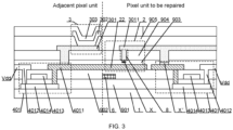
- FIGS. 2 and 3 illustrate an array substrate provided by some embodiments of the present disclosure.
- the array substrate provided by some embodiments of the present disclosure includes a base substrate 1 and a plurality of pixel units arranged in an array on the base substrate 1.
- Each pixel unit includes an open-circuit repair structure 2, an OLED 3, and a pixel driving circuit 4.
- the open-circuit repair structure 2 includes a repair line 22, and an orthographic projection of the repair line 22 in a pixel unit to be repaired on the base substrate 1 partially or completely overlaps with an orthographic projection of of an extension line (3011) of an anode 301 of the OLED on the base substrate 1 to form an overlapping region.
- the open-circuit repair point X is located in the overlapping region.
- the above array substrate is prone to a defect, i.e., the open-circuit point X', in the manufacturing process due to its complicated pixel driving structure.
- the repair line 22 has an overlapping portion with the anode 301 of the OLED, and the overlapping portion is embodied on an orthographic projection of the two on the substrate, so that the open-circuit repair point X is located in the overlapping region, enabling the anode 301 of the OLED of any one of two adjacent pixel units to be coupled to a drain 4011 of the driving thin film transistor 401 of another pixel unit of the two adjacent pixel units, thereby repairing the open-circuit point X' without affecting other components.
- the driving thin film transistor 401 in a case where an open circuit, i.e., an open-circuit point X', occurs between the drain 4011 of the driving thin film transistor 401 and the anode 301 of the OLED, the driving thin film transistor 401 cannot be coupled to the anode 301 of the OLED, so the pixel unit cannot emit light.
- the pixel unit is referred to as a pixel unit to be repaired, and a pixel unit around it is referred to as an adjacent pixel unit.
- the drain 4011 of the driving thin film transistor 401 in the adjacent pixel unit adjacent to the pixel unit to be repaired is coupled to the repair line 22, and the repair line 22 is coupled to the anode 301 of the OLED in the pixel unit to be repaired, the open-circuit point X' is repaired, so that the anode 31 of the OLED in the pixel unit to be repaired is coupled to the drain 4011 of the driving thin film transistor 401 in the adjacent pixel unit, thereby causing the pixel unit to be repaired to be restored to emit light.
- the plurality of pixel units are arranged in an array on the base substrate 1 of the array substrate.
- the pixel driving circuit 4 of one of the plurality of pixel units is open circuit, the pixel unit is defined as a pixel unit to be repaired, and a pixel unit around the pixel unit arranged on the base substrate 1 is defined as an adjacent pixel unit.
- the pixel unit to be repaired and the adjacent pixel unit belong to a same type of pixel units, and have a same structure and function.
- a division is only for the purpose of clearly explaining the specific structure of the array substrate, that is, defining a target pixel unit that may require an open-circuit repair as a pixel unit to be repaired, and another pixel unit adjacent to the pixel unit to be repaired is defined as an adjacent pixel unit.
- another pixel unit of the two adjacent pixel units is referred to as the adjacent pixel unit.
- the anode 301 of the OLED and the repair line 22 are located in a same pixel unit. Since the anode 301 of the OLED is provided in the pixel unit, the array substrate having the pixel unit shall be an OLED substrate, that is, each pixel unit of the array substrate is correspondingly provided with an OLED 3 and a pixel driving circuit 4 coupled to the anode 301 of the OLED.
- the OLED 3 may be any one of a top-emitting OLED, a bottom-emitting OLED, or a double-sided emitting OLED.
- FIG. 2 Only four pixel units arranged in an array are shown in FIG. 2 , which are used for emitting light of same or different colors. However, it will be understood by those skilled in the art that the number of pixel units included in the array substrate in the embodiments of the present disclosure is not limited to the four shown, and may include more, and colors of the light emitted by the pixel units are not limited.
- the pixel driving circuit 4 includes at least one thin film transistor.
- the at least one thin film transistor includes a driving thin film transistor 401 and a switching thin film transistor 402.
- the pixel driving circuit 4 for the OLED 3 includes at least one thin film transistor.
- the thin film transistor is a driving thin film transistor 401.
- the driving thin film transistor 401 refers to a thin film transistor in which the drain 4011 is coupled to the anode 301 of the OLED.
- the drain 4011 of the driving thin film transistor 401 and the anode 301 of the OLED may be electrically connected.
- the provided repair line 22 is coupled to the drain 4011 of the driving thin film transistor 401 in the adjacent pixel unit.
- An insulating film layer is disposed between the repair line 22 and the anode 301 of the OLED in the pixel unit to be repaired.
- An orthographic projection of the repair line 22 on the base substrate 1 has an overlapping region with an orthographic projection of the anode 301 of the OLED in the pixel unit to be repaired on the base substrate 1.
- the insulating film layer disposed between the repair line 22 and the anode 301 of the OLED may prevent the repair line 22 from contacting the anode 301 of the OLED, thereby preventing a short circuit between the drain 4011 and the anode 301.
- a film layer for insulation is provided between the anode 301 of the OLED in the pixel unit to be repaired and the repair line 22, and a portion of the anode 301 of the OLED in the pixel unit to be repaired corresponding to the overlapping region is disposed opposite to a portion of the repair line 22 corresponding to the overlapping region.
- the anode 301 of the OLED of the pixel unit to be repaired is coupled to the repair line 22 by deep penetration laser welding, so that the anode 301 of the OLED of the pixel unit to be repaired and the drain 4011 of the driving thin film transistor 401 in the adjacent pixel unit may be coupled by using the anode 301 of the OLED in the pixel unit to be repaired and the repair line 22.
- the pixel driving circuit 4 of the OLED 3 includes two thin film transistors, which are a switching thin film transistor 402 and a driving thin film transistor 401.
- a gate 4021 of the switching thin film transistor 402 is coupled to a gate line 6, and a source 4022 of the switching thin film transistor 402 is coupled to a data line 7, and a drain 4023 of the switching thin film transistor 402 is coupled to the gate 4013 of the driving thin film transistor 401 and the first plate C1 of the storage capacitor.
- a source 4012 of the driving thin film transistor 401 is coupled to the second plate C2 of the storage capacitor and the power line Vdd, and the drain 4011 of the driving thin film transistor 401 is coupled to the anode 301 of the OLED.
- the gate line 6 and the data line 7 may be made of one or more of the metal materials, such as copper (Cu), aluminum (Al), molybdenum (Mo), titanium (Ti), chromium (Cr), and tungsten (W), or their alloy materials.
- the metal materials such as copper (Cu), aluminum (Al), molybdenum (Mo), titanium (Ti), chromium (Cr), and tungsten (W), or their alloy materials.
- a single-layer metal wire is made of copper, and a laminated metal wire is made of Mo ⁇ Al ⁇ Mo, a laminated metal wire is made of Ti ⁇ Cu ⁇ Ti, or a laminated metal wire is made of MoTi ⁇ Cu, etc.
- the open-circuit repair structure 2 in the pixel unit to be repaired may be utilized to effectively repair the pixel unit to be repaired, and the anode 301 of the OLED in the pixel unit to be repaired may be coupled to the drain 4011 of the driving thin film transistor 401 in the adjacent pixel unit, so that the OLED 3 in the pixel unit to be repaired may be driven by the driving thin film transistor 401 in the adjacent pixel unit to ensure the normal use of the array substrate.
- the pixel units in the array substrate are generally arranged in an array on the base substrate 1. Pixel units in a same row are provided with a control signal by a same gate line 6, and pixel units in a same column are provided with a data signal by a same data line 7.
- the gate line 6 and the gates of the thin film transistors in the pixel units are generally disposed in a same layer, and the data line 7 and the sources and the drains of the thin film transistors in the pixel units are generally disposed in a same layer.
- the gate lines and the data lines are disposed crosswise to form a grid structure, so that a single pixel unit is correspondingly disposed in a single grid.
- Each pixel unit may be a pixel unit to be repaired, or an adjacent pixel unit around a pixel unit to be repaired.
- each pixel unit generally includes a driving thin film transistor 401 disposed on the base substrate 1, and an OLED 3 disposed at a side of the driving thin film transistor 401 away from the base substrate 1.
- the OLED 3 generally includes an OLED anode 301 and an OLED cathode 303 disposed opposite to each other, and an OLED light-emitting layer 302 disposed between the OLED anode 301 and the OLED cathode 303.
- the OLED cathode 303 is generally made of a metal material such as aluminum (Al)
- the OLED anode 301 is generally made of the indium tin oxide (ITO) material.
- the OLED light-emitting layer 302 may be a single-layer organic light-emitting layer, or a multilayer structure formed of a hole transport layer, an organic light-emitting layer, an electron transport layer, or the like.
- the driving thin film transistor 401 may be any one of an oxide semiconductor thin film transistor, a polysilicon thin film transistor, or an amorphous silicon thin film transistor according to the working principle of the thin film transistor.
- the driving thin film transistor 401 may be any one of a top-gate thin film transistor or a bottom-gate thin film transistor according to the position where the gate of the thin film transistor is disposed, which is not specifically limited in the embodiments of the present disclosure.
- the top-gate thin film transistor includes an active layer 4014, a gate insulating layer 901, a gate 4013, and an interlayer insulating layer 902 stacked on the base substrate 1.
- a drain 4011 and a source 4012 are disposed on the interlayer insulating layer 902.
- the drain 4011 and the source 4012 are coupled to the active layer 4014 respectively through via holes correspondingly formed in the interlayer insulating layer 902 and the gate insulating layer 901.
- the active layer 4014 may be an indium gallium zinc oxide (IGZO) layer.
- the gate insulating layer 901 may be a single layer structure such as a silicon nitride layer or a silicon oxide layer, or a multilayer structure such as a stacked structure formed of a silicon nitride layer and a silicon oxide layer.
- a passivation layer 903, a planarization layer 904, and a pixel defining layer 905 are generally disposed on a surface of the drain 4011 of the driving thin film transistor 401 away from the base substrate 1.
- the light-emitting layer 302 of the OLED 3 is disposed in an open region of the pixel defining layer 905.
- the passivation layer 903 may be a single layer structure, such as a silicon nitride layer or a silicon oxide layer, or may be a multilayer structure, such as a stacked structure formed of a silicon nitride layer and a silicon oxide layer.
- the planarization layer 904 is generally a resin layer having a thickness of 1 ⁇ m to 4 ⁇ m and made of an organic resin material.
- via holes are formed in the passivation layer 903 and the planarization layer 904.
- the anode 301 of the OLED is coupled to the drain 4011 of the driving thin film transistor 401 through the via hole formed in the planarization layer 904 and the passivation layer 903.
- the passivation layer 903 and the planarization layer 904 disposed between the repair line 22 and the anode 301 of the OLED of the pixel unit to be repaired.
- the adjacent pixel unit of the pixel unit to be repaired is a pixel unit in an adjacent row and a same column of the pixel unit to be repaired, that is, any one of the pixel units in adjacent rows and the same column of the pixel unit to be repaired.
- the repair line 22 may be provided as an extension line of the drain 4011 of the driving thin film transistor 401 of the pixel unit in the adjacent row and the same column.
- the repair line 22 and the drain 4011 of the driving thin film transistor 401 are integrally formed, which may not only simplify the manufacturing process of the pixel repair structure 2 in the pixel unit to be repaired to facilitate the fabrication of the array substrate, but also ensure that the repair line 22 is reliably coupled to the drain 4011 of the driving thin film transistor 401 of the pixel unit in the adjacent row and the same column.
- an orthographic projection of the extension line of the drain 4011 on the base substrate 1 partially or completely overlaps with an orthographic projection of an anode extension line 3011 of the anode 301 of the OLED in the pixel unit to be repaired on the base substrate to form an overlapping region.
- the anode extension line 3011 of the anode 301 of the OLED refers to a portion of the anode 301 of the OLED corresponding to the extension line of the drain 4011, that is, the anode extension line 3011 is an integral part of the anode 301 of the OLED.
- the space occupation of the open-circuit repair structure 2 may be optimized while the open-circuit repair structure 2 in the pixel unit to be repaired is formed, which is beneficial to improving the space utilization of the array substrate.
- a groove 8 is disposed in a region of the planarization layer 904 corresponding to the open-circuit repair point X.
- the groove depth of the groove 8 is less than or equal to the thickness of the planarization layer 904.
- the distance between the extension line 3011 and the repair line 22 in a corresponding region where the open-circuit repair point X is located is effectively shortened, so as to ensure the reliable welding between the anode extension line 3011 and the repair line 22 when the anode extension line 3011 and the repair line 22 are welded by means of the deep penetration laser welding, thereby improving the conduction reliability of the anode extension line 3011 and the repair line 22 after being repaired and coupled, that is, improving the repair reliability of the open-circuit repair structure 2.
- the gate line 6 and the gates of the thin film transistors in the pixel units are generally disposed in the same layer
- the data line 7 and the sources and the drains of the thin film transistors in the pixel units are generally disposed in the same layer
- the gate lines and the data lines are disposed crosswise.
- an orthogonal projection of the repair line 22 on the base substrate 1 intersects with an orthographic projection of a corresponding gate line 6 on the base substrate 1.
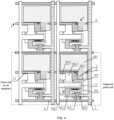
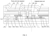
- FIGS. 4 and 5 provide another arrangement of the pixel units to be repaired and the adjacent pixel units on the array substrate.
- FIG. 4 is another schematic top view of an array substrate, in accordance with some embodiments of the present disclosure.
- the difference between the array substrate shown in FIGS. 4 and 5 and the array substrate shown in FIGS. 2 and 3 mainly lies in the arrangement of the repair line 22 in the open-circuit repair structure 2.
- other structures in the pixel unit such as the OLED or the driving thin film transistor, are the same as or similar to those in the array substrate shown in FIGS. 2 and 3 , which will not be described again.
- the relevant parts can refer to part of the description of the array substrate shown in FIGS. 2 and 3 .
- every two adjacent pixel units are pixel units in the adjacent columns and the same row, that is, the adjacent pixel unit of the pixel unit to be repaired is a pixel unit in the adjacent column and the same row of the pixel unit to be repaired.
- the repair line 22 in the open-circuit repair structure 2 of the pixel unit to be repaired is coupled to the drain 4011 of the driving thin film transistor 401 of the pixel unit in the adjacent column and the same row.
- the anode 301 of the OLED of the pixel unit to be repaired and the repair line 22 may be utilized to achieve that the anode 301 of the OLED in the pixel unit to be repaired and the drain 4011 of the driving thin film transistor of the pixel unit in the adjacent column and the same row are coupled, thereby driving the OLED 3 in the pixel unit to be reparied by utilizing the driving thin film transistor 401 of the pixel unit in the adjacent column and the same row.
- the drain 4011 of the driving thin film transistor 401 of the adjacent pixel unit is coupled to the repair line 22 in the pixel unit to be repaired, the drain 4011 of the driving thin film transistor 401 of the adjacent pixel unit is coupled to the anode 301 of the OLED in the pixel unit to be repaired through the repair line 22, thereby repairing the open circuit, and the pixel unit to be repaired re-emit light.
- the pixel units in the array substrate are generally arranged in an array on the base substrate. Pixel units in a same row are provided with a control signal by a same gate line 6, and pixel units in a same column are provided with a data signal by a same data line 7.
- the gate line 6 is generally disposed in the same layer as the gates of the thin film transistors in the pixel units
- the data line 7 is generally disposed in the same layer as the sources and the drains of the thin film transistors of the pixel units.
- Gate lines and data lines are disposed crosswise to form a grid structure, so that a single pixel unit is correspondingly disposed in a single grid.
- Each pixel unit may be a pixel unit to be repaired, or an adjacent pixel unit around a pixel unit to be repaired.
- FIG. 4 only four pixel units arranged in an array are shown in FIG. 4 , which are used for emitting light of the same or different colors.
- the number of pixel units provided by the array substrate provided by the embodiments of the present disclosure is not limited to the four shown, and may include more, and colors of the light emitted by the pixel units are not limited.
- the data line 7 and the sources and the drains of the thin film transistors in the pixel units are generally disposed in the same layer.
- the repair line 22 In a case where the repair line 22 is coupled to the drain 4011 of the driving thin film transistor 401 of the pixel unit in the adjacent column and the same row, the repair line 22 needs to correspondingly pass through a region where the data line 7 is disposed. Therefore, in order to prevent the repair line 22 from being coupled to the data line 7, in some embodiments of the present disclosure, the repair line 22 and the gate 4013 of the driving thin film transistor 401 of the pixel unit in the adjacent column and the same row are disposed in the same layer and insulated from each other.
- the gate 4013 of the driving thin film transistor 401 of each pixel unit is disposed at a side of the drain 4011 away from the anode 301 of the OLED, and an interlayer insulating layer 902 is provided between the gate 4013 and the drain 4011.
- the repair line 22 in the pixel unit to be repaired and the gate 4013 of the driving thin film transistor 401 in the pixel unit to be repaired are disposed in the same layer and insulated from each other.
- the repair line 22 and the gate 4013 of the driving thin film transistor 401 may be formed in a single patterning process, which is advantageous for simplifying the manufacturing process of the open-circuit repair structure in the pixel unit to improve the production efficiency of the array substrate.
- via holes are formed in the interlayer insulating layer 902.
- the drain 4011 of the driving thin film transistor 401 of the pixel unit in the adjacent column and the same row is coupled to the repair line 22 through the via hole provided in the interlayer insulating layer 902.
- an orthographic projection of the repair line 22 on the base substrate intersects with an orthographic projection of a corresponding data line 7 on the base substrate.
- the passivation layer 903 and the planarization layer 904 are generally stacked on a surface of the drain 4011 of the driving thin film transistor 401 proximate to the anode 301 of the OLED.
- the anode 301 of the OLED is coupled to the drain 4011 of the driving thin film transistor 401 through the via hole provided in the planarization layer 904 and the passivation layer 903.
- the interlayer insulating layer 902, the passivation layer 903, and the planarization layer 904 are sequentially disposed between the repair line 22 and the anode 301 of the OLED in the pixel unit to be repaired.
- a groove 8 is formed in a region of the planarization layer 904 corresponding to the open-circuit repair point X, and a groove 8 may also be formed in regions of the planarization layer 904 and the passivation layer 903 corresponding to the open-circuit repair point X.
- the groove depth of the groove 8 is less than or equal to the total thickness of the planarization layer 904 and the passivation layer 903.
- the anode 301 of the OLED in the pixel unit to be repaired is formed by deposition
- the anode 301 of the OLED covers and fills the groove 8, and in this way, the distance between the anode 301 of the OLED in the pixel unit to be repaired and the repair line 22 in a corresponding region of the open-circuit repair point X is effectively shortened, so as to ensure the reliable welding between the anode 301 of the OLED in the pixel unit to be repaired and the repair line 22 when the anode 301 and the repair line 22 are welded by means of the deep penetration laser welding, thereby improving the conduction reliability of the anode 301 of the OLED in the pixel unit to be repaired and the repair line 22 after being repaired and coupled, that is, improving the repair reliability of the open-circuit repair structure 2.
- the pixel defining layer 905 is generally disposed on a surface of the planarization layer 904 away from the base substrate 1.
- the pixel defining layer 905 is generally a resin layer having a thickness of 1 ⁇ m to 3 ⁇ m and made of an organic resin material.
- the light-emitting layer 302 of the OLED 3 is generally disposed in an open region of the pixel defining layer 905.
- a portion of the anode 301 of the OLED corresponding to the open-circuit repair point X is covered with the pixel defining layer 905, so that the open-circuit repair structure of a normal array substrate is insulated and protected by utilizing the pixel defining layer 905.
- the display device includes the above array substrate.
- the array substrate includes a base substrate and a plurality of pixel units arranged in an array on the base substrate.
- Each pixel unit includes an open-circuit repair structure, an OLED, and a pixel driving circuit, and the open-circuit repair structure includes a repair line.
- An orthographic projection of the repair line in the pixel unit to be repaired on the base substrate partially or completely overlaps with an orthographic projection of the anode of the OLED in the pixel unit to be repaired on the base substrate to form an overlapping region.
- An open-circuit repair point is disposed in the overlapping region.
- the array substrate in the display device has same advantages as the array substrate in the above embodiments, which will not be described herein again.
- the display device may be a product or component having a display function, such as a mobile phone, a tablet computer, a television, a display, a notebook computer, a digital photo frame, or a navigator.
- a display function such as a mobile phone, a tablet computer, a television, a display, a notebook computer, a digital photo frame, or a navigator.
Landscapes
- Engineering & Computer Science (AREA)
- Microelectronics & Electronic Packaging (AREA)
- Manufacturing & Machinery (AREA)
- Physics & Mathematics (AREA)
- Optics & Photonics (AREA)
- Geometry (AREA)
- Electroluminescent Light Sources (AREA)
- Devices For Indicating Variable Information By Combining Individual Elements (AREA)
Claims (13)
- Arraysubstrat, umfassend:ein Basissubstrat (1);eine Vielzahl von Pixeleinheiten, die in einem Array auf einem Basissubstrat (1) angeordnet sind, wobei jede Pixeleinheit eine Leerlaufreparaturstruktur (2), eine organische Leuchtdiode (OLED) (3) und eine Pixeltreiberschaltung (4) einschließt, wobei die Leerlaufreparaturstruktur (2) eine Reparaturleitung (22) einschließt; undeine isolierende Zwischenschicht (902), eine Passivierungsschicht (903) und eine Planarisierungsschicht (904), die nacheinander zwischen einer Anode (301) der OLED (3) in einer zu reparierenden Pixeleinheit der Vielzahl von Pixeleinheiten und der Reparaturleitung (22) in einer benachbarten Pixeleinheit neben der zu reparierenden Pixeleinheit gestapelt sind, wobeidie Pixeltreiberschaltung (4) in jeder Pixeleinheit einen treibenden Dünnschichttransistor (401) einschließt;eine orthogonale Projektion der Reparaturleitung (22) in der zu reparierenden Pixeleinheit auf dem Basissubstrat (1) sich teilweise mit einer orthogonalen Projektion der Anode (301) der OLED (3) in der zu reparierenden Pixeleinheit auf dem Basissubstrat (1) überlappt, und die Reparaturleitung (22) in der benachbarten Pixeleinheit mit einem Drain (4011) des treibenden Dünnschichttransistors (401) in der benachbarten Pixeleinheit gekoppelt ist;die zu reparierende Pixeleinheit und die benachbarte Pixeleinheit Pixeleinheiten in benachbarten Spalten und einer gleichen Zeile sind, die Reparaturleitung (22) in der zu reparierenden Pixeleinheit und ein Gate (4013) des treibenden Dünnschichttransistors (401) in der zu reparierenden Pixeleinheit elektrisch isoliert sind und in einer gleichen Schicht angeordnet sind, und die isolierende Zwischenschicht (902) zwischen der Reparaturleitung (22) in der zu reparierenden Pixeleinheit und dem Drain (4011) des treibenden Dünnschichttransistors in der zu reparierenden Pixeleinheit angeordnet ist;dadurch gekennzeichnet, dass:eine Rille (8) in der Planarisierungsschicht (904) gebildet ist, und
sich in einem Bereich befindet, in dem sich die orthogonale Projektion der Reparaturleitung (22) in der zu reparierenden Pixeleinheit auf dem Basissubstrat (1) teilweise mit der orthogonalen Projektion der Anode (301) der OLED (3) in der zu reparierenden Pixeleinheit auf dem Basissubstrat (1) überlappt, und ein Abschnitt der Anode (301) der OLED (3) in der zu reparierenden Pixeleinheit in die Rille (8) gefüllt ist; undeine Rillentiefe der Rille (8) kleiner oder gleich einer Gesamtdicke der Passivierungsschicht (903) und der Planarisierungsschicht (904) ist, sodass die Reparaturleitung (22) in der zu reparierenden Pixeleinheit und die Anode (301) der OLED (3) in der zu reparierenden Pixeleinheit nicht durch die Rille (8) gekoppelt sind, bevor die zu reparierende Pixeleinheit repariert wird. - Arraysubstrat nach Anspruch 1, wobei die Pixeltreiberschaltung (4) weiter einen schaltenden Dünnschichttransistor (402) einschließt.
- Arraysubstrat nach Anspruch 1, wobei Durchgangslöcher in der isolierenden Zwischenschicht (902) ausgebildet sind und der Drain (4011) des treibenden Dünnschichttransistors (401) in der benachbarten Pixeleinheit mit der Reparaturleitung (22) in der benachbarten Pixeleinheit durch ein entsprechendes der Durchgangslöcher gekoppelt ist.
- Arraysubstrat nach Anspruch 2, weiter umfassend Gateleitungen (6) und Datenleitungen (7), die kreuzweise angeordnet sind, wobei ein Gate (4021) des schaltenden Dünnschichttransistors (402) mit einer entsprechenden Gateleitung (6) gekoppelt ist und ein Source (4022) des schaltenden Dünnschichttransistors (402) mit einer entsprechenden Datenleitung (7) gekoppelt ist.
- Arraysubstrat nach Anspruch 1, weiter umfassend Gateleitungen (6) und Datenleitungen (7), die kreuzweise angeordnet sind,wobei Pixeleinheiten in einer gleichen Spalte einer gleichen Datenleitung (7) entsprechen; undeine orthogonale Projektion der Reparaturleitung (22) in jeder Pixeleinheit auf dem Basissubstrat (1) sich mit einer orthogonalen Projektion einer entsprechenden Datenleitung (7) auf dem Basissubstrat (1) schneidet.
- Arraysubstrat nach Anspruch 1, weiter umfassend eine pixeldefinierende Schicht (905), die auf Oberflächen von Anoden (301) von OLEDs (3) angeordnet ist, die vom Basissubstrat (1) abgewandt sind.
- Anzeigevorrichtung, die ein Arraysubstrat nach Anspruch 1 umfasst.
- Arraysubstrat, umfassend:ein Basissubstrat (1); undeine Vielzahl von Pixeleinheiten, die in einem Array auf einem Basissubstrat (1) angeordnet sind, wobei jede Pixeleinheit eine Leerlaufreparaturstruktur (2), eine organische Leuchtdiode (OLED) und eine Pixeltreiberschaltung (4) einschließt, wobei die Leerlaufreparaturstruktur (2) eine Reparaturleitung (22) einschließt, wobeidie Pixeltreiberschaltung (4) einen treibenden Dünnschichttransistor (401) einschließt;eine orthogonale Projektion der Reparaturleitung (22) in einer zu reparierenden Pixeleinheit der Vielzahl von Pixeleinheiten auf dem Basissubstrat (1) sich teilweise mit einer orthogonalen Projektion einer Erstreckungsleitung (3011) einer Anode (301) der OLED in der zu reparierenden Pixeleinheit auf dem Basissubstrat (1) überlappt, und die Reparaturleitung (22) in der benachbarten Pixeleinheit mit einem Drain (4011) des treibenden Dünnschichttransistors (401) in der benachbarten Pixeleinheit gekoppelt ist;die zu reparierende Pixeleinheit und die benachbarte Pixeleinheit Pixeleinheiten in benachbarten Zeilen und einer gleichen Spalte sind, die Reparaturleitung (22) in der benachbarten Pixeleinheit eine Erstreckungsleitung des Drains (4011) des treibenden Dünnschichttransistors (401) in der benachbarten Pixeleinheit ist;eine orthogonale Projektion einer Erstreckungsleitung der Anode (3011) der OLED in der zu reparierenden Pixeleinheit auf dem Basissubstrat (1) sich teilweise mit einer orthogonalen Projektion der Erstreckungsleitung des Drains (4011) des treibenden Dünnschichttransistors (401) in der benachbarten Pixeleinheit auf dem Basissubstrat (1) überlappt;das Arraysubstrat weiter eine Passivierungsschicht (903) und eine Planarisierungsschicht (904) umfasst, die zwischen der Erstreckungsleitung des Drains (4011) des treibenden Dünnschichttransistors (401) in der benachbarten Pixeleinheit und der Erstreckungsleitung der Anode (3011) der OLED in der zu reparierenden Pixeleinheit gestapelt sind;dadurch gekennzeichnet, dass:eine Rille (8) in der Planarisierungsschicht (904) ausgebildet ist und sich in einem Bereich befindet, in dem sich eine orthogonale Projektion der Erstreckungsleitung des Drains (4011) des treibenden Dünnschichttransistors (401) in der benachbarten Pixeleinheit auf dem Basissubstrat (1) teilweise mit einer orthogonalen Projektion der Erstreckungsleitung (3011) der Anode der OLED in der zu reparierenden Pixeleinheit auf dem Basissubstrat (1) überlappt, und
ein Abschnitt der Erstreckungsleitung der Anode (301) der OLED in der zu reparierenden Pixeleinheit in die Rille (8) gefüllt wird; undeine Rillentiefe der Rille (8) kleiner oder gleich einer Gesamtdicke der Planarisierungsschicht (904) ist, sodass die Erstreckungsleitung des Drains (4011) des treibenden Dünnschichttransistors (401) in der benachbarten Pixeleinheit und die Erstreckungsleitung der Anode (301) der OLED in der zu reparierenden Pixeleinheit nicht durch die Rille (8) gekoppelt sind, bevor die zu reparierende Pixeleinheit repariert wird. - Arraysubstrat nach Anspruch 8, wobei die Pixeltreiberschaltung (4) weiter einen schaltenden Dünnschichttransistor (402) einschließt.
- Arraysubstrat nach Anspruch 9, weiter umfassend Gateleitungen (6) und Datenleitungen (7), die kreuzweise angeordnet sind, wobei ein Gate (4021) des schaltenden Dünnschichttransistors (402) mit einer entsprechenden Gateleitung (6) gekoppelt ist und ein Source (4022) des schaltenden Dünnschichttransistors (402) mit einer entsprechenden Datenleitung (7) gekoppelt ist.
- Arraysubstrat nach Anspruch 8, weiter umfassend Gateleitungen (6) und Datenleitungen (7), die kreuzweise angeordnet sind, wobei Pixeleinheiten in einer gleichen Zeile einer gleichen Gateleitung (6) entsprechen; und
eine orthogonale Projektion der Reparaturleitung (22) in jeder Pixeleinheit auf dem Basissubstrat (1) sich mit einer orthogonalen Projektion einer entsprechenden Gateleitung (6) auf dem Basissubstrat (1) schneidet. - Arraysubstrat nach Anspruch 8, weiter umfassend eine pixeldefinierende Schicht (905), die auf Oberflächen von Anoden (301) von OLEDs (3) angeordnet ist, die vom Basissubstrat (1) abgewandt sind.
- Anzeigevorrichtung, die ein Arraysubstrat nach Anspruch 8 umfasst.
Applications Claiming Priority (2)
| Application Number | Priority Date | Filing Date | Title |
|---|---|---|---|
| CN201721127658.4U CN207134356U (zh) | 2017-09-04 | 2017-09-04 | 一种阵列基板及显示装置 |
| PCT/CN2018/103994 WO2019042474A1 (zh) | 2017-09-04 | 2018-09-04 | 阵列基板及显示装置 |
Publications (3)
| Publication Number | Publication Date |
|---|---|
| EP3680935A1 EP3680935A1 (de) | 2020-07-15 |
| EP3680935A4 EP3680935A4 (de) | 2021-05-05 |
| EP3680935B1 true EP3680935B1 (de) | 2025-02-12 |
Family
ID=61637771
Family Applications (1)
| Application Number | Title | Priority Date | Filing Date |
|---|---|---|---|
| EP18849825.7A Active EP3680935B1 (de) | 2017-09-04 | 2018-09-04 | Arraysubstrat und anzeigevorrichtung |
Country Status (6)
| Country | Link |
|---|---|
| US (1) | US10991917B2 (de) |
| EP (1) | EP3680935B1 (de) |
| JP (1) | JP7212617B2 (de) |
| KR (1) | KR102277886B1 (de) |
| CN (1) | CN207134356U (de) |
| WO (1) | WO2019042474A1 (de) |
Families Citing this family (25)
| Publication number | Priority date | Publication date | Assignee | Title |
|---|---|---|---|---|
| CN207134356U (zh) | 2017-09-04 | 2018-03-23 | 京东方科技集团股份有限公司 | 一种阵列基板及显示装置 |
| CN110165058A (zh) * | 2018-03-26 | 2019-08-23 | 京东方科技集团股份有限公司 | 阵列基板及其制备方法、修复方法、显示装置 |
| CN110061035A (zh) * | 2019-04-24 | 2019-07-26 | 合肥京东方卓印科技有限公司 | 阵列基板及显示装置 |
| CN210073855U (zh) * | 2019-08-26 | 2020-02-14 | 北京京东方技术开发有限公司 | 阵列基板、显示面板和显示装置 |
| CN110568678B (zh) | 2019-09-26 | 2021-01-01 | 深圳市华星光电技术有限公司 | 显示面板 |
| CN110764289B (zh) * | 2019-10-29 | 2022-03-29 | Tcl华星光电技术有限公司 | 液晶面板修补方法 |
| CN110797351B (zh) * | 2019-11-08 | 2022-05-20 | 京东方科技集团股份有限公司 | 一种阵列基板、其检测方法、显示面板及显示装置 |
| KR102184724B1 (ko) | 2019-12-31 | 2020-12-01 | 엘지디스플레이 주식회사 | 표시 장치 및 그의 제조 방법 |
| CN112216706B (zh) * | 2020-11-13 | 2022-07-29 | 武汉华星光电技术有限公司 | 驱动背板及发光基板 |
| KR20220086963A (ko) * | 2020-12-17 | 2022-06-24 | 엘지디스플레이 주식회사 | 투명 표시 장치 |
| KR20220090275A (ko) * | 2020-12-22 | 2022-06-29 | 엘지디스플레이 주식회사 | 투명 표시 장치 |
| KR102907184B1 (ko) * | 2020-12-30 | 2025-12-31 | 엘지디스플레이 주식회사 | 발광표시패널 및 이를 이용한 발광표시장치 |
| CN115568245B (zh) * | 2021-01-29 | 2026-02-06 | 湖北长江新型显示产业创新中心有限公司 | 一种显示面板和显示装置 |
| CN112992932A (zh) | 2021-02-05 | 2021-06-18 | 深圳市华星光电半导体显示技术有限公司 | 阵列基板及其制备方法、短路修补方法 |
| CN113257883B (zh) | 2021-07-07 | 2021-09-24 | 北京京东方技术开发有限公司 | 显示基板及其制备方法、显示装置 |
| KR102921910B1 (ko) | 2021-07-12 | 2026-02-03 | 삼성디스플레이 주식회사 | 표시 장치 |
| CN114023761A (zh) * | 2021-09-28 | 2022-02-08 | 惠科股份有限公司 | 阵列基板、显示面板及其坏点修复方法 |
| KR20230096533A (ko) * | 2021-12-23 | 2023-06-30 | 엘지디스플레이 주식회사 | 리페어 구조를 갖는 전계 발광 표시장치 |
| KR20230099293A (ko) * | 2021-12-27 | 2023-07-04 | 엘지디스플레이 주식회사 | 리페어 구조를 갖는 전계 발광 표시장치 |
| CN114420882B (zh) * | 2022-01-12 | 2023-09-05 | 深圳市华星光电半导体显示技术有限公司 | 显示面板及其修复方法、显示装置 |
| CN114613816B (zh) | 2022-03-02 | 2025-07-08 | 深圳市华星光电半导体显示技术有限公司 | 显示面板及其修复方法、显示装置 |
| CN115568249A (zh) * | 2022-10-25 | 2023-01-03 | 合肥鑫晟光电科技有限公司 | 显示基板及制备方法、显示面板及修复方法、显示装置 |
| KR20240093193A (ko) * | 2022-12-15 | 2024-06-24 | 엘지디스플레이 주식회사 | 발광 표시 장치 |
| CN117975882A (zh) * | 2023-12-29 | 2024-05-03 | 湖北长江新型显示产业创新中心有限公司 | 显示面板及其像素修复方法、显示装置 |
| KR20250112987A (ko) * | 2024-01-18 | 2025-07-25 | 엘지디스플레이 주식회사 | 표시 장치 및 표시 패널 |
Family Cites Families (18)
| Publication number | Priority date | Publication date | Assignee | Title |
|---|---|---|---|---|
| JP2003050400A (ja) | 2001-08-08 | 2003-02-21 | Toshiba Corp | アクティブマトリクス型液晶表示装置及びその製造方法 |
| KR101022156B1 (ko) * | 2009-02-16 | 2011-03-17 | 삼성모바일디스플레이주식회사 | 유기전계발광 표시장치의 화소수리구조 및 그 수리방법 |
| KR101910113B1 (ko) * | 2012-03-16 | 2018-10-22 | 삼성디스플레이 주식회사 | 유기 발광 표시 장치 및 그 제조 방법 |
| KR101993334B1 (ko) | 2013-04-01 | 2019-06-27 | 삼성디스플레이 주식회사 | 유기 발광 표시 장치, 유기 발광 표시 장치의 리페어 방법 및 유기 발광 표시 장치의 구동 방법 |
| CN103345093B (zh) * | 2013-06-28 | 2015-12-02 | 京东方科技集团股份有限公司 | 像素单元、阵列基板及其制造、修复方法和显示装置 |
| TWI713943B (zh) | 2013-09-12 | 2020-12-21 | 日商新力股份有限公司 | 顯示裝置及電子機器 |
| KR102112649B1 (ko) | 2013-11-25 | 2020-05-19 | 엘지디스플레이 주식회사 | 유기전계 발광소자 및 이의 리페어 방법 |
| KR102123979B1 (ko) | 2013-12-09 | 2020-06-17 | 엘지디스플레이 주식회사 | 리페어 구조를 갖는 유기발광표시장치 |
| KR20150113530A (ko) * | 2014-03-31 | 2015-10-08 | 엘지디스플레이 주식회사 | 유기 발광 표시 장치 |
| KR102148487B1 (ko) * | 2014-05-08 | 2020-08-26 | 엘지디스플레이 주식회사 | 유기 전계 발광 표시 장치 및 그의 리페어 방법 |
| KR102145850B1 (ko) | 2014-05-30 | 2020-08-20 | 엘지디스플레이 주식회사 | 유기발광 디스플레이 장치와 픽셀의 리페어 방법 |
| KR20150142821A (ko) | 2014-06-11 | 2015-12-23 | 삼성디스플레이 주식회사 | 유기 발광 표시 장치 및 이의 리페어 방법 |
| KR102374833B1 (ko) * | 2014-11-25 | 2022-03-15 | 엘지디스플레이 주식회사 | 유기 발광 표시 장치 및 그 제조 방법 |
| KR102387784B1 (ko) * | 2014-12-29 | 2022-04-15 | 엘지디스플레이 주식회사 | 유기발광표시장치 및 이의 리페어 방법 |
| KR102333563B1 (ko) * | 2014-12-31 | 2021-12-01 | 엘지디스플레이 주식회사 | 유기발광 디스플레이 장치와 픽셀의 리페어 방법 |
| CN105161517B (zh) | 2015-08-14 | 2018-10-12 | 京东方科技集团股份有限公司 | 阵列基板的修复方法、修复装置和制备方法 |
| KR101795579B1 (ko) * | 2015-11-10 | 2017-11-08 | 엘지디스플레이 주식회사 | 유기 발광 표시 장치 및 그 제조 방법 |
| CN207134356U (zh) | 2017-09-04 | 2018-03-23 | 京东方科技集团股份有限公司 | 一种阵列基板及显示装置 |
-
2017
- 2017-09-04 CN CN201721127658.4U patent/CN207134356U/zh active Active
-
2018
- 2018-09-04 US US16/489,165 patent/US10991917B2/en active Active
- 2018-09-04 WO PCT/CN2018/103994 patent/WO2019042474A1/zh not_active Ceased
- 2018-09-04 JP JP2019527804A patent/JP7212617B2/ja active Active
- 2018-09-04 KR KR1020197031467A patent/KR102277886B1/ko active Active
- 2018-09-04 EP EP18849825.7A patent/EP3680935B1/de active Active
Also Published As
| Publication number | Publication date |
|---|---|
| KR20190129998A (ko) | 2019-11-20 |
| US20200013992A1 (en) | 2020-01-09 |
| EP3680935A4 (de) | 2021-05-05 |
| EP3680935A1 (de) | 2020-07-15 |
| JP2020532754A (ja) | 2020-11-12 |
| US10991917B2 (en) | 2021-04-27 |
| WO2019042474A1 (zh) | 2019-03-07 |
| KR102277886B1 (ko) | 2021-07-16 |
| CN207134356U (zh) | 2018-03-23 |
| JP7212617B2 (ja) | 2023-01-25 |
Similar Documents
| Publication | Publication Date | Title |
|---|---|---|
| EP3680935B1 (de) | Arraysubstrat und anzeigevorrichtung | |
| US10937849B2 (en) | Array substrate and method of manufacturing the same, display panel and display device | |
| US10971574B2 (en) | Display device | |
| KR102541447B1 (ko) | 유기 발광 표시 장치 | |
| KR102424597B1 (ko) | 플렉서블 유기발광다이오드 표시장치 및 그 제조 방법 | |
| US9064833B2 (en) | Organic light emitting diode display | |
| EP3200232B1 (de) | Organisches leuchtdioden-arraysubstrat und herstellungsverfahren dafür | |
| US7982386B2 (en) | Organic light emitting display device with opaque electrodes | |
| US20120050235A1 (en) | Organic electroluminescence emitting display and method of manufacturing the same | |
| JP2020505715A (ja) | 有機発光ダイオード(oled)アレイ基板及びその製造方法、表示装置 | |
| CN112133726A (zh) | 电致发光显示装置 | |
| JP2005331919A (ja) | 平板ディスプレイ装置及び電界発光ディスプレイ装置 | |
| KR20190066648A (ko) | 표시 장치 및 그 제조 방법 | |
| KR20210086247A (ko) | 표시 장치 | |
| US9806136B2 (en) | Organic light emitting diode display device and method for repairing organic light emitting diode display | |
| CN102576722A (zh) | El显示面板、el显示装置以及el显示面板的制造方法 | |
| US8841832B2 (en) | Organic light emitting diode display having improved strength by preventing the exfoliation of a sealant | |
| KR100879294B1 (ko) | 유기 발광 표시 장치 | |
| KR101796934B1 (ko) | 반사 전극을 구비한 유기전계발광 표시장치 및 그 제조 방법 | |
| US8368056B2 (en) | Organic light emitting diode display and method for manufacturing the same | |
| JP2001100655A (ja) | El表示装置 | |
| US10388910B2 (en) | Display device including a barrier layer and method for manufacturing the same | |
| WO2021027160A1 (zh) | 显示面板及其制作方法 | |
| KR102723489B1 (ko) | 유기 발광 표시 장치 | |
| US20240188341A1 (en) | Display device |
Legal Events
| Date | Code | Title | Description |
|---|---|---|---|
| STAA | Information on the status of an ep patent application or granted ep patent |
Free format text: STATUS: THE INTERNATIONAL PUBLICATION HAS BEEN MADE |
|
| PUAI | Public reference made under article 153(3) epc to a published international application that has entered the european phase |
Free format text: ORIGINAL CODE: 0009012 |
|
| STAA | Information on the status of an ep patent application or granted ep patent |
Free format text: STATUS: REQUEST FOR EXAMINATION WAS MADE |
|
| 17P | Request for examination filed |
Effective date: 20190925 |
|
| AK | Designated contracting states |
Kind code of ref document: A1 Designated state(s): AL AT BE BG CH CY CZ DE DK EE ES FI FR GB GR HR HU IE IS IT LI LT LU LV MC MK MT NL NO PL PT RO RS SE SI SK SM TR |
|
| AX | Request for extension of the european patent |
Extension state: BA ME |
|
| DAV | Request for validation of the european patent (deleted) | ||
| DAX | Request for extension of the european patent (deleted) | ||
| A4 | Supplementary search report drawn up and despatched |
Effective date: 20210401 |
|
| RIC1 | Information provided on ipc code assigned before grant |
Ipc: H01L 27/32 20060101ALI20210326BHEP Ipc: H01L 27/12 20060101AFI20210326BHEP |
|
| STAA | Information on the status of an ep patent application or granted ep patent |
Free format text: STATUS: EXAMINATION IS IN PROGRESS |
|
| 17Q | First examination report despatched |
Effective date: 20230605 |
|
| P01 | Opt-out of the competence of the unified patent court (upc) registered |
Effective date: 20230630 |
|
| REG | Reference to a national code |
Ref legal event code: R079 Ref country code: DE Ref legal event code: R079 Ref document number: 602018079149 Country of ref document: DE Free format text: PREVIOUS MAIN CLASS: H01L0027120000 Ipc: H10K0059131000 |
|
| GRAP | Despatch of communication of intention to grant a patent |
Free format text: ORIGINAL CODE: EPIDOSNIGR1 |
|
| STAA | Information on the status of an ep patent application or granted ep patent |
Free format text: STATUS: GRANT OF PATENT IS INTENDED |
|
| RIC1 | Information provided on ipc code assigned before grant |
Ipc: H01L 27/12 20060101ALN20240927BHEP Ipc: H10K 59/121 20230101ALN20240927BHEP Ipc: H10K 50/813 20230101ALN20240927BHEP Ipc: H10K 59/131 20230101AFI20240927BHEP |
|
| INTG | Intention to grant announced |
Effective date: 20241010 |
|
| GRAS | Grant fee paid |
Free format text: ORIGINAL CODE: EPIDOSNIGR3 |
|
| GRAA | (expected) grant |
Free format text: ORIGINAL CODE: 0009210 |
|
| STAA | Information on the status of an ep patent application or granted ep patent |
Free format text: STATUS: THE PATENT HAS BEEN GRANTED |
|
| AK | Designated contracting states |
Kind code of ref document: B1 Designated state(s): AL AT BE BG CH CY CZ DE DK EE ES FI FR GB GR HR HU IE IS IT LI LT LU LV MC MK MT NL NO PL PT RO RS SE SI SK SM TR |
|
| REG | Reference to a national code |
Ref country code: GB Ref legal event code: FG4D |
|
| REG | Reference to a national code |
Ref country code: CH Ref legal event code: EP |
|
| REG | Reference to a national code |
Ref country code: DE Ref legal event code: R096 Ref document number: 602018079149 Country of ref document: DE |
|
| REG | Reference to a national code |
Ref country code: IE Ref legal event code: FG4D |
|
| REG | Reference to a national code |
Ref country code: NL Ref legal event code: MP Effective date: 20250212 |
|
| PG25 | Lapsed in a contracting state [announced via postgrant information from national office to epo] |
Ref country code: RS Free format text: LAPSE BECAUSE OF FAILURE TO SUBMIT A TRANSLATION OF THE DESCRIPTION OR TO PAY THE FEE WITHIN THE PRESCRIBED TIME-LIMIT Effective date: 20250512 |
|
| PG25 | Lapsed in a contracting state [announced via postgrant information from national office to epo] |
Ref country code: FI Free format text: LAPSE BECAUSE OF FAILURE TO SUBMIT A TRANSLATION OF THE DESCRIPTION OR TO PAY THE FEE WITHIN THE PRESCRIBED TIME-LIMIT Effective date: 20250212 |
|
| PG25 | Lapsed in a contracting state [announced via postgrant information from national office to epo] |
Ref country code: PL Free format text: LAPSE BECAUSE OF FAILURE TO SUBMIT A TRANSLATION OF THE DESCRIPTION OR TO PAY THE FEE WITHIN THE PRESCRIBED TIME-LIMIT Effective date: 20250212 |
|
| PG25 | Lapsed in a contracting state [announced via postgrant information from national office to epo] |
Ref country code: ES Free format text: LAPSE BECAUSE OF FAILURE TO SUBMIT A TRANSLATION OF THE DESCRIPTION OR TO PAY THE FEE WITHIN THE PRESCRIBED TIME-LIMIT Effective date: 20250212 |
|
| REG | Reference to a national code |
Ref country code: LT Ref legal event code: MG9D |
|
| PG25 | Lapsed in a contracting state [announced via postgrant information from national office to epo] |
Ref country code: IS Free format text: LAPSE BECAUSE OF FAILURE TO SUBMIT A TRANSLATION OF THE DESCRIPTION OR TO PAY THE FEE WITHIN THE PRESCRIBED TIME-LIMIT Effective date: 20250612 Ref country code: NO Free format text: LAPSE BECAUSE OF FAILURE TO SUBMIT A TRANSLATION OF THE DESCRIPTION OR TO PAY THE FEE WITHIN THE PRESCRIBED TIME-LIMIT Effective date: 20250512 |
|
| PG25 | Lapsed in a contracting state [announced via postgrant information from national office to epo] |
Ref country code: NL Free format text: LAPSE BECAUSE OF FAILURE TO SUBMIT A TRANSLATION OF THE DESCRIPTION OR TO PAY THE FEE WITHIN THE PRESCRIBED TIME-LIMIT Effective date: 20250212 |
|
| PG25 | Lapsed in a contracting state [announced via postgrant information from national office to epo] |
Ref country code: HR Free format text: LAPSE BECAUSE OF FAILURE TO SUBMIT A TRANSLATION OF THE DESCRIPTION OR TO PAY THE FEE WITHIN THE PRESCRIBED TIME-LIMIT Effective date: 20250212 |
|
| PG25 | Lapsed in a contracting state [announced via postgrant information from national office to epo] |
Ref country code: PT Free format text: LAPSE BECAUSE OF FAILURE TO SUBMIT A TRANSLATION OF THE DESCRIPTION OR TO PAY THE FEE WITHIN THE PRESCRIBED TIME-LIMIT Effective date: 20250612 Ref country code: LV Free format text: LAPSE BECAUSE OF FAILURE TO SUBMIT A TRANSLATION OF THE DESCRIPTION OR TO PAY THE FEE WITHIN THE PRESCRIBED TIME-LIMIT Effective date: 20250212 |
|
| PG25 | Lapsed in a contracting state [announced via postgrant information from national office to epo] |
Ref country code: GR Free format text: LAPSE BECAUSE OF FAILURE TO SUBMIT A TRANSLATION OF THE DESCRIPTION OR TO PAY THE FEE WITHIN THE PRESCRIBED TIME-LIMIT Effective date: 20250513 Ref country code: BG Free format text: LAPSE BECAUSE OF FAILURE TO SUBMIT A TRANSLATION OF THE DESCRIPTION OR TO PAY THE FEE WITHIN THE PRESCRIBED TIME-LIMIT Effective date: 20250212 |
|
| REG | Reference to a national code |
Ref country code: AT Ref legal event code: MK05 Ref document number: 1767351 Country of ref document: AT Kind code of ref document: T Effective date: 20250212 |
|
| PG25 | Lapsed in a contracting state [announced via postgrant information from national office to epo] |
Ref country code: SE Free format text: LAPSE BECAUSE OF FAILURE TO SUBMIT A TRANSLATION OF THE DESCRIPTION OR TO PAY THE FEE WITHIN THE PRESCRIBED TIME-LIMIT Effective date: 20250212 |
|
| PG25 | Lapsed in a contracting state [announced via postgrant information from national office to epo] |
Ref country code: SM Free format text: LAPSE BECAUSE OF FAILURE TO SUBMIT A TRANSLATION OF THE DESCRIPTION OR TO PAY THE FEE WITHIN THE PRESCRIBED TIME-LIMIT Effective date: 20250212 |
|
| PG25 | Lapsed in a contracting state [announced via postgrant information from national office to epo] |
Ref country code: DK Free format text: LAPSE BECAUSE OF FAILURE TO SUBMIT A TRANSLATION OF THE DESCRIPTION OR TO PAY THE FEE WITHIN THE PRESCRIBED TIME-LIMIT Effective date: 20250212 |
|
| PGFP | Annual fee paid to national office [announced via postgrant information from national office to epo] |
Ref country code: DE Payment date: 20250919 Year of fee payment: 8 |
|
| PG25 | Lapsed in a contracting state [announced via postgrant information from national office to epo] |
Ref country code: IT Free format text: LAPSE BECAUSE OF FAILURE TO SUBMIT A TRANSLATION OF THE DESCRIPTION OR TO PAY THE FEE WITHIN THE PRESCRIBED TIME-LIMIT Effective date: 20250212 |
|
| PG25 | Lapsed in a contracting state [announced via postgrant information from national office to epo] |
Ref country code: AT Free format text: LAPSE BECAUSE OF FAILURE TO SUBMIT A TRANSLATION OF THE DESCRIPTION OR TO PAY THE FEE WITHIN THE PRESCRIBED TIME-LIMIT Effective date: 20250212 |
|
| PG25 | Lapsed in a contracting state [announced via postgrant information from national office to epo] |
Ref country code: EE Free format text: LAPSE BECAUSE OF FAILURE TO SUBMIT A TRANSLATION OF THE DESCRIPTION OR TO PAY THE FEE WITHIN THE PRESCRIBED TIME-LIMIT Effective date: 20250212 Ref country code: CZ Free format text: LAPSE BECAUSE OF FAILURE TO SUBMIT A TRANSLATION OF THE DESCRIPTION OR TO PAY THE FEE WITHIN THE PRESCRIBED TIME-LIMIT Effective date: 20250212 |
|
| PG25 | Lapsed in a contracting state [announced via postgrant information from national office to epo] |
Ref country code: RO Free format text: LAPSE BECAUSE OF FAILURE TO SUBMIT A TRANSLATION OF THE DESCRIPTION OR TO PAY THE FEE WITHIN THE PRESCRIBED TIME-LIMIT Effective date: 20250212 |
|
| PG25 | Lapsed in a contracting state [announced via postgrant information from national office to epo] |
Ref country code: SK Free format text: LAPSE BECAUSE OF FAILURE TO SUBMIT A TRANSLATION OF THE DESCRIPTION OR TO PAY THE FEE WITHIN THE PRESCRIBED TIME-LIMIT Effective date: 20250212 |
|
| REG | Reference to a national code |
Ref country code: DE Ref legal event code: R097 Ref document number: 602018079149 Country of ref document: DE |
|
| PLBE | No opposition filed within time limit |
Free format text: ORIGINAL CODE: 0009261 |
|
| STAA | Information on the status of an ep patent application or granted ep patent |
Free format text: STATUS: NO OPPOSITION FILED WITHIN TIME LIMIT |
|
| 26N | No opposition filed |
Effective date: 20251113 |