EP3613828B1 - Semiconductor structure having nanocrystalline core and nanocrystalline shell with insulator coating - Google Patents
Semiconductor structure having nanocrystalline core and nanocrystalline shell with insulator coating Download PDFInfo
- Publication number
- EP3613828B1 EP3613828B1 EP19200464.6A EP19200464A EP3613828B1 EP 3613828 B1 EP3613828 B1 EP 3613828B1 EP 19200464 A EP19200464 A EP 19200464A EP 3613828 B1 EP3613828 B1 EP 3613828B1
- Authority
- EP
- European Patent Office
- Prior art keywords
- shell
- nanocrystalline
- core
- semiconductor structure
- insulator layer
- Prior art date
- Legal status (The legal status is an assumption and is not a legal conclusion. Google has not performed a legal analysis and makes no representation as to the accuracy of the status listed.)
- Active
Links
Images


Classifications
-
- H—ELECTRICITY
- H10—SEMICONDUCTOR DEVICES; ELECTRIC SOLID-STATE DEVICES NOT OTHERWISE PROVIDED FOR
- H10H—INORGANIC LIGHT-EMITTING SEMICONDUCTOR DEVICES HAVING POTENTIAL BARRIERS
- H10H20/00—Individual inorganic light-emitting semiconductor devices having potential barriers, e.g. light-emitting diodes [LED]
- H10H20/80—Constructional details
- H10H20/85—Packages
- H10H20/851—Wavelength conversion means
- H10H20/8511—Wavelength conversion means characterised by their material, e.g. binder
- H10H20/8512—Wavelength conversion materials
-
- B—PERFORMING OPERATIONS; TRANSPORTING
- B82—NANOTECHNOLOGY
- B82Y—SPECIFIC USES OR APPLICATIONS OF NANOSTRUCTURES; MEASUREMENT OR ANALYSIS OF NANOSTRUCTURES; MANUFACTURE OR TREATMENT OF NANOSTRUCTURES
- B82Y30/00—Nanotechnology for materials or surface science, e.g. nanocomposites
-
- C—CHEMISTRY; METALLURGY
- C01—INORGANIC CHEMISTRY
- C01B—NON-METALLIC ELEMENTS; COMPOUNDS THEREOF; METALLOIDS OR COMPOUNDS THEREOF NOT COVERED BY SUBCLASS C01C
- C01B19/00—Selenium; Tellurium; Compounds thereof
- C01B19/007—Tellurides or selenides of metals
-
- C—CHEMISTRY; METALLURGY
- C09—DYES; PAINTS; POLISHES; NATURAL RESINS; ADHESIVES; COMPOSITIONS NOT OTHERWISE PROVIDED FOR; APPLICATIONS OF MATERIALS NOT OTHERWISE PROVIDED FOR
- C09K—MATERIALS FOR MISCELLANEOUS APPLICATIONS, NOT PROVIDED FOR ELSEWHERE
- C09K11/00—Luminescent, e.g. electroluminescent, chemiluminescent materials
- C09K11/02—Use of particular materials as binders, particle coatings or suspension media therefor
- C09K11/025—Use of particular materials as binders, particle coatings or suspension media therefor non-luminescent particle coatings or suspension media
-
- C—CHEMISTRY; METALLURGY
- C09—DYES; PAINTS; POLISHES; NATURAL RESINS; ADHESIVES; COMPOSITIONS NOT OTHERWISE PROVIDED FOR; APPLICATIONS OF MATERIALS NOT OTHERWISE PROVIDED FOR
- C09K—MATERIALS FOR MISCELLANEOUS APPLICATIONS, NOT PROVIDED FOR ELSEWHERE
- C09K11/00—Luminescent, e.g. electroluminescent, chemiluminescent materials
- C09K11/08—Luminescent, e.g. electroluminescent, chemiluminescent materials containing inorganic luminescent materials
- C09K11/56—Luminescent, e.g. electroluminescent, chemiluminescent materials containing inorganic luminescent materials containing sulfur
- C09K11/562—Chalcogenides
- C09K11/565—Chalcogenides with zinc cadmium
-
- C—CHEMISTRY; METALLURGY
- C09—DYES; PAINTS; POLISHES; NATURAL RESINS; ADHESIVES; COMPOSITIONS NOT OTHERWISE PROVIDED FOR; APPLICATIONS OF MATERIALS NOT OTHERWISE PROVIDED FOR
- C09K—MATERIALS FOR MISCELLANEOUS APPLICATIONS, NOT PROVIDED FOR ELSEWHERE
- C09K11/00—Luminescent, e.g. electroluminescent, chemiluminescent materials
- C09K11/08—Luminescent, e.g. electroluminescent, chemiluminescent materials containing inorganic luminescent materials
- C09K11/88—Luminescent, e.g. electroluminescent, chemiluminescent materials containing inorganic luminescent materials containing selenium, tellurium or unspecified chalcogen elements
- C09K11/881—Chalcogenides
- C09K11/883—Chalcogenides with zinc or cadmium
-
- H—ELECTRICITY
- H10—SEMICONDUCTOR DEVICES; ELECTRIC SOLID-STATE DEVICES NOT OTHERWISE PROVIDED FOR
- H10H—INORGANIC LIGHT-EMITTING SEMICONDUCTOR DEVICES HAVING POTENTIAL BARRIERS
- H10H20/00—Individual inorganic light-emitting semiconductor devices having potential barriers, e.g. light-emitting diodes [LED]
- H10H20/01—Manufacture or treatment
-
- H—ELECTRICITY
- H10—SEMICONDUCTOR DEVICES; ELECTRIC SOLID-STATE DEVICES NOT OTHERWISE PROVIDED FOR
- H10H—INORGANIC LIGHT-EMITTING SEMICONDUCTOR DEVICES HAVING POTENTIAL BARRIERS
- H10H20/00—Individual inorganic light-emitting semiconductor devices having potential barriers, e.g. light-emitting diodes [LED]
- H10H20/80—Constructional details
- H10H20/81—Bodies
- H10H20/811—Bodies having quantum effect structures or superlattices, e.g. tunnel junctions
- H10H20/812—Bodies having quantum effect structures or superlattices, e.g. tunnel junctions within the light-emitting regions, e.g. having quantum confinement structures
-
- H—ELECTRICITY
- H10—SEMICONDUCTOR DEVICES; ELECTRIC SOLID-STATE DEVICES NOT OTHERWISE PROVIDED FOR
- H10H—INORGANIC LIGHT-EMITTING SEMICONDUCTOR DEVICES HAVING POTENTIAL BARRIERS
- H10H20/00—Individual inorganic light-emitting semiconductor devices having potential barriers, e.g. light-emitting diodes [LED]
- H10H20/80—Constructional details
- H10H20/85—Packages
- H10H20/852—Encapsulations
- H10H20/854—Encapsulations characterised by their material, e.g. epoxy or silicone resins
-
- B—PERFORMING OPERATIONS; TRANSPORTING
- B82—NANOTECHNOLOGY
- B82Y—SPECIFIC USES OR APPLICATIONS OF NANOSTRUCTURES; MEASUREMENT OR ANALYSIS OF NANOSTRUCTURES; MANUFACTURE OR TREATMENT OF NANOSTRUCTURES
- B82Y20/00—Nanooptics, e.g. quantum optics or photonic crystals
-
- B—PERFORMING OPERATIONS; TRANSPORTING
- B82—NANOTECHNOLOGY
- B82Y—SPECIFIC USES OR APPLICATIONS OF NANOSTRUCTURES; MEASUREMENT OR ANALYSIS OF NANOSTRUCTURES; MANUFACTURE OR TREATMENT OF NANOSTRUCTURES
- B82Y40/00—Manufacture or treatment of nanostructures
-
- C—CHEMISTRY; METALLURGY
- C01—INORGANIC CHEMISTRY
- C01P—INDEXING SCHEME RELATING TO STRUCTURAL AND PHYSICAL ASPECTS OF SOLID INORGANIC COMPOUNDS
- C01P2002/00—Crystal-structural characteristics
- C01P2002/80—Crystal-structural characteristics defined by measured data other than those specified in group C01P2002/70
- C01P2002/84—Crystal-structural characteristics defined by measured data other than those specified in group C01P2002/70 by UV- or VIS- data
-
- C—CHEMISTRY; METALLURGY
- C01—INORGANIC CHEMISTRY
- C01P—INDEXING SCHEME RELATING TO STRUCTURAL AND PHYSICAL ASPECTS OF SOLID INORGANIC COMPOUNDS
- C01P2004/00—Particle morphology
- C01P2004/01—Particle morphology depicted by an image
- C01P2004/04—Particle morphology depicted by an image obtained by TEM, STEM, STM or AFM
-
- C—CHEMISTRY; METALLURGY
- C01—INORGANIC CHEMISTRY
- C01P—INDEXING SCHEME RELATING TO STRUCTURAL AND PHYSICAL ASPECTS OF SOLID INORGANIC COMPOUNDS
- C01P2004/00—Particle morphology
- C01P2004/10—Particle morphology extending in one dimension, e.g. needle-like
-
- C—CHEMISTRY; METALLURGY
- C01—INORGANIC CHEMISTRY
- C01P—INDEXING SCHEME RELATING TO STRUCTURAL AND PHYSICAL ASPECTS OF SOLID INORGANIC COMPOUNDS
- C01P2004/00—Particle morphology
- C01P2004/54—Particles characterised by their aspect ratio, i.e. the ratio of sizes in the longest to the shortest dimension
-
- C—CHEMISTRY; METALLURGY
- C01—INORGANIC CHEMISTRY
- C01P—INDEXING SCHEME RELATING TO STRUCTURAL AND PHYSICAL ASPECTS OF SOLID INORGANIC COMPOUNDS
- C01P2004/00—Particle morphology
- C01P2004/60—Particles characterised by their size
- C01P2004/64—Nanometer sized, i.e. from 1-100 nanometer
-
- C—CHEMISTRY; METALLURGY
- C01—INORGANIC CHEMISTRY
- C01P—INDEXING SCHEME RELATING TO STRUCTURAL AND PHYSICAL ASPECTS OF SOLID INORGANIC COMPOUNDS
- C01P2004/00—Particle morphology
- C01P2004/80—Particles consisting of a mixture of two or more inorganic phases
-
- H—ELECTRICITY
- H10—SEMICONDUCTOR DEVICES; ELECTRIC SOLID-STATE DEVICES NOT OTHERWISE PROVIDED FOR
- H10H—INORGANIC LIGHT-EMITTING SEMICONDUCTOR DEVICES HAVING POTENTIAL BARRIERS
- H10H20/00—Individual inorganic light-emitting semiconductor devices having potential barriers, e.g. light-emitting diodes [LED]
- H10H20/01—Manufacture or treatment
- H10H20/036—Manufacture or treatment of packages
- H10H20/0361—Manufacture or treatment of packages of wavelength conversion means
-
- H—ELECTRICITY
- H10—SEMICONDUCTOR DEVICES; ELECTRIC SOLID-STATE DEVICES NOT OTHERWISE PROVIDED FOR
- H10H—INORGANIC LIGHT-EMITTING SEMICONDUCTOR DEVICES HAVING POTENTIAL BARRIERS
- H10H20/00—Individual inorganic light-emitting semiconductor devices having potential barriers, e.g. light-emitting diodes [LED]
- H10H20/01—Manufacture or treatment
- H10H20/036—Manufacture or treatment of packages
- H10H20/0362—Manufacture or treatment of packages of encapsulations
-
- H—ELECTRICITY
- H10—SEMICONDUCTOR DEVICES; ELECTRIC SOLID-STATE DEVICES NOT OTHERWISE PROVIDED FOR
- H10H—INORGANIC LIGHT-EMITTING SEMICONDUCTOR DEVICES HAVING POTENTIAL BARRIERS
- H10H20/00—Individual inorganic light-emitting semiconductor devices having potential barriers, e.g. light-emitting diodes [LED]
- H10H20/80—Constructional details
- H10H20/872—Periodic patterns for optical field-shaping, e.g. photonic bandgap structures
-
- Y—GENERAL TAGGING OF NEW TECHNOLOGICAL DEVELOPMENTS; GENERAL TAGGING OF CROSS-SECTIONAL TECHNOLOGIES SPANNING OVER SEVERAL SECTIONS OF THE IPC; TECHNICAL SUBJECTS COVERED BY FORMER USPC CROSS-REFERENCE ART COLLECTIONS [XRACs] AND DIGESTS
- Y10—TECHNICAL SUBJECTS COVERED BY FORMER USPC
- Y10S—TECHNICAL SUBJECTS COVERED BY FORMER USPC CROSS-REFERENCE ART COLLECTIONS [XRACs] AND DIGESTS
- Y10S977/00—Nanotechnology
- Y10S977/70—Nanostructure
- Y10S977/734—Fullerenes, i.e. graphene-based structures, such as nanohorns, nanococoons, nanoscrolls or fullerene-like structures, e.g. WS2 or MoS2 chalcogenide nanotubes, planar C3N4, etc.
- Y10S977/742—Carbon nanotubes, CNTs
- Y10S977/744—Carbon nanotubes, CNTs having atoms interior to the carbon cage
-
- Y—GENERAL TAGGING OF NEW TECHNOLOGICAL DEVELOPMENTS; GENERAL TAGGING OF CROSS-SECTIONAL TECHNOLOGIES SPANNING OVER SEVERAL SECTIONS OF THE IPC; TECHNICAL SUBJECTS COVERED BY FORMER USPC CROSS-REFERENCE ART COLLECTIONS [XRACs] AND DIGESTS
- Y10—TECHNICAL SUBJECTS COVERED BY FORMER USPC
- Y10S—TECHNICAL SUBJECTS COVERED BY FORMER USPC CROSS-REFERENCE ART COLLECTIONS [XRACs] AND DIGESTS
- Y10S977/00—Nanotechnology
- Y10S977/70—Nanostructure
- Y10S977/773—Nanoparticle, i.e. structure having three dimensions of 100 nm or less
- Y10S977/774—Exhibiting three-dimensional carrier confinement, e.g. quantum dots
-
- Y—GENERAL TAGGING OF NEW TECHNOLOGICAL DEVELOPMENTS; GENERAL TAGGING OF CROSS-SECTIONAL TECHNOLOGIES SPANNING OVER SEVERAL SECTIONS OF THE IPC; TECHNICAL SUBJECTS COVERED BY FORMER USPC CROSS-REFERENCE ART COLLECTIONS [XRACs] AND DIGESTS
- Y10—TECHNICAL SUBJECTS COVERED BY FORMER USPC
- Y10S—TECHNICAL SUBJECTS COVERED BY FORMER USPC CROSS-REFERENCE ART COLLECTIONS [XRACs] AND DIGESTS
- Y10S977/00—Nanotechnology
- Y10S977/70—Nanostructure
- Y10S977/813—Of specified inorganic semiconductor composition, e.g. periodic table group IV-VI compositions
- Y10S977/824—Group II-VI nonoxide compounds, e.g. CdxMnyTe
-
- Y—GENERAL TAGGING OF NEW TECHNOLOGICAL DEVELOPMENTS; GENERAL TAGGING OF CROSS-SECTIONAL TECHNOLOGIES SPANNING OVER SEVERAL SECTIONS OF THE IPC; TECHNICAL SUBJECTS COVERED BY FORMER USPC CROSS-REFERENCE ART COLLECTIONS [XRACs] AND DIGESTS
- Y10—TECHNICAL SUBJECTS COVERED BY FORMER USPC
- Y10S—TECHNICAL SUBJECTS COVERED BY FORMER USPC CROSS-REFERENCE ART COLLECTIONS [XRACs] AND DIGESTS
- Y10S977/00—Nanotechnology
- Y10S977/84—Manufacture, treatment, or detection of nanostructure
- Y10S977/89—Deposition of materials, e.g. coating, cvd, or ald
-
- Y—GENERAL TAGGING OF NEW TECHNOLOGICAL DEVELOPMENTS; GENERAL TAGGING OF CROSS-SECTIONAL TECHNOLOGIES SPANNING OVER SEVERAL SECTIONS OF THE IPC; TECHNICAL SUBJECTS COVERED BY FORMER USPC CROSS-REFERENCE ART COLLECTIONS [XRACs] AND DIGESTS
- Y10—TECHNICAL SUBJECTS COVERED BY FORMER USPC
- Y10S—TECHNICAL SUBJECTS COVERED BY FORMER USPC CROSS-REFERENCE ART COLLECTIONS [XRACs] AND DIGESTS
- Y10S977/00—Nanotechnology
- Y10S977/902—Specified use of nanostructure
- Y10S977/932—Specified use of nanostructure for electronic or optoelectronic application
- Y10S977/949—Radiation emitter using nanostructure
- Y10S977/95—Electromagnetic energy
Definitions
- Embodiments of the present invention are in the field of quantum dots for light emitting diodes (LEDs) and, in particular, semiconductor structures having a nanocrystalline core and corresponding nanocrystalline shell and insulator coating.
- LEDs light emitting diodes
- Quantum dots having a high photoluminescence quantum yield may be applicable as down-converting materials in down-converting nanocomposites used in solid state lighting applications. Down-converting materials are used to improve the performance, efficiency and color choice in lighting applications, particularly light emitting diodes (LEDs). In such applications, quantum dots absorb light of a particular first (available or selected) wavelength, usually blue, and then emit light at a second wavelength, usually red or green.
- first (available or selected) wavelength usually blue
- red or green usually red or green.
- Embodiments of the present invention include semiconductor structures having a nanocrystalline core and corresponding nanocrystalline shell and insulator coating.
- a semiconductor structure in an embodiment, includes an anisotropic nanocrystalline core composed of a first semiconductor material and having an aspect ratio between, but not including, 1.0 and 2.0.
- the semiconductor structure also includes a nanocrystalline shell composed of a second, different, semiconductor material at least partially surrounding the anisotropic nanocrystalline core.
- An insulator layer encapsulates the nanocrystalline shell and anisotropic nanocrystalline core.
- a semiconductor structure in an embodiment, includes a nanocrystalline core composed of a first semiconductor material.
- a nanocrystalline shell composed of a second, different, semiconductor material at least partially surrounds the nanocrystalline core.
- An insulator layer encapsulates the nanocrystalline shell and core. An outer surface of the insulator layer is ligand-functionalized.
- a lighting apparatus in another example, includes a light emitting diode and a plurality of semiconductor structures.
- Each semiconductor structure includes a quantum dot having a nanocrystalline core composed of a first semiconductor material and a nanocrystalline shell composed of a second, different, semiconductor material at least partially surrounding the nanocrystalline core.
- Each quantum dot has a photoluminescence quantum yield (PLQY) of at least 90%.
- An insulator layer encapsulates each quantum dot.
- a method of fabricating a semiconductor structure includes forming an anisotropic nanocrystalline core composed of a first semiconductor material and having an aspect ratio between, but not including, 1.0 and 2.0.
- a nanocrystalline shell is formed from a second, different, semiconductor material to at least partially surround the anisotropic nanocrystalline core.
- An insulator layer is formed to encapsulate the nanocrystalline shell and anisotropic nanocrystalline core.
- prior art arrangement leads to a significant amount of self-absorption (re-absorption of the down-shifted light), which decreases the measured PLQY. Accordingly, a typical prior art core/shell quantum dot PLQY is below 80% which is often not high enough for device applications. Also, prior art core/shell quantum dots suffer from self absorption due in part to inappropriate volume of core/shell material.
- passivation by way of organic molecule passivation is often incomplete or reversible, exposing some regions of the surface of a quantum dot to degradation effects such as photo-oxidation.
- chemical degradation of the ligand molecule itself or its exchange with other ligands results in fabrication of poor quality quantum dots.
- One or more embodiments of the present invention address at least one or more of the above issues regarding quantum dot quality and behavior and the impact on PLQY of the fabricated quantum dots.
- the quality of quantum dot particle interfaces is improved over conventional systems.
- high PLQY temperature stability of a fabricated (e.g., grown) quantum dot is centered on the passivation or elimination of internal (at the seed/rod interface) and external (at the rod surface) interface defects that provide non-radiative recombination pathways for electron-hole pairs that otherwise compete with a desirable radiative recombination.
- This approach may be generally coincident with maximizing the room-temperature PLQY of the quantum dot particles.
- thermal escape paths from the quantum dot are mitigated as a primary escape mechanism for thermally excited carriers.
- suitably tuning electron density at the surface may deactivate trap states.
- Such passivation is especially important at increased temperatures, where carriers have sufficient thermal energy to access a larger manifold of these states.
- approaches described herein exploit the concept of trap state deactivation. Furthermore, maintenance of such a deactivation effect over time is achieved by insulating a quantum dot interface and/or outer most surface from an external environment.
- the deactivation of surface states is also important for the fabrication of polymer composites including quantum dots, particularly in the case where the polymer composite is exposed to a high flux light-source (as is the case for SSL) where it is possible for some of the particles to have more than one exciton.
- the multi-excitons may recombine radiatively or non-radiatively via Auger recombination to a single exciton state.
- the Auger rate increases with particle volume and with exciton population.
- a thick, high quality, asymmetric shell of e.g., of CdS
- CdSe well-formed seeds
- One or more embodiments described herein involve an optimized synthesis of core/shell quantum dots.
- high PLQY and temperature stable quantum dots are fabricated from CdSe/CdS core-shell nanorods.
- LED light emitting diode
- the temperature stability of the quantum dots is enhanced, and the overall PLQY increased.
- Such improved performance is achieved while maintaining high absorption and narrow emission profiles for the quantum dots.
- materials systems described herein are tailored for separate optimization of absorption and emission by employing a core/shell structure.
- the core material predominantly controls the emission and the shell material predominantly controls the absorption.
- the described systems enable separate optimization of absorption and emission and provides very little overlap of the absorption and emission to minimize re-absorption of any emitted light by the quantum dot material (i.e., self-absorption).
- FIG. 2 illustrates a schematic of a cross-sectional view of a quantum dot, in accordance with an embodiment of the present invention.
- a semiconductor structure e.g., a quantum dot structure
- the nanocrystalline core 202 has a length axis (a CORE ), a width axis (b CORE ) and a depth axis (c CORE ), the depth axis provided into and out of the plane shown in Figure 2 .
- the nanocrystalline shell 204 has a length axis (a SHELL ), a width axis (b SHELL ) and a depth axis (c SHELL ), the depth axis provided into and out of the plane shown in Figure 2 .
- the nanocrystalline core 202 has a center 203 and the nanocrystalline shell 204 has a center 205.
- the nanocrystalline shell 204 surrounds the nanocrystalline core 202 in the b-axis direction by an amount 206, as is also depicted in Figure 2 .
- Nanocrystalline core 202 diameter (a, b or c) and aspect ratio (e.g., a/b) can be controlled for rough tuning for emission wavelength (a higher value for either providing increasingly red emission).
- a smaller overall nanocrystalline core provides a greater surface to volume ratio.
- the width of the nanocrystalline shell along 206 may be tuned for yield optimization and quantum confinement providing approaches to control red-shifting and mitigation of surface effects. However, strain considerations must be accounted for when optimizing the value of thickness 206.
- the length (a SHELL ) of the shell is tunable to provide longer radiative decay times as well as increased light absorption.
- a high PLQY quantum dot is based on a core/shell pairing using an anisotropic core.
- an anisotropic core is a core having one of the axes a CORE , bcoRE or c CORE different from one or both of the remaining axes.
- An aspect ratio of such an anisotropic core is determined by the longest of the axes a CORE , b CORE or c CORE divided by the shortest of the axes a CORE , b CORE or c CORE to provide a number greater than 1 (an isotropic core has an aspect ratio of 1).
- the nanocrystalline shell completely surrounds the anisotropic nanocrystalline core.
- the nanocrystalline shell only partially surrounds the anisotropic nanocrystalline core, exposing a portion of the anisotropic nanocrystalline core, e.g., as in a tetrapod geometry or arrangement.
- the nanocrystalline shell is an anisotropic nanocrystalline shell, such as a nano-rod, that surrounds the anisotropic nanocrystalline core at an interface between the anisotropic nanocrystalline shell and the anisotropic nanocrystalline core.
- the anisotropic nanocrystalline shell passivates or reduces trap states at the interface.
- the anisotropic nanocrystalline shell may also, or instead, deactivate trap states at the interface.
- the semiconductor structure further includes a nanocrystalline outer shell at least partially surrounding the nanocrystalline shell and, in one embodiment, the nanocrystalline outer shell completely surrounds the nanocrystalline shell.
- the nanocrystalline outer shell is composed of a third semiconductor material different from the first and second semiconductor materials.
- the first semiconductor material is cadmium selenide (CdSe)
- the second semiconductor material is cadmium sulfide (CdS)
- the third semiconductor material is zinc sulfide (ZnS).
- the anisotropic nanocrystalline core has a diameter approximately in the range of 2- 5 nanometers.
- the thickness of the nanocrystalline shell on the anisotropic nanocrystalline core along a short axis of the nanocrystalline shell is approximately in the range of 1 - 5 nanometers of the second semiconductor material.
- the anisotropic nanocrystalline core and the nanocrystalline shell form a quantum dot.
- the quantum dot has a photoluminescence quantum yield (PLQY) of at least 90%.
- Emission from the quantum dot may be mostly, or entirely, from the nanocrystalline core.
- emission from the anisotropic nanocrystalline core is at least approximately 75% of the total emission from the quantum dot.
- An absorption spectrum and an emission spectrum of the quantum dot may be essentially non-overlapping.
- an absorbance ratio of the quantum dot based on absorbance at 400 nanometers versus absorbance at an exciton peak for the quantum dot is approximately in the range of 5 - 35.
- Semiconductor structures according to embodiments of the present invention may be advantageously used in biological imaging in, e.g., one or more of the following environments: fluorescence resonance energy transfer (FRET) analysis, gene technology, fluorescent labeling of cellular proteins, cell tracking, pathogen and toxin detection, in vivo animal imaging or tumor biology investigation. Accordingly, embodiments of the present invention contemplate probes having quantum dots described herein.
- FRET fluorescence resonance energy transfer
- semiconductor structures according to embodiments of the present invention may be advantageously used in photovoltaic cells in layers where high PLQY is important. Accordingly, embodiments of the present invention contemplate photovoltaic devices using quantum dots described herein.
- CdSe quantum dots there are various synthetic approaches for fabricating CdSe quantum dots.
- CdO cadmium oxide
- ODPA octadecylphosphonic acid
- TOPO trioctylphopshine oxide
- TOP trioctylphosphine
- the seeds continue to grow, feeding off of the remaining Cd 2+ and Se 2- available in solution, with the resulting quantum dots being stabilized by surface interactions with the surfactant in solution (ODPA).
- ODPA surfactant in solution
- the aspect ratio of the CdSe seeds is typically between 1 and 2, as dictated by the ratio of the ODPA to the Cd concentration in solution.
- the quality and final size of these cores is affected by several variables such as, but not limited to, reaction time, temperature, reagent concentration, surfactant concentration, moisture content in the reaction, or mixing rate.
- the reaction is targeted for a narrow size distribution of CdSe seeds (assessed by transmission electron microscopy (TEM)), typically a slightly cylindrical seed shape (also assessed by TEM) and CdSe seeds exhibiting solution stability over time (assessed by PLQY and scattering in solution).
- TEM transmission electron microscopy
- CdS cadmium sulfide
- inert atmosphere e.g. UHP argon
- cadmium oxide (CdO) is dissociated in the presence of surfactants (e.g., ODPA and hexylphosphonic acid (HPA)) and solvent (e.g. TOPO and/or TOP) at high temperatures (e.g., 350- 380 degrees Celsius).
- surfactants e.g., ODPA and hexylphosphonic acid (HPA)
- solvent e.g. TOPO and/or TOP
- S 2- solvated sulfur anions
- CdSe cores Immediate growth of the CdS shell around the CdSe core occurs.
- S 2- solvated sulfur anions
- CdSe cores Immediate growth of the CdS shell around the CdSe core occurs.
- the use of both a short chain and long chain phosphonic acid promotes enhanced growth rate at along the c-axis of the structure, and
- an additional or alternative strategy for improving the interface between CdSe and CdS includes, in an embodiment, chemically treating the surface of the CdSe cores prior to reaction.
- CdSe cores are stabilized by long chain surfactants (ODPA) prior to introduction into the CdS growth conditions.
- ODPA long chain surfactants
- Reactive ligand exchange can be used to replace the ODPA surfactants with ligands which are easier to remove (e.g., primary or secondary amines), facilitating improved reaction between the CdSe core and the CdS growth reagents.
- an overall method of fabricating a semiconductor structure includes forming an anisotropic nanocrystalline core from a first semiconductor material.
- a nanocrystalline shell is formed from a second, different, semiconductor material to at least partially surround the anisotropic nanocrystalline core.
- the anisotropic nanocrystalline core has an aspect ratio between, but not including, 1.0 and 2.0, as described above.
- the anisotropic nanocrystalline core is stabilized in solution with a surfactant.
- the surfactant is octadecylphosphonic acid (ODPA).
- the surfactant acts as a ligand for the anisotropic nanocrystalline core.
- the method further includes, prior to forming the nanocrystalline shell, replacing the surfactant ligand with a second ligand, the second ligand more labile than the surfactant ligand.
- the second ligand is one such as, but not limited to, a primary amine or a secondary amine.
- framing the nanocrystalline shell includes forming the second semiconductor material in the presence of a mixture of surfactants.
- the mixture of surfactants includes a mixture of octadecylphosphonic acid (ODPA) and hexylphosphonic acid (HPA).
- forming the nanocrystalline shell includes tuning the aspect ratio of the nanocrystalline shell by tuning the ratio of ODPA versus HPA.
- Forming the second semiconductor material in the presence of the mixture of surfactants may also, or instead, include using a solvent such as, but not limited to, trioctylphosphine oxide (TOPO) and trioctylphosphine (TOP).
- TOPO trioctylphosphine oxide
- TOP trioctylphosphine
- forming the nanocrystalline shell includes forming a cadmium sulfide (CdS) nanocrystalline layer on the CdSe nanocrystal from cadmium oxide (CdO) and sulfur (S) at a temperature approximately in the range of 120- 380 degrees Celsius. That reaction is also arrested prior to completion.
- CdS cadmium sulfide
- nanocrystalline cores undergo a reactive ligand exchange which replaces core surfactants with ligands that are easier to remove (e.g., primary or secondary amines), facilitating better reaction between the CdSe core and the CdS growth reagents.
- cores used herein have ligands bound or associated therewith. Attachment may be by dative bonding, Van der Waals forces, covalent bonding, ionic bonding or other force or bond, and combinations thereof.
- Ligands used with the cores may include one or more functional groups to bind to the surface of the nanocrystals. In a specific such embodiment, the ligands have a functional group with an affinity for a hydrophobic solvent.
- lower reaction temperatures during shell growth yields slower growth at the core/shell interface. While not wishing to be bound by any particular theory or principle it is believed that this method allows both core and shell seed crystals time to orient into their lowest-strain positions during growth. Growth at the ends of the core/shell pairing structure is facile and is primarily governed by the concentration of available precursors (e.g., for a shell of CdS this is Cd, S:TOP). Growth at the sides of the core/shell pairings is more strongly affected by the stabilizing ligands on the surface of the core/shell pairing. Ligands may exist in equilibrium between the reaction solution and the surface of the core/shell pairing structure. Lower reaction temperatures may tilt this equilibrium towards more ligands being on the surface, rendering it more difficult for growth precursors to access this surface. Hence, growth in the width direction is hindered by lower temperature, leading to higher aspect ratio core/shell pairings.
- quantum dots are fabricated to have an absorbance in the blue or ultra-violet (V) regime, with an emission in the visible (e.g., red, orange, yellow, green, blue, indigo and violet, but particularly red and green) regime.
- the above described quantum dots may advantageously have a high PLQY with limited self-absorption, possess a narrow size distribution for cores, provide core stability over time (e.g., as assessed by PLQY and scattering in solution), and exhibit no major product loss during purification steps.
- Quantum dots fabricated according one or more of the above embodiments may have a decoupled absorption and emission regime, where the absorption is controlled by the shell and the emission is controlled by the core.
- the diameter of the core correlates with emission color, e.g., a core diameter progressing from 3-5.5 nanometers correlates approximately to a green ⁇ yellow ⁇ red emission progression.
- a crystal defect may form in, or be precluded from forming in, a nanocrystalline core or in a nanocrystalline shell, at an interface of the core/shell pairing, or at the surface of the core or shell.
- a crystal defect is a departure from crystal symmetry caused by on or more of free surfaces, disorder, impurities, vacancies and interstitials, dislocations, lattice vibrations, or grain boundaries. Such a departure may be referred to as a structural defect or lattice defect.
- An exciton is to a mobile concentration of energy in a crystal formed by an excited electron and an associated hole.
- An exciton peak is defined as the peak in an absorption spectrum correlating to the minimum energy for a ground state electron to cross the band gap.
- the core/shell quantum dot absorption spectrum appeal's as a series of overlapping peaks that get larger at shorter wavelengths. Because of their discrete electron energy levels, each peak corresponds to an energy transition between discrete electron-hole (exciton) energy levels.
- the quantum dots do not absorb light that has a wavelength longer than that of the first exciton peak, also referred to as the absorption onset.
- the wavelength of the first exciton peak, and all subsequent peaks is a function of the composition and size of the quantum dot.
- An absorbance ratio is absorbance of the core/shell nanocrystal at 400 nm divided by the absorbance of the core/shell nanocrystal at the first exciton peak.
- Photoluminescence quantum yield (PLQY) is defined as the ratio of the number of photons emitted to the number of photons absorbed.
- Core/shell pairing described herein may have a Type 1 band alignment, e.g., the core band gap is nested within the band gap of the shell.
- Emission wavelength may be determined by controlling the size and shape of the core nanocrystal, which controls the band gap of the core.
- Emission wavelength may also be engineered by controlling the size and shape of the shell. In an embodiment, the amount/volume of shell material is much greater than that of the core material.
- Core/shell quantum dots in accordance with an embodiment of the present invention have an electron-hole pair generated in the shell which is then tunneled into the core, resulting in recombination and emission from the core quantum dot.
- emission is substantially from the core of the quantum dot.
- Figure 4 is a plot 400 of photon counts as a function of wavelength in nanometers for sample and reference emission spectra used in the measurement of photoluminescence quantum yield, in accordance with an embodiment of the present invention. Referring to plot 400, both excitation and emission peaks for a sample are calibrated against corresponding excitation and emission peaks for a reference.
- PLQY is measured with a Labsphere TM 6" integrating sphere, a Labsphere TM LPS-100-0105 calibrated white light source, a 3.8W, 405nm Thorlabs TM M405L2 UV LED and an Ocean Optics TM USB4000-VIS-NIR spectrometer.
- the spectrometer and UV LED are coupled into the sphere using Ocean Optics TM UV-Vis optical fibers.
- the spectrometer fiber is attached to a lens in a port at the side of the sphere at 90 degrees relative to the excitation source.
- the lens is behind a flat baffle to ensure only diffuse light reaches the lens.
- the calibrated white light source is affixed to a port in the side of the sphere, at 90° to both the excitation source and the spectrometer port.
- Custom made sample holders are used to hold solid and solution (cuvette) samples and to rotate samples between direct and indirect measurement positions. Sample holders are coated with a barium sulfate diffuse reflective material.
- the calibrated white light source is used to calibrate the spectrometer as a function of wavelength (translating counts per second into relative intensity vs. wavelength).
- a reference sample is inserted into the sphere, and the excitation source LED signal is recorded.
- This reference sample is generally a blank, such as a cuvette containing a solvent or a sample without quantum dots, so as to only measure the properties of the quantum dots. If it is desirable to measure the properties of the matrix, the blank may be only the substrate.
- the sample is then inserted into the sphere, in direct beam line for direct measurements, and out of the beam for indirect measurements.
- the spectrum is recorded and split into excitation and emission bands, each is integrated, and the number of photons emitted per photons absorbed is the photoluminescence quantum yield (PLQY), which is equal to the difference between sample emission and reference emission divided by the difference of reference excitation and sample excitation.
- PLQY photoluminescence quantum yield
- Quantum dots according to embodiments of the present invention have a PLQY between 90-100%, or at least 90%, more preferably at least 91%, more preferably at least 92%, more preferably at least 93%, more preferably at least 94%, more preferably at least 95%, more preferably at least 96%, more preferably at least 97%, more preferably at least 98%, more preferably at least 99% and most preferably 100%.
- Figure 5 is a plot 500 including a UV-Vis absorbance spectrum 502 and photoluminescent emission spectrum 504 for red CdSe/CdS core/shell quantum dots, in accordance with an embodiment of the present invention.
- the quantum dots have essentially no overlapping absorption and emission bands and having an absorbance ratio of about 24.
- FIG. 6 is a plot 600 including a UV-Vis absorbance spectrum 602 and photoluminescent emission spectrum 604 for a green CdSe/CdS core/shell quantum dot, in accordance with an embodiment of the present invention.
- the quantum dot has a small extent of overlapping absorption and emission bands and has an absorbance ratio of 16 (plus or minus one).
- Prior art quantum dots may have poor nanocrystal surface and crystalline quality as a result of prior art synthetic techniques not being capable of treating the nanocrystal surface in ways capable of achieving PLQYs above 90 percent.
- the surface of a nanocrystalline core/shell pairing may have a large number of dangling bonds which act as trap states reducing emission and, therefore, PLQY.
- Prior art techniques to modify the quantum dot surface include coating quantum dots with silica.
- prior art silica coated quantum dots do not achieve the PLQY necessary for continued use in solid state lighting devices.
- core/shell quantum dots coated with silica and other ligands to provide a structure having a high PLQY exploits a sol-gel process which encapsulates each quantum dot individually in a silica shell, resulting in a very stable high PLQY quantum dot particle.
- the coated quantum dots disclosed herein may advantageously possess a narrow size distribution for CdSe core stability over time (assessed by PLQY and scattering in solution).
- the insulator layer is bonded directly to the nanocrystalline shell.
- the insulator layer passivates an outermost surface of the nanocrystalline shell.
- the insulator layer provides a barrier for the nanocrystalline shell and nanocrystalline core impermeable to an environment outside of the insulator layer.
- the insulator layer may encapsulate only a single nanocrystalline shell/nanocrystalline core pairing.
- the semiconductor structure further includes a nanocrystalline outer shell at least partially surrounding the nanocrystalline shell, between the nanocrystalline shell and the insulator layer.
- the nanocrystalline outer shell is composed of a third semiconductor material different from the semiconductor material of the shell and, possibly, different from the semiconductor material of the core.
- the insulator layer is composed of a layer of material such as, but not limited to, silica (SiO x ), titanium oxide (TiO x ), zirconium oxide (ZrO x ), alumina (AlO x ), or hafnia (HfO x ).
- the layer is a layer of silica having a thickness approximately in the range of 3- 30 nanometers.
- the insulator layer is an amorphous layer.
- an outer surface of the insulator layer is ligand-free.
- an outer surface of the insulator layer is ligand-functionalized.
- the outer surface of the insulator layer is ligand-functionalized with a ligand such as, but not limited to, a silane having one or more hydrolysable groups or a functional or non-functional bipodal silane.
- the outer surface of the insulator layer is ligand-functionalized with a ligand such as, but not limited to, organic or inorganic compounds with functionality for bonding to a silica surface by chemical or non-chemical interactions such as but not limited to covalent, ionic, H-bonding, or Van der Waals forces.
- a ligand such as, but not limited to, organic or inorganic compounds with functionality for bonding to a silica surface by chemical or non-chemical interactions such as but not limited to covalent, ionic, H-bonding, or Van der Waals forces.
- semiconductor nanocrystals coated with silica according to the present invention may be made by a sol-gel reaction such as a reverse micelle method.
- Figure 7 illustrates operations in a reverse micelle approach to coating a semiconductor structure.
- a quantum dot heterostructure (QDH) 702 e.g., a nanocrystalline core/shell pairing
- QDH quantum dot heterostructure
- TOPO ligands 704 and TOP ligands 706 Referring to part B, the plurality of TOPO ligands 704 and TOP ligands 706 are exchanged with a plurality of Si(OCH 3 ) 3 (CH 2 ) 3 NH 2 ligands 708.
- TEOS diffuses through the micelle and is hydrolyzed by ammonia to form a uniform SiCE shell on the surface of the quantum dot.
- This approach may offer great flexibility to incorporate quantum dots of different sizes.
- the thickness of the insulator layer formed depends on the amount of TEOS added to the second solution.
- forming the layer includes forming a layer of silica and further includes using cationic surfactants such as CTAB (cetyltrimethylammonium bromide), anionic surfactants, non-ionic surfactants, or pluronic surfactants such as Pluronic F 127 (an ethylene oxide/propylene oxide block co-polymer) as well as mixtures of surfactants.
- CTAB cetyltrimethylammonium bromide
- anionic surfactants such as anionic surfactants, non-ionic surfactants, or pluronic surfactants
- Pluronic F 127 an ethylene oxide/propylene oxide block co-polymer
- a composite material having a quantum dot composition in a matrix that is strong, resistant to thermal degradation, resistant to chemical degradation, provides good adhesion between the coated quantum dot and coupling agent and provides good adhesion between the coupling agent and the polymer matrix.
- Examples described below include quantum dots incorporated into composite matrixes to produce high refractive index films having a high PLQY suitable for solid state device lighting including light emitting diodes.
- an approach for incorporating quantum dots into matrix materials includes coating the quantum dot with a silica shell and reacting the silica shell with a silane coupling agent having two reactive functionalities under the proper conditions. Such an arrangement drives a condensation reaction, binding one end of the silane to the silica surface and leaving the other end of the molecule exposed for integration into a matrix.
- Other approaches include using a curable material such as metal oxide nanocrystals in a matrix material. In the curable material, metal oxide nanocrystals are linked to a polymer matrix via titanate or a zirconate coupling agents as well as a silane coupling agent, where the metal atoms of the coupling agent link to the oxygen atoms of the metal oxide nanocrystals.
- a nanocrystalline core 902B and shell 904B pairing is incorporated into a polymer matrix 906B by polarity-based chemical similarity and dissolution to form a polarity based composition 908B.
- a nanocrystalline core 902C and shell 904C pairing is incorporated into a polymer matrix 906C by reactive tethering by sparse binding and chemical similarity to form a reactive tethering based composition 908C.
- one or more of the semiconductor structures further includes a coupling agent covalently bonded to an outer surface of the insulator layer.
- the insulator layer includes or is a layer of silica (SiO x ), and the coupling agent is a silane coupling agent, e.g., having the formula X n SiY 4-n , where X is a functional group capable of bonding with the matrix material and is one such as, but not limited to, hydroxyl, alkoxy, isocyanate, carboxyl, epoxy, amine, urea, vinyl, amide, aminoplast and silane, Y is a functional group such as, but not limited to, hydroxyl, phenoxy, alkoxy, hydroxyl ether, silane or aminoplast, and n is 1, 2 or 3.
- the insulator layer is composed of a layer of silica (SiO x ), and the matrix material is composed of a siloxane copolymer.
- the matrix material has a UV-Vis spectroscopy transmission of greater than 90% for light in the range of 400-700 nanometers.
- the matrix material has a refractive index approximately in the range of 1-2 for light in the range of 400-700 nanometers.
- the matrix material is thermally stable in a temperature range of -40 - 250 degrees Celsius.
- the matrix material is composed of a polymer such as, but not limited to, polypropylene, polyethylene, polyesters, polyacetals, polyamides, polyacrylamides, polyimides, polyethers, polyvinylethers, polystyrenes, polyoxides, polycarbonates, polysiloxanes, polysulfones, polyanhydrides, polyamines, epoxies, polyacrylics, polyvinylesters, polyurethane, maleic resins, urea resins, melamine resins, phenol resins, furan resins, polymer blends, polymer alloys, or mixtures thereof.
- a polymer such as, but not limited to, polypropylene, polyethylene, polyesters, polyacetals, polyamides, polyacrylamides, polyimides, polyethers, polyvinylethers, polystyrenes, polyoxides, polycarbonates, polysiloxanes, polysulfones, polyanhydrides, polyamines
- a method of fabrication includes forming a plurality of semiconductor structures embedded the semiconductor structures in a matrix material (or embedding preformed semiconductor structures in a matrix material).
- embedding the plurality of semiconductor structures in the matrix material includes cross-linking, reactive tethering, or ionic bonding the plurality of semiconductor structures with the matrix material.
- the method further includes surface-functionalizing an insulator layer for the semiconductor structures prior to embedding the plurality of semiconductor structures in the matrix material.
- the surface-functionalizing includes treating the insulator layer with a silane coupling agent.
- coated semiconductor structures are embedded in a matrix by using a ligand-free insulator layer.
- simple substitution at the surface of the silica coated quantum dots is effective for stable integration without undesired additional viscosity and is suitable to produce a low-viscosity product such as a silicone gel.
- a composite incorporates quantum dots which crosslink with the matrix through silane groups and which possess an adequate number of silane groups in order to form an elastic network.
- adequate adhesion to various substrates is enabled.
- silicone-based matrixes may be used. A structure of such polymers may be obtained which form microstructures in the crosslinked composition, thereby yielding cross-linked polymer compounds with an excellent mechanical strength.
- a high elasticity may be obtained after cross-linking.
- Example 1 Synthesis of CdSe core nanocrystals.
- 0.560g (560 mg) of ODPA solid was added to a 3-neck 25ml round-bottom flask and 6g TOPO solid was added to the flask.
- 0.120g (120 mg) of CdO solid was added to the flask.
- the flask sealed and the reagents inside (CdO, ODPA, TOPO) heat the reaction to 120°C under flowing UHP Argon gas.
- the reaction mixture becomes liquid, begin stirring at 800 RPM to completely distribute the CdO and ODPA.
- Standard degas is for 30 minutes at as low a vacuum as the system can maintain, preferably between 10 - 30 torr.
- the temperature of the reaction was raised to 280°C to dissociate the CdO. Dissociation is accompanied by a loss of the typical red color for CdO.
- Example 2 Synthesis of CdSe/CdS core-shell nanocrystal heterostructures having PLQY>90%. Transfer 0.290g (290 mg) of ODPA into a round bottom flask. Transfer 0.080g (80 mg) of hexylphosphonic acid (HPA) into the flask. Transfer 3g TOPO into the flask. Transfer 0.090g (90 mg) of CdO solid into the reaction flask. With the flask sealed and the reagents inside (CdO, ODPA, TOPO, HPA), heat the reaction to 120 °C under flowing UHP Argon gas.
- HPA hexylphosphonic acid
- Reaction temperature for shell growth is between 120°C and 380°C, preferably between 260°C and 320°C, more preferably between 290°C and 300°C.
- the reaction is monitored by testing a sample to determine the absorbance at 400 nm and the at the CdSe exciton peak. Most preferably the reaction is stopped when the absorbance at 400 nm divided by the absorbance at the CdSe exciton peak is between about 25-30, but the invention contemplates that the absorbance ratio may be between about 6 and about 100, preferably between about 15-35.
- stopping the growth it is meant that any method steps may be employed known in the art if desired and available to cease the growth of the shell. Some methods will lead to quicker cessation of shell growth than others.
- Example 3 Synthesis of CdSe/CdS quantum dot having an absorbance ratio between 6-100.
- a quantum dot was fabricated according to Example 2 and having an absorbance ratio between 6-100.
- Figure 10 is a transmission electron microscope (TEM) image 1000 of a sample of core/shell (1002/1004) CdSe/CdS quantum dots, in accordance with an embodiment of the present invention.
- the TEM image 1000 indicates that there are substantially no structural defects as can be deduced from the low density of stacking faults and lack of other visible defects along the semiconductor structure 1002/1004.
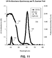
- Figure 11 is a plot 1100 including a UV-Vis absorbance spectrum 1102 and photoluminescent emission spectrum 1104 for a CdSe/CdS core/shell quantum dot having a PLQY of 96%, in accordance with an embodiment of the present invention.
- the quantum dot has essentially no overlapping absorption and emission bands.
- Figure 12 is a transmission electron microscope (TEM) image 1200 of a sample of CdSe/CdS quantum dots 1202 fabricated according to example 4, in accordance with an embodiment of the present invention.
- TEM transmission electron microscope
- Example 5 Reactive Ligand Exchange for quantum dot structures.
- 0.235g of concentration-adjusted CdSe stock from Example 2 are exposed to a reactive exchange chemical, trimethylsilylpyrollidine (TMS-Pyr), for 20 minutes in an air-free environment and are mixed completely.
- TMS-Pyr trimethylsilylpyrollidine
- an alcohol usually 2-propanol or methanol is added to the mixture to quench the reactivity of the TMS-Pyr reagent, and to precipitate the reactively exchanged CdSe particles.
- the precipitated particles are centrifuged at 6000 RPM for 5 minutes.
- the resulting supernatant liquid is decanted and the precipitate are re-dissolved in 0.235 g of anhydrous toluene for use in the procedure described in Example 2.
- Reactive ligand exchange is used to introduce any number of desired surface functionalities to the surface of quantum dot cores prior to rod growth or the surface of the core/shell particles after synthesis
- Example 7 Coating a semiconductor nanocrystal with silica using IGEPAL CO- 520. Approximately 4.46 g of Igepal CO-520 (Polyoxyethylene (5) nonylphenylether) is dissolved in 50mL of cyclohexane and allowed to mix. "n" may be 3, 4, 5, 6, 7, 8, 9 or 10, preferably about 5. 0.5 grams of quantum dots dissolved in toluene are added. 20 ⁇ L of 3-APTMS is added and stirred for about 30 minutes. 900 ⁇ L of NH 4 OH (29wt%) is added into the solution immediately followed by 600 ⁇ L of TEOS.
- IGEPAL CO- 520 Polyoxyethylene (5) nonylphenylether
- the solution is stirred for about 16hrs at 1600 rpm which allows the mixture to react until a silica shell coats the nanocrystal.
- the micelles are broken up by IPA and collected using a centrifuge.
- the SiO 2 coated particles may be re-dispersed in toluene or left in cyclohexane for polymer integration.
- Example 8 Methoxy silane coupling agent.
- the functionalized particles are separated and cleaned by precipitation with IPA and centrifugation at 6000 rpm for 10 min. The process is repeated two or more times. Cleaned particles are dispersed in a known amount of toluene or polymer solution.
- Example 9 Quantum dot/polymer preparation. To prepare the films, a known mass of quantum dots in toluene or cyclohexane is added to premade polymer solution, depending on solvent compatibility of the polymer matrix used. Other solvents may also be used for dissolution, if so desired for polarity match with the matrix or to increase or decrease the viscosity or rate of solvent evolution from the cast film.
- Example 12 In one embodiment, it is preferred that the olefin group is able to participate in a crosslinking process through radical mechanism in the case of EVA or through hydrosilylation process in the case of siloxanes. Allyl and vinyl are preferred, but other olefins can be included.
- Example 13 In one example, the degree of crosslinking may be increased using quantum dots with a higher density of the olefin groups on silica surface of quantum dots.
- Example 15 Pt catalyst.
- a platinum-based catalyst may be introduced in Examples 9-14.
- two competing or complementary catalysts are available for cross-linking.
Landscapes
- Chemical & Material Sciences (AREA)
- Engineering & Computer Science (AREA)
- Organic Chemistry (AREA)
- Materials Engineering (AREA)
- Inorganic Chemistry (AREA)
- Nanotechnology (AREA)
- Composite Materials (AREA)
- Condensed Matter Physics & Semiconductors (AREA)
- General Physics & Mathematics (AREA)
- Crystallography & Structural Chemistry (AREA)
- Physics & Mathematics (AREA)
- Luminescent Compositions (AREA)
- Led Device Packages (AREA)
- Compositions Of Macromolecular Compounds (AREA)
- Inorganic Compounds Of Heavy Metals (AREA)
Applications Claiming Priority (6)
| Application Number | Priority Date | Filing Date | Title |
|---|---|---|---|
| US201161557653P | 2011-11-09 | 2011-11-09 | |
| US201161558964P | 2011-11-11 | 2011-11-11 | |
| US201161558974P | 2011-11-11 | 2011-11-11 | |
| US13/485,761 US20130112941A1 (en) | 2011-11-09 | 2012-05-31 | Semiconductor structure having nanocrystalline core and nanocrystalline shell with insulator coating |
| PCT/US2012/055626 WO2013070321A1 (en) | 2011-11-09 | 2012-09-14 | Semiconductor structure having nanocrystalline core and nanocrystalline shell with insulator coating |
| EP12848041.5A EP2798038B1 (en) | 2011-11-09 | 2012-09-14 | Semiconductor structure having nanocrystalline core and nanocrystalline shell with insulator coating |
Related Parent Applications (2)
| Application Number | Title | Priority Date | Filing Date |
|---|---|---|---|
| EP12848041.5A Division-Into EP2798038B1 (en) | 2011-11-09 | 2012-09-14 | Semiconductor structure having nanocrystalline core and nanocrystalline shell with insulator coating |
| EP12848041.5A Division EP2798038B1 (en) | 2011-11-09 | 2012-09-14 | Semiconductor structure having nanocrystalline core and nanocrystalline shell with insulator coating |
Publications (2)
| Publication Number | Publication Date |
|---|---|
| EP3613828A1 EP3613828A1 (en) | 2020-02-26 |
| EP3613828B1 true EP3613828B1 (en) | 2021-12-15 |
Family
ID=48223094
Family Applications (7)
| Application Number | Title | Priority Date | Filing Date |
|---|---|---|---|
| EP12847998.7A Active EP2798037B1 (en) | 2011-11-09 | 2012-09-14 | Composite having semiconductor structures embedded in a matrix |
| EP12848041.5A Active EP2798038B1 (en) | 2011-11-09 | 2012-09-14 | Semiconductor structure having nanocrystalline core and nanocrystalline shell with insulator coating |
| EP21172454.7A Pending EP3879585A1 (en) | 2011-11-09 | 2012-09-14 | Semiconductor structure having nanocrystalline core and nanocrystalline shell |
| EP19153485.8A Active EP3495447B1 (en) | 2011-11-09 | 2012-09-14 | Composite having semiconductor structures embedded in a matrix |
| EP19200464.6A Active EP3613828B1 (en) | 2011-11-09 | 2012-09-14 | Semiconductor structure having nanocrystalline core and nanocrystalline shell with insulator coating |
| EP19199909.3A Active EP3613827B1 (en) | 2011-11-09 | 2012-09-14 | Semiconductor structure having nanocrystalline core and nanocrystalline shell |
| EP12847949.0A Active EP2798036B1 (en) | 2011-11-09 | 2012-09-14 | Semiconductor structure having nanocrystalline core and nanocrystalline shell |
Family Applications Before (4)
| Application Number | Title | Priority Date | Filing Date |
|---|---|---|---|
| EP12847998.7A Active EP2798037B1 (en) | 2011-11-09 | 2012-09-14 | Composite having semiconductor structures embedded in a matrix |
| EP12848041.5A Active EP2798038B1 (en) | 2011-11-09 | 2012-09-14 | Semiconductor structure having nanocrystalline core and nanocrystalline shell with insulator coating |
| EP21172454.7A Pending EP3879585A1 (en) | 2011-11-09 | 2012-09-14 | Semiconductor structure having nanocrystalline core and nanocrystalline shell |
| EP19153485.8A Active EP3495447B1 (en) | 2011-11-09 | 2012-09-14 | Composite having semiconductor structures embedded in a matrix |
Family Applications After (2)
| Application Number | Title | Priority Date | Filing Date |
|---|---|---|---|
| EP19199909.3A Active EP3613827B1 (en) | 2011-11-09 | 2012-09-14 | Semiconductor structure having nanocrystalline core and nanocrystalline shell |
| EP12847949.0A Active EP2798036B1 (en) | 2011-11-09 | 2012-09-14 | Semiconductor structure having nanocrystalline core and nanocrystalline shell |
Country Status (6)
| Country | Link |
|---|---|
| US (5) | US20130112942A1 (OSRAM) |
| EP (7) | EP2798037B1 (OSRAM) |
| JP (3) | JP2015504459A (OSRAM) |
| KR (3) | KR102009925B1 (OSRAM) |
| CN (3) | CN104024370B (OSRAM) |
| WO (3) | WO2013070320A1 (OSRAM) |
Families Citing this family (67)
| Publication number | Priority date | Publication date | Assignee | Title |
|---|---|---|---|---|
| US20110220194A1 (en) | 2009-07-14 | 2011-09-15 | Spectrawatt, Inc. | Light conversion efficiency-enhanced solar cell fabricated with downshifting nanomaterial |
| US9155497B1 (en) | 2011-06-02 | 2015-10-13 | Stc.Unm | Compact biosensor of matrix metalloproteinase with cadmium free quantum dots |
| KR101739576B1 (ko) * | 2011-10-28 | 2017-05-25 | 삼성전자주식회사 | 반도체 나노결정-고분자 미분 복합체, 이의 제조방법 및 이를 포함하는 광전자 소자 |
| US20130112941A1 (en) | 2011-11-09 | 2013-05-09 | Juanita Kurtin | Semiconductor structure having nanocrystalline core and nanocrystalline shell with insulator coating |
| US20130112942A1 (en) * | 2011-11-09 | 2013-05-09 | Juanita Kurtin | Composite having semiconductor structures embedded in a matrix |
| BR112014021766B1 (pt) * | 2012-07-11 | 2021-05-11 | Lumileds Holding B.V | produto de silicone, unidade de iluminação, e método de fabricação de um produto de silicone |
| US9425365B2 (en) | 2012-08-20 | 2016-08-23 | Pacific Light Technologies Corp. | Lighting device having highly luminescent quantum dots |
| US8889457B2 (en) | 2012-12-13 | 2014-11-18 | Pacific Light Technologies Corp. | Composition having dispersion of nano-particles therein and methods of fabricating same |
| US20140170786A1 (en) * | 2012-12-13 | 2014-06-19 | Juanita N. Kurtin | Ceramic composition having dispersion of nano-particles therein and methods of fabricating same |
| US9091655B2 (en) * | 2013-03-12 | 2015-07-28 | Pacific Light Technologies Corp. | Photoluminescence quantum yield (PLQY) test of quantum dot (QD) films |
| US9249354B2 (en) * | 2013-07-03 | 2016-02-02 | Pacific Light Technologies Corp. | Network of semiconductor structures with fused insulator coating |
| US9722147B2 (en) | 2013-07-03 | 2017-08-01 | Pacific Light Technologies Corp. | Network of semiconductor structures with fused insulator coating |
| WO2015009728A1 (en) * | 2013-07-15 | 2015-01-22 | Pacific Light Technologies Corp. | Alloyed nanocrystals and quantum dots having alloyed nanocrystals |
| US9666766B2 (en) | 2013-08-21 | 2017-05-30 | Pacific Light Technologies Corp. | Quantum dots having a nanocrystalline core, a nanocrystalline shell surrounding the core, and an insulator coating for the shell |
| US9318649B2 (en) | 2013-09-25 | 2016-04-19 | Phoseon Technology, Inc. | Multi-wavelength LED curing lamp |
| US9825205B2 (en) * | 2014-01-17 | 2017-11-21 | Pacific Light Technologies Corp. | Quantum dot (QD) polymer composites for on-chip light emitting diode (LED) applications |
| CN104211071B (zh) * | 2014-09-05 | 2015-11-11 | 哈尔滨工业大学 | 一种CdS@SiO2纳米复合材料的合成方法 |
| KR101686713B1 (ko) | 2014-12-08 | 2016-12-14 | 엘지전자 주식회사 | 양자점-고분자 복합체의 제조 방법, 양자점-고분자 복합체, 이를 포함하는 광 변환 필름, 백라이트 유닛 및 표시장치 |
| JP2016172829A (ja) * | 2015-03-17 | 2016-09-29 | コニカミノルタ株式会社 | 被覆半導体ナノ粒子およびその製造方法。 |
| US10266760B2 (en) | 2015-05-13 | 2019-04-23 | Osram Opto Semiconductors Gmbh | Composition of, and method for forming, a semiconductor structure with multiple insulator coatings |
| WO2016189869A1 (ja) * | 2015-05-28 | 2016-12-01 | 富士フイルム株式会社 | 量子ドット含有組成物、波長変換部材、バックライトユニット、および液晶表示装置 |
| US10516082B2 (en) * | 2015-07-07 | 2019-12-24 | Lumileds Holding B.V. | Device for emitting light |
| US10221356B2 (en) | 2015-07-30 | 2019-03-05 | Osram Opto Semiconductors Gmbh | Low-cadmium nanocrystalline quantum dot heterostructure |
| CN105255479B (zh) * | 2015-09-28 | 2017-06-20 | 上海皇广光电科技有限公司 | 一种胶体量子点荧光粉复合薄膜制备方法 |
| WO2017096227A1 (en) | 2015-12-02 | 2017-06-08 | Nanosys, Inc. | Quantum dot based color conversion layer in display devices |
| DE102015121720A1 (de) * | 2015-12-14 | 2017-06-14 | Osram Opto Semiconductors Gmbh | Konversionselement, optoelektronisches Bauelement und Verfahren zur Herstellung eines Konversionselements |
| KR102618409B1 (ko) | 2015-12-23 | 2023-12-27 | 삼성전자주식회사 | 양자점-폴리머 복합체 및 이를 포함하는 소자 |
| KR20180099784A (ko) * | 2015-12-31 | 2018-09-05 | 쓰리엠 이노베이티브 프로퍼티즈 컴파니 | 양자점을 포함하는 복합 입자 및 그의 제조 방법 |
| US10355175B2 (en) * | 2016-03-10 | 2019-07-16 | Panasonic Intellectual Property Management Co., Ltd. | Light emitting device |
| TWI796290B (zh) * | 2016-04-12 | 2023-03-21 | 美商羅門哈斯電子材料有限公司 | 聚合物複合物及其製造方法 |
| CN109075222B (zh) * | 2016-04-26 | 2021-09-24 | 昭荣化学工业株式会社 | 量子点材料及量子点材料的制造方法 |
| KR101841616B1 (ko) * | 2016-05-18 | 2018-03-23 | 한국과학기술원 | 반도체 나노결정 실록산 복합체 수지 조성물 및 그 제조방법 |
| EP3493922B1 (en) * | 2016-08-03 | 2021-12-22 | Lumileds LLC | Coated wavelength converting nanoparticles and method of manufacturung the same |
| US20180040783A1 (en) | 2016-08-03 | 2018-02-08 | Lumileds Llc | Coated wavelength converting nanoparticles |
| CN107760307B (zh) * | 2016-08-17 | 2021-03-02 | 苏州星烁纳米科技有限公司 | 一种量子点及其制备方法、背光模组和显示装置 |
| US10294421B2 (en) * | 2016-09-07 | 2019-05-21 | Christie Digital Systems Usa, Inc. | Core-shell quantum dots and method of synthesizing thereof |
| KR102640897B1 (ko) * | 2016-09-13 | 2024-02-26 | 엘지디스플레이 주식회사 | 양자막대, 그 합성 방법 및 양자막대 표시장치 |
| CN106353847B (zh) * | 2016-10-18 | 2020-06-23 | Tcl科技集团股份有限公司 | 一种CdSe/CdS纳米棒、偏振薄膜及其制备方法 |
| JP2020514432A (ja) * | 2016-12-15 | 2020-05-21 | メルク パテント ゲゼルシャフト ミット ベシュレンクテル ハフツングMerck Patent Gesellschaft mit beschraenkter Haftung | 半導電性発光ナノ粒子 |
| WO2018117130A1 (ja) * | 2016-12-22 | 2018-06-28 | 住友化学株式会社 | 組成物、フィルム、積層構造体、発光装置、ディスプレイ、及び組成物の製造方法 |
| KR20180093216A (ko) * | 2017-02-10 | 2018-08-21 | 엘지디스플레이 주식회사 | 형광체, 발광소자 패키지 및 전자기기 |
| CN107037012B (zh) * | 2017-04-05 | 2019-10-25 | 华中科技大学 | 用于激光诱导击穿光谱采集的阶梯光谱仪动态校正方法 |
| US10345688B2 (en) | 2017-04-18 | 2019-07-09 | Unique Materials Co., Ltd. | Light emitting apparatus using composite material |
| CN108864824A (zh) * | 2017-05-11 | 2018-11-23 | Tcl集团股份有限公司 | 量子点荧光防伪油墨及其制备方法 |
| WO2019016274A1 (de) * | 2017-07-19 | 2019-01-24 | Arras Janet | Oberflächen-funktionalisierter luminophor, zusammensetzung und gehärtete zusammensetzung umfassend dergleichen und verwendung dergleichen sowie verfahren zur herstellung eines lumineszenz-markierten artikels |
| JP6837560B2 (ja) | 2017-08-24 | 2021-03-03 | 富士フイルム株式会社 | コアシェル粒子、コアシェル粒子の製造方法およびフィルム |
| US10421904B2 (en) * | 2017-11-10 | 2019-09-24 | Osram Opto Semiconductors Gmbh | Semiconductor structure and light-emitting device with semiconductor structures |
| KR102515817B1 (ko) | 2017-11-28 | 2023-03-29 | 엘지디스플레이 주식회사 | 발광체, 이를 포함하는 발광 필름, 발광다이오드 및 발광장치 |
| US10851297B2 (en) | 2018-07-10 | 2020-12-01 | Samsung Electronics Co., Ltd. | Composition, patterned film, and electronic device including the same |
| CN111072056B (zh) * | 2018-10-22 | 2022-02-11 | 中国科学院大连化学物理研究所 | 液相CdS纳米棒尺寸控制生长方法 |
| JPWO2020085513A1 (ja) * | 2018-10-26 | 2021-11-04 | 住友化学株式会社 | 粒子、組成物、フィルム、積層構造体、発光装置及びディスプレイ |
| KR102666905B1 (ko) | 2018-10-30 | 2024-05-17 | 삼성디스플레이 주식회사 | 발광 소자 분산제, 이를 포함하는 발광 소자 잉크 및 표시 장치의 제조 방법 |
| KR102208048B1 (ko) * | 2018-11-01 | 2021-01-27 | 한국세라믹기술원 | CdSe/ZnSe 양자점/나노로드 헤테로 나노 구조체의 제조방법 |
| CN109652059A (zh) * | 2019-01-11 | 2019-04-19 | 深圳扑浪创新科技有限公司 | 一种量子点薄膜及一种氧化铝包覆量子点的制备方法 |
| US11569421B2 (en) | 2019-03-06 | 2023-01-31 | Osram Opto Semiconductors Gmbh | Semiconductor structure with nanoparticles and light emitting device having a phosphor material with nanoparticles |
| CN111718707A (zh) * | 2019-03-19 | 2020-09-29 | Tcl集团股份有限公司 | 一种颗粒及其制备方法,以及一种薄膜 |
| KR102324378B1 (ko) * | 2019-09-05 | 2021-11-10 | 연세대학교 산학협력단 | 소수성 측쇄 리간드를 갖는 반도체 나노입자-고분자 나노복합체, 이의 제조방법 및 이를 포함하는 광전자 장치 |
| KR102230527B1 (ko) * | 2019-11-04 | 2021-03-19 | 가천대학교 산학협력단 | 정렬된 유무기 복합 열전소재 및 그의 제조방법 |
| WO2021150561A2 (en) * | 2020-01-22 | 2021-07-29 | Battelle Memorial Institute | Luminescent nanoparticle tracers, and systems and methods for fabrication and use thereof |
| CN113359360A (zh) * | 2020-03-04 | 2021-09-07 | 江苏集萃智能液晶科技有限公司 | 复合粒子及包含复合粒子的调光器件 |
| KR102841608B1 (ko) | 2020-08-13 | 2025-08-01 | 삼성디스플레이 주식회사 | 발광 소자, 이의 제조 방법 및 표시 장치 |
| KR20220046066A (ko) | 2020-10-06 | 2022-04-14 | 삼성디스플레이 주식회사 | 발광 소자, 발광 소자의 제조 방법, 및 이를 포함하는 표시 장치 |
| KR102789522B1 (ko) * | 2021-05-25 | 2025-04-03 | 단국대학교 천안캠퍼스 산학협력단 | 양자점 및 이의 제조방법 |
| KR102760177B1 (ko) * | 2021-08-05 | 2025-01-24 | 한국과학기술연구원 | 표면 개질된 양자점, 이의 제조 방법, 및 이를 포함하는 양자점-폴리머 복합체 또는 전자 소자 |
| US11680200B2 (en) * | 2021-11-16 | 2023-06-20 | Saudi Arabian Oil Company | Gel fluid composites comprising nanosilica and quantum dots for sealing water production in a wellbore |
| US12291661B2 (en) * | 2021-12-22 | 2025-05-06 | Osram Opto Semiconductors Gmbh | Quantum dot structure, method for producing a quantum dot structure, and light emitting device |
| WO2024237137A1 (ja) * | 2023-05-18 | 2024-11-21 | 信越化学工業株式会社 | 量子ドット組成物、樹脂組成物、及び波長変換材料 |
Family Cites Families (176)
| Publication number | Priority date | Publication date | Assignee | Title |
|---|---|---|---|---|
| GB1308608A (en) | 1969-04-22 | 1973-02-21 | Creators Ltd | Decorative plastics strips and motifs |
| US4539049A (en) | 1983-02-09 | 1985-09-03 | Jos. Cavedon Co., Inc. | Aluminum zirconium metallo-organic complex useful as coupling and hydrophobic agents |
| US4539048A (en) | 1983-02-09 | 1985-09-03 | Jos. Cavedon Company Inc. | Aluminum zirconium metallo-organic complexes useful as coupling agents |
| US5238671A (en) | 1987-11-27 | 1993-08-24 | Battelle Memorial Institute | Chemical reactions in reverse micelle systems |
| US5760100B1 (en) | 1994-09-06 | 2000-11-14 | Ciba Vision Corp | Extended wear ophthalmic lens |
| US7125938B2 (en) | 1997-03-11 | 2006-10-24 | Carnegie Mellon University | Atom or group transfer radical polymerization |
| US6322901B1 (en) | 1997-11-13 | 2001-11-27 | Massachusetts Institute Of Technology | Highly luminescent color-selective nano-crystalline materials |
| GB9724642D0 (en) | 1997-11-21 | 1998-01-21 | British Tech Group | Single electron devices |
| US6207392B1 (en) | 1997-11-25 | 2001-03-27 | The Regents Of The University Of California | Semiconductor nanocrystal probes for biological applications and process for making and using such probes |
| US5990479A (en) * | 1997-11-25 | 1999-11-23 | Regents Of The University Of California | Organo Luminescent semiconductor nanocrystal probes for biological applications and process for making and using such probes |
| KR100593712B1 (ko) | 1998-01-22 | 2006-06-30 | 루미넥스 코포레이션 | 다수의 형광 시그널을 갖는 마이크로입자 |
| US6501091B1 (en) | 1998-04-01 | 2002-12-31 | Massachusetts Institute Of Technology | Quantum dot white and colored light emitting diodes |
| US6329058B1 (en) | 1998-07-30 | 2001-12-11 | 3M Innovative Properties Company | Nanosize metal oxide particles for producing transparent metal oxide colloids and ceramers |
| US6235864B1 (en) | 1999-05-12 | 2001-05-22 | Sandia Corporation | Non-strinking siloxane polymers |
| US6225198B1 (en) | 2000-02-04 | 2001-05-01 | The Regents Of The University Of California | Process for forming shaped group II-VI semiconductor nanocrystals, and product formed using process |
| US6437234B1 (en) | 2000-07-27 | 2002-08-20 | Kyocera Corporation | Photoelectric conversion device and manufacturing method thereof |
| EP1412413B1 (en) | 2001-06-29 | 2011-08-10 | Nanomics Biosystems Pty, Ltd. | Synthesis and use of organosilica particles |
| US20050049381A1 (en) | 2001-07-05 | 2005-03-03 | Mikio Yamahiro | Silicon compounds |
| US6656990B2 (en) | 2001-07-11 | 2003-12-02 | Corning Incorporated | Curable high refractive index compositions |
| US20030060547A1 (en) * | 2001-07-24 | 2003-03-27 | Chi-Ming Chan | Polypropylene/calcium carbonate nanocomposites |
| US20030066998A1 (en) * | 2001-08-02 | 2003-04-10 | Lee Howard Wing Hoon | Quantum dots of Group IV semiconductor materials |
| US7214428B2 (en) * | 2001-09-17 | 2007-05-08 | Invitrogen Corporation | Highly luminescent functionalized semiconductor nanocrystals for biological and physical applications |
| US6951672B2 (en) | 2002-03-12 | 2005-10-04 | Hewlett-Packard Development Company, L.P. | Chemically-modified coatings for enhanced performance of ink-jet images |
| FR2838241B1 (fr) * | 2002-04-09 | 2004-06-25 | Commissariat Energie Atomique | Materiaux luminescents constitues de nanocristaux a structure coeur/coquille et leur procede de preparation |
| US6788453B2 (en) * | 2002-05-15 | 2004-09-07 | Yissum Research Development Company Of The Hebrew Univeristy Of Jerusalem | Method for producing inorganic semiconductor nanocrystalline rods and their use |
| US7515333B1 (en) | 2002-06-13 | 2009-04-07 | Nanosy's, Inc. | Nanotechnology-enabled optoelectronics |
| JP2006513458A (ja) * | 2002-08-02 | 2006-04-20 | ウルトラドッツ・インコーポレイテッド | 量子ドット、量子ドットを持つナノ複合材料、量子ドットを持つ光学デバイス、および関連した製造方法 |
| US7068898B2 (en) | 2002-09-05 | 2006-06-27 | Nanosys, Inc. | Nanocomposites |
| WO2004023527A2 (en) | 2002-09-05 | 2004-03-18 | Nanosys, Inc. | Nanostructure and nanocomposite based compositions and photovoltaic devices |
| US7534488B2 (en) | 2003-09-10 | 2009-05-19 | The Regents Of The University Of California | Graded core/shell semiconductor nanorods and nanorod barcodes |
| US20040101822A1 (en) | 2002-11-26 | 2004-05-27 | Ulrich Wiesner | Fluorescent silica-based nanoparticles |
| EP1590171B1 (en) | 2003-01-22 | 2011-06-08 | The Board Of Trustees Of The University Of Arkansas | Monodisperse core/shell and other complex structured nanocrystals and methods of preparing the same |
| WO2005022120A2 (en) * | 2003-03-11 | 2005-03-10 | Nanosys, Inc. | Process for producing nanocrystals and nanocrystals produced thereby |
| ATE346898T1 (de) | 2003-04-30 | 2006-12-15 | Nanosolutions Gmbh | Kern-mantel nanoteilchen für (f) ret- testverfahren |
| EP2530719B1 (en) | 2003-05-07 | 2020-08-05 | Indiana University Research and Technology Corporation | Alloyed semiconductor concentration-gradient quantum dots, use and method of fabricating thereof |
| CN1312479C (zh) * | 2003-08-08 | 2007-04-25 | 清华大学 | 一种纳米荧光磁粒及其制备方法 |
| US7065285B2 (en) | 2003-12-01 | 2006-06-20 | Lucent Technologies Inc. | Polymeric compositions comprising quantum dots, optical devices comprising these compositions and methods for preparing same |
| CA2550153A1 (en) | 2003-12-12 | 2005-07-28 | Quantum Dot Corporation | Preparation of stable, bright luminescent nanoparticles having compositionally engineered properties |
| EP1733077B1 (en) | 2004-01-15 | 2018-04-18 | Samsung Electronics Co., Ltd. | Nanocrystal doped matrixes |
| US7645397B2 (en) | 2004-01-15 | 2010-01-12 | Nanosys, Inc. | Nanocrystal doped matrixes |
| US20050230673A1 (en) | 2004-03-25 | 2005-10-20 | Mueller Alexander H | Colloidal quantum dot light emitting diodes |
| GB0409877D0 (en) | 2004-04-30 | 2004-06-09 | Univ Manchester | Preparation of nanoparticle materials |
| US20060088713A1 (en) | 2004-05-05 | 2006-04-27 | Dykstra Tieneke E | Surface modification of nanocrystals using multidentate polymer ligands |
| US7229690B2 (en) | 2004-07-26 | 2007-06-12 | Massachusetts Institute Of Technology | Microspheres including nanoparticles |
| US7405002B2 (en) | 2004-08-04 | 2008-07-29 | Agency For Science, Technology And Research | Coated water-soluble nanoparticles comprising semiconductor core and silica coating |
| US20060083694A1 (en) * | 2004-08-07 | 2006-04-20 | Cabot Corporation | Multi-component particles comprising inorganic nanoparticles distributed in an organic matrix and processes for making and using same |
| US20080296534A1 (en) * | 2004-09-09 | 2008-12-04 | Technion Research And Development Foundation Ltd. | Core-Alloyed Shell Semiconductor Nanocrystals |
| JP2006083219A (ja) * | 2004-09-14 | 2006-03-30 | Sharp Corp | 蛍光体およびこれを用いた発光装置 |
| US7857993B2 (en) | 2004-09-14 | 2010-12-28 | Ut-Battelle, Llc | Composite scintillators for detection of ionizing radiation |
| EP2292718A3 (en) | 2004-11-11 | 2011-06-22 | Samsung Electronics Co., Ltd | Interfused nanocrystals and method of preparing the same |
| JP2008520799A (ja) | 2004-11-19 | 2008-06-19 | エージェンシー フォー サイエンス,テクノロジー アンド リサーチ | 水溶液中でのコア/シェル型半導体ナノ結晶の生成 |
| KR100682928B1 (ko) | 2005-02-03 | 2007-02-15 | 삼성전자주식회사 | 양자점 화합물을 포함하는 에너지 변환막 및 양자점 박막 |
| US7632428B2 (en) | 2005-04-25 | 2009-12-15 | The Board Of Trustees Of The University Of Arkansas | Doped semiconductor nanocrystals and methods of making same |
| US8084001B2 (en) | 2005-05-02 | 2011-12-27 | Cornell Research Foundation, Inc. | Photoluminescent silica-based sensors and methods of use |
| CN101194164A (zh) | 2005-06-07 | 2008-06-04 | 皇家飞利浦电子股份有限公司 | 活体表达谱 |
| CN100570912C (zh) | 2005-06-15 | 2009-12-16 | 耶路撒冷希伯来大学伊萨姆研发公司 | Ⅲ-ⅴ半导体核-异质壳纳米晶体 |
| KR101159853B1 (ko) | 2005-09-12 | 2012-06-25 | 삼성전기주식회사 | 다층구조 나노결정의 제조방법 및 그에 의해 수득된 나노결정 |
| US8337721B2 (en) | 2005-12-02 | 2012-12-25 | Vanderbilt University | Broad-emission nanocrystals and methods of making and using same |
| KR20080081180A (ko) * | 2005-12-21 | 2008-09-08 | 더 리서치 파운데이션 오브 스테이트 유니버시티 오브 뉴욕 | 비구형 반도체 나노결정 및 그의 제조 방법 |
| US7394094B2 (en) | 2005-12-29 | 2008-07-01 | Massachusetts Institute Of Technology | Semiconductor nanocrystal heterostructures |
| WO2007095173A2 (en) * | 2006-02-14 | 2007-08-23 | Massachusetts Institute Of Technology | White light emitting devices |
| KR100745745B1 (ko) | 2006-02-21 | 2007-08-02 | 삼성전기주식회사 | 나노복합재료 및 그 제조방법 |
| WO2007103802A2 (en) | 2006-03-03 | 2007-09-13 | William Marsh Rice University | Nanorice particles: hybrid plasmonic nanostructures |
| WO2008070028A2 (en) | 2006-12-01 | 2008-06-12 | Qd Vision, Inc. | Improved composites and devices including nanoparticles |
| FR2898519B1 (fr) | 2006-03-20 | 2009-01-09 | Commissariat Energie Atomique | Nanoparticules notamment a structure coeur coquilles, enrobees |
| DE602006018532D1 (de) | 2006-03-24 | 2011-01-05 | Postech Acad Ind Found | Stationäre phase und säule unter verwendung von cucurbiturilgebundenem kieselgel, und verfahren zur abtrennung von taxol unter verwendung der säule |
| US20080038558A1 (en) | 2006-04-05 | 2008-02-14 | Evident Technologies, Inc. | I-iii-vi semiconductor nanocrystals, i-iii-vi water stable semiconductor nanocrystals, and methods of making same |
| US7693369B2 (en) | 2006-04-07 | 2010-04-06 | The Curators Of The University Of Missouri | Hollow core optical ring resonator sensor, sensing methods, and methods of fabrication |
| US8050303B2 (en) | 2006-04-12 | 2011-11-01 | Raytheon Company | Laser based on quantum dot activated media with forster resonant energy transfer excitation |
| JP4568862B2 (ja) * | 2006-04-14 | 2010-10-27 | 独立行政法人産業技術総合研究所 | コアシェル型粒子及びその製造方法 |
| US20080003694A1 (en) | 2006-04-18 | 2008-01-03 | Swanson Basil I | Robust, self-assembled, biocompatible films |
| KR100819337B1 (ko) | 2006-06-14 | 2008-04-02 | 재단법인서울대학교산학협력재단 | 양자점을 이용한 백색광 led 구조 및 그 제조 방법 |
| US8178202B2 (en) | 2006-06-21 | 2012-05-15 | William Marsh Rice University | Nonconcentric nanoshells with offset core in relation to shell and method of using the same |
| KR101290251B1 (ko) * | 2006-08-21 | 2013-07-30 | 삼성전자주식회사 | 복합 발광 재료 및 그를 포함하는 발광 소자 |
| WO2008063653A1 (en) * | 2006-11-21 | 2008-05-29 | Qd Vision, Inc. | Semiconductor nanocrystals and compositions and devices including same |
| WO2008063652A1 (en) | 2006-11-21 | 2008-05-29 | Qd Vision, Inc. | Blue emitting semiconductor nanocrystals and compositions and devices including same |
| US8491818B2 (en) | 2006-11-27 | 2013-07-23 | Drexel University | Synthesis of water soluble non-toxic nanocrystalline quantum dots and uses thereof |
| US7933022B2 (en) | 2006-12-01 | 2011-04-26 | 3M Innovative Properties Company | Integrated optical disk resonator |
| DE102006060366B8 (de) | 2006-12-16 | 2013-08-01 | Helmholtz-Zentrum Berlin Für Materialien Und Energie Gmbh | Verfahren zur Herstellung von von einer Matrix abgedeckten Quantenpunkten |
| US20080199510A1 (en) | 2007-02-20 | 2008-08-21 | Xtent, Inc. | Thermo-mechanically controlled implants and methods of use |
| US20080237540A1 (en) * | 2007-03-19 | 2008-10-02 | Nanosys, Inc. | Methods for encapsulating nanocrystals |
| US8618528B2 (en) | 2007-03-20 | 2013-12-31 | Samsung Electronics Co., Ltd. | Quantum dot particles on the micron or nanometer scale and method of making the same |
| KR100841186B1 (ko) | 2007-03-26 | 2008-06-24 | 삼성전자주식회사 | 다층 쉘 구조의 나노결정 및 그의 제조방법 |
| US7892739B2 (en) | 2007-03-27 | 2011-02-22 | Lehigh University | Systems, compositions and methods for nucleic acid detection |
| US20080237541A1 (en) | 2007-03-30 | 2008-10-02 | General Electric Company | Thermo-optically functional compositions, systems and methods of making |
| WO2009025913A2 (en) | 2007-05-31 | 2009-02-26 | Invitrogen Corporation | Magnesium-based coatings for nanocrystals |
| KR20080107578A (ko) | 2007-06-07 | 2008-12-11 | 삼성전자주식회사 | 코어/쉘 나노결정 및 그 제조방법 |
| US8399751B2 (en) | 2007-06-12 | 2013-03-19 | University Of Southern California | Functional abiotic nanosystems |
| JP2010535692A (ja) | 2007-08-06 | 2010-11-25 | エージェンシー フォー サイエンス,テクノロジー アンド リサーチ | カドミウムおよびセレン含有ナノ結晶複合材料を形成する方法ならびに該方法から得られるナノ結晶複合材料 |
| WO2009026141A1 (en) | 2007-08-17 | 2009-02-26 | University Of Florida Research Foundation, Inc. | Supercrystalline colloidal particles and method of production |
| JP2009087744A (ja) | 2007-09-28 | 2009-04-23 | Dainippon Printing Co Ltd | 発光素子 |
| JP5407242B2 (ja) | 2007-09-28 | 2014-02-05 | 大日本印刷株式会社 | エレクトロルミネッセンス素子 |
| JP2009087783A (ja) * | 2007-09-28 | 2009-04-23 | Dainippon Printing Co Ltd | エレクトロルミネッセンス素子 |
| JP2009087781A (ja) * | 2007-09-28 | 2009-04-23 | Dainippon Printing Co Ltd | エレクトロルミネッセンス素子およびその製造方法 |
| US20100289003A1 (en) * | 2007-10-29 | 2010-11-18 | Kahen Keith B | Making colloidal ternary nanocrystals |
| US7777233B2 (en) | 2007-10-30 | 2010-08-17 | Eastman Kodak Company | Device containing non-blinking quantum dots |
| US9662389B2 (en) | 2008-03-31 | 2017-05-30 | Duke University | Functionalized metal-coated energy converting nanoparticles, methods for production thereof and methods for use |
| US7687800B1 (en) | 2007-11-23 | 2010-03-30 | University Of Central Florida Research Foundation, Inc. | Excitation band-gap tuning of dopant based quantum dots with core-inner shell-outer shell |
| KR101460395B1 (ko) * | 2007-12-13 | 2014-11-21 | 테크니온 리서치 엔드 디벨로프먼트 화운데이션 엘티디. | 4-6족 반도체 코어-쉘 나노결정을 포함하는 광기전 셀 |
| WO2009094160A2 (en) | 2008-01-23 | 2009-07-30 | Massachusetts Institute Of Technology | Semiconductor nanocrystals |
| US20110189102A1 (en) | 2008-02-08 | 2011-08-04 | Kairdolf Brad A | Coated quantum dots and methods of making and using thereof |
| US8617707B2 (en) | 2008-03-24 | 2013-12-31 | University Of Rochester | Magic size nanoclusters and methods of preparing same |
| WO2009123734A1 (en) | 2008-04-04 | 2009-10-08 | The Regents Of The University Of California | Functionalized magnetic nanoparticles and methods of use thereof |
| EP2110414A1 (de) | 2008-04-18 | 2009-10-21 | Nanoresins AG | Oberflächenmodifizierte Siliziumdioxid-Partikel |
| GB0808153D0 (en) | 2008-05-03 | 2008-06-11 | Eastman Kodak Co | Solar concentrator |
| US8012860B2 (en) | 2008-06-17 | 2011-09-06 | Uchicago Argonne, Llc | Atomic layer deposition for functionalizing colloidal and semiconductor particles |
| KR100973172B1 (ko) | 2008-08-05 | 2010-08-02 | 한국과학기술연구원 | 단일 활성층 구조를 가지는 교류 구동형 발광소자 및 그제조방법 |
| JP5243203B2 (ja) | 2008-08-20 | 2013-07-24 | 富士フイルム株式会社 | 複合金属ナノロッド、並びに複合金属ナノロッド含有組成物、及び偏光材料 |
| JP4881358B2 (ja) * | 2008-08-28 | 2012-02-22 | 株式会社東芝 | 発光装置 |
| KR100982990B1 (ko) | 2008-09-03 | 2010-09-17 | 삼성엘이디 주식회사 | 파장변환플레이트 및 이를 이용한 발광장치 |
| JP5015891B2 (ja) | 2008-10-02 | 2012-08-29 | 信越化学工業株式会社 | 金属酸化物含有膜形成用組成物、金属酸化物含有膜形成基板及びパターン形成方法 |
| DE102008052043A1 (de) | 2008-10-16 | 2010-04-22 | Fraunhofer-Gesellschaft zur Förderung der angewandten Forschung e.V. | Fluoreszenz-Kollektor und dessen Verwendung |
| AU2009308162B2 (en) | 2008-10-24 | 2015-07-09 | Life Technologies Corporation | Stable nanoparticles and methods of making and using such particles |
| GB0821122D0 (en) | 2008-11-19 | 2008-12-24 | Nanoco Technologies Ltd | Semiconductor nanoparticle - based light emitting devices and associated materials and methods |
| JP5483669B2 (ja) * | 2008-11-26 | 2014-05-07 | 昭和電工株式会社 | 液状硬化性樹脂組成物、ナノ粒子蛍光体を含む硬化樹脂の製造方法、発光装置の製造方法、発光装置及び照明装置 |
| CN101735632B (zh) | 2008-11-26 | 2012-05-30 | 清华大学 | 纳米复合粒子及其制备方法 |
| JP4936338B2 (ja) | 2008-12-26 | 2012-05-23 | シャープ株式会社 | 半導体ナノ粒子蛍光体 |
| US8343575B2 (en) | 2008-12-30 | 2013-01-01 | Nanosys, Inc. | Methods for encapsulating nanocrystals and resulting compositions |
| EP2210616A1 (en) | 2009-01-21 | 2010-07-28 | Centre National de la Recherche Scientifique | Multifunctional stealth nanoparticles for biomedical use |
| WO2010107720A2 (en) | 2009-03-18 | 2010-09-23 | Tuan Vo-Dinh | Up and down conversion systems for production of emitted light from various energy sources |
| US20110049442A1 (en) | 2009-03-31 | 2011-03-03 | Schreuder Michael A | Surface structures for enhancement of quantum yield in broad spectrum emission nanocrystals |
| EP2414278B1 (en) | 2009-04-03 | 2019-11-27 | University Of Houston | Metal nanoparticles functionalized with rationally designed coatings |
| US8283412B2 (en) | 2009-05-01 | 2012-10-09 | Nanosys, Inc. | Functionalized matrices for dispersion of nanostructures |
| WO2010129887A2 (en) * | 2009-05-07 | 2010-11-11 | Massachusetts Institute Of Technology | Light emitting device including semiconductor nanocrystals |
| US20100288344A1 (en) | 2009-05-14 | 2010-11-18 | Photonic Glass Corporation | Methods and apparatus for wavelength conversion in solar cells and solar cell covers |
| WO2011002509A1 (en) | 2009-06-30 | 2011-01-06 | Tiecheng Alex Qiao | Semiconductor nanocrystals used with led sources |
| JP5035472B2 (ja) | 2009-07-06 | 2012-09-26 | トヨタ自動車株式会社 | 光電変換素子 |
| US20110220194A1 (en) * | 2009-07-14 | 2011-09-15 | Spectrawatt, Inc. | Light conversion efficiency-enhanced solar cell fabricated with downshifting nanomaterial |
| JP2011040486A (ja) * | 2009-08-07 | 2011-02-24 | Sharp Corp | 発光装置および画像表示装置 |
| GB0916699D0 (en) | 2009-09-23 | 2009-11-04 | Nanoco Technologies Ltd | Semiconductor nanoparticle-based materials |
| GB0916700D0 (en) | 2009-09-23 | 2009-11-04 | Nanoco Technologies Ltd | Semiconductor nanoparticle-based materials |
| JP2013511157A (ja) | 2009-11-16 | 2013-03-28 | エモリー ユニバーシティ | 格子不整合コア・シェル量子ドット |
| US20110175030A1 (en) | 2010-01-15 | 2011-07-21 | Xiaofan Ren | Preparing large-sized emitting colloidal nanocrystals |
| JP5388357B2 (ja) | 2010-01-27 | 2014-01-15 | 株式会社栄光 | 太陽光発電装置 |
| EP2528989B1 (en) * | 2010-01-28 | 2015-03-04 | Yissum Research and Development Company of The Hebrew University of Jerusalem | Phosphor-nanoparticle combinations |
| KR101744904B1 (ko) * | 2010-03-22 | 2017-06-21 | 삼성디스플레이 주식회사 | 양자점-블록공중합체 하이브리드 및 이의 제조 방법과 분산 방법, 그리고 양자점 블록공중합체 하이브리드를 포함하는 발광 소자 및 이의 제조 방법 |
| US8557329B2 (en) | 2010-05-06 | 2013-10-15 | International Business Machines Corporation | Method for silica encapsulation of magnetic particles |
| KR101738551B1 (ko) | 2010-06-24 | 2017-05-23 | 삼성전자주식회사 | 반도체 나노 결정 |
| US20120064134A1 (en) | 2010-08-06 | 2012-03-15 | Immunolight, Llc | Color enhancement utilizing up converters and down converters |
| WO2012018649A2 (en) | 2010-08-06 | 2012-02-09 | Spectrawatt, Inc. | Cooperative photovoltaic networks and photovoltaic cell adaptations for use therein |
| US10174243B2 (en) | 2010-08-24 | 2019-01-08 | Massachusetts Institute Of Technology | Highly luminescent semiconductor nanocrystals |
| KR101978691B1 (ko) * | 2010-09-16 | 2019-05-15 | 이섬 리서치 디벨러프먼트 컴파니 오브 더 히브루 유니버시 티 오브 예루살렘 엘티디. | 이방성 반도체 나노입자 |
| US20120103404A1 (en) | 2010-10-15 | 2012-05-03 | Los Alamos National Security, Llc | Quantum dot sensitized solar cell |
| US9529228B2 (en) | 2010-11-05 | 2016-12-27 | Yissum Research Development Company Of The Hebrew University Of Jerusalem, Ltd. | Polarizing lighting systems |
| US9525092B2 (en) | 2010-11-05 | 2016-12-20 | Pacific Light Technologies Corp. | Solar module employing quantum luminescent lateral transfer concentrator |
| EP3396032B1 (en) * | 2010-12-28 | 2021-02-24 | Life Technologies Corporation | Preparation of nanocrystals with mixtures of organic ligands |
| EP2472612A1 (en) | 2010-12-29 | 2012-07-04 | Koninklijke Philips Electronics N.V. | Improved angular color performance of white LED lighting systems |
| EP4245347A3 (en) | 2011-01-17 | 2023-12-06 | University of Utah Research Foundation | Apparatus and methods for reducing frequency or severity of photophobic responses or modulating circadian cycles |
| JP5647028B2 (ja) | 2011-02-14 | 2014-12-24 | スタンレー電気株式会社 | 発光装置およびその製造方法 |
| KR101223671B1 (ko) | 2011-02-19 | 2013-01-17 | 충남대학교산학협력단 | 양자점 나노입자가 분산된 에폭시 고분자 복합체 제조방법 |
| US8803412B2 (en) | 2011-03-18 | 2014-08-12 | Abl Ip Holding Llc | Semiconductor lamp |
| WO2012135744A2 (en) | 2011-04-01 | 2012-10-04 | Kai Su | White light-emitting device |
| US9267889B1 (en) | 2011-10-12 | 2016-02-23 | Stc.Unm | High efficiency light absorbing and light emitting nanostructures |
| US20130112942A1 (en) | 2011-11-09 | 2013-05-09 | Juanita Kurtin | Composite having semiconductor structures embedded in a matrix |
| US20130112941A1 (en) | 2011-11-09 | 2013-05-09 | Juanita Kurtin | Semiconductor structure having nanocrystalline core and nanocrystalline shell with insulator coating |
| US20150278919A1 (en) | 2012-05-17 | 2015-10-01 | Wal-Mart Stores, Inc. | Systems and Methods for a Catalog of Trending and Trusted Items |
| US9425365B2 (en) | 2012-08-20 | 2016-08-23 | Pacific Light Technologies Corp. | Lighting device having highly luminescent quantum dots |
| US20140117311A1 (en) | 2012-10-29 | 2014-05-01 | Juanita N. Kurtin | Semiconductor structure having nanocrystalline core and nanocrystalline shell pairing with compositional transition layer |
| US8889457B2 (en) | 2012-12-13 | 2014-11-18 | Pacific Light Technologies Corp. | Composition having dispersion of nano-particles therein and methods of fabricating same |
| US9187692B2 (en) | 2013-03-12 | 2015-11-17 | Pacific Light Technologies Corp. | Nano-crystalline core and nano-crystalline shell pairing having group I-III-VI material nano-crystalline core |
| US20140264257A1 (en) | 2013-03-12 | 2014-09-18 | Steven M. Hughes | Group i-iii-vi material nano-crystalline core and group i-iii-vi material nano-crystalline shell pairing |
| US9091655B2 (en) | 2013-03-12 | 2015-07-28 | Pacific Light Technologies Corp. | Photoluminescence quantum yield (PLQY) test of quantum dot (QD) films |
| US9443998B2 (en) | 2013-03-14 | 2016-09-13 | Nanoco Technologies Ltd. | Multi-layer-coated quantum dot beads |
| US10030851B2 (en) | 2013-03-20 | 2018-07-24 | Lumileds Llc | Encapsulated quantum dots in porous particles |
| JP6314981B2 (ja) | 2013-06-25 | 2018-04-25 | コニカミノルタ株式会社 | 光学材料、光学フィルム及び発光デバイス |
| US9249354B2 (en) | 2013-07-03 | 2016-02-02 | Pacific Light Technologies Corp. | Network of semiconductor structures with fused insulator coating |
| US9722147B2 (en) | 2013-07-03 | 2017-08-01 | Pacific Light Technologies Corp. | Network of semiconductor structures with fused insulator coating |
| WO2015009728A1 (en) | 2013-07-15 | 2015-01-22 | Pacific Light Technologies Corp. | Alloyed nanocrystals and quantum dots having alloyed nanocrystals |
| US10106734B2 (en) | 2014-07-30 | 2018-10-23 | Osram Opto Semiconductor Gmbh | Alloyed rod structure in a nanocrystalline quantum dot |
| JP6428194B2 (ja) | 2014-11-21 | 2018-11-28 | 日亜化学工業株式会社 | 波長変換部材及びその製造方法ならびに発光装置 |
| US9831397B2 (en) | 2015-03-09 | 2017-11-28 | Pacific Light Technologies Corp. | Quantum dots with multiple insulator coatings |
| CN107849438B (zh) | 2015-05-13 | 2020-05-15 | 欧司朗光电半导体有限公司 | 具有多个绝缘涂层的半导体结构的组合物和形成方法 |
| WO2017004145A1 (en) | 2015-06-30 | 2017-01-05 | Cree, Inc. | Stabilized quantum dot structure and method of making a stabilized quantum dot structure |
| US9732274B2 (en) | 2015-07-02 | 2017-08-15 | Pacific Light Technologies Corp. | Nanocrystalline quantum dot heterostructure |
| US20170271563A1 (en) | 2016-03-15 | 2017-09-21 | Chris Durgan | Method and apparatus for controlled semiconductor growth during synthesis of quantum dot materials |
| US20180166596A1 (en) | 2016-05-24 | 2018-06-14 | United States Of America, As Represented By The Secretary Of The Navy | Photo-Controllable Composite Dielectric Material |
-
2012
- 2012-05-31 US US13/485,762 patent/US20130112942A1/en not_active Abandoned
- 2012-09-14 JP JP2014541053A patent/JP2015504459A/ja active Pending
- 2012-09-14 CN CN201280065164.1A patent/CN104024370B/zh active Active
- 2012-09-14 JP JP2014541054A patent/JP2014534322A/ja active Pending
- 2012-09-14 EP EP12847998.7A patent/EP2798037B1/en active Active
- 2012-09-14 EP EP12848041.5A patent/EP2798038B1/en active Active
- 2012-09-14 JP JP2014541055A patent/JP6161620B2/ja active Active
- 2012-09-14 WO PCT/US2012/055625 patent/WO2013070320A1/en not_active Ceased
- 2012-09-14 KR KR1020147015628A patent/KR102009925B1/ko active Active
- 2012-09-14 EP EP21172454.7A patent/EP3879585A1/en active Pending
- 2012-09-14 EP EP19153485.8A patent/EP3495447B1/en active Active
- 2012-09-14 EP EP19200464.6A patent/EP3613828B1/en active Active
- 2012-09-14 EP EP19199909.3A patent/EP3613827B1/en active Active
- 2012-09-14 KR KR1020147015626A patent/KR20140109377A/ko not_active Ceased
- 2012-09-14 WO PCT/US2012/055623 patent/WO2013070319A1/en not_active Ceased
- 2012-09-14 EP EP12847949.0A patent/EP2798036B1/en active Active
- 2012-09-14 KR KR1020147015625A patent/KR102009927B1/ko active Active
- 2012-09-14 CN CN201280064403.1A patent/CN104302729A/zh active Pending
- 2012-09-14 CN CN201280065133.6A patent/CN104066813A/zh active Pending
- 2012-09-14 WO PCT/US2012/055626 patent/WO2013070321A1/en not_active Ceased
-
2015
- 2015-04-13 US US14/685,570 patent/US9793446B2/en active Active
-
2016
- 2016-01-22 US US15/004,478 patent/US10074780B2/en active Active
-
2018
- 2018-08-01 US US16/052,515 patent/US11205741B2/en active Active
-
2021
- 2021-11-10 US US17/523,828 patent/US12107197B2/en active Active
Also Published As
Similar Documents
| Publication | Publication Date | Title |
|---|---|---|
| US12107197B2 (en) | Method for forming a composite having semiconductor structures including a nanocrystalline core and shell embedded in a matrix | |
| US9153734B2 (en) | Semiconductor structure having nanocrystalline core and nanocrystalline shell | |
| US10763400B2 (en) | Quantum dots having a nanocrystalline core, a nanocrystalline shell surrounding the core, and an insulator coating for the shell | |
| US9425365B2 (en) | Lighting device having highly luminescent quantum dots | |
| US9428691B2 (en) | Semiconductor structure having nanocrystalline core and nanocrystalline shell pairing with compositional transition layer | |
| US20160230088A1 (en) | Alloyed nanocrystals and quantum dots having alloyed nanocrystals |
Legal Events
| Date | Code | Title | Description |
|---|---|---|---|
| PUAI | Public reference made under article 153(3) epc to a published international application that has entered the european phase |
Free format text: ORIGINAL CODE: 0009012 |
|
| STAA | Information on the status of an ep patent application or granted ep patent |
Free format text: STATUS: REQUEST FOR EXAMINATION WAS MADE |
|
| 17P | Request for examination filed |
Effective date: 20190930 |
|
| AC | Divisional application: reference to earlier application |
Ref document number: 2798038 Country of ref document: EP Kind code of ref document: P |
|
| AK | Designated contracting states |
Kind code of ref document: A1 Designated state(s): AL AT BE BG CH CY CZ DE DK EE ES FI FR GB GR HR HU IE IS IT LI LT LU LV MC MK MT NL NO PL PT RO RS SE SI SK SM TR |
|
| RIN1 | Information on inventor provided before grant (corrected) |
Inventor name: PARK, OUN-HO Inventor name: REESE, COLIN Inventor name: THEOBALD, BRIAN Inventor name: KURTIN, JUANITA N. Inventor name: MASSON, GEORGETA Inventor name: CARILLO, MATTHEW J Inventor name: HUGHES, STEVEN |
|
| GRAP | Despatch of communication of intention to grant a patent |
Free format text: ORIGINAL CODE: EPIDOSNIGR1 |
|
| STAA | Information on the status of an ep patent application or granted ep patent |
Free format text: STATUS: GRANT OF PATENT IS INTENDED |
|
| GRAJ | Information related to disapproval of communication of intention to grant by the applicant or resumption of examination proceedings by the epo deleted |
Free format text: ORIGINAL CODE: EPIDOSDIGR1 |
|
| STAA | Information on the status of an ep patent application or granted ep patent |
Free format text: STATUS: REQUEST FOR EXAMINATION WAS MADE |
|
| INTG | Intention to grant announced |
Effective date: 20210519 |
|
| INTC | Intention to grant announced (deleted) | ||
| GRAP | Despatch of communication of intention to grant a patent |
Free format text: ORIGINAL CODE: EPIDOSNIGR1 |
|
| STAA | Information on the status of an ep patent application or granted ep patent |
Free format text: STATUS: GRANT OF PATENT IS INTENDED |
|
| INTG | Intention to grant announced |
Effective date: 20210921 |
|
| GRAS | Grant fee paid |
Free format text: ORIGINAL CODE: EPIDOSNIGR3 |
|
| GRAA | (expected) grant |
Free format text: ORIGINAL CODE: 0009210 |
|
| STAA | Information on the status of an ep patent application or granted ep patent |
Free format text: STATUS: THE PATENT HAS BEEN GRANTED |
|
| AC | Divisional application: reference to earlier application |
Ref document number: 2798038 Country of ref document: EP Kind code of ref document: P |
|
| AK | Designated contracting states |
Kind code of ref document: B1 Designated state(s): AL AT BE BG CH CY CZ DE DK EE ES FI FR GB GR HR HU IE IS IT LI LT LU LV MC MK MT NL NO PL PT RO RS SE SI SK SM TR |
|
| REG | Reference to a national code |
Ref country code: GB Ref legal event code: FG4D Ref country code: CH Ref legal event code: EP |
|
| REG | Reference to a national code |
Ref country code: IE Ref legal event code: FG4D Ref country code: DE Ref legal event code: R096 Ref document number: 602012077397 Country of ref document: DE |
|
| REG | Reference to a national code |
Ref country code: AT Ref legal event code: REF Ref document number: 1455505 Country of ref document: AT Kind code of ref document: T Effective date: 20220115 |
|
| REG | Reference to a national code |
Ref country code: LT Ref legal event code: MG9D |
|
| REG | Reference to a national code |
Ref country code: NL Ref legal event code: MP Effective date: 20211215 |
|
| PG25 | Lapsed in a contracting state [announced via postgrant information from national office to epo] |
Ref country code: RS Free format text: LAPSE BECAUSE OF FAILURE TO SUBMIT A TRANSLATION OF THE DESCRIPTION OR TO PAY THE FEE WITHIN THE PRESCRIBED TIME-LIMIT Effective date: 20211215 Ref country code: LT Free format text: LAPSE BECAUSE OF FAILURE TO SUBMIT A TRANSLATION OF THE DESCRIPTION OR TO PAY THE FEE WITHIN THE PRESCRIBED TIME-LIMIT Effective date: 20211215 Ref country code: FI Free format text: LAPSE BECAUSE OF FAILURE TO SUBMIT A TRANSLATION OF THE DESCRIPTION OR TO PAY THE FEE WITHIN THE PRESCRIBED TIME-LIMIT Effective date: 20211215 Ref country code: BG Free format text: LAPSE BECAUSE OF FAILURE TO SUBMIT A TRANSLATION OF THE DESCRIPTION OR TO PAY THE FEE WITHIN THE PRESCRIBED TIME-LIMIT Effective date: 20220315 |
|
| REG | Reference to a national code |
Ref country code: AT Ref legal event code: MK05 Ref document number: 1455505 Country of ref document: AT Kind code of ref document: T Effective date: 20211215 |
|
| PG25 | Lapsed in a contracting state [announced via postgrant information from national office to epo] |
Ref country code: SE Free format text: LAPSE BECAUSE OF FAILURE TO SUBMIT A TRANSLATION OF THE DESCRIPTION OR TO PAY THE FEE WITHIN THE PRESCRIBED TIME-LIMIT Effective date: 20211215 Ref country code: NO Free format text: LAPSE BECAUSE OF FAILURE TO SUBMIT A TRANSLATION OF THE DESCRIPTION OR TO PAY THE FEE WITHIN THE PRESCRIBED TIME-LIMIT Effective date: 20220315 Ref country code: LV Free format text: LAPSE BECAUSE OF FAILURE TO SUBMIT A TRANSLATION OF THE DESCRIPTION OR TO PAY THE FEE WITHIN THE PRESCRIBED TIME-LIMIT Effective date: 20211215 Ref country code: HR Free format text: LAPSE BECAUSE OF FAILURE TO SUBMIT A TRANSLATION OF THE DESCRIPTION OR TO PAY THE FEE WITHIN THE PRESCRIBED TIME-LIMIT Effective date: 20211215 Ref country code: GR Free format text: LAPSE BECAUSE OF FAILURE TO SUBMIT A TRANSLATION OF THE DESCRIPTION OR TO PAY THE FEE WITHIN THE PRESCRIBED TIME-LIMIT Effective date: 20220316 |
|
| PG25 | Lapsed in a contracting state [announced via postgrant information from national office to epo] |
Ref country code: NL Free format text: LAPSE BECAUSE OF FAILURE TO SUBMIT A TRANSLATION OF THE DESCRIPTION OR TO PAY THE FEE WITHIN THE PRESCRIBED TIME-LIMIT Effective date: 20211215 |
|
| PG25 | Lapsed in a contracting state [announced via postgrant information from national office to epo] |
Ref country code: SM Free format text: LAPSE BECAUSE OF FAILURE TO SUBMIT A TRANSLATION OF THE DESCRIPTION OR TO PAY THE FEE WITHIN THE PRESCRIBED TIME-LIMIT Effective date: 20211215 Ref country code: SK Free format text: LAPSE BECAUSE OF FAILURE TO SUBMIT A TRANSLATION OF THE DESCRIPTION OR TO PAY THE FEE WITHIN THE PRESCRIBED TIME-LIMIT Effective date: 20211215 Ref country code: RO Free format text: LAPSE BECAUSE OF FAILURE TO SUBMIT A TRANSLATION OF THE DESCRIPTION OR TO PAY THE FEE WITHIN THE PRESCRIBED TIME-LIMIT Effective date: 20211215 Ref country code: PT Free format text: LAPSE BECAUSE OF FAILURE TO SUBMIT A TRANSLATION OF THE DESCRIPTION OR TO PAY THE FEE WITHIN THE PRESCRIBED TIME-LIMIT Effective date: 20220418 Ref country code: ES Free format text: LAPSE BECAUSE OF FAILURE TO SUBMIT A TRANSLATION OF THE DESCRIPTION OR TO PAY THE FEE WITHIN THE PRESCRIBED TIME-LIMIT Effective date: 20211215 Ref country code: EE Free format text: LAPSE BECAUSE OF FAILURE TO SUBMIT A TRANSLATION OF THE DESCRIPTION OR TO PAY THE FEE WITHIN THE PRESCRIBED TIME-LIMIT Effective date: 20211215 Ref country code: CZ Free format text: LAPSE BECAUSE OF FAILURE TO SUBMIT A TRANSLATION OF THE DESCRIPTION OR TO PAY THE FEE WITHIN THE PRESCRIBED TIME-LIMIT Effective date: 20211215 |
|
| PG25 | Lapsed in a contracting state [announced via postgrant information from national office to epo] |
Ref country code: PL Free format text: LAPSE BECAUSE OF FAILURE TO SUBMIT A TRANSLATION OF THE DESCRIPTION OR TO PAY THE FEE WITHIN THE PRESCRIBED TIME-LIMIT Effective date: 20211215 Ref country code: AT Free format text: LAPSE BECAUSE OF FAILURE TO SUBMIT A TRANSLATION OF THE DESCRIPTION OR TO PAY THE FEE WITHIN THE PRESCRIBED TIME-LIMIT Effective date: 20211215 |
|
| REG | Reference to a national code |
Ref country code: DE Ref legal event code: R097 Ref document number: 602012077397 Country of ref document: DE |
|
| PG25 | Lapsed in a contracting state [announced via postgrant information from national office to epo] |
Ref country code: IS Free format text: LAPSE BECAUSE OF FAILURE TO SUBMIT A TRANSLATION OF THE DESCRIPTION OR TO PAY THE FEE WITHIN THE PRESCRIBED TIME-LIMIT Effective date: 20220415 |
|
| PLBE | No opposition filed within time limit |
Free format text: ORIGINAL CODE: 0009261 |
|
| STAA | Information on the status of an ep patent application or granted ep patent |
Free format text: STATUS: NO OPPOSITION FILED WITHIN TIME LIMIT |
|
| PG25 | Lapsed in a contracting state [announced via postgrant information from national office to epo] |
Ref country code: DK Free format text: LAPSE BECAUSE OF FAILURE TO SUBMIT A TRANSLATION OF THE DESCRIPTION OR TO PAY THE FEE WITHIN THE PRESCRIBED TIME-LIMIT Effective date: 20211215 Ref country code: AL Free format text: LAPSE BECAUSE OF FAILURE TO SUBMIT A TRANSLATION OF THE DESCRIPTION OR TO PAY THE FEE WITHIN THE PRESCRIBED TIME-LIMIT Effective date: 20211215 |
|
| 26N | No opposition filed |
Effective date: 20220916 |
|
| PG25 | Lapsed in a contracting state [announced via postgrant information from national office to epo] |
Ref country code: SI Free format text: LAPSE BECAUSE OF FAILURE TO SUBMIT A TRANSLATION OF THE DESCRIPTION OR TO PAY THE FEE WITHIN THE PRESCRIBED TIME-LIMIT Effective date: 20211215 |
|
| PG25 | Lapsed in a contracting state [announced via postgrant information from national office to epo] |
Ref country code: MC Free format text: LAPSE BECAUSE OF FAILURE TO SUBMIT A TRANSLATION OF THE DESCRIPTION OR TO PAY THE FEE WITHIN THE PRESCRIBED TIME-LIMIT Effective date: 20211215 |
|
| REG | Reference to a national code |
Ref country code: CH Ref legal event code: PL |
|
| GBPC | Gb: european patent ceased through non-payment of renewal fee |
Effective date: 20220914 |
|
| REG | Reference to a national code |
Ref country code: BE Ref legal event code: MM Effective date: 20220930 |
|
| PG25 | Lapsed in a contracting state [announced via postgrant information from national office to epo] |
Ref country code: IT Free format text: LAPSE BECAUSE OF FAILURE TO SUBMIT A TRANSLATION OF THE DESCRIPTION OR TO PAY THE FEE WITHIN THE PRESCRIBED TIME-LIMIT Effective date: 20211215 |
|
| PG25 | Lapsed in a contracting state [announced via postgrant information from national office to epo] |
Ref country code: LU Free format text: LAPSE BECAUSE OF NON-PAYMENT OF DUE FEES Effective date: 20220914 |
|
| PG25 | Lapsed in a contracting state [announced via postgrant information from national office to epo] |
Ref country code: LI Free format text: LAPSE BECAUSE OF NON-PAYMENT OF DUE FEES Effective date: 20220930 Ref country code: IE Free format text: LAPSE BECAUSE OF NON-PAYMENT OF DUE FEES Effective date: 20220914 Ref country code: FR Free format text: LAPSE BECAUSE OF NON-PAYMENT OF DUE FEES Effective date: 20220930 Ref country code: CH Free format text: LAPSE BECAUSE OF NON-PAYMENT OF DUE FEES Effective date: 20220930 |
|
| PG25 | Lapsed in a contracting state [announced via postgrant information from national office to epo] |
Ref country code: BE Free format text: LAPSE BECAUSE OF NON-PAYMENT OF DUE FEES Effective date: 20220930 |
|
| P01 | Opt-out of the competence of the unified patent court (upc) registered |
Effective date: 20230825 |
|
| PG25 | Lapsed in a contracting state [announced via postgrant information from national office to epo] |
Ref country code: GB Free format text: LAPSE BECAUSE OF NON-PAYMENT OF DUE FEES Effective date: 20220914 |
|
| PG25 | Lapsed in a contracting state [announced via postgrant information from national office to epo] |
Ref country code: HU Free format text: LAPSE BECAUSE OF FAILURE TO SUBMIT A TRANSLATION OF THE DESCRIPTION OR TO PAY THE FEE WITHIN THE PRESCRIBED TIME-LIMIT; INVALID AB INITIO Effective date: 20120914 |
|
| PG25 | Lapsed in a contracting state [announced via postgrant information from national office to epo] |
Ref country code: CY Free format text: LAPSE BECAUSE OF FAILURE TO SUBMIT A TRANSLATION OF THE DESCRIPTION OR TO PAY THE FEE WITHIN THE PRESCRIBED TIME-LIMIT Effective date: 20211215 |
|
| PG25 | Lapsed in a contracting state [announced via postgrant information from national office to epo] |
Ref country code: MK Free format text: LAPSE BECAUSE OF FAILURE TO SUBMIT A TRANSLATION OF THE DESCRIPTION OR TO PAY THE FEE WITHIN THE PRESCRIBED TIME-LIMIT Effective date: 20211215 |
|
| PG25 | Lapsed in a contracting state [announced via postgrant information from national office to epo] |
Ref country code: MT Free format text: LAPSE BECAUSE OF FAILURE TO SUBMIT A TRANSLATION OF THE DESCRIPTION OR TO PAY THE FEE WITHIN THE PRESCRIBED TIME-LIMIT Effective date: 20211215 |
|
| PGFP | Annual fee paid to national office [announced via postgrant information from national office to epo] |
Ref country code: DE Payment date: 20250919 Year of fee payment: 14 |
|
| PG25 | Lapsed in a contracting state [announced via postgrant information from national office to epo] |
Ref country code: TR Free format text: LAPSE BECAUSE OF FAILURE TO SUBMIT A TRANSLATION OF THE DESCRIPTION OR TO PAY THE FEE WITHIN THE PRESCRIBED TIME-LIMIT Effective date: 20211215 |