EP3482420B1 - Dünnschichttransistor, gate-ansteuerung auf array und anzeigetafel damit sowie herstellungsverfahren dafür - Google Patents
Dünnschichttransistor, gate-ansteuerung auf array und anzeigetafel damit sowie herstellungsverfahren dafür Download PDFInfo
- Publication number
- EP3482420B1 EP3482420B1 EP16880197.5A EP16880197A EP3482420B1 EP 3482420 B1 EP3482420 B1 EP 3482420B1 EP 16880197 A EP16880197 A EP 16880197A EP 3482420 B1 EP3482420 B1 EP 3482420B1
- Authority
- EP
- European Patent Office
- Prior art keywords
- electrode
- overlapping portion
- semiconductor
- base substrate
- etch stop
- Prior art date
- Legal status (The legal status is an assumption and is not a legal conclusion. Google has not performed a legal analysis and makes no representation as to the accuracy of the status listed.)
- Active
Links
Images








Classifications
-
- H—ELECTRICITY
- H10—SEMICONDUCTOR DEVICES; ELECTRIC SOLID-STATE DEVICES NOT OTHERWISE PROVIDED FOR
- H10D—INORGANIC ELECTRIC SEMICONDUCTOR DEVICES
- H10D30/00—Field-effect transistors [FET]
- H10D30/60—Insulated-gate field-effect transistors [IGFET]
- H10D30/67—Thin-film transistors [TFT]
-
- H—ELECTRICITY
- H10—SEMICONDUCTOR DEVICES; ELECTRIC SOLID-STATE DEVICES NOT OTHERWISE PROVIDED FOR
- H10P—GENERIC PROCESSES OR APPARATUS FOR THE MANUFACTURE OR TREATMENT OF DEVICES COVERED BY CLASS H10
- H10P10/00—Bonding of wafers, substrates or parts of devices
-
- H—ELECTRICITY
- H10—SEMICONDUCTOR DEVICES; ELECTRIC SOLID-STATE DEVICES NOT OTHERWISE PROVIDED FOR
- H10D—INORGANIC ELECTRIC SEMICONDUCTOR DEVICES
- H10D30/00—Field-effect transistors [FET]
- H10D30/60—Insulated-gate field-effect transistors [IGFET]
- H10D30/67—Thin-film transistors [TFT]
- H10D30/674—Thin-film transistors [TFT] characterised by the active materials
- H10D30/6755—Oxide semiconductors, e.g. zinc oxide, copper aluminium oxide or cadmium stannate
-
- H—ELECTRICITY
- H10—SEMICONDUCTOR DEVICES; ELECTRIC SOLID-STATE DEVICES NOT OTHERWISE PROVIDED FOR
- H10D—INORGANIC ELECTRIC SEMICONDUCTOR DEVICES
- H10D30/00—Field-effect transistors [FET]
- H10D30/60—Insulated-gate field-effect transistors [IGFET]
- H10D30/67—Thin-film transistors [TFT]
- H10D30/6757—Thin-film transistors [TFT] characterised by the structure of the channel, e.g. transverse or longitudinal shape or doping profile
-
- H—ELECTRICITY
- H10—SEMICONDUCTOR DEVICES; ELECTRIC SOLID-STATE DEVICES NOT OTHERWISE PROVIDED FOR
- H10D—INORGANIC ELECTRIC SEMICONDUCTOR DEVICES
- H10D86/00—Integrated devices formed in or on insulating or conducting substrates, e.g. formed in silicon-on-insulator [SOI] substrates or on stainless steel or glass substrates
-
- H—ELECTRICITY
- H10—SEMICONDUCTOR DEVICES; ELECTRIC SOLID-STATE DEVICES NOT OTHERWISE PROVIDED FOR
- H10D—INORGANIC ELECTRIC SEMICONDUCTOR DEVICES
- H10D86/00—Integrated devices formed in or on insulating or conducting substrates, e.g. formed in silicon-on-insulator [SOI] substrates or on stainless steel or glass substrates
- H10D86/01—Manufacture or treatment
- H10D86/021—Manufacture or treatment of multiple TFTs
-
- H—ELECTRICITY
- H10—SEMICONDUCTOR DEVICES; ELECTRIC SOLID-STATE DEVICES NOT OTHERWISE PROVIDED FOR
- H10D—INORGANIC ELECTRIC SEMICONDUCTOR DEVICES
- H10D86/00—Integrated devices formed in or on insulating or conducting substrates, e.g. formed in silicon-on-insulator [SOI] substrates or on stainless steel or glass substrates
- H10D86/01—Manufacture or treatment
- H10D86/021—Manufacture or treatment of multiple TFTs
- H10D86/0231—Manufacture or treatment of multiple TFTs using masks, e.g. half-tone masks
-
- H—ELECTRICITY
- H10—SEMICONDUCTOR DEVICES; ELECTRIC SOLID-STATE DEVICES NOT OTHERWISE PROVIDED FOR
- H10D—INORGANIC ELECTRIC SEMICONDUCTOR DEVICES
- H10D86/00—Integrated devices formed in or on insulating or conducting substrates, e.g. formed in silicon-on-insulator [SOI] substrates or on stainless steel or glass substrates
- H10D86/40—Integrated devices formed in or on insulating or conducting substrates, e.g. formed in silicon-on-insulator [SOI] substrates or on stainless steel or glass substrates characterised by multiple TFTs
- H10D86/421—Integrated devices formed in or on insulating or conducting substrates, e.g. formed in silicon-on-insulator [SOI] substrates or on stainless steel or glass substrates characterised by multiple TFTs having a particular composition, shape or crystalline structure of the active layer
-
- H—ELECTRICITY
- H10—SEMICONDUCTOR DEVICES; ELECTRIC SOLID-STATE DEVICES NOT OTHERWISE PROVIDED FOR
- H10D—INORGANIC ELECTRIC SEMICONDUCTOR DEVICES
- H10D86/00—Integrated devices formed in or on insulating or conducting substrates, e.g. formed in silicon-on-insulator [SOI] substrates or on stainless steel or glass substrates
- H10D86/40—Integrated devices formed in or on insulating or conducting substrates, e.g. formed in silicon-on-insulator [SOI] substrates or on stainless steel or glass substrates characterised by multiple TFTs
- H10D86/421—Integrated devices formed in or on insulating or conducting substrates, e.g. formed in silicon-on-insulator [SOI] substrates or on stainless steel or glass substrates characterised by multiple TFTs having a particular composition, shape or crystalline structure of the active layer
- H10D86/423—Integrated devices formed in or on insulating or conducting substrates, e.g. formed in silicon-on-insulator [SOI] substrates or on stainless steel or glass substrates characterised by multiple TFTs having a particular composition, shape or crystalline structure of the active layer comprising semiconductor materials not belonging to the Group IV, e.g. InGaZnO
-
- H—ELECTRICITY
- H10—SEMICONDUCTOR DEVICES; ELECTRIC SOLID-STATE DEVICES NOT OTHERWISE PROVIDED FOR
- H10D—INORGANIC ELECTRIC SEMICONDUCTOR DEVICES
- H10D86/00—Integrated devices formed in or on insulating or conducting substrates, e.g. formed in silicon-on-insulator [SOI] substrates or on stainless steel or glass substrates
- H10D86/40—Integrated devices formed in or on insulating or conducting substrates, e.g. formed in silicon-on-insulator [SOI] substrates or on stainless steel or glass substrates characterised by multiple TFTs
- H10D86/60—Integrated devices formed in or on insulating or conducting substrates, e.g. formed in silicon-on-insulator [SOI] substrates or on stainless steel or glass substrates characterised by multiple TFTs wherein the TFTs are in active matrices
-
- H—ELECTRICITY
- H10—SEMICONDUCTOR DEVICES; ELECTRIC SOLID-STATE DEVICES NOT OTHERWISE PROVIDED FOR
- H10D—INORGANIC ELECTRIC SEMICONDUCTOR DEVICES
- H10D99/00—Subject matter not provided for in other groups of this subclass
-
- H—ELECTRICITY
- H10—SEMICONDUCTOR DEVICES; ELECTRIC SOLID-STATE DEVICES NOT OTHERWISE PROVIDED FOR
- H10K—ORGANIC ELECTRIC SOLID-STATE DEVICES
- H10K10/00—Organic devices specially adapted for rectifying, amplifying, oscillating or switching; Organic capacitors or resistors having potential barriers
- H10K10/40—Organic transistors
- H10K10/46—Field-effect transistors, e.g. organic thin-film transistors [OTFT]
- H10K10/462—Insulated gate field-effect transistors [IGFETs]
- H10K10/466—Lateral bottom-gate IGFETs comprising only a single gate
-
- H—ELECTRICITY
- H10—SEMICONDUCTOR DEVICES; ELECTRIC SOLID-STATE DEVICES NOT OTHERWISE PROVIDED FOR
- H10K—ORGANIC ELECTRIC SOLID-STATE DEVICES
- H10K19/00—Integrated devices, or assemblies of multiple devices, comprising at least one organic element specially adapted for rectifying, amplifying, oscillating or switching, covered by group H10K10/00
- H10K19/10—Integrated devices, or assemblies of multiple devices, comprising at least one organic element specially adapted for rectifying, amplifying, oscillating or switching, covered by group H10K10/00 comprising field-effect transistors
-
- H—ELECTRICITY
- H10—SEMICONDUCTOR DEVICES; ELECTRIC SOLID-STATE DEVICES NOT OTHERWISE PROVIDED FOR
- H10K—ORGANIC ELECTRIC SOLID-STATE DEVICES
- H10K59/00—Integrated devices, or assemblies of multiple devices, comprising at least one organic light-emitting element covered by group H10K50/00
- H10K59/10—OLED displays
- H10K59/12—Active-matrix OLED [AMOLED] displays
- H10K59/121—Active-matrix OLED [AMOLED] displays characterised by the geometry or disposition of pixel elements
- H10K59/1213—Active-matrix OLED [AMOLED] displays characterised by the geometry or disposition of pixel elements the pixel elements being TFTs
-
- H—ELECTRICITY
- H10—SEMICONDUCTOR DEVICES; ELECTRIC SOLID-STATE DEVICES NOT OTHERWISE PROVIDED FOR
- H10P—GENERIC PROCESSES OR APPARATUS FOR THE MANUFACTURE OR TREATMENT OF DEVICES COVERED BY CLASS H10
- H10P76/00—Manufacture or treatment of masks on semiconductor bodies, e.g. by lithography or photolithography
- H10P76/20—Manufacture or treatment of masks on semiconductor bodies, e.g. by lithography or photolithography of masks comprising organic materials
- H10P76/204—Manufacture or treatment of masks on semiconductor bodies, e.g. by lithography or photolithography of masks comprising organic materials of organic photoresist masks
-
- H—ELECTRICITY
- H10—SEMICONDUCTOR DEVICES; ELECTRIC SOLID-STATE DEVICES NOT OTHERWISE PROVIDED FOR
- H10W—GENERIC PACKAGES, INTERCONNECTIONS, CONNECTORS OR OTHER CONSTRUCTIONAL DETAILS OF DEVICES COVERED BY CLASS H10
- H10W20/00—Interconnections in chips, wafers or substrates
- H10W20/01—Manufacture or treatment
- H10W20/071—Manufacture or treatment of dielectric parts thereof
- H10W20/074—Manufacture or treatment of dielectric parts thereof of dielectric parts comprising thin functional dielectric layers, e.g. dielectric etch-stop, barrier, capping or liner layers
-
- H—ELECTRICITY
- H10—SEMICONDUCTOR DEVICES; ELECTRIC SOLID-STATE DEVICES NOT OTHERWISE PROVIDED FOR
- H10W—GENERIC PACKAGES, INTERCONNECTIONS, CONNECTORS OR OTHER CONSTRUCTIONAL DETAILS OF DEVICES COVERED BY CLASS H10
- H10W20/00—Interconnections in chips, wafers or substrates
- H10W20/01—Manufacture or treatment
- H10W20/071—Manufacture or treatment of dielectric parts thereof
- H10W20/081—Manufacture or treatment of dielectric parts thereof by forming openings in the dielectric parts
- H10W20/089—Manufacture or treatment of dielectric parts thereof by forming openings in the dielectric parts using processes for implementing desired shapes or dispositions of the openings, e.g. double patterning
-
- H—ELECTRICITY
- H10—SEMICONDUCTOR DEVICES; ELECTRIC SOLID-STATE DEVICES NOT OTHERWISE PROVIDED FOR
- H10P—GENERIC PROCESSES OR APPARATUS FOR THE MANUFACTURE OR TREATMENT OF DEVICES COVERED BY CLASS H10
- H10P14/00—Formation of materials, e.g. in the shape of layers or pillars
- H10P14/20—Formation of materials, e.g. in the shape of layers or pillars of semiconductor materials
- H10P14/34—Deposited materials, e.g. layers
- H10P14/3402—Deposited materials, e.g. layers characterised by the chemical composition
-
- H—ELECTRICITY
- H10—SEMICONDUCTOR DEVICES; ELECTRIC SOLID-STATE DEVICES NOT OTHERWISE PROVIDED FOR
- H10P—GENERIC PROCESSES OR APPARATUS FOR THE MANUFACTURE OR TREATMENT OF DEVICES COVERED BY CLASS H10
- H10P14/00—Formation of materials, e.g. in the shape of layers or pillars
- H10P14/20—Formation of materials, e.g. in the shape of layers or pillars of semiconductor materials
- H10P14/34—Deposited materials, e.g. layers
- H10P14/3402—Deposited materials, e.g. layers characterised by the chemical composition
- H10P14/3434—Deposited materials, e.g. layers characterised by the chemical composition being oxide semiconductor materials
Definitions
- the present invention relates to a thin film transistor, a gate drive on array (GOA) circuit and a display apparatus having the same, and a fabricating method thereof.
- GAA gate drive on array
- Metal oxide or metal oxynitride thin film transistors have many advantages such as a higher carrier density and higher mobility. Accordingly, the metal oxide or metal oxynitride thin film transistors can be made smaller, and the display panel made of such thin film transistors can achieve a higher resolution and a better display effect. Moreover, the metal oxide or metal oxynitride thin film transistors have the advantages of lower manufacturing costs, higher transmittance, and higher bad gap. The metal oxide or metal oxynitride thin film transistors have found a wide range of applications in display field.
- US patent application US 2015/194530 A1 discloses a thin film transistor which includes a gate electrode on a substrate, a gate insulating layer on the gate electrode, a semiconductor layer on the gate insulating layer, the semiconductor layer overlapping at least a portion of the gate electrode, a plurality of etch stoppers on the semiconductor layer, and a source electrode and a drain electrode spaced apart from each other and disposed on the etch stoppers and the semiconductor layer, wherein a plurality of channel regions are defined in the semiconductor layer by the etch stoppers on the semiconductor layer.
- US patent application US2014/306225 A1 discloses thin film transistors having a high current drive capability and a suitable threshold voltage are provided.
- the thin film transistor includes a gate electrode, an insulating layer formed on the gate electrode, a semiconductor layer formed on the insulating layer, and source/drain electrodes formed on the semiconductor layer.
- the semiconductor layer includes a plurality of regions separated from each other in a longitudinal direction of the source/drain electrodes.
- US patent application US 2003/209737 A1 discloses a thin film transistor which is provided with (i) a plurality of divided channel regions formed under a gate electrode, and (ii) divided source regions and divided drain regions between which each of the divided channel regions is sandwiched, the divided source regions being connected with one another, and the divided drain regions being connected with one another.
- the divided channel regions are so arranged that a spacing between the divided channel regions is smaller than a channel divided width which is a width of one divided channel region, the channel divided width is not more than 50 mum, and the spacing is not less than 3 mum.
- a thin film transistor capable of obtaining reliability with reducing the variation in threshold voltage by reducing the self-heating at the channel regions, as well as capable of reducing the increase of a layout area.
- EP patent application EP 2 001 047 A1 discloses to provide a semiconductor device which can increase reliability with respect to external force, especially pressing force, while the circuit size or the capacity of memory is maintained.
- the element layer and the structure body can be fixed to each other by heating and pressure bonding. Further, a layer for fixing the element layer and the structure body may be provided.
- the structure body fixed to an element layer can be formed in such a way that after a plurality of fibrous bodies is stacked over the element layer, the fibrous bodies are impregnated with an organic resin.
- the present invention concerns a thin film transistors as defined in independent claim 1 and in a method for fabricating such a transistor as defined in independent claim 13.
- Preferred embodiments and applications are defined in the dependent claims.
- the present invention provides a thin film transistor comprising a base substrate; an active layer on the base substrate comprising a first semiconductor region, a second semiconductor region, and a plurality of semiconductor bridges each of which connecting the first semiconductor region and the second semiconductor region; the plurality of semiconductor bridges spaced apart from each other; the active layer being made of a material comprising M1 O a N b , wherein M1 is a single metal or a combination of metals, a > 0, and b ⁇ 0; an etch stop layer on a side of the active layer distal to the base substrate; the first semiconductor region comprising a first non-overlapping portion, a projection of which is outside that of the etch stop layer in plan view of the base substrate; the second semiconductor region comprising a second non-overlapping portion, a projection of which is outside that of the etch stop layer in plan view of the base substrate; a first electrode on a side of the first non-overlapping portion distal to the base substrate; and a second electrode on a side of the second non
- the first semiconductor region being an integral semiconductor block connecting a plurality of first terminus of the plurality of semiconductor bridges
- the second semiconductor region being an integral semiconductor block connecting a plurality of second terminus of the plurality of semiconductor bridges.
- the first electrode is in contact with the first non-overlapping portion
- the second electrode is in contact with the second non-overlapping portion
- the etch stop layer comprises a plurality of etch stop blocks spaced apart from each other, each etch stop block at least partially overlapping with corresponding semiconductor bridge.
- the plurality of semiconductor bridges are spaced apart from each other by a distance in the range of about 3 ⁇ m to about 15 ⁇ m.
- each of the plurality of semiconductor bridges has a width in the range of about 3 ⁇ m to about 20 ⁇ m.
- each of the plurality of semiconductor bridges has a rectangular shape.
- each semiconductor bridge comprises a middle portion having concaved-shaped lateral edges and a width narrower than widths of other portions of the each semiconductor bridge.
- the active layer further comprises a third semiconductor region, a fourth semiconductor region, and a plurality of additional semiconductor bridges each of which connecting the third semiconductor region and the fourth semiconductor region; the plurality of additional semiconductor bridges spaced apart from each other; the third semiconductor region comprising a third non-overlapping portion, a projection of which is outside that of the etch stop layer in plan view of the base substrate; the fourth semiconductor region comprising a fourth non-overlapping portion, a projection of which is outside that of the etch stop layer in plan view of the base substrate; the first electrode is on a side of the third non-overlapping portion distal to the base substrate; and the second electrode is on a side of the fourth non-overlapping portion distal to the base substrate.
- the third semiconductor region is an integral semiconductor block connecting a plurality of first terminus of the plurality of additional semiconductor bridges; the fourth semiconductor region is an integral semiconductor block connecting a plurality of second terminus of the plurality of additional semiconductor bridges.
- the first electrode is in contact with the third non-overlapping portion
- the second electrode is in contact with the fourth non-overlapping portion
- the etch stop layer comprises a plurality of additional etch stop blocks spaced apart from each other, each additional etch stop block at least partially overlapping with corresponding additional semiconductor bridge.
- the first electrode comprises a first electrode main body, a plurality of first electrode teeth integral with the first electrode main body and extending from the first electrode main body toward free ends of the plurality of first electrode teeth;
- the second electrode comprises a second electrode main body, a plurality of second electrode teeth integral with the second electrode main body and extending from the second electrode main body toward free ends of the plurality of second electrode teeth; each of the plurality of first electrode teeth and each of the plurality of second electrode teeth are alternately arranged and spaced apart so that the first electrode and the second electrode are interleaving; the first non-overlapping portion and the third non-overlapping portion are on a side of the plurality of first electrode teeth proximal to the base substrate, the second non-overlapping portion and the fourth non-overlapping portion are on a side of the plurality of second electrode teeth proximal to the base substrate.
- the first electrode comprises a first electrode main body, two first electrode teeth integral with the first electrode main body and extending from the first electrode main body toward free ends of the two first electrode teeth;
- the second electrode comprises a second electrode main body, two second electrode teeth integral with the second electrode main body and extending from the second electrode main body toward free ends of the two second electrode teeth;
- the two first electrode teeth are sandwiched by the two second electrode teeth so that one of the two second electrode teeth is on one side of the two first electrode teeth and another of the two second electrode teeth is on an opposite side of the two first electrode teeth, and the two first electrode teeth are in the middle;
- the first non-overlapping portion and the third non-overlapping portion are on a side of the two first electrode teeth proximal to the base substrate, the second non-overlapping portion and the fourth non-overlapping portion are on a side of the two second electrode teeth proximal to the base substrate.
- the first electrode comprises an integral first electrode block
- the second electrode comprises a second electrode main body, two second electrode teeth integral with the second electrode main body and extending from the second electrode main body toward free ends of the two second electrode teeth
- the integral first electrode block is sandwiched by the two second electrode teeth so that one of the two second electrode teeth is on one side of the integral first electrode block and another of the two second electrode teeth is on an opposite side of the integral first electrode block, and the integral first electrode block is in the middle
- the first non-overlapping portion and the third non-overlapping portion are on a side of the integral first electrode block proximal to the base substrate
- the second non-overlapping portion and the fourth non-overlapping portion are on a side of the two second electrode teeth proximal to the base substrate.
- the first non-overlapping portion and the third non-overlapping portion constitute an integral non-overlapping portion.
- the first semiconductor region further comprising a first overlapping portion, a projection of which overlaps with that of the etch stop layer in plan view of the base substrate; the second semiconductor region further comprising a second overlapping portion, a projection of which overlaps with that of the etch stop layer in plan view of the base substrate.
- the etch stop layer is substantially resistant to an etchant for etching the first electrode and the second electrode.
- the present invention provides a method of fabricating a thin film transistor comprising forming an active layer on a base substrate comprising a first semiconductor region, a second semiconductor region, and a plurality of semiconductor bridges each of which connecting the first semiconductor region and the second semiconductor region; the plurality of semiconductor bridges spaced apart from each other; the active layer being made of a material comprising M1O a N b , wherein M1 is a single metal or a combination of metals, a > 0, and b ⁇ 0; forming an etch stop layer on a side of the active layer distal to the base substrate; the first semiconductor region comprising a first non-overlapping portion, a projection of which is outside that of the etch stop layer in plan view of the base substrate; the second semiconductor region comprising a second non-overlapping portion, a projection of which is outside that of the etch stop layer in plan view of the base substrate; forming a first electrode on a side of the first non-overlapping portion distal to the base substrate; and forming a
- the step of forming the active layer and the step of forming the etch stop layer are performed in a single patterning step.
- the single patterning step comprises forming a semiconductor material layer comprising M1O a N b , wherein M1 is a single metal or a combination of metals, a > 0, and b ⁇ 0, on the base substrate; forming an etch stop material layer on a side of the semiconductor material layer distal to the base substrate; coating a photoresist layer on a side of the etch stop material layer distal to the semiconductor material layer; exposing the photoresist layer with a half-tone mask plate or a gray-tone mask plate; developing the exposed photoresist layer to obtain a photoresist pattern comprising a first section corresponding to the active layer and a second section which is outside of the first section; the first section comprising a first zone corresponding to the first non-overlapping portion and the second non-overlapping portion, and a second zone corresponding to remaining parts of the first section; the depth of the second zone is larger than that of the first zone, and the photoresist material is removed in the second section; removing the etch stop material
- the step of forming the active layer, the step of forming the first electrode, and the step of forming the second electrode are performed in a single patterning step.
- the method comprising forming a semiconductor material layer comprising M1O a N b ; wherein M1 is a single metal or a combination of metals, a > 0, and b ⁇ 0, on the base substrate; forming an etch stop material layer on a side of the semiconductor material layer distal to the base substrate; coating a first photoresist layer on a side of the etch stop material layer distal to the semiconductor material layer; exposing the first photoresist layer with a first mask plate having a pattern corresponding to the etch stop layer; developing the exposed first photoresist layer to obtain a first photoresist pattern comprising a first section corresponding to the etch stop layer and a second section which is outside of the first section; removing the etch stop material layer in the second section thereby forming an etch stop layer pattern corresponding to the etch stop layer; forming an electrode material layer on a side of the etch stop layer and the semiconductor material layer distal to the base substrate; coating a second photoresist layer on a
- the present invention provides a gate drive on array (GOA) circuit comprising a thin film transistor described herein or fabricated by a method described herein.
- GAA gate drive on array
- the present invention provides a display apparatus comprising a thin film transistor described herein or fabricated by a method described herein.
- a major disadvantage of the conventional metal oxide or metal oxynitride thin film transistors is its thermal instability.
- various metal oxides used in the conventional thin film transistors is not very stable at higher temperatures and may become polycrystalline under higher temperature for an elongated period of time.
- the carriers in the active layer heavily concentrates along the edges of the active layer, i.e., the carrier density along the edges of the active layer is much larger than that in the center of the active layer. Accordingly, it is discovered that it is not effective to increase the thermal stability of the thin film transistor by simply increasing the width of the semiconductor active layer.
- An alternative way to overcome the issue of thermal instability and increase carrier density is to use a multi-channel thin film transistor having a plurality of thin film transistors assembled in parallel. However, this type of multi-channel thin film transistor occupies a large space, leading to a reduced aperture ratio.
- the present disclosure provides a thin film transistor and a method of fabricating the same that substantially obviates one or more of the problems due to limitations and disadvantages of the related art.
- the thin film transistor includes a base substrate; an active layer on the base substrate having a first semiconductor region, a second semiconductor region, and a plurality of semiconductor bridges each of which connecting the first semiconductor region and the second semiconductor region. Because the carriers concentrates heavily along the edges of the semiconductor bridges, the total carrier density of the thin film transistor may be multiplied by using a plurality of semiconductor bridges. Because the plurality of semiconductor bridges are spaced apart from each other, the space between the semiconductor bridges effectively facilitates heat dissipation, preventing overheating of the thin film transistor and resulting in a much higher thermal stability.
- the thin film transistor includes 2-20 semiconductor bridges, e.g., 2-3, 2-6, 4-10, 10-15 or 15-20 semiconductor bridges.
- the thin film transistor further includes an etch stop layer on a side of the active layer distal to the base substrate.
- the first semiconductor region includes a first non-overlapping portion, a projection of which is outside that of the etch stop layer in plan view of the base substrate.
- the second semiconductor region includes a second non-overlapping portion, a projection of which is outside that of the etch stop layer in plan view of the base substrate.
- the thin film transistor further includes a first electrode (e.g., a source electrode or a drain electrode) on a side of the first non-overlapping portion distal to the base substrate.
- the thin film transistor further includes a second electrode (e.g., a drain electrode or a source electrode) on a side of the second non-overlapping portion distal to the base substrate.
- the first electrode e.g., a source electrode or a drain electrode
- the second electrode e.g., a drain electrode or a source electrode
- the first electrode is on a side of the first non-overlapping portion distal to the base substrate
- the thin film transistor further includes an ohmic contact layer between the first electrode and the first non-overlapping portion.
- the second electrode e.g., a drain electrode or a source electrode
- the thin film transistor further includes an ohmic contact layer between the second electrode and the second non-overlapping portion.
- the active layer is made of a material comprising M1O a N b , wherein M1 is a single metal or a combination of metals, a > 0, and b ⁇ 0, e.g., the active layer is made of a metal oxide material or a metal oxynitride material.
- metal oxide active layer materials include, but are not limited to, indium gallium zinc oxide, zinc oxide, gallium oxide, indium oxide, HfInZnO (HIZO), amorphous InGaZnO (amorphous IGZO), InZnO, amorphous InZnO, ZnO:F, In 2 O 3 :Sn, In 2 O 3 :Mo, Cd 2 SnO 4 , ZnO:Al, TiO 2 :Nb, and Cd-Sn-O.
- HfInZnO HIZO
- amorphous InGaZnO amorphous IGZO
- InZnO amorphous InZnO
- ZnO:F In 2 O 3 :Sn
- In 2 O 3 :Mo Cd 2 SnO 4
- ZnO:Al TiO 2 :Nb
- Cd-Sn-O Cd-Sn-O.
- metal oxynitride active layer materials include, but are not limited to, zinc oxynitride, indium oxynitride, gallium oxynitride, tin oxynitride, cadmium oxynitride, aluminum oxynitride, germanium oxynitride, titanium oxynitride, silicon oxynitride, or combination thereof.
- the active layer is made of a material comprising M1O a N b doped with one or more metal element.
- the active layer is made of a material comprising M1O a N b doped with one or more non-metal element.
- the active layer is made of a material comprising M1O a N b doped with one or more metal element and one or more non-metal element.
- the term "etch stop layer" refers to a layer that prevents etching of an underlying active layer.
- the etch stop layer is substantially resistant to an etchant for etching the first electrode and the second electrode (e.g., the source electrode and the drain electrode).
- the etch stop layer is substantially resistant to a wet etchant for etching the first electrode and the second electrode.
- the etch stop layer is made of a silicon-containing compound. Examples of silicon-containing compounds for making the etch stop layer include, but are not limited to, silicon oxide, silicon nitride, silicon oxynitride, silicon carbide, silicon oxycarbide, silicon, and silicon germanium.
- the first semiconductor region and the second semiconductor region are spaced apart and arranged substantially along a first direction in a first plane.
- the plurality of semiconductor bridges are spaced apart from each other, each of which is arranged substantially along a second direction in a second plane.
- the first plane and the second plane are substantially parallel to each other.
- the first plane and the second plane are a same plane.
- the plurality of semiconductor bridges are substantially parallel to each other.
- the first direction is substantially perpendicular to the second direction.
- the first semiconductor region may be an integral, continuous region or a discontinuous region comprising a plurality of spaced apart first semiconductor blocks.
- the second semiconductor region may be an integral, continuous region or a discontinuous region comprising a plurality of spaced apart second semiconductor blocks.
- the first semiconductor region is an integral semiconductor block connecting a plurality of first terminus of the plurality of semiconductor bridges; and the second semiconductor region is an integral semiconductor block connecting a plurality of second terminus of the plurality of semiconductor bridges.
- the first semiconductor region includes a plurality of first semiconductor blocks spaced apart from each other; and the second semiconductor region includes a plurality of second semiconductor blocks spaced apart from each other.
- each semiconductor bridge connects corresponding first semiconductor block and corresponding second semiconductor block.
- the first semiconductor region is an integral semiconductor block connecting a plurality of first terminus of the plurality of semiconductor bridges; and the second semiconductor region includes a plurality of second semiconductor blocks spaced apart from each other.
- each semiconductor bridge connects each second semiconductor block with the integral first semiconductor block.
- the second semiconductor region is an integral semiconductor block connecting a plurality of second terminus of the plurality of semiconductor bridges; and the first semiconductor region includes a plurality of first semiconductor blocks spaced apart from each other.
- each semiconductor bridge connects each first semiconductor block with the integral second semiconductor block.
- the active layer is an integral active layer, i.e., the first semiconductor region is an integral semiconductor block connecting a plurality of first terminus of the plurality of semiconductor bridges; and the second semiconductor region is an integral semiconductor block connecting a plurality of second terminus of the plurality of semiconductor bridges.
- the first semiconductor region consists of a first non-overlapping portion, a projection of which is outside that of the etch stop layer in plan view of the base substrate.
- the second semiconductor region consists of a second non-overlapping portion, a projection of which is outside that of the etch stop layer in plan view of the base substrate.
- the first semiconductor region consists of a first non-overlapping portion, a projection of which is outside that of the etch stop layer in plan view of the base substrate; and the second semiconductor region consists of a second non-overlapping portion, a projection of which is outside that of the etch stop layer in plan view of the base substrate.
- the first semiconductor region includes a first non-overlapping portion, a projection of which is outside that of the etch stop layer in plan view of the base substrate; and a first overlapping portion, a projection of which overlaps with that of the etch stop layer in plan view of the base substrate.
- the second semiconductor region includes a second non-overlapping portion, a projection of which is outside that of the etch stop layer in plan view of the base substrate; and a second overlapping portion, a projection of which overlaps with that of the etch stop layer in plan view of the base substrate.
- the first semiconductor region includes a first non-overlapping portion, a projection of which is outside that of the etch stop layer in plan view of the base substrate; and a first overlapping portion, a projection of which overlaps with that of the etch stop layer in plan view of the base substrate; and the second semiconductor region includes a second non-overlapping portion, a projection of which is outside that of the etch stop layer in plan view of the base substrate; and a second overlapping portion, a projection of which overlaps with that of the etch stop layer in plan view of the base substrate.
- the present thin film transistor has a structure that further facilitates heat dissipation when the thin film transistor includes a large number of semiconductor bridges.
- the active layer of the thin film transistor further may further include a third semiconductor region, a fourth semiconductor region, and a plurality of additional semiconductor bridges each of which connecting the third semiconductor region and the fourth semiconductor region.
- the plurality of additional semiconductor bridges are spaced apart from each other.
- the third semiconductor region includes a third non-overlapping portion
- the fourth semiconductor region includes a fourth non-overlapping portion. The projections of the third non-overlapping portion and the fourth non-overlapping portion are outside that of the etch stop layer in plan view of the base substrate.
- the first electrode e.g., a source electrode or a drain electrode
- the second electrode is on a side of the fourth non-overlapping portion distal to the base substrate.
- the thin film transistor includes 2-20 additional semiconductor bridges, e.g., 2-3, 2-6, 4-10, 10-15 or 15-20 additional semiconductor bridges.
- the first electrode e.g., a source electrode or a drain electrode
- the second electrode e.g., a drain electrode or a source electrode
- the first electrode is on a side of the third non-overlapping portion distal to the base substrate
- the thin film transistor further includes an ohmic contact layer between the first electrode and the third non-overlapping portion.
- the second electrode e.g., a drain electrode or a source electrode
- the thin film transistor further includes an ohmic contact layer between the second electrode and the fourth non-overlapping portion.
- the third semiconductor region and the fourth semiconductor region are spaced apart and arranged substantially along a third direction in a third plane.
- the plurality of semiconductor bridges are spaced apart from each other, each of which is arranged substantially along a fourth direction in a fourth plane.
- the third plane and the fourth plane are substantially parallel to each other.
- the third plane and the fourth plane are a same plane.
- the plurality of additional semiconductor bridges are substantially parallel to each other.
- the third direction is substantially perpendicular to the fourth direction.
- the first plane, the second plane, the third plane and the fourth plane are a same plane.
- the third semiconductor region may be an integral, continuous region or a discontinuous region comprising a plurality of spaced apart third semiconductor blocks.
- the fourth semiconductor region may be an integral, continuous region or a discontinuous region comprising a plurality of spaced apart fourth semiconductor blocks.
- the third semiconductor region is an integral semiconductor block connecting a plurality of first terminus of the plurality of additional semiconductor bridges; and the fourth semiconductor region is an integral semiconductor block connecting a plurality of second terminus of the plurality of additional semiconductor bridges.
- the third semiconductor region includes a plurality of third semiconductor blocks spaced apart from each other; and the fourth semiconductor region includes a plurality of fourth semiconductor blocks spaced apart from each other.
- each additional semiconductor bridge connects corresponding third semiconductor block and corresponding fourth semiconductor block.
- the third semiconductor region is an integral semiconductor block connecting a plurality of first terminus of the plurality of additional semiconductor bridges; and the fourth semiconductor region includes a plurality of fourth semiconductor blocks spaced apart from each other.
- each additional semiconductor bridge connects each fourth semiconductor block with the integral third semiconductor block.
- the fourth semiconductor region is an integral semiconductor block connecting a plurality of second terminus of the plurality of additional semiconductor bridges; and the third semiconductor region includes a plurality of third semiconductor blocks spaced apart from each other.
- each additional semiconductor bridge connects each third semiconductor block with the integral fourth semiconductor block.
- the third semiconductor region consists of a third non-overlapping portion, a projection of which is outside that of the etch stop layer in plan view of the base substrate.
- the fourth semiconductor region consists of a fourth non-overlapping portion, a projection of which is outside that of the etch stop layer in plan view of the base substrate.
- the third semiconductor region consists of a third non-overlapping portion, a projection of which is outside that of the etch stop layer in plan view of the base substrate; and the fourth semiconductor region consists of a fourth non-overlapping portion, a projection of which is outside that of the etch stop layer in plan view of the base substrate.
- the etch stop layer includes a plurality of etch stop blocks spaced apart from each other.
- each etch stop block at least partially overlaps with corresponding semiconductor bridge, e.g., each etch stop block substantially overlaps with corresponding semiconductor bridge.
- each etch stop block at least partially overlaps with corresponding additional semiconductor bridge, e.g., each etch stop block substantially overlaps with corresponding additional semiconductor bridge.
- the etch stop layer at least partially overlaps with the first semiconductor region.
- each etch stop block at least partially overlaps with the first semiconductor region.
- the etch stop layer at least partially overlaps with the second semiconductor region.
- each etch stop block at least partially overlaps with the second semiconductor region.
- the etch stop layer at least partially overlaps with the first semiconductor region and the second semiconductor. region.
- each etch stop block at least partially overlaps with the first semiconductor region and the second semiconductor region.
- the etch stop layer does not overlap with the first semiconductor region.
- the etch stop layer does not overlap with the second semiconductor region.
- the etch stop layer does not overlap with the first semiconductor region or the second semiconductor region.
- the etch stop layer at least partially overlaps with the third semiconductor region.
- each etch stop block at least partially overlaps with the third semiconductor region.
- the etch stop layer at least partially overlaps with the fourth semiconductor region.
- each etch stop block at least partially overlaps with the fourth semiconductor region.
- the etch stop layer at least partially overlaps with the third semiconductor region and the fourth semiconductor region.
- each etch stop block at least partially overlaps with the third semiconductor region and the fourth semiconductor region.
- the etch stop layer does not overlap with the third semiconductor region.
- the etch stop layer does not overlap with the fourth semiconductor region.
- the etch stop layer does not overlap with the third semiconductor region or the fourth semiconductor region.
- the plurality of semiconductor bridges (or the plurality of additional semiconductor bridges) are spaced apart from each other by a distance in the range of about 3 ⁇ m to about 15 ⁇ m, e.g., about 3 ⁇ m to about 5 ⁇ m, about 5 ⁇ m to about 10 ⁇ m, and about 10 ⁇ m to about 15 ⁇ m.
- each of the plurality of semiconductor bridges has a width in the range of about 3 ⁇ m to about 20 ⁇ m, e.g., 3 ⁇ m to about 5 ⁇ m, 5 ⁇ m to about 10 ⁇ m, 10 ⁇ m to about 15 ⁇ m, and 15 ⁇ m to about 20 ⁇ m.
- the semiconductor bridges may be made in any appropriate shapes. Examples of semiconductor bridge shapes include, but are not limited to, a rectangular shape, a square shape, an elliptical shape, a circle shape, a diamond shape, and an oval shape.
- the semiconductor bridge includes a middle portion having concaved-shaped lateral edges and a width narrower than widths of other portions of the each semiconductor bridge.
- the concaved-shaped lateral edges may be curve lines, e.g., an arc.
- the concaved-shaped lateral edges may be a plurality of straight lines.
- the semiconductor bridge may include an inverted trapezoid stacked on top of a trapezoid.
- the first, second, third, or fourth semiconductor region, and the first, second, third, fourth semiconductor blocks may be made in any appropriate shapes, examples of which include, but are not limited to, a rectangular shape, a square shape, an elliptical shape, a circle shape, a diamond shape, an oval shape, a parallelogram shape, a rhombus shape, and a hexagon shape.
- the thin film transistor is a bottom-gate type thin film transistor.
- the thin film transistor may further include a gate electrode on a side of the active layer proximal to the base substrate, and a gate insulating layer between the active layer and the gate electrode.
- the bottom-gate type thin film transistor includes a gate electrode on the base substrate, a gate insulating layer on a side of the gate electrode distal to the base substrate, an active layer on a side of the gate insulating layer distal to the gate electrode, an etch stop layer on a side of the active layer distal to the gate insulating layer, and a first electrode and a second electrode on a side of the active layer distal to the gate insulating layer (and optionally in contact with the active layer).
- the first electrode may be on a side of the first non-overlapping portion distal to the gate insulating layer (and optionally in contact with the first non-overlapping portion), and the second electrode may be on a side of the second non-overlapping portion distal to the gate insulating layer (and optionally in contact with the second non-overlapping portion).
- FIG. 1A is a diagram illustrating the structure of a thin film transistor not falling within the scope of the claims.
- the thin film transistor includes a source electrode S, a drain electrode D, a gate electrode G, an active layer AL, and an etch stop layer ESL on a side of the active layer distal to the gate electrode including a plurality of etch stop blocks spaced apart from each other.
- the thin film transistor in FIG. 1A is a bottom-gate type thin film transistor.
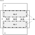
- FIG. 1B is a diagram illustrating the structure of an active layer of a thin film transistor not falling within the scope of the claims.
- the etch stop layer is not shown so that the structure of the active layer is revealed.
- the active layer AL includes a first semiconductor region AL-1, a second semiconductor region AL-2, and a plurality of semiconductor bridges AL-B each of which connecting the first semiconductor region Al-1 and the second semiconductor region AL-2.
- FIG. 1C is a diagram illustrating the structure of an active layer of a thin film transistor not falling within the scope of the claims.
- the first semiconductor region AL-1 includes a first non-overlapping portion NOL-1, a projection of which is outside that of the etch stop layer in plan view of the base substrate
- a second semiconductor region AL-2 includes a second non-overlapping portion NOL-2, a projection of which is outside that of the etch stop layer in plan view of the base substrate.
- FIG. 1C is a diagram illustrating the structure of an active layer of a thin film transistor not falling within the scope of the claims.
- the first semiconductor region AL-1 includes a first non-overlapping portion NOL-1, a projection of which is outside that of the etch stop layer in plan view of the base substrate
- a second semiconductor region AL-2 includes a second non-overlapping portion NOL-2, a projection of which is outside that of the etch stop layer in plan view of the base substrate.
- the first semiconductor region AL-1 further includes one or more first overlapping portion OL-1, a projection of which overlaps with that of the etch stop layer in plan view of the base substrate; and the second semiconductor region AL-2 further includes one or more second overlapping portion OL-2, a projection of which overlaps with that of the etch stop layer in plan view of the base substrate.
- the etch stop layer ESL is on a side of the active layer AL distal to the gate electrode G.
- Each etch stop block overlaps with corresponding semiconductor bridge AL-B (so that the semiconductor bridges AL-B is not shown in FIG. 1A ).
- the thin film transistor in FIGs. 1A-1C further includes a source electrode S in contact with and on a side of the first non-overlapping portion NOL-1 distal to the base substrate and a drain electrode D in contact with and on a side of the second non-overlapping portion NOL-2 distal to the base substrate.
- the active layer AL is an integral layer.
- the integral active layer in FIG. 1B includes a first semiconductor region AL-1 which is an integral semiconductor block connecting a plurality of first terminus of the plurality of semiconductor bridges AL-B, and a second semiconductor region AL-2 which is an integral semiconductor block connecting a plurality of second terminus of the plurality of semiconductor bridges AL-B.
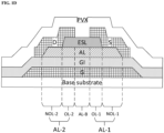
- FIG. ID is a cross-sectional view along line A-A' of the thin film transistor in FIG. 1A .
- FIG. 1E is a cross-sectional view along line B-B' of the thin film transistor in FIG. 1A .
- the thin film transistor includes a gate electrode G on a Base substrate, a gate insulating layer GI on a side of the gate electrode G distal to the Base substrate, an active layer AL on a side of the gate insulating layer GI distal to the gate electrode G, an etch stop layer ESL on a side of the active layer AL distal to the gate insulating layer GI, and a source electrode S and a drain electrode D on a side of the active layer AL distal to the gate insulating layer GI.
- the active layer AL partially overlaps with the etch stop layer ESL and partially overlaps with and is in contact with the source electrode S and the drain electrode D, in plan view of the base substrate.
- the active layer AL includes a first semiconductor region AL-1, a second semiconductor region AL-2, and a plurality of semiconductor bridges AL-B.
- the area where the active layer AL overlaps with the etch stop layer ESL includes an area corresponding to the plurality of the semiconductor bridges AL-B, a portion of the first semiconductor region (i.e., the first overlapping portion OL-1), and a portion of the second semiconductor region (i.e., the second overlapping portion OL-2).
- the area where the active layer overlaps with (and optionally in contact with) the source electrode is the first non-overlapping portion NOL-1
- the area where the active layer overlaps with (and optionally in contact with) the drain electrode is the second non-overlapping portion NOL-2.
- the first semiconductor region AL-1 is an integral semiconductor block connecting a plurality of first terminus of the plurality of semiconductor bridges AL-B
- the second semiconductor region AL-2 is an integral semiconductor block connecting a plurality of second terminus of the plurality of semiconductor bridges AL-B.
- the active layer AL include three semiconductor bridges AL-B, and the etch stop layer ESL includes three etch stop blocks, which corresponds to three semiconductor bridges AL-B in a one-to-one correspondence.
- FIG. 2A is a diagram illustrating the structure of a thin film transistor not falling within the scope of the claims.
- FIG. 2B is a diagram illustrating the structure of an active layer of a thin film transistor.
- the active layer in the embodiment include four semiconductor bridges AL-B, and the etch stop layer ESL includes four etch stop blocks, which corresponds to four semiconductor bridges AL-B in a one-to-one correspondence.
- FIG. 3A is a diagram illustrating the structure of a thin film transistor not falling within the scope of the claims.
- FIG. 3B is a diagram illustrating the structure of an active layer of a thin film transistor.
- the semiconductor bridge AL-B includes a middle portion having concaved-shaped lateral edges and a width narrower than widths of other portions of the semiconductor bridge AL-B.
- each etch stop block has a shape corresponding to that of the semiconductor bridge AL-B.
- the etch stop block includes a middle portion having concaved-shaped lateral edges and a width narrower than widths of other portions of the etch stop block.
- the semiconductor bridge AL-B includes a portion having an hourglass shape.
- the etch stop block includes a portion having an hourglass shape.
- FIG. 4A is a diagram illustrating the structure of a thin film transistor according to an embodiment of the claimed invention.
- FIG. 4B is a diagram illustrating the structure of an active layer of a thin film transistor in some embodiments.
- the source electrode S in the embodiment includes a source electrode main body S-M, a plurality of (e.g., two) source electrode teeth S-T integral with the source electrode main body and extending from the source electrode main body toward free ends of the plurality of source electrode teeth.
- the drain electrode D in the embodiment includes a drain electrode main body D-M, a plurality of (e.g., two) drain electrode teeth D-T integral with the drain electrode main body and extending from the drain electrode main body toward free ends of the plurality of drain electrode teeth.
- Each of the plurality of source electrode teeth and each of the plurality of drain electrode teeth are alternately arranged and spaced apart so that the source electrode and the drain electrode are interleaving.
- the active layer in the embodiment further includes a third semiconductor region AL-3, a fourth semiconductor region AL-4, and a plurality of additional semiconductor bridges AL-B each of which connecting the third semiconductor region AL-3 and the fourth semiconductor region AL-4.
- the plurality of additional semiconductor bridges AL-B are spaced apart from each other.
- the plurality of additional semiconductor bridges AL-B are substantially parallel to each other.
- FIG. 4C is a diagram illustrating the structure of an active layer of a thin film transistor in some embodiments.
- the first semiconductor region AL-1 in the embodiment includes a first non-overlapping portion NOL-1, a projection of which is outside that of the etch stop layer in plan view of the base substrate;
- the second semiconductor region AL-2 in the embodiment includes a second non-overlapping portion NOL-2, a projection of which is outside that of the etch stop layer in plan view of the base substrate;
- the third semiconductor region AL-3 in the embodiment includes a third non-overlapping portion NOL-3, a projection of which is outside that of the etch stop layer in plan view of the base substrate, and
- the fourth semiconductor region AL-4 in the embodiment includes a fourth non-overlapping portion NOL-4, a projection of which is outside that of the etch stop layer in plan view of the base substrate.
- the first semiconductor region AL-1 further includes one or more first overlapping portion OL-1, a projection of which overlaps with that of the etch stop layer in plan view of the base substrate;
- the second semiconductor region AL-2 further includes one or more second overlapping portion OL-2, a projection of which overlaps with that of the etch stop layer in plan view of the base substrate;
- the third semiconductor region AL-3 further includes one or more third overlapping portion OL-3, a projection of which overlaps with that of the etch stop layer in plan view of the base substrate, and the fourth semiconductor region AL-4 further includes one or more fourth overlapping portion OL-4, a projection of which overlaps with that of the etch stop layer in plan view of the base substrate.
- the source electrode S in the embodiment is in contact with and on a side of the first non-overlapping portion NOL-1 and the third non-overlapping portion NOL-3 distal to the base substrate
- the drain electrode D in the embodiment is in contact with and on a side of the second non-overlapping portion NOL-2 and the fourth non-overlapping portion NOL-4 distal to the base substrate.
- the first non-overlapping portion NOL-1 and the third non-overlapping portion NOL-3 are in contact with and on a side of the plurality of source electrode teeth proximal to the base substrate
- the second non-overlapping portion NOL-2 and the fourth non-overlapping portion NOL-4 are on a side of the plurality of drain electrode teeth proximal to the base substrate.
- FIG. 5A is a diagram illustrating the structure of a thin film transistor in some embodiments.
- FIG. 5B is a diagram illustrating the structure of an active layer of a thin film transistor in some embodiments.
- the source electrode S in the embodiment includes a source electrode main body S-M, two source electrode teeth S-T integral with the source electrode main body and extending from the source electrode main body toward free ends of the two source electrode teeth.
- the drain electrode D in the embodiment includes a drain electrode main body D-M, two drain electrode teeth D-T integral with the drain electrode main body and extending from the drain electrode main body toward free ends of the two drain electrode teeth. As shown in FIGs.
- the two source electrode teeth are sandwiched by the two drain electrode teeth so that one of the two drain electrode teeth is on one side of the source electrode S (e.g., the two source electrode teeth) and another of the two drain electrode teeth is on an opposite side of the source electrode S (e.g., the two source electrode teeth), and the source electrode S (e.g., the two source electrode teeth) are in the middle.
- the active layer in the embodiment further includes a third semiconductor region AL-3, a fourth semiconductor region AL-4, and a plurality of additional semiconductor bridges AL-B each of which connecting the third semiconductor region AL-3 and the fourth semiconductor region AL-4.
- the plurality of additional semiconductor bridges AL-B are spaced apart from each other.
- the plurality of additional semiconductor bridges AL-B are substantially parallel to each other.
- FIG. 5C is a diagram illustrating the structure of an active layer of a thin film transistor in some embodiments.
- the first semiconductor region AL-1 in the embodiment includes a first non-overlapping portion NOL-1, a projection of which is outside that of the etch stop layer in plan view of the base substrate;
- the second semiconductor region AL-2 in the embodiment includes a second non-overlapping portion NOL-2, a projection of which is outside that of the etch stop layer in plan view of the base substrate;
- the third semiconductor region AL-3 in the embodiment includes a third non-overlapping portion NOL-3, a projection of which is outside that of the etch stop layer in plan view of the base substrate, and
- the fourth semiconductor region AL-4 in the embodiment includes a fourth non-overlapping portion NOL-4, a projection of which is outside that of the etch stop layer in plan view of the base substrate.
- the first semiconductor region AL-1 further includes one or more first overlapping portion OL-1, a projection of which overlaps with that of the etch stop layer in plan view of the base substrate;
- the second semiconductor region AL-2 further includes one or more second overlapping portion OL-2, a projection of which overlaps with that of the etch stop layer in plan view of the base substrate;
- the third semiconductor region AL-3 further includes one or more third overlapping portion OL-3, a projection of which overlaps with that of the etch stop layer in plan view of the base substrate, and the fourth semiconductor region AL-4 further includes one or more fourth overlapping portion OL-4, a projection of which overlaps with that of the etch stop layer in plan view of the base substrate.
- the source electrode S in the embodiment is in contact with and on a side of the first non-overlapping portion NOL-1 and the third non-overlapping portion NOL-3 distal to the base substrate
- the drain electrode D in the embodiment is in contact with and on a side of the second non-overlapping portion NOL-2 and the fourth non-overlapping portion NOL-4 distal to the base substrate.
- the first non-overlapping portion NOL-1 and the third non-overlapping portion NOL-3 are in contact with and on a side of the plurality of source electrode teeth proximal to the base substrate
- the second non-overlapping portion NOL-2 and the fourth non-overlapping portion NOL-4 are on a side of the plurality of drain electrode teeth proximal to the base substrate.
- FIG. 6A is a diagram illustrating the structure of a thin film transistor in some embodiments.
- FIG. 6B is a diagram illustrating the structure of an active layer of a thin film transistor in some embodiments.
- the thin film transistor in FIGs. 6A-6B is largely similar to that of FIGs. 5A-5C except that the source electrode S in FIGs. 6A-6B is an integral source electrode block.
- the drain electrode D in the embodiment includes a drain electrode main body D-M, two drain electrode teeth D-T integral with the drain electrode main body and extending from the drain electrode main body toward free ends of the two drain electrode teeth.
- the integral source electrode block is sandwiched by the two drain electrode teeth so that one of the two drain electrode teeth is on one side of the integral source electrode block and another of the two drain electrode teeth is on an opposite side of the integral source electrode block, and the integral source electrode block is in the middle.
- the active layer in the embodiment further includes a third semiconductor region AL-3, a fourth semiconductor region AL-4, and a plurality of additional semiconductor bridges AL-B each of which connecting the third semiconductor region AL-3 and the fourth semiconductor region AL-4.
- the plurality of additional semiconductor bridges AL-B are spaced apart from each other.
- the plurality of additional semiconductor bridges AL-B are substantially parallel to each other.
- the source electrode S in the embodiment is in contact with and on a side of the first non-overlapping portion and the third non-overlapping portion distal to the base substrate
- the drain electrode D in the embodiment is in contact with and on a side of the second non-overlapping portion and the fourth non-overlapping portion distal to the base substrate.
- first non-overlapping portion and the third non-overlapping portion are in contact with and on a side of the integral source electrode block proximal to the base substrate, and the second non-overlapping portion and the fourth non-overlapping portion are in contact with and on a side of the two drain electrode teeth proximal to the base substrate.
- FIG. 7A is a diagram illustrating the structure of a thin film transistor in some embodiments.
- FIG. 7B is a diagram illustrating the structure of an active layer of a thin film transistor in some embodiments.
- the thin film transistor in the embodiment is largely similar to that of FIGs. 6A-6B , except that the first semiconductor region AL-1 and the third semiconductor region AL-3 in the embodiment form an integral semiconductor region AL-1/3.
- the first non-overlapping portion and the third non-overlapping portion in the embodiment constitute an integral non-overlapping portion.
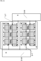
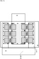
- FIG. 8 is a diagram illustrating the structure of a gate drive on array (GOA) circuit in some embodiments.
- the GOA circuit in the embodiment includes a thin film transistor described herein.
- the GOA circuit in the embodiment includes nine semiconductor bridges.
- the present thin film transistor is a thin film transistor in an organic light emitting display apparatus, e.g., a driving thin film transistor or an amplifying thin film transistor.
- Organic light emitting display apparatuses are current driven display apparatuses, placing a higher demand on thermal stability of the thin film transistor.
- the present thin film transistor has a much higher thermal stability as compared to the conventional thin film transistor, making them suitable for applications in organic light emitting display products.
- the present disclosure provides a method of fabricating a thin film transistor.
- the method includes forming an active layer on a base substrate having a first semiconductor region, a second semiconductor region, and a plurality of semiconductor bridges each of which connecting the first semiconductor region and the second semiconductor region; and forming an etch stop layer on a side of the active layer distal to the base substrate.
- the first semiconductor region and the second semiconductor region are formed to be spaced apart and arranged substantially along a first direction in a first plane.
- the plurality of semiconductor bridges are formed to be spaced apart from each other, each of which is arranged substantially along a second direction on a second plane.
- the first plane and the second plane are substantially parallel to each other.
- the first plane and the second plane are a same plane.
- the plurality of semiconductor bridges are formed to be substantially parallel to each other.
- the first direction is substantially perpendicular to the second direction.
- the active layer is made of a material comprising M1O a N b , wherein M1 is a single metal or a combination of metals, a > 0, and b ⁇ 0, e.g., the active layer is made of a metal oxide material or a metal oxynitride material.
- metal oxide active layer materials include, but are not limited to, indium gallium zinc oxide, zinc oxide, gallium oxide, indium oxide, HfInZnO (HIZO), amorphous InGaZnO (amorphous IGZO), InZnO, amorphous InZnO, ZnO:F, In 2 O 3 :Sn, In 2 O 3 :Mo, Cd 2 SnO 4 , ZnO:Al, TiO 2 :Nb, and Cd-Sn-O.
- HfInZnO HIZO
- amorphous InGaZnO amorphous IGZO
- InZnO amorphous InZnO
- ZnO:F In 2 O 3 :Sn
- In 2 O 3 :Mo Cd 2 SnO 4
- ZnO:Al TiO 2 :Nb
- Cd-Sn-O Cd-Sn-O.
- metal oxynitride active layer materials include, but are not limited to, zinc oxynitride, indium oxynitride, gallium oxynitride, tin oxynitride, cadmium oxynitride, aluminum oxynitride, germanium oxynitride, titanium oxynitride, silicon oxynitride, or combination thereof.
- the active layer is made of a material comprising M1O a N b doped with one or more metal element.
- the active layer is made of a material comprising M1O a N b doped with one or more non-metal element.
- the active layer is made of a material comprising M1O a N b doped with one or more metal element and one or more non-metal element.
- the etch stop layer is substantially resistant to an etchant for etching the first electrode and the second electrode (e.g., the source electrode and the drain electrode).
- the etch stop layer is substantially resistant to a wet etchant for etching the first electrode and the second electrode.
- the etch stop layer is made of a silicon-containing compound. Examples of silicon-containing compounds for making the etch stop layer include, but are not limited to, silicon oxide, silicon nitride, silicon oxynitride, silicon carbide, silicon oxycarbide, silicon, and silicon germanium.
- the first semiconductor region is formed to include a first non-overlapping portion, a projection of which is outside that of the etch stop layer in plan view of the base substrate.
- the second semiconductor region is formed to include a second non-overlapping portion, a projection of which is outside that of the etch stop layer in plan view of the base substrate.
- the method further includes forming a first electrode (e.g., a source electrode or a drain electrode) on a side of the first non-overlapping portion distal to the base substrate; and forming a second electrode (e.g., a drain electrode or a source electrode) on a side of the second non-overlapping portion distal to the base substrate.
- a first electrode e.g., a source electrode or a drain electrode
- a second electrode e.g., a drain electrode or a source electrode
- the first electrode e.g., a source electrode or a drain electrode
- the second electrode e.g., a drain electrode or a source electrode
- the second electrode is formed to be in contact with and on a side of the second non-overlapping portion distal to the base substrate.
- the method further includes forming an ohmic contact layer between the first electrode and the first non-overlapping portion. In some embodiments, the method further includes forming an ohmic contact layer between the second electrode and the second non-overlapping portion.
- the step of forming the active layer and the step of forming the etch stop layer are performed in a single patterning step.
- the single patterning step involves use of a half-tone mask plate or a gray-tone mask plate.
- the single patterning step includes forming a semiconductor material layer made of M1 O a N b , wherein M1 is a single metal or a combination of metals, a > 0, and b ⁇ 0, on the base substrate; forming an etch stop material layer on a side of the semiconductor material layer distal to the base substrate; coating a photoresist layer on a side of the etch stop material layer distal to the semiconductor material layer; exposing the photoresist layer with a half-tone mask plate or a gray-tone mask plate; developing the exposed photoresist layer to obtain a photoresist pattern comprising a first section corresponding to the active layer and a second section which is outside of the first section; the first section comprising a first zone corresponding
- the step of forming the active layer, the step of forming the first electrode, and the step of forming the second electrode are performed in a single patterning step.
- the method may include forming a semiconductor material layer including M1O a N b , wherein M1 is a single metal or a combination of metals, a > 0, and b ⁇ 0, on the base substrate; forming an etch stop material layer on a side of the semiconductor material layer distal to the base substrate; coating a first photoresist layer on a side of the etch stop material layer distal to the semiconductor material layer; exposing the first photoresist layer with a mask plate having a pattern corresponding to the etch stop layer; developing the exposed first photoresist layer to obtain a first photoresist pattern having a first section corresponding to the etch stop layer and a second section which is outside of the first section; removing the etch stop material layer in the second section thereby forming an etch stop layer pattern corresponding to the
- the semiconductor material layer may be formed by, e.g., coating, magnetron sputtering, and vapor deposition such as plasma enhanced chemical vapor deposition (PEVCD).
- PEVCD plasma enhanced chemical vapor deposition
- the etch stop material layer may be formed by, e.g., coating, magnetron sputtering, and vapor deposition such as plasma enhanced chemical vapor deposition (PEVCD).
- PEVCD plasma enhanced chemical vapor deposition
- the etch stop material layer may be removed by an etching process, e.g., a dry etching process.
- the semiconductor material layer may be removed by an etching process, e.g., a wet etching process.
- the photoresist layer may be removed by an ashing process.
- the electrode material layer may be removed by an etching process, e.g., a wet etching process.
- the thin film transistor is a bottom-gate thin film transistor.
- the method prior to forming the active layer, the method further comprises forming a gate electrode layer on the base substrate, and forming a gate insulating layer on a side of the gate electrode layer distal to the base substrate.
- the present disclosure provides a display panel having a thin film transistor described herein or fabricated by a method described herein.
- the present disclosure provides a display apparatus having a display panel described herein. Examples of appropriate display apparatuses include, but are not limited to, a liquid crystal display panel, an electronic paper, an organic light emitting display panel, a mobile phone, a tablet computer, a television, a monitor, a notebook computer, a digital album, a GPS, etc.
Landscapes
- Engineering & Computer Science (AREA)
- Physics & Mathematics (AREA)
- Geometry (AREA)
- Microelectronics & Electronic Packaging (AREA)
- Thin Film Transistor (AREA)
- Devices For Indicating Variable Information By Combining Individual Elements (AREA)
- Manufacturing & Machinery (AREA)
- Chemical & Material Sciences (AREA)
- Crystallography & Structural Chemistry (AREA)
- Liquid Crystal (AREA)
Claims (15)
- Dünnschichttransistor, aufweisend:ein Basissubstrat;eine aktive Schicht (AL) auf dem Basissubstrat, die einen ersten Halbleiterbereich (AL-1), einen zweiten Halbleiterbereich (AL-2) und mehrere Halbleiterbrücken (AL-B) aufweist, von denen jede den ersten Halbleiterbereich (AL-1) und den zweiten Halbleiterbereich (AL-2) verbindet; wobei die mehreren Halbleiterbrücken (AL-B) mit Abstand voneinander angeordnet sind; wobei die aktive Schicht (AL) aus einem Material hergestellt ist, das M1OaNb aufweist, wobei M1 ein einzelnes Metall oder eine Kombination von Metallen ist, mit a > 0 und b ≥ 0;eine Ätzstoppschicht (ESL) auf einer Seite der aktiven Schicht (AL) distal zu dem Basissubstrat; wobei der erste Halbleiterbereich (AL-1) einen ersten nicht überlappenden Abschnitt (NOL-1) aufweist, von dem eine Projektion sich außerhalb derjenigen der Ätzstoppschicht (ESL) in Draufsicht auf das Basissubstrat befindet; wobei der zweite Halbleiterbereich (AL-2) einen zweiten nicht überlappenden Abschnitt (NOL-2) aufweist, von dem eine Projektion sich außerhalb derjenigen der Ätzstoppschicht (ESL) in Draufsicht auf das Basissubstrat befindet;eine erste Elektrode auf einer Seite des ersten nicht überlappenden Abschnitts (NOL-1) distal zu dem Basissubstrat; undeine zweite Elektrode auf einer Seite des zweiten nicht überlappenden Abschnitts (NOL-2) distal zu dem Basissubstrat,dadurch gekennzeichnet, dass die aktive Schicht (AL) ferner einen dritten Halbleiterbereich (AL-3), einen vierten Halbleiterbereich (AL-4) und mehrere zusätzliche Halbleiterbrücken (AL-B) aufweist, von denen jede den dritten Halbleiterbereich (AL-3) und den vierten Halbleiterbereich (AL-4) verbindet; wobei die mehreren zusätzlichen Halbleiterbrücken (AL-B) mit Abstand voneinander angeordnet sind; der dritte Halbleiterbereich (AL-3) einen dritten nicht überlappenden Abschnitt (NOL-3) aufweist, dessen Projektion in Draufsicht auf das Basissubstrat sich außerhalb derjenigen der Ätzstoppschicht (ESL) befindet; der vierte Halbleiterbereich (AL-4) einen vierten nicht überlappenden Abschnitt (NOL-4) aufweist, dessen Projektion in Draufsicht auf das Basissubstrat sich außerhalb derjenigen der Ätzstoppschicht (ESL) befindet;die erste Elektrode sich auf einer Seite des dritten nicht überlappenden Abschnitts (NOL-3) distal zu dem Basissubstrat befindet; unddie zweite Elektrode sich auf einer Seite des vierten nicht überlappenden Abschnitts (NOL-4) distal zu dem Basissubstrat befindet.
- Dünnschichttransistor nach Anspruch 1, wobei der erste Halbleiterbereich (AL-1) ein einstückiger Halbleiterblock ist, der mehrere erste Enden der mehreren Halbleiterbrücken (AL-B) verbindet; der zweite Halbleiterbereich (AL-2) ein einstückiger Halbleiterblock ist, der mehrere zweite Enden der mehreren Halbleiterbrücken (AL-B) verbindet; der dritte Halbleiterbereich (AL-3) ein einstückiger Halbleiterblock ist, der mehrere erste Enden der mehreren zusätzlichen Halbleiterbrücken (AL-B) verbindet; der vierte Halbleiterbereich (AL-4) ein einstückiger Halbleiterblock ist, der mehrere zweite Enden der mehreren zusätzlichen Halbleiterbrücken (AL-B) verbindet.
- Dünnschichttransistor nach Anspruch 1, wobei die erste Elektrode mit dem ersten nicht überlappenden Abschnitt (NOL-1) in Kontakt ist und die zweite Elektrode mit dem zweiten nicht überlappenden Abschnitt (NOL-2) in Kontakt ist; die erste Elektrode mit dem dritten nicht überlappenden Abschnitt (NOL-3) in Kontakt ist und die zweite Elektrode mit dem vierten nicht überlappenden Abschnitt (NOL-4) in Kontakt ist.
- Dünnschichttransistor nach Anspruch 1, wobei die Ätzstoppschicht (ESL) mehrere Ätzstoppblöcke aufweist, die mit Abstand voneinander angeordnet sind, wobei jeder Ätzstoppblock mindestens teilweise mit der entsprechenden Halbleiterbrücke überlappt; und die Ätzstoppschicht (ESL) mehrere zusätzliche Ätzstoppblöcke aufweist, die mit Abstand voneinander angeordnet sind, wobei jeder zusätzliche Ätzstoppblock mindestens teilweise mit der entsprechenden zusätzlichen Halbleiterbrücke überlappt.
- Dünnschichttransistor nach Anspruch 1, wobei die mehreren Halbleiterbrücken (AL-B) mit einem Abstand im Bereich von etwa 3 µm bis etwa 15 µm voneinander angeordnet sind;jede der mehreren Halbleiterbrücken (AL-B) eine Breite im Bereich von etwa 3 µm bis etwa 20 µm aufweist;jede der mehreren Halbleiterbrücken (AL-B) eine rechteckige Form hat oder einen mittleren Abschnitt mit konkav gestalteten seitlichen Rändern und einer Breite aufweist, die schmaler ist als die Breiten der anderen Abschnitte jeder Halbleiterbrücke; unddie Ätzstoppschicht (ESL) gegen ein Ätzmittel zum Ätzen der ersten Elektrode und der zweiten Elektrode im Wesentlichen resistent ist.
- Dünnschichttransistor nach Anspruch 1, wobei die erste Elektrode einen ersten Elektrodenhauptkörper, mehrere erste Elektrodenzähne, die mit dem ersten Elektrodenhauptkörper einstückig sind und sich von dem ersten Elektrodenhauptkörper in Richtung von freien Enden der mehreren ersten Elektrodenzähne erstrecken, aufweist;die zweite Elektrode einen zweiten Elektrodenhauptkörper, mehrere zweite Elektrodenzähne, die einstückig mit dem zweiten Elektrodenhauptkörper gebildet sind und sich von dem zweiten Elektrodenhauptkörper in Richtung von freien Enden der mehreren zweiten Elektrodenzähnen erstrecken, aufweist;jeder der mehreren ersten Elektrodenzähne und jeder der mehreren zweiten Elektrodenzähne abwechselnd und mit Abstand voneinander angeordnet sind, so dass die erste Elektrode und die zweite Elektrode ineinander greifen;der erste nicht überlappende Abschnitt (NOL-1) und der dritte nicht überlappende Abschnitt (NOL-3) sich auf einer Seite der mehreren ersten Elektrodenzähne proximal zu dem Basissubstrat befinden, der zweite nicht überlappende Abschnitt (NOL-2) und der vierte nicht überlappende Abschnitt (NOL-4) sich auf einer Seite der mehreren zweiten Elektrodenzähne proximal zu dem Basissubstrat befinden.
- Dünnschichttransistor nach Anspruch 1, wobei die erste Elektrode einen ersten Elektrodenhauptkörper, zwei erste Elektrodenzähne, die mit dem ersten Elektrodenhauptkörper einstückig sind und sich von dem ersten Elektrodenhauptkörper in Richtung von freien Enden der beiden ersten Elektrodenzähne erstrecken, aufweist;die zweite Elektrode einen zweiten Elektrodenhauptkörper, zwei zweite Elektrodenzähne, die einstückig mit dem zweiten Elektrodenhauptkörper gebildet sind und sich von dem zweiten Elektrodenhauptkörper in Richtung von freien Enden der beiden zweiten Elektrodenzähne erstrecken, aufweist;die beiden ersten Elektrodenzähne von den beiden zweiten Elektrodenzähnen sandwichartig eingeschlossen sind, so dass sich einer der beiden zweiten Elektrodenzähne auf einer Seite der beiden ersten Elektrodenzähne und ein anderer der beiden zweiten Elektrodenzähne auf einer entgegengesetzten Seite der beiden ersten Elektrodenzähne befindet, und sich die beiden ersten Elektrodenzähne in der Mitte befinden;der erste nicht überlappende Abschnitt (NOL-1) und der dritte nicht überlappende Abschnitt (NOL-3) sich auf einer Seite der zwei ersten Elektrodenzähne proximal zu dem Basissubstrat befinden, der zweite nicht überlappende Abschnitt (NOL-2) und der vierte nicht überlappende Abschnitt (NOL-4) sich auf einer Seite der zwei zweiten Elektrodenzähne proximal zu dem Basissubstrat befinden.
- Dünnschichttransistor nach Anspruch 1, wobei die erste Elektrode einen einstückigen ersten Elektrodenblock aufweist;die zweite Elektrode einen zweiten Elektrodenhauptkörper und zwei zweite Elektrodenzähne aufweist, die einstückig mit dem zweiten Elektrodenhauptkörper gebildet sind und sich von dem zweiten Elektrodenhauptkörper in Richtung von freien Enden der beiden zweiten Elektrodenzähne erstrecken;der einstückige erste Elektrodenblock von den zwei zweiten Elektrodenzähnen eingeschlossen ist, so dass sich einer der zwei zweiten Elektrodenzähne auf einer Seite des einstückigen ersten Elektrodenblocks und der andere der zwei zweiten Elektrodenzähne sich auf einer entgegengesetzten Seite des einstückigen ersten Elektrodenblocks befindet, und sich der einstückige erste Elektrodenblock in der Mitte befindet;der erste nicht überlappende Abschnitt (NOL-1) und der dritte nicht überlappende Abschnitt (NOL-3) sich auf einer Seite des einstückigen ersten Elektrodenblocks proximal zu dem Basissubstrat befinden, der zweite nicht überlappende Abschnitt (NOL-2) und der vierte nicht überlappende Abschnitt (NOL-4) sich auf einer Seite der zwei zweiten Elektrodenzähne proximal zu dem Basissubstrat befinden.
- Dünnschichttransistor nach Anspruch 8, wobei der erste nicht überlappende Abschnitt (NOL-1) und der dritte nicht überlappende Abschnitt (NOL-3) einen einstückigen nicht überlappenden Abschnitt bilden.
- Dünnschichttransistor nach Anspruch 1, wobei der erste Halbleiterbereich (AL-1) ferner einen ersten überlappenden Abschnitt (OL-1) aufweist, dessen Projektion sich mit derjenigen der Ätzstoppschicht (ESL) in Draufsicht auf das Basissubstrat überlappt; der zweite Halbleiterbereich (AL-2) ferner einen zweiten überlappenden Abschnitt (OL-2) aufweist, dessen Projektion sich mit derjenigen der Ätzstoppschicht (ESL) in Draufsicht auf das Basissubstrat überlappt.
- Gate-Ansteuerung-auf-Array (GOA)-Schaltung, die einen Dünnschichttransistor nach einem der Ansprüche 1-10 aufweist.
- Anzeigetafel mit einem Dünnschichttransistor nach einem der Ansprüche 1-10.
- Verfahren zur Herstellung eines Dünnschichttransistors, umfassend:Bilden einer aktiven Schicht (AL) auf einem Basissubstrat mit einem ersten Halbleiterbereich (AL-1), einem zweiten Halbleiterbereich (AL-2) und mehreren Halbleiterbrücken (AL-B), von denen jede den ersten Halbleiterbereich (AL-1) und den zweiten Halbleiterbereich (AL-2) verbindet; wobei die mehreren Halbleiterbrücken (AL-B) mit Abstand voneinander angeordnet sind; wobei die aktive Schicht (AL) aus einem Material hergestellt ist, das M1OaNb aufweist, wobei M1 ein einzelnes Metall oder eine Kombination von Metallen ist, mit a > 0 und b ≥ 0;Bilden einer Ätzstoppschicht (ESL) auf einer Seite der aktiven Schicht (AL) distal zu dem Basissubstrat; wobei der erste Halbleiterbereich (AL-1) einen ersten nicht überlappenden Abschnitt (NOL-1) aufweist, von dem eine Projektion sich außerhalb derjenigen der Ätzstoppschicht (ESL) in Draufsicht auf das Basissubstrat befindet; wobei der zweite Halbleiterbereich (AL-2) einen zweiten nicht überlappenden Abschnitt (NOL-2) aufweist, von dem eine Projektion sich außerhalb derjenigen der Ätzstoppschicht (ESL) in Draufsicht auf das Basissubstrat befindet;Bilden einer ersten Elektrode auf einer Seite des ersten nicht überlappenden Abschnitts (NOL-1) distal zu dem Basissubstrat; undBilden einer zweiten Elektrode auf einer Seite des zweiten nicht überlappenden Abschnitts (NOL-2) distal zu dem Basissubstrat,dadurch gekennzeichnet, dass die aktive Schicht (AL) ferner einen dritten Halbleiterbereich (AL-3), einen vierten Halbleiterbereich (AL-4) und mehrere zusätzliche Halbleiterbrücken (AL-B) aufweist, von denen jede den dritten Halbleiterbereich (AL-3) und den vierten Halbleiterbereich (AL-4) verbindet; wobei die mehreren zusätzlichen Halbleiterbrücken (AL-B) mit Abstand voneinander angeordnet sind; der dritte Halbleiterbereich (AL-3) einen dritten nicht überlappenden Abschnitt (NOL-3) aufweist, dessen Projektion in Draufsicht auf das Basissubstrat sich außerhalb derjenigen der Ätzstoppschicht (ESL) befindet; der vierte Halbleiterbereich (AL-4) einen vierten nicht überlappenden Abschnitt (NOL-4) aufweist, dessen Projektion in Draufsicht auf das Basissubstrat sich außerhalb derjenigen der Ätzstoppschicht (ESL) befindet;die erste Elektrode sich auf einer Seite des dritten nicht überlappenden Abschnitts (NOL-3) distal zu dem Basissubstrat befindet; unddie zweite Elektrode sich auf einer Seite des vierten nicht überlappenden Abschnitts (NOL-4) distal zu dem Basissubstrat befindet.
- Verfahren nach Anspruch 13, wobei der Schritt des Bildens der aktiven Schicht (AL) und der Schritt des Bildens der Ätzstoppschicht (ESL) in einem einzelnen Strukturierungsschritt durchgeführt werden.
- Verfahren nach Anspruch 14, wobei der einzelne Strukturierungsschritt umfasst:Bilden einer Halbleitermaterialschicht mit M10aNb auf dem Basissubstrat, wobei M1 ein einzelnes Metall oder eine Kombination von Metallen ist, mit a > 0 und b ≥ 0,;Bilden einer Ätzstoppmaterialschicht auf einer Seite der Halbleitermaterialschicht distal zu dem Basissubstrat;Aufbringen einer Photoresistschicht auf einer Seite der Ätzstoppmaterialschicht distal zu der Halbleitermaterialschicht;Belichten der Photoresistschicht mit einer Halbtonmaskenplatte oder einer Grautonmaskenplatte;Entwickeln der belichteten Photoresistschicht, um ein Photoresistmuster zu erhalten, das einen ersten Abschnitt, der der aktiven Schicht (AL) entspricht, und einen zweiten Abschnitt, der sich außerhalb des ersten Abschnitts befindet, aufweist; wobei der erste Abschnitt eine erste Zone, die dem ersten nicht überlappenden Teil (NOL-1) und dem zweiten nicht überlappenden Teil (NOL-2) entspricht, und eine zweite Zone, die den verbleibenden Teilen des ersten Abschnitts entspricht, aufweist; wobei die Tiefe der zweiten Zone größer als diejenige der ersten Zone ist und das Photoresistmaterial in dem zweiten Abschnitt entfernt wird;Entfernen der Ätzstoppmaterialschicht in dem zweiten Abschnitt;Entfernen der Halbleitermaterialschicht in dem zweiten Abschnitt, so dass dadurch ein Muster der aktiven Schicht (AL) gebildet wird, das der aktiven Schicht (AL) entspricht;Entfernen der Photoresistschicht in der ersten Zone unter Beibehaltung der Photoresistschicht in der zweiten Zone;Entfernen der Ätzstoppmaterialschicht in der ersten Zone, so dass dadurch ein Ätzstoppschichtmuster gebildet wird, das der Ätzstoppschicht (ESL) entspricht; undEntfernen der Photoresistschicht in der zweiten Zone.
Applications Claiming Priority (1)
| Application Number | Priority Date | Filing Date | Title |
|---|---|---|---|
| PCT/CN2016/089409 WO2018006412A1 (en) | 2016-07-08 | 2016-07-08 | Thin film transistor, gate drive on array and display apparatus having the same, and fabricating method thereof |
Publications (3)
| Publication Number | Publication Date |
|---|---|
| EP3482420A1 EP3482420A1 (de) | 2019-05-15 |
| EP3482420A4 EP3482420A4 (de) | 2020-03-04 |
| EP3482420B1 true EP3482420B1 (de) | 2024-09-04 |
Family
ID=58215710
Family Applications (1)
| Application Number | Title | Priority Date | Filing Date |
|---|---|---|---|
| EP16880197.5A Active EP3482420B1 (de) | 2016-07-08 | 2016-07-08 | Dünnschichttransistor, gate-ansteuerung auf array und anzeigetafel damit sowie herstellungsverfahren dafür |
Country Status (8)
| Country | Link |
|---|---|
| US (1) | US10032917B1 (de) |
| EP (1) | EP3482420B1 (de) |
| JP (1) | JP6779884B2 (de) |
| KR (2) | KR102104471B1 (de) |
| CN (1) | CN106463545B (de) |
| BR (1) | BR112017023119B1 (de) |
| RU (1) | RU2705754C1 (de) |
| WO (1) | WO2018006412A1 (de) |
Families Citing this family (4)
| Publication number | Priority date | Publication date | Assignee | Title |
|---|---|---|---|---|
| CN109148303B (zh) * | 2018-07-23 | 2020-04-10 | 深圳市华星光电半导体显示技术有限公司 | 薄膜晶体管的制备方法 |
| CN109360858A (zh) * | 2018-09-28 | 2019-02-19 | 合肥鑫晟光电科技有限公司 | 薄膜晶体管、显示基板及修复方法、显示装置 |
| CN111430368B (zh) * | 2020-03-30 | 2023-01-20 | 友达光电(苏州)有限公司 | 显示装置 |
| KR20240086302A (ko) | 2022-12-09 | 2024-06-18 | 엘지디스플레이 주식회사 | 박막 트랜지스터 및 이를 포함하는 표시장치 |
Family Cites Families (28)
| Publication number | Priority date | Publication date | Assignee | Title |
|---|---|---|---|---|
| JP3520713B2 (ja) * | 1997-03-26 | 2004-04-19 | セイコーエプソン株式会社 | 薄膜トランジスタ及びそれを用いた液晶表示装置及び薄膜トランジスタ回路 |
| JP2003332578A (ja) | 2002-05-09 | 2003-11-21 | Sharp Corp | 薄膜トランジスタ及びその製造方法並びにこれを用いた液晶表示装置 |
| KR100553935B1 (ko) * | 2003-08-20 | 2006-02-24 | 엘지.필립스 엘시디 주식회사 | 액정표시장치 및 그 제조방법 |
| TWI255150B (en) * | 2003-12-22 | 2006-05-11 | Lg Philips Lcd Co Ltd | Organic electroluminescent device and method of fabricating the same |
| KR100632214B1 (ko) * | 2003-12-22 | 2006-10-09 | 엘지.필립스 엘시디 주식회사 | 유기전계 발광소자와 그 제조방법 |
| KR100603832B1 (ko) * | 2004-05-03 | 2006-07-24 | 엘지.필립스 엘시디 주식회사 | 열분산형 멀티채널 트랜지스터와 그 제조방법 |
| KR101107712B1 (ko) * | 2005-02-28 | 2012-01-25 | 엘지디스플레이 주식회사 | 액정표시장치 |
| JP2007005395A (ja) * | 2005-06-21 | 2007-01-11 | Mitsubishi Electric Corp | 薄膜トランジスタ |
| JP2007157916A (ja) | 2005-12-02 | 2007-06-21 | Idemitsu Kosan Co Ltd | Tft基板及びtft基板の製造方法 |
| JP2008310298A (ja) * | 2007-05-16 | 2008-12-25 | Advanced Lcd Technologies Development Center Co Ltd | 表示装置および電子装置 |
| EP2001047A1 (de) * | 2007-06-07 | 2008-12-10 | Semiconductor Energy Laboratory Co, Ltd. | Halbleiterbauelement |
| JP2009060001A (ja) * | 2007-09-03 | 2009-03-19 | Casio Comput Co Ltd | フォトトランジスタ |
| KR101501699B1 (ko) * | 2007-09-19 | 2015-03-16 | 삼성디스플레이 주식회사 | 유기 박막 트랜지스터 기판 및 이의 제조 방법 |
| JP2008085357A (ja) | 2007-11-06 | 2008-04-10 | Nec Corp | 電界効果型トランジスタの製造方法 |
| KR101463028B1 (ko) * | 2008-06-30 | 2014-11-19 | 엘지디스플레이 주식회사 | 산화물 박막 트랜지스터의 제조방법 |
| TWI424506B (zh) * | 2008-08-08 | 2014-01-21 | 半導體能源研究所股份有限公司 | 半導體裝置的製造方法 |
| CN102356352A (zh) * | 2009-03-24 | 2012-02-15 | 夏普株式会社 | Tft基板和使用该tft基板的液晶显示装置 |
| US9029861B2 (en) * | 2010-07-16 | 2015-05-12 | Sharp Kabushiki Kaisha | Thin film transistor and shift register |
| TWI555205B (zh) | 2010-11-05 | 2016-10-21 | 半導體能源研究所股份有限公司 | 半導體裝置及半導體裝置的製造方法 |
| KR20130050712A (ko) * | 2011-11-08 | 2013-05-16 | 삼성디스플레이 주식회사 | 박막 트랜지스터 어레이 기판, 이를 포함하는 유기 발광 표시 장치 및 그 제조 방법 |
| JP2013161895A (ja) * | 2012-02-03 | 2013-08-19 | Sony Corp | 薄膜トランジスタ、表示装置および電子機器 |
| CN102723334B (zh) * | 2012-06-07 | 2015-04-08 | 南京中电熊猫液晶显示科技有限公司 | 一种金属氧化物薄膜晶体基板及其制造方法和液晶显示器 |
| TWI611566B (zh) * | 2013-02-25 | 2018-01-11 | Semiconductor Energy Laboratory Co., Ltd. | 顯示裝置和電子裝置 |
| JP6490914B2 (ja) * | 2013-06-28 | 2019-03-27 | 株式会社半導体エネルギー研究所 | 半導体装置の作製方法 |
| CN103941448B (zh) * | 2013-12-26 | 2018-03-02 | 上海天马微电子有限公司 | 一种薄膜晶体管阵列基板及其制备方法、液晶显示器 |
| KR102230301B1 (ko) * | 2014-01-06 | 2021-03-22 | 삼성디스플레이 주식회사 | 박막 트랜지스터 및 그 제조 방법 |
| EP2960943B1 (de) * | 2014-06-27 | 2019-08-07 | LG Display Co., Ltd. | Dünnfilmtransistor für eine anzeigevorrichtung |
| CN104914639A (zh) | 2015-06-26 | 2015-09-16 | 深圳市华星光电技术有限公司 | 一种tft基板及显示装置 |
-
2016
- 2016-07-08 US US15/543,673 patent/US10032917B1/en active Active
- 2016-07-08 WO PCT/CN2016/089409 patent/WO2018006412A1/en not_active Ceased
- 2016-07-08 BR BR112017023119-0A patent/BR112017023119B1/pt active IP Right Grant
- 2016-07-08 CN CN201680000573.1A patent/CN106463545B/zh active Active
- 2016-07-08 KR KR1020197018645A patent/KR102104471B1/ko active Active
- 2016-07-08 KR KR1020177020017A patent/KR20180016330A/ko not_active Ceased
- 2016-07-08 EP EP16880197.5A patent/EP3482420B1/de active Active
- 2016-07-08 RU RU2017131645A patent/RU2705754C1/ru active
- 2016-07-08 JP JP2017538210A patent/JP6779884B2/ja active Active
Also Published As
| Publication number | Publication date |
|---|---|
| RU2705754C1 (ru) | 2019-11-11 |
| KR102104471B1 (ko) | 2020-04-24 |
| US10032917B1 (en) | 2018-07-24 |
| EP3482420A4 (de) | 2020-03-04 |
| US20180212050A1 (en) | 2018-07-26 |
| WO2018006412A1 (en) | 2018-01-11 |
| JP6779884B2 (ja) | 2020-11-04 |
| EP3482420A1 (de) | 2019-05-15 |
| KR20190079708A (ko) | 2019-07-05 |
| CN106463545B (zh) | 2019-11-01 |
| BR112017023119B1 (pt) | 2022-11-16 |
| KR20180016330A (ko) | 2018-02-14 |
| CN106463545A (zh) | 2017-02-22 |
| JP2019520691A (ja) | 2019-07-18 |
| BR112017023119A2 (en) | 2018-07-10 |
Similar Documents
| Publication | Publication Date | Title |
|---|---|---|
| JP6483843B2 (ja) | アレイ基板及びその製造方法、表示装置 | |
| KR101579135B1 (ko) | 박막 트랜지스터 기판 및 그 제조 방법 | |
| CN100378902C (zh) | 薄膜晶体管阵列板及其制造方法 | |
| CN108062915B (zh) | 阵列基板及其制造方法、触控显示面板、触控显示装置 | |
| CN104851888B (zh) | 薄膜晶体管阵列面板 | |
| CN104835851B (zh) | 一种薄膜晶体管、阵列基板及显示装置 | |
| KR102080484B1 (ko) | 액정표시장치용 어레이기판 및 그의 제조방법 | |
| US10032917B1 (en) | Thin film transistor, gate drive on array and display apparatus having the same, and fabricating method thereof | |
| WO2017118112A1 (zh) | 阵列基板和显示装置 | |
| WO2017177734A1 (zh) | 阵列基板、制造方法以及显示面板和电子装置 | |
| US11143920B2 (en) | Display panel | |
| US20200258919A1 (en) | Thin film transistor, array substrate, display apparatus, and method of fabricating thin film transistor | |
| US20090224247A1 (en) | Liquid crystal display device | |
| JP2021015954A5 (de) | ||
| JP7042621B2 (ja) | アレイ基板、表示パネル、アレイ基板を備える表示装置及びアレイ基板の製造方法 | |
| US9178024B2 (en) | Thin film transistor display panel and manufacturing method thereof | |
| TWI483401B (zh) | 薄膜電晶體與顯示面板 | |
| CN110993617A (zh) | 阵列基板、显示面板及显示装置 | |
| US8431929B2 (en) | Semiconductor structures | |
| TWI401750B (zh) | 薄膜電晶體及其製造方法 | |
| CN106856199A (zh) | 显示面板及其制造方法 | |
| TW202132955A (zh) | 觸控面板 | |
| KR20050017900A (ko) | 박막 트랜지스터 표시판 및 그 제조 방법 | |
| CN104777640A (zh) | 液晶显示器及其制造方法 | |
| JP2010040582A (ja) | 有機電界効果トランジスタ |
Legal Events
| Date | Code | Title | Description |
|---|---|---|---|
| STAA | Information on the status of an ep patent application or granted ep patent |
Free format text: STATUS: UNKNOWN |
|
| STAA | Information on the status of an ep patent application or granted ep patent |
Free format text: STATUS: THE INTERNATIONAL PUBLICATION HAS BEEN MADE |
|
| PUAI | Public reference made under article 153(3) epc to a published international application that has entered the european phase |
Free format text: ORIGINAL CODE: 0009012 |
|
| STAA | Information on the status of an ep patent application or granted ep patent |
Free format text: STATUS: REQUEST FOR EXAMINATION WAS MADE |
|
| 17P | Request for examination filed |
Effective date: 20170707 |
|
| AK | Designated contracting states |
Kind code of ref document: A1 Designated state(s): AL AT BE BG CH CY CZ DE DK EE ES FI FR GB GR HR HU IE IS IT LI LT LU LV MC MK MT NL NO PL PT RO RS SE SI SK SM TR |
|
| AX | Request for extension of the european patent |
Extension state: BA ME |
|
| DAV | Request for validation of the european patent (deleted) | ||
| DAX | Request for extension of the european patent (deleted) | ||
| A4 | Supplementary search report drawn up and despatched |
Effective date: 20200205 |
|
| RIC1 | Information provided on ipc code assigned before grant |
Ipc: H01L 29/786 20060101AFI20200130BHEP Ipc: H01L 21/34 20060101ALI20200130BHEP Ipc: H01L 27/12 20060101ALI20200130BHEP Ipc: H01L 21/02 20060101ALI20200130BHEP |
|
| STAA | Information on the status of an ep patent application or granted ep patent |
Free format text: STATUS: EXAMINATION IS IN PROGRESS |
|
| 17Q | First examination report despatched |
Effective date: 20220202 |
|
| GRAP | Despatch of communication of intention to grant a patent |
Free format text: ORIGINAL CODE: EPIDOSNIGR1 |
|
| STAA | Information on the status of an ep patent application or granted ep patent |
Free format text: STATUS: GRANT OF PATENT IS INTENDED |
|
| INTG | Intention to grant announced |
Effective date: 20240528 |
|
| GRAS | Grant fee paid |
Free format text: ORIGINAL CODE: EPIDOSNIGR3 |
|
| GRAA | (expected) grant |
Free format text: ORIGINAL CODE: 0009210 |
|
| STAA | Information on the status of an ep patent application or granted ep patent |
Free format text: STATUS: THE PATENT HAS BEEN GRANTED |
|
| AK | Designated contracting states |
Kind code of ref document: B1 Designated state(s): AL AT BE BG CH CY CZ DE DK EE ES FI FR GB GR HR HU IE IS IT LI LT LU LV MC MK MT NL NO PL PT RO RS SE SI SK SM TR |
|
| REG | Reference to a national code |
Ref country code: GB Ref legal event code: FG4D |
|
| REG | Reference to a national code |
Ref country code: CH Ref legal event code: EP |
|
| REG | Reference to a national code |
Ref country code: IE Ref legal event code: FG4D |
|
| REG | Reference to a national code |
Ref country code: DE Ref legal event code: R096 Ref document number: 602016089299 Country of ref document: DE |
|
| REG | Reference to a national code |
Ref country code: DE Ref legal event code: R079 Ref document number: 602016089299 Country of ref document: DE Free format text: PREVIOUS MAIN CLASS: H01L0029786000 Ipc: H10D0030670000 |
|
| REG | Reference to a national code |
Ref country code: LT Ref legal event code: MG9D |
|
| REG | Reference to a national code |
Ref country code: NL Ref legal event code: MP Effective date: 20240904 |
|
| PG25 | Lapsed in a contracting state [announced via postgrant information from national office to epo] |
Ref country code: NO Free format text: LAPSE BECAUSE OF FAILURE TO SUBMIT A TRANSLATION OF THE DESCRIPTION OR TO PAY THE FEE WITHIN THE PRESCRIBED TIME-LIMIT Effective date: 20241204 |
|
| PG25 | Lapsed in a contracting state [announced via postgrant information from national office to epo] |
Ref country code: PL Free format text: LAPSE BECAUSE OF FAILURE TO SUBMIT A TRANSLATION OF THE DESCRIPTION OR TO PAY THE FEE WITHIN THE PRESCRIBED TIME-LIMIT Effective date: 20240904 Ref country code: GR Free format text: LAPSE BECAUSE OF FAILURE TO SUBMIT A TRANSLATION OF THE DESCRIPTION OR TO PAY THE FEE WITHIN THE PRESCRIBED TIME-LIMIT Effective date: 20241205 Ref country code: FI Free format text: LAPSE BECAUSE OF FAILURE TO SUBMIT A TRANSLATION OF THE DESCRIPTION OR TO PAY THE FEE WITHIN THE PRESCRIBED TIME-LIMIT Effective date: 20240904 |
|
| PG25 | Lapsed in a contracting state [announced via postgrant information from national office to epo] |
Ref country code: BG Free format text: LAPSE BECAUSE OF FAILURE TO SUBMIT A TRANSLATION OF THE DESCRIPTION OR TO PAY THE FEE WITHIN THE PRESCRIBED TIME-LIMIT Effective date: 20240904 |
|
| PG25 | Lapsed in a contracting state [announced via postgrant information from national office to epo] |
Ref country code: LV Free format text: LAPSE BECAUSE OF FAILURE TO SUBMIT A TRANSLATION OF THE DESCRIPTION OR TO PAY THE FEE WITHIN THE PRESCRIBED TIME-LIMIT Effective date: 20240904 |
|
| PG25 | Lapsed in a contracting state [announced via postgrant information from national office to epo] |
Ref country code: HR Free format text: LAPSE BECAUSE OF FAILURE TO SUBMIT A TRANSLATION OF THE DESCRIPTION OR TO PAY THE FEE WITHIN THE PRESCRIBED TIME-LIMIT Effective date: 20240904 |
|
| PG25 | Lapsed in a contracting state [announced via postgrant information from national office to epo] |
Ref country code: ES Free format text: LAPSE BECAUSE OF FAILURE TO SUBMIT A TRANSLATION OF THE DESCRIPTION OR TO PAY THE FEE WITHIN THE PRESCRIBED TIME-LIMIT Effective date: 20240904 Ref country code: RS Free format text: LAPSE BECAUSE OF FAILURE TO SUBMIT A TRANSLATION OF THE DESCRIPTION OR TO PAY THE FEE WITHIN THE PRESCRIBED TIME-LIMIT Effective date: 20241204 |
|
| PG25 | Lapsed in a contracting state [announced via postgrant information from national office to epo] |
Ref country code: RS Free format text: LAPSE BECAUSE OF FAILURE TO SUBMIT A TRANSLATION OF THE DESCRIPTION OR TO PAY THE FEE WITHIN THE PRESCRIBED TIME-LIMIT Effective date: 20241204 Ref country code: PL Free format text: LAPSE BECAUSE OF FAILURE TO SUBMIT A TRANSLATION OF THE DESCRIPTION OR TO PAY THE FEE WITHIN THE PRESCRIBED TIME-LIMIT Effective date: 20240904 Ref country code: NO Free format text: LAPSE BECAUSE OF FAILURE TO SUBMIT A TRANSLATION OF THE DESCRIPTION OR TO PAY THE FEE WITHIN THE PRESCRIBED TIME-LIMIT Effective date: 20241204 Ref country code: LV Free format text: LAPSE BECAUSE OF FAILURE TO SUBMIT A TRANSLATION OF THE DESCRIPTION OR TO PAY THE FEE WITHIN THE PRESCRIBED TIME-LIMIT Effective date: 20240904 Ref country code: HR Free format text: LAPSE BECAUSE OF FAILURE TO SUBMIT A TRANSLATION OF THE DESCRIPTION OR TO PAY THE FEE WITHIN THE PRESCRIBED TIME-LIMIT Effective date: 20240904 Ref country code: GR Free format text: LAPSE BECAUSE OF FAILURE TO SUBMIT A TRANSLATION OF THE DESCRIPTION OR TO PAY THE FEE WITHIN THE PRESCRIBED TIME-LIMIT Effective date: 20241205 Ref country code: FI Free format text: LAPSE BECAUSE OF FAILURE TO SUBMIT A TRANSLATION OF THE DESCRIPTION OR TO PAY THE FEE WITHIN THE PRESCRIBED TIME-LIMIT Effective date: 20240904 Ref country code: ES Free format text: LAPSE BECAUSE OF FAILURE TO SUBMIT A TRANSLATION OF THE DESCRIPTION OR TO PAY THE FEE WITHIN THE PRESCRIBED TIME-LIMIT Effective date: 20240904 Ref country code: BG Free format text: LAPSE BECAUSE OF FAILURE TO SUBMIT A TRANSLATION OF THE DESCRIPTION OR TO PAY THE FEE WITHIN THE PRESCRIBED TIME-LIMIT Effective date: 20240904 |
|
| REG | Reference to a national code |
Ref country code: AT Ref legal event code: MK05 Ref document number: 1721351 Country of ref document: AT Kind code of ref document: T Effective date: 20240904 |
|
| PG25 | Lapsed in a contracting state [announced via postgrant information from national office to epo] |
Ref country code: NL Free format text: LAPSE BECAUSE OF FAILURE TO SUBMIT A TRANSLATION OF THE DESCRIPTION OR TO PAY THE FEE WITHIN THE PRESCRIBED TIME-LIMIT Effective date: 20240904 |
|
| PG25 | Lapsed in a contracting state [announced via postgrant information from national office to epo] |
Ref country code: IS Free format text: LAPSE BECAUSE OF FAILURE TO SUBMIT A TRANSLATION OF THE DESCRIPTION OR TO PAY THE FEE WITHIN THE PRESCRIBED TIME-LIMIT Effective date: 20250104 Ref country code: PT Free format text: LAPSE BECAUSE OF FAILURE TO SUBMIT A TRANSLATION OF THE DESCRIPTION OR TO PAY THE FEE WITHIN THE PRESCRIBED TIME-LIMIT Effective date: 20250106 |
|
| PG25 | Lapsed in a contracting state [announced via postgrant information from national office to epo] |
Ref country code: RO Free format text: LAPSE BECAUSE OF FAILURE TO SUBMIT A TRANSLATION OF THE DESCRIPTION OR TO PAY THE FEE WITHIN THE PRESCRIBED TIME-LIMIT Effective date: 20240904 Ref country code: SM Free format text: LAPSE BECAUSE OF FAILURE TO SUBMIT A TRANSLATION OF THE DESCRIPTION OR TO PAY THE FEE WITHIN THE PRESCRIBED TIME-LIMIT Effective date: 20240904 |
|
| PG25 | Lapsed in a contracting state [announced via postgrant information from national office to epo] |
Ref country code: EE Free format text: LAPSE BECAUSE OF FAILURE TO SUBMIT A TRANSLATION OF THE DESCRIPTION OR TO PAY THE FEE WITHIN THE PRESCRIBED TIME-LIMIT Effective date: 20240904 Ref country code: AT Free format text: LAPSE BECAUSE OF FAILURE TO SUBMIT A TRANSLATION OF THE DESCRIPTION OR TO PAY THE FEE WITHIN THE PRESCRIBED TIME-LIMIT Effective date: 20240904 |
|
| PG25 | Lapsed in a contracting state [announced via postgrant information from national office to epo] |
Ref country code: CZ Free format text: LAPSE BECAUSE OF FAILURE TO SUBMIT A TRANSLATION OF THE DESCRIPTION OR TO PAY THE FEE WITHIN THE PRESCRIBED TIME-LIMIT Effective date: 20240904 |
|
| PG25 | Lapsed in a contracting state [announced via postgrant information from national office to epo] |
Ref country code: IT Free format text: LAPSE BECAUSE OF FAILURE TO SUBMIT A TRANSLATION OF THE DESCRIPTION OR TO PAY THE FEE WITHIN THE PRESCRIBED TIME-LIMIT Effective date: 20240904 Ref country code: SK Free format text: LAPSE BECAUSE OF FAILURE TO SUBMIT A TRANSLATION OF THE DESCRIPTION OR TO PAY THE FEE WITHIN THE PRESCRIBED TIME-LIMIT Effective date: 20240904 |
|
| REG | Reference to a national code |
Ref country code: DE Ref legal event code: R097 Ref document number: 602016089299 Country of ref document: DE |
|
| PG25 | Lapsed in a contracting state [announced via postgrant information from national office to epo] |
Ref country code: DK Free format text: LAPSE BECAUSE OF FAILURE TO SUBMIT A TRANSLATION OF THE DESCRIPTION OR TO PAY THE FEE WITHIN THE PRESCRIBED TIME-LIMIT Effective date: 20240904 |
|
| PLBE | No opposition filed within time limit |
Free format text: ORIGINAL CODE: 0009261 |
|
| STAA | Information on the status of an ep patent application or granted ep patent |
Free format text: STATUS: NO OPPOSITION FILED WITHIN TIME LIMIT |
|
| 26N | No opposition filed |
Effective date: 20250605 |
|
| PG25 | Lapsed in a contracting state [announced via postgrant information from national office to epo] |
Ref country code: SE Free format text: LAPSE BECAUSE OF FAILURE TO SUBMIT A TRANSLATION OF THE DESCRIPTION OR TO PAY THE FEE WITHIN THE PRESCRIBED TIME-LIMIT Effective date: 20240904 |
|
| PGFP | Annual fee paid to national office [announced via postgrant information from national office to epo] |
Ref country code: DE Payment date: 20250722 Year of fee payment: 10 |
|
| REG | Reference to a national code |
Ref country code: CH Ref legal event code: H13 Free format text: ST27 STATUS EVENT CODE: U-0-0-H10-H13 (AS PROVIDED BY THE NATIONAL OFFICE) Effective date: 20260224 |
|
| PG25 | Lapsed in a contracting state [announced via postgrant information from national office to epo] |
Ref country code: LU Free format text: LAPSE BECAUSE OF NON-PAYMENT OF DUE FEES Effective date: 20250708 |
|
| GBPC | Gb: european patent ceased through non-payment of renewal fee |
Effective date: 20250708 |
|
| REG | Reference to a national code |
Ref country code: BE Ref legal event code: MM Effective date: 20250731 |
|
| PG25 | Lapsed in a contracting state [announced via postgrant information from national office to epo] |
Ref country code: GB Free format text: LAPSE BECAUSE OF NON-PAYMENT OF DUE FEES Effective date: 20250708 |
|
| PG25 | Lapsed in a contracting state [announced via postgrant information from national office to epo] |
Ref country code: BE Free format text: LAPSE BECAUSE OF NON-PAYMENT OF DUE FEES Effective date: 20250731 |
|
| PG25 | Lapsed in a contracting state [announced via postgrant information from national office to epo] |
Ref country code: FR Free format text: LAPSE BECAUSE OF NON-PAYMENT OF DUE FEES Effective date: 20250731 |
|
| PG25 | Lapsed in a contracting state [announced via postgrant information from national office to epo] |
Ref country code: CH Free format text: LAPSE BECAUSE OF NON-PAYMENT OF DUE FEES Effective date: 20250731 |