EP2960943B1 - Dünnfilmtransistor für eine anzeigevorrichtung - Google Patents
Dünnfilmtransistor für eine anzeigevorrichtung Download PDFInfo
- Publication number
- EP2960943B1 EP2960943B1 EP15173323.5A EP15173323A EP2960943B1 EP 2960943 B1 EP2960943 B1 EP 2960943B1 EP 15173323 A EP15173323 A EP 15173323A EP 2960943 B1 EP2960943 B1 EP 2960943B1
- Authority
- EP
- European Patent Office
- Prior art keywords
- gate electrode
- active layer
- tft
- disposed
- lines
- Prior art date
- Legal status (The legal status is an assumption and is not a legal conclusion. Google has not performed a legal analysis and makes no representation as to the accuracy of the status listed.)
- Active
Links
- 239000010409 thin film Substances 0.000 title claims description 7
- 239000012212 insulator Substances 0.000 claims description 34
- 239000000758 substrate Substances 0.000 claims description 10
- 238000010586 diagram Methods 0.000 description 54
- 230000003071 parasitic effect Effects 0.000 description 51
- 230000007547 defect Effects 0.000 description 18
- 229910021417 amorphous silicon Inorganic materials 0.000 description 14
- 229910021420 polycrystalline silicon Inorganic materials 0.000 description 14
- 238000013461 design Methods 0.000 description 12
- 238000005259 measurement Methods 0.000 description 12
- 238000004519 manufacturing process Methods 0.000 description 11
- 230000000694 effects Effects 0.000 description 8
- 230000005684 electric field Effects 0.000 description 8
- 229920005591 polysilicon Polymers 0.000 description 7
- 230000008901 benefit Effects 0.000 description 6
- 239000011368 organic material Substances 0.000 description 6
- 238000000034 method Methods 0.000 description 5
- 230000002708 enhancing effect Effects 0.000 description 4
- AMGQUBHHOARCQH-UHFFFAOYSA-N indium;oxotin Chemical compound [In].[Sn]=O AMGQUBHHOARCQH-UHFFFAOYSA-N 0.000 description 4
- 239000000463 material Substances 0.000 description 4
- 238000000059 patterning Methods 0.000 description 4
- 230000008569 process Effects 0.000 description 4
- 239000012780 transparent material Substances 0.000 description 4
- 239000003990 capacitor Substances 0.000 description 3
- 229910052751 metal Inorganic materials 0.000 description 2
- 239000002184 metal Substances 0.000 description 2
- 238000012986 modification Methods 0.000 description 2
- 230000004048 modification Effects 0.000 description 2
- 230000004044 response Effects 0.000 description 2
- 239000003086 colorant Substances 0.000 description 1
- 230000007423 decrease Effects 0.000 description 1
- 230000001419 dependent effect Effects 0.000 description 1
- 230000005281 excited state Effects 0.000 description 1
- 230000006870 function Effects 0.000 description 1
- 230000005283 ground state Effects 0.000 description 1
- 239000011159 matrix material Substances 0.000 description 1
- 230000002123 temporal effect Effects 0.000 description 1
- 238000012546 transfer Methods 0.000 description 1
Images


Classifications
-
- H—ELECTRICITY
- H01—ELECTRIC ELEMENTS
- H01L—SEMICONDUCTOR DEVICES NOT COVERED BY CLASS H10
- H01L29/00—Semiconductor devices specially adapted for rectifying, amplifying, oscillating or switching and having potential barriers; Capacitors or resistors having potential barriers, e.g. a PN-junction depletion layer or carrier concentration layer; Details of semiconductor bodies or of electrodes thereof ; Multistep manufacturing processes therefor
- H01L29/66—Types of semiconductor device ; Multistep manufacturing processes therefor
- H01L29/68—Types of semiconductor device ; Multistep manufacturing processes therefor controllable by only the electric current supplied, or only the electric potential applied, to an electrode which does not carry the current to be rectified, amplified or switched
- H01L29/76—Unipolar devices, e.g. field effect transistors
- H01L29/772—Field effect transistors
- H01L29/78—Field effect transistors with field effect produced by an insulated gate
- H01L29/786—Thin film transistors, i.e. transistors with a channel being at least partly a thin film
- H01L29/78696—Thin film transistors, i.e. transistors with a channel being at least partly a thin film characterised by the structure of the channel, e.g. multichannel, transverse or longitudinal shape, length or width, doping structure, or the overlap or alignment between the channel and the gate, the source or the drain, or the contacting structure of the channel
-
- H—ELECTRICITY
- H01—ELECTRIC ELEMENTS
- H01L—SEMICONDUCTOR DEVICES NOT COVERED BY CLASS H10
- H01L27/00—Devices consisting of a plurality of semiconductor or other solid-state components formed in or on a common substrate
- H01L27/02—Devices consisting of a plurality of semiconductor or other solid-state components formed in or on a common substrate including semiconductor components specially adapted for rectifying, oscillating, amplifying or switching and having potential barriers; including integrated passive circuit elements having potential barriers
- H01L27/12—Devices consisting of a plurality of semiconductor or other solid-state components formed in or on a common substrate including semiconductor components specially adapted for rectifying, oscillating, amplifying or switching and having potential barriers; including integrated passive circuit elements having potential barriers the substrate being other than a semiconductor body, e.g. an insulating body
- H01L27/1214—Devices consisting of a plurality of semiconductor or other solid-state components formed in or on a common substrate including semiconductor components specially adapted for rectifying, oscillating, amplifying or switching and having potential barriers; including integrated passive circuit elements having potential barriers the substrate being other than a semiconductor body, e.g. an insulating body comprising a plurality of TFTs formed on a non-semiconducting substrate, e.g. driving circuits for AMLCDs
- H01L27/124—Devices consisting of a plurality of semiconductor or other solid-state components formed in or on a common substrate including semiconductor components specially adapted for rectifying, oscillating, amplifying or switching and having potential barriers; including integrated passive circuit elements having potential barriers the substrate being other than a semiconductor body, e.g. an insulating body comprising a plurality of TFTs formed on a non-semiconducting substrate, e.g. driving circuits for AMLCDs with a particular composition, shape or layout of the wiring layers specially adapted to the circuit arrangement, e.g. scanning lines in LCD pixel circuits
-
- H—ELECTRICITY
- H01—ELECTRIC ELEMENTS
- H01L—SEMICONDUCTOR DEVICES NOT COVERED BY CLASS H10
- H01L29/00—Semiconductor devices specially adapted for rectifying, amplifying, oscillating or switching and having potential barriers; Capacitors or resistors having potential barriers, e.g. a PN-junction depletion layer or carrier concentration layer; Details of semiconductor bodies or of electrodes thereof ; Multistep manufacturing processes therefor
- H01L29/02—Semiconductor bodies ; Multistep manufacturing processes therefor
- H01L29/06—Semiconductor bodies ; Multistep manufacturing processes therefor characterised by their shape; characterised by the shapes, relative sizes, or dispositions of the semiconductor regions ; characterised by the concentration or distribution of impurities within semiconductor regions
- H01L29/0684—Semiconductor bodies ; Multistep manufacturing processes therefor characterised by their shape; characterised by the shapes, relative sizes, or dispositions of the semiconductor regions ; characterised by the concentration or distribution of impurities within semiconductor regions characterised by the shape, relative sizes or dispositions of the semiconductor regions or junctions between the regions
- H01L29/0692—Surface layout
-
- H—ELECTRICITY
- H01—ELECTRIC ELEMENTS
- H01L—SEMICONDUCTOR DEVICES NOT COVERED BY CLASS H10
- H01L29/00—Semiconductor devices specially adapted for rectifying, amplifying, oscillating or switching and having potential barriers; Capacitors or resistors having potential barriers, e.g. a PN-junction depletion layer or carrier concentration layer; Details of semiconductor bodies or of electrodes thereof ; Multistep manufacturing processes therefor
- H01L29/40—Electrodes ; Multistep manufacturing processes therefor
- H01L29/41—Electrodes ; Multistep manufacturing processes therefor characterised by their shape, relative sizes or dispositions
- H01L29/423—Electrodes ; Multistep manufacturing processes therefor characterised by their shape, relative sizes or dispositions not carrying the current to be rectified, amplified or switched
- H01L29/42312—Gate electrodes for field effect devices
- H01L29/42316—Gate electrodes for field effect devices for field-effect transistors
- H01L29/4232—Gate electrodes for field effect devices for field-effect transistors with insulated gate
- H01L29/42384—Gate electrodes for field effect devices for field-effect transistors with insulated gate for thin film field effect transistors, e.g. characterised by the thickness or the shape of the insulator or the dimensions, the shape or the lay-out of the conductor
-
- H—ELECTRICITY
- H01—ELECTRIC ELEMENTS
- H01L—SEMICONDUCTOR DEVICES NOT COVERED BY CLASS H10
- H01L29/00—Semiconductor devices specially adapted for rectifying, amplifying, oscillating or switching and having potential barriers; Capacitors or resistors having potential barriers, e.g. a PN-junction depletion layer or carrier concentration layer; Details of semiconductor bodies or of electrodes thereof ; Multistep manufacturing processes therefor
- H01L29/66—Types of semiconductor device ; Multistep manufacturing processes therefor
- H01L29/68—Types of semiconductor device ; Multistep manufacturing processes therefor controllable by only the electric current supplied, or only the electric potential applied, to an electrode which does not carry the current to be rectified, amplified or switched
- H01L29/76—Unipolar devices, e.g. field effect transistors
- H01L29/772—Field effect transistors
- H01L29/78—Field effect transistors with field effect produced by an insulated gate
- H01L29/786—Thin film transistors, i.e. transistors with a channel being at least partly a thin film
- H01L29/78606—Thin film transistors, i.e. transistors with a channel being at least partly a thin film with supplementary region or layer in the thin film or in the insulated bulk substrate supporting it for controlling or increasing the safety of the device
- H01L29/78609—Thin film transistors, i.e. transistors with a channel being at least partly a thin film with supplementary region or layer in the thin film or in the insulated bulk substrate supporting it for controlling or increasing the safety of the device for preventing leakage current
-
- H—ELECTRICITY
- H01—ELECTRIC ELEMENTS
- H01L—SEMICONDUCTOR DEVICES NOT COVERED BY CLASS H10
- H01L29/00—Semiconductor devices specially adapted for rectifying, amplifying, oscillating or switching and having potential barriers; Capacitors or resistors having potential barriers, e.g. a PN-junction depletion layer or carrier concentration layer; Details of semiconductor bodies or of electrodes thereof ; Multistep manufacturing processes therefor
- H01L29/66—Types of semiconductor device ; Multistep manufacturing processes therefor
- H01L29/68—Types of semiconductor device ; Multistep manufacturing processes therefor controllable by only the electric current supplied, or only the electric potential applied, to an electrode which does not carry the current to be rectified, amplified or switched
- H01L29/76—Unipolar devices, e.g. field effect transistors
- H01L29/772—Field effect transistors
- H01L29/78—Field effect transistors with field effect produced by an insulated gate
- H01L29/786—Thin film transistors, i.e. transistors with a channel being at least partly a thin film
- H01L29/78645—Thin film transistors, i.e. transistors with a channel being at least partly a thin film with multiple gate
- H01L29/78648—Thin film transistors, i.e. transistors with a channel being at least partly a thin film with multiple gate arranged on opposing sides of the channel
Definitions
- the present invention relates to a thin film transistor (TFT), and more particularly, the invention relates to a TFT for a display apparatus that reduces a leakage current caused by a hump and thus decreases a screen defect.
- TFT thin film transistor
- An organic light emitting diode includes an organic emission layer which is formed between two electrodes (for example, an anode electrode and a cathode electrode). An electron and a hole are injected from the two electrodes into the organic emission layer, and an exciton is generated by combining the electron with the hole.
- the OLED is a device using the principle that light is emitted when the generated exciton is shifted from an excited state to a ground state.
- Organic light emitting display apparatuses each include a plurality of pixels which are arranged in a matrix type.
- each of the plurality of pixels includes an OLED, which emits light with a data current (Ioled) input thereto, and a pixel circuit (PC) that drives the OLED.
- a plurality of lines for supplying a driving voltage and a signal to the OLED and the pixel circuit (PC) are provided.
- the OLED and the pixel circuit are included in each of the plurality of pixels, and the OLED of each pixel emits light according to an input image signal to display an image.
- the pixel circuit includes a scan TFT, a sensing TFT, a driving TFT, and a storage capacitor Cst.
- the plurality of lines include a data line (DL), a gate line (GL), a driving power line (PL), a sensing signal line (SL), and a reference power line (RL).
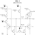
- FIG. 1 illustrates a gate driver that supplies a scan signal to a pixel of an organic light emitting display apparatus, and illustrates one scan circuit.
- the scan circuit of the gate driver generates the scan signal and supplies the scan signal to a scan TFT of a pixel circuit through a gate line.
- a pull-up TFT outputs a high voltage (a gate high voltage) to the gate line
- a pull-down TFT T1 outputs a low voltage (a gate low voltage) to the gate line
- a switching TFT T2 is a reset TFT that shifts a voltage, charged into a Q node, to a low voltage (for example, a ground or VGL).
- the output voltage Vgout denotes a high voltage that is output when the pull-up TFT is turned on.
- the output voltage Vgout should be output at the VGH level, but the output voltage Vout becomes lower than a normal voltage due to the off current (Ioff) of each of the pull-down TFT T1 and the switching TFT T2.
- Ioff off current
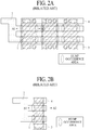
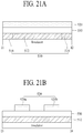
- FIG. 2A is a diagram illustrating a plan layout of a pull-down TFT included in a scan circuit.
- FIG. 2B is a diagram illustrating a plan layout of a reset TFT included in the scan circuit.
- FIG. 2C is a diagram illustrating a plan layout of a driving TFT included in a pixel circuit.
- FIG. 3 illustrates a cross-sectional surface of the pull-down TFT taken along line A1-A2 of FIG. 2A , a cross-sectional surface of the reset TFT taken along line A1-A2 of FIG. 2B , and a problem where a hump occurs in the pull-down TFT and the reset TFT.
- the pull-down TFT and the reset TFT are formed in a coplanar top gate type. Cross-sectional surfaces of the pull-down TFT, the reset TFT, and the driving TFT are similar, and thus, the cross-sectional surface of the driving TFT is not illustrated.
- the pull-down TFT T1 is formed to have a larger area than those of other TFTs, a gate electrode 2 is formed in a double line structure, and a multichannel is formed by overlapping of an active layer 1 and the gate electrode 2.
- a channel area of the active layer 1 contacts a source electrode 3 and a drain electrode 4.
- the switching TFT T2 is formed to have a smaller area than that of the pull-down TFT T1, and a gate electrode 2 is formed in a double line structure for forming a multichannel.
- An active layer 1 is formed in one pattern and contacts a source electrode 3 and a drain electrode 4.
- a gate electrode 2 is formed in a single line structure, and an active layer 1 is formed in one pattern and contacts a source electrode 3 and a drain electrode 4.
- a gate insulator 5 is formed between an active layer 1 and a gate electrode 2.
- Left and right edges of the active layer 1 have a taper form, and thus, a parasitic TFT is formed. That is, the taper forms of the left and right edges of the active layer 1 overlap the gate electrode 2, and thus, the parasitic TFT is formed.
- FIG. 3 although the cross-sectional surface of the driving TFT is not illustrated, identically or similarly to the pull-down TFT T1 and the switching TFT T2, left and right edges of an active layer of the driving TFT have a taper form, and thus, a parasitic TFT is formed.
- threshold voltages Vth1 and Vth3 are lower than a threshold voltage Vth2 of the channel due to the parasitic TFTs which are formed in the left and right edges of the active layer 1.
- the threshold voltages Vth1 and Vth3 are lowered by the parasitic TFTs, strong electric fields are generated in the left and right edges of the active layer 1.
- a current should linearly increase in a section of 0 V to 3 V, but since a strong electric field is generated in an edge area of an active layer, a hump where a current is nonlinearly shifted occurs.
- a delay of a turn-on/off time of a TFT extends, and for this reason, a switching characteristic is degraded.
- a leakage current occurs due to humps caused by the parasitic TFTs of the left and right edges of the active layer 1, an output voltage Vgout of the scan circuit is lowered. Also, the switching TFT of the pixel circuit cannot normally operate (turn on/off), causing a screen defect.
- the present invention is directed to a TFT of a display apparatus that substantially obviates one or more problems due to limitations and disadvantages of the related art.
- An aspect of the present invention is directed to provide a thin film transistor (TFT) that reduces leakage current caused by a hump.
- TFT thin film transistor
- Another aspect of the present invention is directed to a TFT for a display apparatus which prevents an output voltage of a scan circuit from being dropped due to a hump of a TFT included in a scan circuit of a gate driver, thereby preventing a screen defect of the display apparatus.
- Another aspect of the present invention is directed to provide a TFT for a display apparatus which prevents a leakage current (or an off current) from occurring due to a hump of a driving TFT included in a pixel circuit, thereby preventing a screen defect of the display apparatus.
- TFT thin film transistor
- TFT thin film transistor
- a structure for example, an electrode, a line, a wiring, a layer, or a contact
- this description should be construed as including a case where the structures contact each other and moreover a case where a third structure is disposed therebetween.
- first, second, etc. may be used herein to describe various elements, these elements should not be limited by these terms. These terms are only used to distinguish one element from another. For example, a first element could be termed a second element, and, similarly, a second element could be termed a first element, without departing from the scope of the present invention.
- FIG. 4 is a diagram schematically illustrating an organic light emitting display apparatus including a TFT according to an embodiment of the present invention
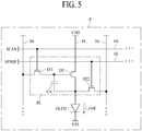
- FIG. 5 is a diagram illustrating one of a plurality of pixels provided in an organic light emitting display apparatus.
- the organic light emitting display apparatus including the TFT includes a display panel and a driving circuit unit that drives the display panel.
- the driving circuit unit may include a data driver, a gate driver, a timing controller, and a memory.
- the timing controller may operate the data driver and the gate driver in a driving mode, based on a timing sync signal TSS. Also, the timing controller may operate the data driver and the gate driver in a sensing mode, based on a timing sync signal TSS and thus cause a threshold voltage/mobility of a driving TFT DT of each of a plurality of sub-pixels to be sensed.
- the gate driver may generate a scan signal SCAN (a gate driving signal) and a sensing signal SENSE according to a gate control signal GCS supplied from the timing controller.
- the gate driver may output the scan signal to a gate line GL and output the generated sensing signal to a sensing signal line SL.
- the gate driver may generate the scan signal SCAN (the gate driving signal) having a gate-on voltage level at every one horizontal period, based on the gate control signal GCS.
- the gate driver may sequentially supply the generated scan signal SCAN to a plurality of the gate lines GL.
- the gate driver may be provided on a substrate of a display panel in a gate-in panel (GIP) type.
- GIP gate-in panel
- the GIP type gate driver may be provided in a non-display area of the substrate.
- the gate driver may be provided in a left or right non-display area of the display panel in the GIP type.
- the gate driver may be provided in each of the left non-display area and the right non-display area of the display panel in the GIP type.
- the scan signal SCAN (the gate driving signal) may have the gate-on voltage level during a data charging period of each of a plurality of sub-pixels P.
- the scan signal SCAN may have a gate-off voltage level during an emission period of each sub-pixel P.
- the gate driver may include a shift register that sequentially outputs the scan signal SCAN.
- the gate driver may be connected to a plurality of driving power lines PL1 to PLm and may supply a driving voltage VDD to the plurality of driving power lines PL1 to PLm. If the driving voltage VDD is output from the gate driver, the plurality of driving power lines PL1 to PLm may be arranged in a horizontal line in the display panel. In FIG. 4 , an example where the plurality of driving power lines PL1 to PLm are arranged in the horizontal line in the display panel is illustrated.
- the data driver may convert input image data into a data voltage Vdata and supply the data voltage Vdata to a data line DL.
- initial compensation data and real-time compensation data may be reflected, and thus, the data voltage Vdata based on image data in which compensation data stored in the memory is reflected may be generated.
- the gate driver has been described as outputting the driving voltage VDD, but the present embodiment is not limited thereto.
- the data driver may output the driving voltage VDD.
- the data driver may be connected to the plurality of driving power lines PL1 to PLm and may supply the driving voltage VDD to the plurality of driving power lines PL1 to PLm. If the driving voltage VDD is output from the data driver, the plurality of driving power lines PL1 to PLm may be arranged in a vertical direction in the display panel.
- the plurality of gate lines GL, a plurality of the sensing signal lines SL, a plurality of the data lines DL, the plurality of driving voltage lines PL, and a plurality of reference voltage lines RL may be disposed in the display panel.
- the plurality of sub-pixels P may be defined by the lines GL, SL, DL, PL and RL.
- Each of the plurality of sub-pixels P may include an organic light emitting diode OLED and a pixel circuit PC that emits the organic light emitting diode OLED.
- Each of the plurality of sub-pixels P may be one of a red sub-pixel, a green sub-pixel, a blue sub-pixel, and a white sub-pixel.
- the one pixel may be configured with a red sub-pixel, a green sub-pixel, a blue sub-pixel, and a white sub-pixel.
- the plurality of gate lines GL and the plurality of sensing signal lines SL may be arranged in parallel in a first direction (for example, the horizontal direction) in the display panel.
- the scan signal (the gate driving signal) may be applied from the data driver to the gate lines GL.
- the sensing signals SENSE may be applied from the gate driver to the sensing signal lines SL.
- the plurality of driving voltage lines PL may be arranged in parallel with the gate lines GL.
- a high-level driving voltage VDD may be supplied to the sub-pixels P through the driving power lines PL.
- the plurality of data lines DL may be arranged in a second direction (for example, the vertical direction) to intersect the plurality of gate lines GL and the plurality of sensing signal lines SL.
- the data voltage Vdata may be supplied from the data driver to the data line DL.
- the data voltage Vdata may have a voltage level in which a compensation voltage corresponding to a shift of a threshold voltage (Vth) of the driving TFT DT of a corresponding sub-pixel P is reflected.
- the plurality of reference voltage lines RL may be arranged in parallel with the plurality of data lines DL.
- a reference voltage or a sensing precharging voltage may be selectively supplied from the data driver to the reference voltage lines RL.
- the pixel circuit PC of each sub-pixel P may include a first switching TFT ST1, a second switching TFT ST2, a driving TFT DT, and a storage capacitor Cst.
- the TFTs ST1, ST2 and DT included in the pixel circuit PC and a plurality of TFTs included in a scan circuit of the gate driver may be each implemented in an N type or a P type where an active layer is formed of low-temperature poly silicon (LTPS).
- LTPS low-temperature poly silicon
- the present embodiment is not limited thereto.
- the first switching TFT ST1 may be turned on according to the scan signal having the gate-on voltage level supplied to the gate line GL.
- the data voltage Vdata supplied to the data line DL may be supplied to a gate electrode of the driving TFT DT.
- the second switching TFT ST2 may be turned on according to the sensing signal SENSE having the gate-on voltage level supplied to the sensing signal line SL.
- a display reference voltage or the sensing precharging voltage supplied to the reference voltage line RL may be supplied to a node disposed between the driving TFT DT and the organic light emitting diode OLED.
- the driving TFT DT may be turned on by a voltage charged into the capacitor Cst at every emission period and may control an amount of current flowing from a first driving voltage source VDD to the organic light emitting diode OLED.
- the organic light emitting diode OLED may emit single-color light, having luminance corresponding to the data current Ioled, with a data current Ioled supplied from the driving TFT DT of the pixel circuit PC.
- FIG. 6 illustrates a plan layout of a TFT 100 according to a first embodiment of the present invention and is a diagram illustrating a plan layout of a pull-down TFT among a plurality of buffer TFTs included in a scan circuit of a gate driver.
- FIG. 8A is a diagram illustrating a cross-sectional surface of a pull-down TFT taken along lines B1-B2 and C1-C2 of FIG. 6 .
- the TFT 100 according to the first embodiment of the present invention may be applied to a plurality of buffer TFTs (a pull-up TFT and a pull-down TFT) of a scan circuit.
- a pull-up TFT and a pull-down TFT a pull-up TFT and a pull-down TFT
- T1 of FIG. 1 a pull-down TFT among the buffer TFTs of the scan circuit
- the pull-down TFT of the scan circuit may be implemented to have a larger area than those of general switching TFTs so as not to be deteriorated by a high voltage and long-time driving.
- the gate electrode 120 may be formed in a double line structure for forming a multichannel, and an active layer 110 may be patterned for forming a plurality of channels.
- the TFT 100 may be formed in a top gate structure.
- the active layer 110 may be formed on a substrate, and a gate insulator 150 may be formed on the active layer 110.
- the gate electrode 120 may be formed on the gate insulator 150.
- the gate electrode 120 may branch as two lines from a gate line and may be long formed in a horizontal direction.
- a source electrode 130 may be disposed under the gate electrode 120, and a drain electrode 140 may be disposed on the gate electrode 120.
- the present embodiment is not limited thereto.
- the drain electrode 140 may be disposed under the gate electrode 120, and the source electrode 130 may be disposed on the gate electrode 120.
- the active layer 110 may be formed to overlap the gate electrode 120, and a channel area of the active layer 110 may contact the source electrode 130 and the drain electrode 140.
- the gate electrode 120 may not wholly overlap the active layer 110, and the gate electrode 120 may partially overlap the active layer 110.
- the source electrode 130 and the drain electrode 140 may be respectively disposed at both ends of the active layer 110.
- the source electrode 130 may be connected to a data line through a contact metal which is provided in a contact hole, and the drain electrode 140 may be connected to an anode electrode (or a signal line) of an organic light emitting diode (OLED).
- OLED organic light emitting diode
- the active layer 110 may include a plurality of channel areas 112, a dummy area 114 which is disposed at each of a left edge and a right edge of each of the plurality of channel areas 112, and a plurality of link areas 116 which are disposed between the plurality of channel areas 112.
- the active layer 110 may be formed of low-temperature poly silicon (LTPS), but is not limited thereto.
- the active layer 110 may be formed of amorphous silicon (a-Si), poly-Si, oxide, an organic material, or the like.
- the plurality of channel areas 112 may overlap the gate electrode 120 for forming a multichannel and may be disposed between the source electrode 130 and the drain electrode 140.
- the plurality of link areas 116 may be respectively disposed between the plurality of channel areas 112 and may connect the plurality of channel areas 112. That is, the plurality of channel areas 112 may be connected in one pattern by the plurality of link areas 116.
- Each of the plurality of link areas 116 may include a slit, and the slit may be disposed to overlap a portion corresponding to a space between two lines of the gate electrode 120.
- the plurality of channel areas 112 and the plurality of link areas 116 may be formed by patterning a conductive transparent material (for example, indium tin oxide (ITO) or the like) layer. Therefore, the plurality of channel areas 112 and the plurality of link areas 116 may be formed of the same material.
- a conductive transparent material for example, indium tin oxide (ITO) or the like
- a width of each of the plurality of link areas 116 may be formed less than a vertical-direction width of each of the two lines of the gate electrode 120.
- the dummy area 114 may be disposed to extend from the left edge and right edge of the channel area 112 to an outer portion through an end of the gate electrode 120. That is, the dummy area 114 may protrude from the left edge and right edge of the channel area 112 and extend to a left outer portion and a right outer portion of the channel area 112. Therefore, the left edge and right edge of the active layer 110 may not overlap the gate electrode 120.
- an end of the dummy area 114 may be disposed at the outer portion of the gate electrode 120, and in detail, the end of the dummy area 114 may be disposed at a position which is separated from the edge of the gate electrode 120 by a certain distance. That is, the end of the dummy area 114 may be disposed to be separated from the edge of the gate electrode 120 by a certain interval.
- the dummy area 114 may protrude to the outer portion of the gate electrode 120 by a length W2 corresponding to 10% to 30% of a width W1 of the gate electrode 120. That is, an end of the dummy area 114 may be disposed to be separated from an edge of the gate electrode 120 by an interval equal to the length W2 corresponding to 10% to 30% of the width W1 of the gate electrode 120.
- the dummy area 114 may protrude to the outer portion of the gate electrode 120 by a length W2 corresponding to 10% to 30% of a width W1 of a portion where the gate electrode 120 overlaps the active layer 110. That is, the end of the dummy area 114 may be disposed to be separated from the edge of the gate electrode 120 by an interval equal to the length W2 corresponding to 10% to 30% of the width W1 of the portion where the gate electrode 120 overlaps the active layer 110.
- a length by which the dummy area 114 protrudes may be set in consideration of an overlap margin of the gate electrode 120 and the active layer 110. Therefore, a numerical value of the length by which the dummy area 114 protrudes is not limited to the length W2 corresponding to 10% to 30% of the width W1 of the gate electrode 120 or the length W2 corresponding to 10% to 30% of the width W1 of the portion where the gate electrode 120 overlaps the active layer 110.
- the dummy area 114 may not protrude to the outer portion of the gate electrode 120. That is, the dummy area 114 may not normally be formed.
- the length by which the dummy area 114 protrudes is too longer set (for example, more than 30% of the width W1 of the gate electrode 120 or more than 30% of the width W1 of the portion where the gate electrode 120 overlaps the active layer 110), a size of the dummy area 114 increases, and for this reason, a whole size of a TFT increases. For this reason, all TFTs cannot be provided in a limited space, namely, a designing space is limited.
- the dummy area 114 protrudes to the outer portion of the gate electrode 120 by the length W2 corresponding to a maximum of 30% of the width W1 of the gate electrode 120 in consideration of the design of the pull-down TFT configuring the scan circuit and a manufacturing process margin.
- the dummy area 114 protrudes to the outer portion of the gate electrode 120 by the length W2 corresponding to a maximum of 30% of the width W1 of the portion where the gate electrode 120 overlaps the active layer 110, in consideration of the design of a TFT and a manufacturing process margin.
- a gate insulator 150 may be formed on a left end and a right end of the active layer 110.
- the gate electrode 120 may not be disposed on the left end and right end (the end of the dummy area 114) of the active layer 110. Therefore, the edge of the active layer 110 does not overlap the gate electrode 120, and thus, a parasitic TFT caused by an overlap of a gate electrode and an edge of an active layer in the related art cannot be formed in the present invention. For example, even when the parasitic TFT is formed, the parasitic TFT is very small in size.
- a hump is prevented from occurring due to a parasitic TFT which is formed in the buffer TFTs of the scan circuit, and thus, an output characteristic of the buffer TFTs of the scan circuit is enhanced. If the output characteristic of the buffer TFTs of the scan circuit is enhanced, a screen defect of a display apparatus cannot occur, and thus, display quality is enhanced.
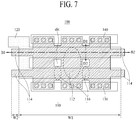
- FIG. 7 illustrates a plan layout of a TFT 100 according to a second embodiment of the present invention and is a diagram illustrating a plan layout of a pull-down TFT among a plurality of buffer TFTs included in a scan circuit of a gate driver.
- FIG. 8B is a diagram illustrating a cross-sectional surface of a pull-down TFT taken along lines B1-B2 and D1-D2 of FIG. 7 .
- a gate electrode 120 may be formed in a double line structure for forming a multichannel, and an active layer 110 may be patterned for forming a plurality of channels.
- the gate electrode 120 may branch as two lines from a gate line and may be long formed in a horizontal direction.
- a source electrode 130 may be disposed under the gate electrode 120, and a drain electrode 140 may be disposed on the gate electrode 120.
- the active layer 110 may be disposed to overlap the gate electrode 120 and may contact the source electrode 130 and the drain electrode 140.
- the present embodiment is not limited thereto.
- the drain electrode 140 may be disposed under the gate electrode 120, and the source electrode 130 may be disposed on the gate electrode 120.
- a plurality of channel areas 112 of the active layer 110 may overlap the gate electrode 120 for forming a multichannel and may be disposed between the source electrode 130 and the drain electrode 140.
- the gate electrode 120 may not wholly overlap the active layer 110, and the gate electrode 120 may partially overlap the active layer 110.
- a plurality of link areas 116 of the active layer 110 may be respectively disposed between the plurality of channel areas 112 and may connect the plurality of channel areas 112. That is, the plurality of channel areas 112 may be connected in one pattern by the plurality of link areas 116. In this case, a width of each of the plurality of link areas 116 may be formed greater than a vertical-direction width of each of two lines of the gate electrode 120.
- Each of the plurality of link areas 116 may include a slit, and the slit may be disposed to overlap a portion corresponding to a space between the two lines of the gate electrode 120.
- a dummy area 114 of the active layer 110 may be disposed to extend from a left edge and a right edge of the channel area 112 to an outer portion through an end of the gate electrode 120. That is, the dummy area 114 may protrude from the left edge and right edge of the channel area 112, and ends of the dummy area 114 may be respectively disposed at a left outer portion and a right outer portion of the channel area 112. Therefore, the left edge and right edge (the dummy area 114) of the active layer 110 may not overlap the gate electrode 120.
- the ends of the dummy area 114 may be disposed at the outer portion of the gate electrode 120, and in detail, the ends of the dummy area 114 may be respectively disposed at positions which are separated from the edge of the gate electrode 120 by a certain distance.
- the dummy area 114 may protrude to the outer portion of the gate electrode 120 by a length W2 corresponding to 10% to 30% of a width W1 of the gate electrode 120. That is, the ends of the dummy area 114 may be disposed to be separated from an edge of the gate electrode 120 by an interval equal to the length W2 corresponding to 10% to 30% of the width W1 of the gate electrode 120.
- the dummy area 114 may protrude to the outer portion of the gate electrode 120 by a length W2 corresponding to 10% to 30% of a width W1 of a portion where the gate electrode 120 overlaps the active layer 110. That is, the ends of the dummy area 114 may be disposed to be separated from the edge of the gate electrode 120 by an interval equal to the length W2 corresponding to 10% to 30% of the width W1 of the portion where the gate electrode 120 overlaps the active layer 110.
- a length of the dummy area 114 protruding from the channel area 112 is not limited to 10% to 30% of the width W1 of the gate electrode 120. It is set by the inventors that the dummy area 114 protrudes to the outer portion of the gate electrode 120 by a length corresponding to a maximum of 30% of the width W1 of the gate electrode 120 in consideration of the design of the pull-down TFT configuring the scan circuit and a manufacturing process margin.
- a length of the dummy area 114 protruding from the channel area 112 is not limited to 10% to 30% of the width W1 of the portion where the gate electrode 120 overlaps the active layer 110. It is set by the inventors that the dummy area 114 protrudes to the outer portion of the gate electrode 120 by a length W2 corresponding to a maximum of 30% of the width W1 of the gate electrode 120 in consideration of the design of the pull-down TFT configuring the scan circuit and a manufacturing process margin.
- a gate insulator 150 may be formed on a left end and a right end of the active layer 110.
- the gate electrode 120 may not be disposed on the left end and right end (an end of the dummy area 114) of the active layer 110. Therefore, an edge of the active layer 110 does not overlap the gate electrode 120, and thus, a parasitic TFT caused by an overlap of a gate electrode and an edge of an active layer in the related art cannot be formed. For example, even when the parasitic TFT is formed, the parasitic TFT is very small in size.
- a hump is prevented from occurring due to a parasitic TFT which is formed in the buffer TFTs of the scan circuit, and thus, an output characteristic of the buffer TFTs of the scan circuit is enhanced. If the output characteristic of the buffer TFTs of the scan circuit is enhanced, a screen defect of a display apparatus cannot occur, and thus, display quality is enhanced.
- a parasitic TFT cannot be formed at the left end and right end of the active layer 110, or the number of parasitic TFTs is minimized.
- a pattern of the active layer 110 may be changed in order for the edge of the active layer 110 to extend to the outer portion of the gate electrode 120, namely, the dummy area 114 may be provided, and thus, an area where a parasitic TFT is formed is removed or minimized.
- the edge of the gate electrode 120 may be disposed in a diagonal direction from the left edge and right edge (the dummy area 114) of the active layer 110. However, the left edge and right edge (the dummy area 114) of the active layer 110 and the gate electrode 120 may be disposed to be separated from each other by a long distance with the gate insulator 150 therebetween. Therefore, even when a parasitic TFT is formed, the parasitic TFT is very small in size, and thus, a hump is prevented from occurring due to the parasitic TFT, or the number of humps is reduced.
- threshold voltages Vth1 and Vth3 of parasitic TFTs may have larger values than that of a threshold voltage Vth2 of the channel area 112 of the active layer 110.
- parasitic TFTs having a small size may be respectively formed at the left edge and right edge of the active layer 110, and threshold voltages Vth1 and Vth3 of the parasitic TFTs may have large values. Therefore, a hump is prevented from occurring in the left edge and right edge of the active layer 110, and a strong electric field is not generated in an edge area of the active layer 110.
- the TFT 100 according to the first and second embodiments of the present invention is applied to the buffer TFTs (in detail, the pull-down TFT) of the scan circuit of the gate driver, a leakage current (or an off current) is prevented from occurring in the scan circuit or is reduced. Accordingly, a signal is normally output through the Q node and QB node of the scan circuit, and thus, a screen defect of a display apparatus is prevented.
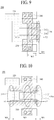
- FIG. 9 illustrates a plan layout of a TFT 200 according to a third embodiment of the present invention and is a diagram illustrating a plan layout of a switching TFT, included in a scan circuit of a gate driver, or a switching TFT included in a pixel circuit.
- FIG. 11A is a diagram illustrating a cross-sectional surface, taken along line E1-E2 of FIG. 9 , of a switching TFT included in a scan circuit or a switching TFT included in a pixel circuit.
- the TFT 200 according to the third embodiment of the present invention may be applied to a switching TFT (T2 (a reset TFT) of FIG. 1 ) of a scan circuit.
- the switching TFT of the scan circuit should quickly operate in response to an input signal and thus may be formed to have a smaller area than that of a buffer TFT.
- the TFT 200 according to a third embodiment of the present invention may be applied to a switching TFT of a pixel circuit.
- the switching TFT of the pixel circuit should quickly operate in response to an input signal and thus may be formed to have a smaller area than that of a driving TFT.
- a gate electrode 220 may be formed in a double line structure for forming a multichannel, and an active layer 210 may be patterned for forming a plurality of channels.
- the gate electrode 220 may branch as two lines from a gate line and may be long formed in a horizontal direction.
- a source electrode 230 may be disposed under the gate electrode 220, and a drain electrode 240 may be disposed on the gate electrode 220.
- the present embodiment is not limited thereto.
- the drain electrode 240 may be disposed under the gate electrode 220, and the source electrode 230 may be disposed on the gate electrode 220.
- the active layer 210 may be disposed to overlap the gate electrode 220 and may contact the source electrode 230 and the drain electrode 240.
- a channel area may be disposed between the source electrode 230 and the drain electrode 240.
- the gate electrode 220 may not wholly overlap the active layer 210, and the gate electrode 220 may partially overlap the active layer 210.
- the TFT 200 may be formed in a top gate structure. Therefore, the active layer 210 may be formed on a substrate, and a gate insulator 250 may be formed on the active layer 210. The gate electrode 220 may be formed on the gate insulator 250.
- the active layer 210 may include a channel area 212 and a dummy area 214 which is disposed at a right edge of the channel area 212.
- the dummy area 214 is illustrated as being disposed at the right edge of the channel area 212, but this is merely an example. In another embodiment of the present invention, the dummy area 214 may be disposed at a left edge of the channel area 212.
- the active layer 210 may be formed of low-temperature poly silicon (LTPS), but is not limited thereto.
- the active layer 210 may be formed of amorphous silicon (a-Si), poly-Si, oxide, an organic material, or the like.
- the channel area 212 may overlap the gate electrode 220 for forming a multichannel and may be disposed between the source electrode 230 and the drain electrode 240.
- the gate electrode 220 may be disposed in a double line structure, and the active layer 210 may be disposed to overlap two lines of the gate electrode 220, whereby the multichannel is formed in the channel area 212.
- the dummy area 214 may be disposed to extend from a right edge of the channel area 212 to an outer portion of an end of the gate electrode 220. That is, the dummy area 214 may protrude from one side edge (a right edge) of the channel area 212, and an end of the dummy area 214 may be disposed at one side outer portion (a right outer portion) of the channel area 212. Therefore, the right edge of the active layer 210 may not overlap the gate electrode 220.
- the end of the dummy area 214 may be disposed at the outer portion of the gate electrode 220. Therefore, the end of the dummy area 214 may be disposed to be separated from the edge of the gate electrode 220 by a certain distance.
- the dummy area 214 may protrude to the outer portion of the gate electrode 220 by a length W4 corresponding to 10% to 30% of a width W3 of a portion where the gate electrode 220 overlaps active layer 210. That is, the end of the dummy area 214 may be disposed to be separated from an edge of the gate electrode 220 by an interval equal to the length W4 corresponding to 10% to 30% of the width W3 of the portion where the gate electrode 220 overlaps active layer 210.
- a length of the dummy area 214 protruding from the channel area 212 is not limited to 10% to 30% of the width W3 of the portion where the gate electrode 220 overlaps the active layer 210. It is set by the inventors that the dummy area 214 protrudes to the outer portion of the gate electrode 220 by a length W4 corresponding to a maximum of 30% of the width W3 of the portion where the gate electrode 220 overlaps the active layer 210, in consideration of the design of a switching TFT configuring a scan circuit and a manufacturing process margin.
- the gate insulator 250 may be formed on a right end of the active layer 210.
- the gate electrode 220 may not be disposed on the right end of the active layer 210. Therefore, a parasitic TFT caused by an overlap of a gate electrode and an edge of an active layer in the related art cannot be formed in the present invention. For example, even when the parasitic TFT is formed, the parasitic TFT is very small in size.
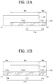
- FIG. 10 illustrates a plan layout of a TFT 300 according to a fourth embodiment of the present invention and is a diagram illustrating a plan layout of a switching TFT, included in a scan circuit of a gate driver, or a switching TFT included in a pixel circuit.
- FIG. 11B is a diagram illustrating a cross-sectional surface, taken along line F11-F12 of FIG. 10 , of a switching TFT included in a scan circuit or a switching TFT included in a pixel circuit.
- a gate electrode 320 may be formed in a double line structure for forming a multichannel, and an active layer 310 may be patterned for forming a plurality of channels.
- the gate electrode 320 may branch as two lines from a gate line and may be long formed in a horizontal direction.
- a source electrode 330 may be disposed under the gate electrode 320, and a drain electrode 340 may be disposed on the gate electrode 320.
- the present embodiment is not limited thereto.
- the drain electrode 340 may be disposed under the gate electrode 320, and the source electrode 330 may be disposed on the gate electrode 320.
- the active layer 310 may be disposed to overlap the gate electrode 320, and a channel area of the active layer 310 may contact the source electrode 330 and the drain electrode 340.
- the active layer 310 may overlap two lines of the gate electrode 320 for forming a multichannel, and the channel area may be disposed between the source electrode 330 and the drain electrode 340.
- the gate electrode 320 may not wholly overlap the active layer 310, and the gate electrode 320 may partially overlap the active layer 310.
- the dummy area 314 of the active layer 310 may be disposed to extend from a left edge and a right edge of the channel area 312 to an outer portion of an end of the gate electrode 320. That is, the dummy area 314 may protrude from the left edge and right edge of the channel area 312, and an end of the dummy area 314 may be disposed at a left outer portion and a right outer portion of the channel area 312. Therefore, the left edge and right edge of the active layer 310 may not overlap the gate electrode 320.
- the end of the dummy area 314 may be disposed at the outer portion of the gate electrode 320. Therefore, the end of the dummy area 314 may be disposed at a position which is separated from the left edge and right edge of the gate electrode 320 by a certain distance.
- the dummy area 314 may protrude to the outer portion of the gate electrode 320 by a length W6 corresponding to 10% to 30% of a width W5 of a portion where the gate electrode 320 overlaps active layer 310. That is, the end of the dummy area 314 may be disposed to be separated from an edge of the gate electrode 320 by an interval equal to the length W6 corresponding to 10% to 30% of the width W5 of the portion where the gate electrode 320 overlaps active layer 310.
- a length of the dummy area 314 protruding from the channel area 312 is not limited to 10% to 30% of the width W5 of the portion where the gate electrode 320 overlaps the active layer 310. It is set by the inventors that the dummy area 314 protrudes to the outer portion of the gate electrode 320 by a length W6 corresponding to a maximum of 30% of the width W5 of the portion where the gate electrode 320 overlaps the active layer 310, in consideration of the design of a switching TFT configuring a scan circuit or the design of a switching TFT configuring a pixel circuit and a manufacturing process margin.
- a parasitic TFT cannot be formed at the left end and right end of the active layer 310, or the number of parasitic TFTs is minimized.
- a pattern of the active layer 310 may be changed in order for the edge of the active layer 310 to extend to the outer portion of the gate electrode 320, and thus, an area where a parasitic TFT is formed is removed or minimized.
- the edge of the gate electrode 320 may be disposed in a diagonal direction from the left edge and right edge (the dummy area 314) of the active layer 310. However, the left edge and right edge (the dummy area 314) of the active layer 310 and the gate electrode 320 may be disposed to be separated from each other by a long distance with the gate insulator 350 therebetween. Therefore, even when a parasitic TFT is formed, the parasitic TFT is very small in size, and thus, a hump is prevented from occurring due to the parasitic TFT, or the number of humps is reduced.
- threshold voltages Vth1 and Vth3 of parasitic TFTs may have larger values than that of a threshold voltage Vth2 of the channel area 312 of the active layer 310.
- parasitic TFTs having a small size may be respectively formed at the left edge and right edge of the active layer 310, and threshold voltages Vth1 and Vth3 of the parasitic TFTs may have large values. Therefore, a hump is prevented from occurring in the left edge and right edge of the active layer 310, and a strong electric field is not generated in an edge area of the active layer 310.
- the TFT according to the third and fourth embodiments of the present invention is applied to a switching TFT of a scan circuit of a gate driver, a leakage current (or an off current) of the switching TFT is reduced. Accordingly, a signal is normally output through a Q node and a QB node of the scan circuit, and thus, a screen defect of a display apparatus is prevented.
- the TFT according to the third and fourth embodiments of the present invention is applied to the switching TFT of the pixel circuit illustrated in FIG. 5 , a leakage current (or an off current) of the switching TFT of the pixel circuit is reduced, and thus, the pixel circuit is prevented from being abnormally driven. Accordingly, a data voltage is supplied to the driving TFT DT during a turn-off period of the organic light emitting diode OLED, thereby preventing a screen defect.
- FIG. 12 is a diagram showing effects where, by changing a pattern of an active layer of a TFT according to first to fourth embodiments of the present invention, an output characteristic of the TFT is enhanced, and humps are reduced.
- the TFT according to the first and second embodiments of the present invention may be applied to the pull-down TFT (T1 of FIG. 1 ) of the scan circuit
- the TFT according to the third and fourth embodiments of the present invention may be applied to the switching TFT (T2 of FIG. 1 ) of the scan circuit and the switching TFT (ST1 or ST2 of FIG. 5 ) of the pixel circuit.
- a flatband voltage Vfb and a threshold voltage Vth of a TFT may increase.
- an on current Ion may increase.
- a hump is prevented from occurring due to a strong electric field which is generated from an edge of an active layer of a TFT, and thus, a leakage current is reduced. Accordingly, a screen defect of a display apparatus is prevented, and thus, display quality is enhanced.
- FIG. 13 illustrates a plan layout of a TFT 400 according to a fifth embodiment of the present invention and is a diagram illustrating a plan layout of a driving TFT included in a pixel circuit.
- FIG. 14 is a diagram illustrating a cross-sectional surface of a driving TFT taken along line G1-G2 of FIG. 13 .
- the TFT 400 according to the fifth embodiment of the present invention may be applied to a driving TFT (DT of FIG. 5 ) of a pixel circuit.
- a gate electrode 420 of the TFT 400 may be formed by branching from a gate line.
- a source electrode 430 may be disposed under the gate electrode 420, and a drain electrode 440 may be disposed on the gate electrode 420.
- the present embodiment is not limited thereto.
- the drain electrode 440 may be disposed under the gate electrode 420, and the source electrode 430 may be disposed on the gate electrode 420.
- An active layer 410 may be formed to overlap the gate electrode 420.
- the TFT 400 according to the fifth embodiment of the present invention may be formed in a top gate structure.
- the active layer 410 may be formed on a substrate, and a gate insulator 450 may be formed on the active layer 410.
- the gate electrode 420 may be formed on the gate insulator 450.
- the active layer 410 may include a channel area 412 and a dummy area 414 which is disposed at an edge of the channel area 412.
- the active layer 410 may be formed of low-temperature poly silicon (LTPS), but is not limited thereto.
- the active layer 410 may be formed of amorphous silicon (a-Si), poly-Si, oxide, an organic material, or the like.
- a portion of the active layer 410 overlapping the gate electrode 420 may be the channel area 412. That is, the channel area 412 may overlap the gate electrode 420.
- the channel area 412 may be disposed between the source electrode 430 and the drain electrode 440.
- the dummy area 414 of the active layer 410 may be disposed to extend from a right edge of the channel area 412 to an outer portion of the gate electrode 420. That is, the dummy area 414 may protrude from one side edge (a right edge) of the channel area 412, and an end of the dummy area 414 may be disposed at one side outer portion (a right outer portion) of the channel area 412. Therefore, the right edge of the active layer 410 may not overlap the gate electrode 420.
- the present embodiment is not limited thereto.
- the dummy area 414 may protrude from a left edge of the channel area 412, and the end of the dummy area 414 may be disposed at a left outer portion of the channel area 412. In this case, the left edge of the active layer 410 may not overlap the gate electrode 420.
- the end of the dummy area 414 may be disposed at the left or right edge of the gate electrode 420. Therefore, the end of the dummy area 414 may be disposed at a position which is separated from the left or right edge of the gate electrode 420 by a certain distance.
- the dummy area 414 may protrude to an outer portion through an end of the gate electrode 420 by a length W8 corresponding to 50% to 100% of a width W7 of a portion where the gate electrode 420 overlaps active layer 410. That is, the end of the dummy area 414 may be disposed to be separated from an edge of the gate electrode 420 by an interval equal to the length W8 corresponding to 50% to 100% of the width W7 of the portion where the gate electrode 420 overlaps active layer 410.
- a length of the dummy area 414 protruding from the channel area 412 is not limited to 50% to 100% of the width W7 of the portion where the gate electrode 420 overlaps active layer 410. It is set by the inventors that the dummy area 414 protrudes to the outer portion of the gate electrode 420 by a length W8 corresponding to a maximum of 100% of the width W7 of the portion where the gate electrode 420 overlaps the active layer 410, in consideration of the design of a driving TFT configuring a pixel circuit and a manufacturing process margin.
- the gate insulator 450 may be formed on a right end of the active layer 410.
- the gate electrode 420 may not be disposed on the right end of the active layer 410. Therefore, an edge of the active layer 410 does not overlap the gate electrode 420, and thus, a parasitic TFT caused by an overlap of a gate electrode and an edge of an active layer in the related art cannot be formed in the present invention. For example, even when the parasitic TFT is formed, the parasitic TFT is very small in size.
- a parasitic TFT cannot be formed at one side end of the active layer 410, or the number of parasitic TFTs is minimized.
- a pattern of the active layer 410 may be changed in order for the edge of the active layer 410 to extend to one side outer portion of the gate electrode 420, and thus, an area where a parasitic TFT is formed is removed or minimized.
- the edge of the gate electrode 420 may be disposed in a diagonal direction from one side edge of the active layer 410. However, an interval between the active layer 410 and the gate electrode 420 which are disposed with the gate insulator 450 therebetween is large, and thus, a parasitic TFT is very small in size.
- a threshold voltage Vth1 of a parasitic TFT may have a larger value than that of a threshold voltage Vth2 of the channel area 412 of the active layer 410.
- a parasitic TFT having a small size may be formed at one side edge of the active layer 410, and a threshold voltage Vth1 of the parasitic TFT may have a large value. Therefore, a hump is prevented from occurring in the left edge and right edge of the active layer 410. Also, a strong electric field is not generated in an edge area of the active layer 410.
- the TFT according to the fifth embodiment of the present invention is applied to a driving TFT (DT of FIG. 5 ) of a pixel circuit, a hump is prevented from occurring due to a parasitic TFT which is formed in the driving TFT of the pixel circuit, and thus, an output characteristic of the driving TFT is enhanced. Also, a leakage current (or an off current) of the driving TFT is reduced, and thus, a screen defect is prevented from occurring due to weak light which is emitted during a turn-off period of an organic light emitting diode OLED, thereby enhancing the display quality of a display apparatus.
- FIG. 15 is a diagram illustrating a pull-down TFT of a scan circuit, a switching TFT (a reset TFT) of the scan circuit, or a switching TFT of a pixel circuit formed in a single gate (top gate) structure, and a channel formed in an active layer.
- a substrate of a display apparatus is not illustrated.
- the TFT according to the first to fifth embodiments of the present invention may be formed in a top gate structure where one gate electrode is disposed on an active layer.
- an active layer 110 may be disposed on an insulator, and a gate insulator 150 may be disposed on the active layer 110.
- a gate electrode 120 may be disposed on the gate insulator 150.
- the gate electrode 120 may be disposed on the active layer 110 to overlap the active layer 110, and thus, a channel 170 may be formed on a top of the active layer 110.
- the pull-down TFT of the scan circuit, the switching TFT of the scan circuit, and the switching TFT of the pixel circuit described above in the first to fourth embodiments of the present invention may be formed in a top gate structure where one gate electrode is disposed on an active layer.
- a flatband voltage Vfb and a threshold voltage Vth of each of the pull-down TFT of the scan circuit, the switching TFT of the scan circuit, and the switching TFT of the pixel circuit may increase.
- a hump is prevented from occurring due to a strong electric field which is generated from an edge of an active layer of a TFT, and thus, a leakage current is reduced. Accordingly, a screen defect of a display apparatus is prevented, and thus, display quality is enhanced.
- the driving TFT of the pixel circuit described above in the fifth embodiment of the present invention may be formed in a top gate structure where one gate electrode is disposed on an active layer.
- FIG. 16 is a diagram showing effects where, by changing a pattern of an active layer of a driving TFT according to a fifth embodiment of the present invention, an output characteristic of the driving TFT is enhanced, and humps are reduced.
- a flatband voltage Vfb and a threshold voltage Vth of a TFT may increase, and an on current Ion may increase. Therefore, a hump is prevented from occurring due to a strong electric field which is generated from the edge of the active layer 410 of the TFT, and thus, a leakage current is reduced. Accordingly, a screen defect of a display apparatus is prevented, and thus, display quality is enhanced.
- FIG. 17A is a diagram illustrating a pull-down TFT of a scan circuit, a switching TFT (a reset TFT) of the scan circuit, or a driving TFT of a pixel circuit formed in a double gate structure, and a plurality of channels formed in an active layer.
- FIG. 17B is a cross-sectional view, taken along line H1-H2 of FIG. 17A , of a pull-down TFT of a scan circuit, a switching TFT (a reset TFT) of the scan circuit, a switching TFT of a pixel circuit, or a driving TFT of the pixel circuit.
- the TFT according to the first to fifth embodiments of the present invention may be formed in a double gate structure where a gate electrode is disposed under an active layer and another gate electrode is disposed on the active layer.
- an active layer 170 may be disposed on an insulator, and a gate insulator 150 may be disposed on the active layer 170.
- An upper gate electrode 160 (a first gate electrode) may be disposed on the gate insulator 150.
- a lower gate electrode 180 (a second gate electrode) may be disposed under the insulator.
- the upper gate electrode 160 may be electrically connected to the lower gate electrode 180 through a contact.
- the upper gate electrode 160 and the lower gate electrode 180 may be formed in the same shape and may be disposed with the active layer 170 therebetween. In this case, an interval between an edge of the upper gate electrode 160 and an end of a dummy area may be the same as an interval between an edge of the lower gate electrode 180 and the end of the dummy area.
- the present embodiment is not limited thereto.
- the upper gate electrode 160 and the lower gate electrode 180 may be formed in different shapes.
- the end of the dummy area may be separated from the upper gate electrode 160 by a first interval
- the end of the dummy area may be separated from the lower gate electrode 180 by a second interval. That is, the interval between the edge of the upper gate electrode 160 and the end of the dummy area may differ from the interval between the edge of the lower gate electrode 180 and the end of the dummy area.
- the first interval by which the end of the dummy area is separated from the upper gate electrode 160 and the second interval by which the end of the dummy area is separated from the lower gate electrode 180 may be adjusted.
- the active layer 170 may include a plurality of channel areas 172 and a plurality of link areas 174 which are disposed between the plurality of channel areas 172.
- the active layer 170 may be formed of low-temperature poly silicon (LTPS), but is not limited thereto.
- the active layer 170 may be formed of amorphous silicon (a-Si), poly-Si, oxide, an organic material, or the like.
- the plurality of channel areas 172 may be disposed between the upper gate electrode 160 and the lower gate electrode 180.
- the plurality of link areas 174 may be respectively disposed between the plurality of channel areas 172 and may connect the plurality of channel areas 172. That is, the plurality of channel areas 172 may be connected in one pattern by the plurality of link areas 174.
- Each of the plurality of link areas 174 may include a slit.
- the slit may be disposed to overlap a portion corresponding to a space between two lines of the upper gate electrode 160. Also, the slit may be disposed to overlap a portion corresponding to a space between two lines of the lower gate electrode 180.
- the plurality of channel areas 172 and the plurality of link areas 174 may be formed by patterning a conductive transparent material (for example, indium tin oxide (ITO) or the like) layer. Therefore, the plurality of channel areas 172 and the plurality of link areas 174 may be formed of the same material.
- a conductive transparent material for example, indium tin oxide (ITO) or the like
- the upper gate electrode 160 may be disposed on the active layer 170 to overlap the active layer 170, and thus, a first channel 170a may be formed on a top of the active layer 170.
- the lower gate electrode 180 may be disposed under the active layer 170 to overlap the active layer 170, and thus, a second channel 170b may be formed on a bottom of the active layer 170.
- a channel may be formed on each of the top and bottom of the active layer 170, and thus, the active layer 170 may include a plurality of channels 170a and 170b.
- a TFT having the double gate structure is two times the number of channels, namely, two times a width of a channel, and thus, an output characteristic of the TFT is enhanced.
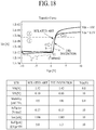
- FIG. 18 is a diagram showing effects where, when a pattern of an active layer of a TFT according to embodiments of the present invention is changed and a multi-gate structure is applied, an output characteristic of the TFT is enhanced, and humps are reduced.
- a pull-down TFT of a scan circuit, a switching TFT (a reset TFT) of the scan circuit, a switching TFT of a pixel circuit, and a driving TFT of the pixel circuit may be formed in the double gate structure, thereby preventing a hump from occurring.
- a TFT is formed in the double gate structure, a flatband voltage Vfb and a threshold voltage Vth of the TFT may increase. Also, an on current Ion may be enhanced.
- an output characteristic curve of a TFT is shown.
- the output characteristic curve may consist of a 1 region, which shows a low current output characteristic, and a (2) region that shows a high current output characteristic.
- an output characteristic curve (a) may be shifted (shifted to the left) in a direction of a low voltage in the 1 region, and in the 2 region, an output characteristic curve (b) may be shifted (shifted to the right) in a direction of a high voltage.
- a switching TFT (a reset TFT) of the scan circuit, a switching TFT of a pixel circuit, and a driving TFT of the pixel circuit, a pattern of an active layer may be changed, and the double gate structure may be applied. Accordingly, a hump cannot occur in the TFTs.
- the pull-down TFT of the scan circuit, the switching TFT (the reset TFT) of the scan circuit, the switching TFT of the pixel circuit, and the driving TFT of the pixel circuit normally output signals, thereby enhancing the display quality of a display apparatus.
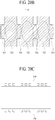
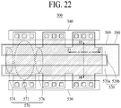
- FIG. 19 illustrates a plan layout of a TFT 500 according to a sixth embodiment of the present invention and is a diagram illustrating a plan layout of a pull-down TFT among a plurality of buffer TFTs included in a scan circuit of a gate driver.
- FIG. 20A is a diagram illustrating a gate electrode in a plan layout of a pull-down TFT illustrated in FIG. 19 .
- FIG. 20B is a diagram illustrating an active layer in the plan layout of the pull-down TFT illustrated in FIG. 19 .
- FIG. 20C is a diagram illustrating a source electrode and a drain electrode in the plan layout of the pull-down TFT illustrated in FIG. 19 .
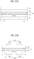
- FIG. 21A is a diagram illustrating a cross-sectional surface taken along line 11-12 of FIG. 19 .
- FIG. 21B is a diagram illustrating a cross-sectional surface taken along line 13-14 of FIG. 19 .
- the TFT 500 according to the sixth embodiment of the present invention may be applied to a plurality of buffer TFTs (a pull-up TFT and a pull-down TFT) of a scan circuit.
- a pull-up TFT and a pull-down TFT a pull-up TFT and a pull-down TFT
- T1 of FIG. 1 a pull-down TFT among the buffer TFTs of the scan circuit
- the pull-down TFT of the scan circuit may be implemented to have a larger area than those of general switching TFTs so as not to be deteriorated by a high voltage and long-time driving.
- a gate electrode 520 may be formed in a double line structure for forming a multichannel.
- a first line 520a and a second line 520b of the gate electrode 520 may be electrically connected to each other.
- An active layer 510 may be disposed to overlap the first line 520a and second line 520b of the gate electrode 520, thereby forming the multichannel.
- the TFT 500 according to the sixth embodiment of the present invention may be formed in a top gate structure.
- the active layer 510 may be formed on an insulator, and a gate insulator 550 may be formed on the active layer 510.
- the gate electrode 520 may be formed on the gate insulator 550.
- the gate electrode 520 may branch as two the lines 520a and 520b from a gate line and may be long formed in a horizontal direction.
- a source electrode 530 may be disposed under the gate electrode 520
- a drain electrode 540 may be disposed on the gate electrode 520.
- the present embodiment is not limited thereto.
- the drain electrode 540 may be disposed under the gate electrode 520
- the source electrode 530 may be disposed on the gate electrode 520.
- the active layer 510 may be formed to overlap the gate electrode 520, and a channel area 512 of the active layer 510 may contact the source electrode 530 and the drain electrode 540.
- the gate electrode 520 may not wholly overlap the active layer 510, and the gate electrode 520 may partially overlap the active layer 510.
- the source electrode 530 and the drain electrode 540 may be respectively disposed at both ends of the active layer 510.
- the source electrode 530 may be connected to a data line through a contact metal which is provided in a contact hole, and the drain electrode 540 may be connected to an anode electrode (or a signal line) of an organic light emitting diode (OLED).
- OLED organic light emitting diode
- the active layer 510 may include a plurality of channel areas 512, a dummy area 514 which is disposed at each of a left edge and a right edge of each of a plurality of the channel areas 512, and a plurality of link areas 516 which are disposed between the plurality of channel areas 512.
- the active layer 510 may be formed of low-temperature poly silicon (LTPS), but is not limited thereto.
- the active layer 510 may be formed of amorphous silicon (a-Si), poly-Si, oxide, an organic material, or the like.
- the plurality of channel areas 512 may overlap the gate electrode 520 for forming a multichannel and may be disposed between the source electrode 530 and the drain electrode 540.
- the plurality of link areas 516 may be respectively disposed between the plurality of channel areas 512 and may connect the plurality of channel areas 512. That is, the plurality of channel areas 512 may be connected in one pattern by the plurality of link areas 516.
- the plurality of channel areas 512 and the plurality of link areas 516 may be formed by patterning a conductive transparent material (for example, indium tin oxide (ITO) or the like) layer. Therefore, the plurality of channel areas 512 and the plurality of link areas 516 may be formed of the same material.
- a conductive transparent material for example, indium tin oxide (ITO) or the like
- a vertical width of each of the plurality of link areas 516 may be formed greater than a vertical-direction width of each of the two lines 520a and 520b of the gate electrode 520.
- a width of each of the plurality of link areas 516 may be formed less than that of the gate electrode 520, but the vertical width of each of the plurality of link areas 516 may be greater than the sum of vertical widths of the first and second lines 520a and 520b of the gate electrode 520.
- a link area is not formed at a portion corresponding to an empty space between two lines of a gate electrode.
- the link area 516 is formed at a portion corresponding to an empty space between the two lines 520a and 520b of the gate electrode 520.
- a display apparatus has a resolution of quad high definition (QHD) or more (for example, a 4K resolution or an 8K resolution), channel lengths of a TFT of a pixel circuit and a buffer TFT of a scan circuit are reduced.
- QHD quad high definition
- the link area 516 may be formed at the portion corresponding to the empty space between the two lines 520a and 520b of the gate electrode 520. Therefore, the channel area 512, the dummy area 514, and the link area 516 for preventing or reducing humps may be applied to high-resolution display apparatuses.
- the link area 516 may be formed at the portion corresponding to the empty space between the two lines 520a and 520b of the gate electrode 520 and thus may connect the plurality of channel areas 512. Therefore, the channel area 512, the dummy area 514, and the link area 516 for preventing or reducing humps may be applied to display apparatuses having a high resolution (QHD, 4K or 8K).
- the dummy area 514 may be disposed at each of a left edge and a right edge of the channel area 512. That is, the dummy area 514 may protrude from each of the left edge and right edge of the channel area 512. For example, the dummy area 514 may protrude by a length corresponding to 10% to 30% of a horizontal width of one the channel area 512.
- a length of the dummy area 514 protruding from the channel area 512 is not limited to 10% to 30% of a horizontal width of one the channel area 512. It is set by the inventors that the dummy area 514 protrudes by a length corresponding to a maximum of 30% of a horizontal width of one the channel area 512 in consideration of the design of a pull-down TFT configuring a scan circuit and a manufacturing process margin.
- the dummy area 514 may protrude by a length corresponding to 10% to 30% of a width of the gate electrode 520.
- the length of the dummy area 514 protruding from the channel area 512 is not limited to 10% to 30% of the width of the gate electrode 520. It is set by the inventors that the dummy area 514 protrudes by a length corresponding to a maximum of 30% of the width of the gate electrode 520 in consideration of the design of the pull-down TFT configuring the scan circuit and the manufacturing process margin.
- the dummy area 514 may protrude by a length corresponding to 10% to 30% of a width of a portion where the gate electrode 520 overlaps the active layer 510.
- the length of the dummy area 514 protruding from the channel area 512 is not limited to 10% to 30% of the width of the portion where the gate electrode 520 overlaps the active layer 510. It is set by the inventors that the dummy area 514 protrudes by a length corresponding to a maximum of 30% of the width of the portion where the gate electrode 520 overlaps the active layer 510, in consideration of the design of the pull-down TFT configuring the scan circuit and the manufacturing process margin.
- the dummy area 514 may protrude by a length corresponding to 50% to 100% of the width of the portion where the gate electrode 520 overlaps the active layer 510.
- the length of the dummy area 514 protruding from the channel area 512 is not limited to 50% to 100% of the width of the portion where the gate electrode 520 overlaps the active layer 510. It is set by the inventors that the dummy area 514 protrudes by a length corresponding to a maximum of 100% of the width of the portion where the gate electrode 520 overlaps the active layer 510, in consideration of the design of the driving TFT configuring the pixel circuit and the manufacturing process margin.
- a parasitic TFT cannot be formed at a left end and a right end of the active layer 510, or the number of parasitic TFTs is minimized.
- a parasitic TFT since the parasitic TFT is disposed in the dummy area 514, a hump is prevented from occurring due to a parasitic TFT which is formed in a buffer TFT of the scan circuit, thereby enhancing an output characteristic of the buffer TFT of the scan circuit. If the output characteristic of the buffer TFT of the scan circuit is enhanced, a screen defect of a display apparatus is prevented, and thus, display quality is enhanced.
- the TFT 500 according to the sixth embodiment of the present invention is applied to the buffer TFTs (in detail, the pull-down TFT) of the scan circuit of the gate driver, a leakage current (or an off current) is prevented from occurring in the scan circuit or is reduced. Accordingly, a signal is normally output through the Q node and QB node of the scan circuit, and thus, a screen defect of a display apparatus is prevented.
- FIG. 22 illustrates a plan layout of a TFT according to a seventh embodiment of the present invention and is a plan view illustrating a pull-down TFT of a scan circuit formed in a double gate structure and a plurality of channels formed in an active layer.
- FIG. 23A is a cross-sectional view of a pull-down TFT of a scan circuit taken along line J1-J2 of FIG. 22 .
- FIG. 23B is a cross-sectional view of the pull-down TFT of the scan circuit taken along line J3-J4 of FIG. 22 .
- a pull-down TFT 500 may be formed in a double gate structure where an upper gate electrode 560 is disposed on an active layer 570 and a lower gate electrode 580 is disposed under the active layer 570.
- the pull-down TFT 500 of the scan circuit may be implemented to have a larger area than those of general switching TFTs so as not to be deteriorated by a high voltage and long-time driving.
- the active layer 570 may be disposed on an insulator, and a gate insulator 550 may be disposed on the active layer 570.
- the upper gate electrode 560 (a first gate electrode) may be disposed on the gate insulator 550.
- the lower gate electrode 580 (a second gate electrode) may be disposed under the insulator.
- the upper gate electrode 560 may be electrically connected to the lower gate electrode 580 through a contact.
- Two lines 560a and 560b of the upper gate electrode 560 may be electrically connected to each other.
- a first line 560a and a second line 560b of the upper gate electrode 560 may be electrically connected to each other, and an active layer 570 may be disposed in order for the first line 560a and second line 560b of the upper gate electrode 560 to overlap each other, thereby forming a multichannel.
- two lines 580a and 580b of the lower gate electrode 580 may be electrically connected to each other.
- a first line 580a and a second line 580b of the lower gate electrode 580 may be electrically connected to each other, and the active layer 570 may be disposed in order for the first line 580a and second line 580b of the lower gate electrode 580 to overlap each other, thereby forming a multichannel.
- the upper gate electrode 560 and the lower gate electrode 580 may be formed in the same shape and may be disposed with the active layer 570 therebetween. In this case, an interval between an edge of the upper gate electrode 560 and an end of a dummy area 574 may be the same as an interval between an edge of the lower gate electrode 580 and the end of the dummy area 574.
- the present embodiment is not limited thereto.
- the upper gate electrode 560 and the lower gate electrode 580 may be formed in different shapes.
- the end of the dummy area 574 may be separated from an end of the upper gate electrode 560 by a first interval, and the end of the dummy area 574 may be separated from an end of the lower gate electrode 580 by a second interval. That is, the interval between the edge of the upper gate electrode 560 and the end of the dummy area 574 may differ from the interval between the edge of the lower gate electrode 580 and the end of the dummy area 574.
- the active layer 570 may include a plurality of channel areas 572 and a plurality of link areas 576 which are disposed between the plurality of channel areas 572.
- the active layer 570 may be formed of low-temperature poly silicon (LTPS), but is not limited thereto.
- the active layer 570 may be formed of amorphous silicon (a-Si), poly-Si, oxide, an organic material, or the like.
- the plurality of channel areas 572 may be disposed between the upper gate electrode 560 and the lower gate electrode 580.
- the plurality of link areas 576 may be respectively disposed between the plurality of channel areas 572 and may connect a plurality of channel areas 572. That is, the plurality of channel areas 572 may be connected in one pattern by the plurality of link areas 576.
- the plurality of channel areas 572, the plurality of dummy areas 574, and the plurality of link areas 576 may be formed by patterning a conductive transparent material (for example, indium tin oxide (ITO) or the like) layer. Therefore, the plurality of channel areas 572, the plurality of dummy areas 574, and the plurality of link areas 576 may be formed of the same material.
- a conductive transparent material for example, indium tin oxide (ITO) or the like
- the upper gate electrode 560 may be disposed on the active layer 570 to overlap the active layer 570, and thus, a first channel 570a may be formed on a top of the active layer 570.
- the lower gate electrode 580 may be disposed under the active layer 570 to overlap the active layer 570, and thus, a second channel 570b may be formed on a bottom of the active layer 570. That is, if a pull-down TFT of a scan circuit is formed in a double gate structure, a channel may be formed on each of the top and bottom of the active layer 570, and thus, the active layer 570 may include a plurality of channels 570a and 570b.
- the double gate structure may be applied to a switching TFT (a reset TFT) of the scan circuit, a switching TFT of a pixel circuit, and a driving TFT of the pixel circuit. Therefore, even in the switching TFT (the reset TFT) of the scan circuit, the switching TFT of the pixel circuit, and the driving TFT of the pixel circuit, a channel may be formed on each of a top and a bottom of an active layer.
- a switching TFT a reset TFT
- a TFT having the double gate structure is two times the number of channels, namely, two times a width of a channel, and thus, an output characteristic of the TFT is enhanced.
- FIG. 24 is a diagram showing effects where, by changing a pattern of an active layer of a pull-down TFT according to a seventh embodiment of the present invention, an output characteristic of the pull-down TFT is enhanced, and humps are reduced.
- a hump is prevented from occurring in a pull-down TFT of a scan circuit.
- a flatband voltage Vfb and a threshold voltage Vth of a TFT may increase.
- an on current Ion may be enhanced.
- an output characteristic curve of a TFT is shown.
- the output characteristic curve may consist of a 1 region, which shows a low current output characteristic, and a 2 region that shows a high current output characteristic.
- an output characteristic curve (a) may be shifted (shifted to the left) in a direction of a low voltage in the 1 region, and in the 2 region, an output characteristic curve (b) may be shifted (shifted to the right) in a direction of a high voltage.
- a switching TFT (a reset TFT) of the scan circuit, a switching TFT of a pixel circuit, and a driving TFT of the pixel circuit, by changing a pattern of an active layer, a hump cannot occur in the TFTs.
- the pull-down TFT of the scan circuit normally outputs a signal, thereby enhancing the display quality of a display apparatus.
- a vertical width of each of the plurality of link areas may be less than that of each of the plurality of lines.
- each of the plurality of link areas may be greater than that of each of the plurality of lines.
- each of the plurality of link areas may be greater than the sum of vertical widths of the plurality of lines.
- each of the plurality of link areas may include a slit, and the slit may be disposed to overlap a portion corresponding to a space between the plurality of lines.
- the plurality of link areas may be disposed to overlap a portion corresponding to the space between the plurality of lines.
- the dummy area may protrude from one edge or both edges of the channel area and may be disposed at an outer portion of the first gate electrode.
- the dummy area may protrude to the outer portion of the first gate electrode by a length corresponding to a maximum of 30% of a width of the first gate electrode.
- the dummy area may protrude to the outer portion of the first gate electrode by a length corresponding to a maximum of 30% of a width of a portion where the first gate electrode overlaps the active layer.
- the dummy area may protrude to the outer portion of the first gate electrode by a length corresponding to a maximum of 100% of the width of the portion where the first gate electrode overlaps the active layer.
- the dummy area may protrude from one edge or both edges of the channel area and protrude by a length corresponding to a maximum of 30% of a horizontal width of one channel area.
- a first threshold voltage of the dummy area may be higher than a second threshold voltage of the channel area.
- the above-described TFT of the display apparatus may include: an insulator disposed under an active layer; and a second gate electrode disposed under the insulator, the second gate electrode branching as a plurality of lines.
- the second gate electrode may be disposed to overlap the active layer, and the first gate electrode may be electrically connected to the second gate electrode.
- the active layer may overlap a plurality of lines of the first gate electrode to thereby form a multichannel on a top of the active layer.
- the active layer may overlap the plurality of lines of the second gate electrode to thereby form a multichannel on a bottom of the active layer.
- an end of each of the plurality of channel areas may not overlap the first gate electrode.
- each of the plurality of channel areas may not overlap the second gate electrode.
- the TFT prevents a hump from occurring, thereby reducing a leakage current.
- the occurrence of a hump is prevented by changing the active layer pattern of the TFT included in the scan circuit of the gate driver, and thus, the output voltage Vgout of the scan circuit is prevented from being dropped, thereby preventing a screen defect of the display apparatus.
- a leakage current (or an off current) is prevented from occurring due to a hump, thereby preventing a screen defect of the display apparatus.
Landscapes
- Engineering & Computer Science (AREA)
- Power Engineering (AREA)
- Microelectronics & Electronic Packaging (AREA)
- Physics & Mathematics (AREA)
- Condensed Matter Physics & Semiconductors (AREA)
- General Physics & Mathematics (AREA)
- Computer Hardware Design (AREA)
- Ceramic Engineering (AREA)
- Devices For Indicating Variable Information By Combining Individual Elements (AREA)
- Electroluminescent Light Sources (AREA)
Claims (11)
- Ein Dünnfilmtransistor (TFT) für eine Anzeigevorrichtung, wobei der TFT (100; 500) aufweist:eine aktive Schicht (110; 510; 570), die auf einem Substrat angeordnet ist;eine erste Gate-Elektrode (120; 520; 560), die an einer Seite der aktiven Schicht, welche der dem Substrat zugewandten Seite gegenüberliegt, angeordnet ist, sodass sie die aktive Schicht überlappt, wobei die erste Gate-Elektrode eine Mehrzahl von Leitungen (520a, 520b; 560a, 560b) aufweist;einen Gate-Isolator (150; 550), der zwischen der aktiven Schicht und der ersten Gate-Elektrode und über Abschnitten der aktiven Schicht (110; 510; 570), die die erste Gate-Elektrode (120; 520; 560) nicht überlappen, angeordnet ist; undeine Source-Elektrode (130; 530) und eine Drain-Elektrode (140; 540), die an beiden Enden der aktiven Schicht und parallel zu einer Richtung der Mehrzahl von Leitungen der ersten Gate-Elektrode (120; 520; 560) angeordnet sind,wobei eine Mehrzahl von Gruppen elektrischer Kontakte zwischen der aktiven Schicht (110; 510; 570) und der Source-Elektrode (130; 530), beziehungsweise zwischen der aktiven Schicht (110; 510; 570) und der Drain-Elektrode (140; 540) angeordnet sind, sodass zwischen den Gruppen elektrischer Kontakte Bereiche angeordnet sind, welche frei von Kontakten sind,wobei die aktive Schicht (110; 510; 570) aufweist:eine Mehrzahl von Kanalbereichen (112; 512; 572), die zwischen der Source-Elektrode (130; 530) und der Drain-Elektrode (140; 540) in Bereichen angeordnet sind, in denen die elektrischen Kontakte zu der aktiven Schicht (110; 510; 570) gebildet sind;einen oder mehrere Dummy-Bereiche (114; 514; 574), wobei sich eine Länge von jedem des einen oder der mehreren Dummy-Bereiche von einem Rand eines korrespondierenden Kanalbereichs (112; 512; 572) zu einer Seite erstreckt, auf der kein angrenzender Kanalbereich (112; 512; 572) angeordnet ist; undeine Mehrzahl von Verbindungsbereichen (116; 516; 576), die zwischen der Mehrzahl von Kanalbereichen (112; 512; 572) angeordnet sind, um die Mehrzahl von Kanalbereichen in einer Struktur zu verbinden, dadurch gekennzeichnet, dasssich die aktive Schicht (110; 510; 570) über die erste Gate-Elektrode (120; 520; 560) in der Richtung der Mehrzahl von Leitungen der ersten Gate-Elektrode (120; 520; 560) erstreckt.
- Der TFT (100) gemäß Anspruch 1, wobei eine Breite von jedem der Mehrzahl von Verbindungsbereichen (116) in einer Richtung, die senkrecht zu der Richtung der Mehrzahl von Leitungen der ersten Gate-Elektrode ist, geringer ist als eine Breite von jeder der Mehrzahl von Leitungen der ersten Gate-Elektrode.
- Der TFT (100) gemäß Anspruch 1, wobei eine Breite von jedem der Mehrzahl von Verbindungsbereichen (116) in einer Richtung, die senkrecht zu der Richtung der Mehrzahl von Leitungen der ersten Gate-Elektrode ist, größer ist als eine Breite von jeder der Mehrzahl von Leitungen der ersten Gate-Elektrode.
- Der TFT (100) gemäß Anspruch 1 oder 3, wobei eine Breite von jedem der Mehrzahl von Verbindungsbereichen (116) in einer Richtung, die senkrecht zu der Richtung der Mehrzahl von Leitungen der ersten Gate-Elektrode ist, größer ist als eine Summe von Breiten der Mehrzahl von Leitungen der ersten Gate-Elektrode.
- Der TFT (100) gemäß irgendeinem der Ansprüche 1 bis 4, wobei eine Mehrzahl von Schlitzen zwischen angrenzenden Kanalbereichen (112; 512; 572) angeordnet sind, sodass sie einen Abschnitt überlappen, der mit einem Raum zwischen der Mehrzahl von Leitungen der ersten Gate-Elektrode korrespondiert, sodass der jeweilige Verbindungsbereich (116) so angeordnet ist, dass er die Mehrzahl von Leitungen der ersten Gate-Elektrode überlappt.
- Der TFT (500) gemäß irgendeinem der Ansprüche 1 bis 4, wobei die Mehrzahl von Verbindungsbereichen (516; 576) so angeordnet sind, dass sie einen Bereich überlappen, der mit einem Raum zwischen der Mehrzahl von Leitungen (520a, 520b) korrespondiert,
wobei die Mehrzahl von Leitungen der ersten Gate-Elektrode parallel zueinander sind. - Der TFT (500) gemäß irgendeinem der Ansprüche 1 bis 6, wobei jeder des einen oder der mehreren Dummy-Bereiche (514) von einem Rand oder von beiden Rändern eines korrespondierenden Kanalbereichs (512) vorsteht und an einem Endbereich der Mehrzahl von Leitungen der ersten Gate-Elektrode (520) angeordnet ist.
- Der TFT (500) gemäß Anspruch 7, wobei jeder des einen oder der mehreren Dummy-Bereiche (514) von dem Endabschnitt der ersten Gate-Elektrode (520) um eine Länge vorsteht, die einem Maximum von 30% einer Länge der Leitungen der ersten Gate-Elektrode (520) entspricht.
- Der TFT (500) gemäß Anspruch 7, wobei jeder des einen oder der mehreren Dummy-Bereiche (514) von dem einen Rand oder von den beiden Rändern des korrespondierenden Kanalbereichs (512) um eine Länge vorsteht, die einem Maximum von 30% einer Breite des einen Kanalbereichs (512) in der Richtung der Mehrzahl von Leitungen der ersten Gate-Elektrode entspricht.
- Der TFT (500) gemäß irgendeinem der Ansprüche 1 bis 9, ferner aufweisend:einen Isolator, der unter der aktiven Schicht (570) angeordnet ist; undeine zweite Gate-Elektrode (580), die unter dem Isolator angeordnet ist, wobei die zweite Gate-Elektrode (580) eine Mehrzahl von Leitungen aufweist, welche die gleiche Form haben wie die Mehrzahl von Leitungen der ersten Gate-Elektrode (580a, 580b),wobei die zweite Gate-Elektrode (580) so angeordnet ist, dass sie die aktive Schicht (570) überlappt, und wobei die erste Gate-Elektrode (560) elektrisch mit der zweiten Gate-Elektrode (580) verbunden ist,wobei vorzugsweise:
die aktive Schicht (570) die Mehrzahl von Leitungen (560a, 560b) der ersten Gate-Elektrode (560) überlappt, um dadurch einen Mehrfachkanal an einer Oberseite der aktiven Schicht (570) zu bilden, und die aktive Schicht (570) die Mehrzahl von Leitungen (580a, 580b) der zweiten Gate-Elektrode (580) überlappt, um dadurch einen Mehrfachkanal an einer Unterseite der aktiven Schicht (570) zu bilden. - Einen Dünnfilmtransistor (TFT) für eine Anzeigevorrichtung, wobei der TFT (200; 300) aufweist:eine aktive Schicht (210, 310), die auf einem Substrat angeordnet ist;eine erste Gate-Elektrode (220; 320), die so an einer Seite der aktiven Schicht, welche der dem Substrat zugewandten Seite gegenüberliegt, angeordnet ist, dass sie die aktive Schicht teilweise überlappt, wobei die erste Gate-Elektrode eine Mehrzahl von Leitungen aufweist;einen Gate-Isolator (250; 350), der zwischen der aktiven Schicht und der ersten Gate-Elektrode und über Abschnitten der aktiven Schicht (210; 310), die die erste Gate-Elektrode (220; 320) nicht überlappen, angeordnet ist; undeine Source-Elektrode (230; 330) und eine Drain-Elektrode (240; 340), die an beiden Enden der aktiven Schicht und parallel zu einer Richtung der Mehrzahl von Leitungen der ersten Gate-Elektrode (220; 320) angeordnet sind,wobei eine Mehrzahl elektrischer Kontakte zwischen der aktiven Schicht (210; 310) und der Source-Elektrode (230; 330), beziehungsweise der aktiven Schicht (110; 510; 570) und der Drain-Elektrode (240; 340) angeordnet sind, sodass neben der Mehrzahl von elektrischen Kontakten Bereiche angeordnet sind, welche frei von Kontakten sind,wobei die aktive Schicht (210; 310) aufweist:einen Kanalbereich (212; 314), der zwischen der Source-Elektrode (230; 330) und der Drain-Elektrode (240; 340) in einem Bereich angeordnet ist, in dem die Mehrzahl von elektrischen Kontakten zu der aktiven Schicht (210; 310) angeordnet sind;einen oder mehrere Dummy-Bereiche (214; 314), wobei sich eine Länge von jedem des einen oder der mehreren Dummy-Bereiche von einem Rand des korrespondierenden Kanalbereichs (212; 314) erstreckt, dadurch gekennzeichnet, dasssich die aktive Schicht (210; 310) über die erste Gate-Elektrode (220; 320) in der Richtung der Mehrzahl von Leitungen der ersten Gate-Elektrode (220; 320) erstreckt.
Applications Claiming Priority (3)
| Application Number | Priority Date | Filing Date | Title |
|---|---|---|---|
| KR20140080195 | 2014-06-27 | ||
| KR1020150083192A KR102395635B1 (ko) | 2014-06-27 | 2015-06-12 | 디스플레이 장치의 박막트랜지스터 |
| KR1020150083189A KR102377151B1 (ko) | 2014-06-27 | 2015-06-12 | 디스플레이 장치의 박막트랜지스터 |
Publications (2)
| Publication Number | Publication Date |
|---|---|
| EP2960943A1 EP2960943A1 (de) | 2015-12-30 |
| EP2960943B1 true EP2960943B1 (de) | 2019-08-07 |
Family
ID=53476778
Family Applications (1)
| Application Number | Title | Priority Date | Filing Date |
|---|---|---|---|
| EP15173323.5A Active EP2960943B1 (de) | 2014-06-27 | 2015-06-23 | Dünnfilmtransistor für eine anzeigevorrichtung |
Country Status (3)
| Country | Link |
|---|---|
| US (1) | US9450106B2 (de) |
| EP (1) | EP2960943B1 (de) |
| CN (1) | CN105226100B (de) |
Families Citing this family (14)
| Publication number | Priority date | Publication date | Assignee | Title |
|---|---|---|---|---|
| BR112017023119B1 (pt) * | 2016-07-08 | 2022-11-16 | Chongqing Boe Optoelectronics Technology Co., Ltd. | Transistor de película fina, circuito de acionamento de gate em matriz, aparelho de exibição e método de fabricação |
| US10157572B2 (en) * | 2016-11-01 | 2018-12-18 | Innolux Corporation | Pixel driver circuitry for a display device |
| CN106783888B (zh) * | 2017-01-03 | 2020-06-30 | 京东方科技集团股份有限公司 | 显示屏及其控制方法、显示装置 |
| CN106997904B (zh) * | 2017-04-17 | 2020-01-07 | 京东方科技集团股份有限公司 | 薄膜晶体管及制备方法、栅极驱动电路 |
| KR102420080B1 (ko) * | 2017-05-19 | 2022-07-13 | 삼성디스플레이 주식회사 | 다채널 박막 트랜지스터 및 이를 포함하는 화소 |
| CN106991979B (zh) * | 2017-05-25 | 2019-06-07 | 上海天马微电子有限公司 | 一种电子纸及显示装置 |
| CN109256418A (zh) * | 2017-07-14 | 2019-01-22 | 京东方科技集团股份有限公司 | 薄膜晶体管及其制备方法、阵列基板和显示装置 |
| CN109509793B (zh) * | 2017-09-15 | 2020-12-01 | 京东方科技集团股份有限公司 | 薄膜晶体管、其制造方法及电子装置 |
| KR102467465B1 (ko) * | 2018-01-04 | 2022-11-16 | 삼성디스플레이 주식회사 | 수직 적층 트랜지스터, 이를 포함하는 표시 장치, 및 그 제조 방법 |
| KR102653121B1 (ko) * | 2018-07-25 | 2024-04-02 | 삼성디스플레이 주식회사 | 유기 발광 표시 장치 |
| CN110109306B (zh) * | 2019-04-25 | 2020-12-08 | 武汉华星光电技术有限公司 | 阵列基板及其制造方法、显示面板 |
| CN110289309B (zh) * | 2019-06-10 | 2021-04-27 | Tcl华星光电技术有限公司 | 薄膜晶体管及电路 |
| CN111048524A (zh) * | 2019-11-26 | 2020-04-21 | 深圳市华星光电半导体显示技术有限公司 | 阵列基板及制备方法、显示面板 |
| US20230082769A1 (en) * | 2020-03-30 | 2023-03-16 | Sharp Kabushiki Kaisha | Display device and method for manufacturing display device |
Family Cites Families (11)
| Publication number | Priority date | Publication date | Assignee | Title |
|---|---|---|---|---|
| US3649888A (en) * | 1969-05-14 | 1972-03-14 | Itt | Dielectric structure for semiconductor device |
| JP3256110B2 (ja) * | 1995-09-28 | 2002-02-12 | シャープ株式会社 | 液晶表示装置 |
| CN100502047C (zh) * | 1996-06-28 | 2009-06-17 | 精工爱普生株式会社 | 薄膜晶体管 |
| JP3702096B2 (ja) * | 1998-06-08 | 2005-10-05 | 三洋電機株式会社 | 薄膜トランジスタ及び表示装置 |
| KR101022559B1 (ko) * | 2003-12-30 | 2011-03-16 | 엘지디스플레이 주식회사 | 액정 표시 장치 및 그 제조 방법 |
| KR100603832B1 (ko) * | 2004-05-03 | 2006-07-24 | 엘지.필립스 엘시디 주식회사 | 열분산형 멀티채널 트랜지스터와 그 제조방법 |
| JP2006128160A (ja) * | 2004-10-26 | 2006-05-18 | Seiko Epson Corp | 半導体装置及びその製造方法 |
| GB2459666A (en) * | 2008-04-29 | 2009-11-04 | Sharp Kk | Thin film transistor with low leakage current |
| US7767546B1 (en) * | 2009-01-12 | 2010-08-03 | International Business Machines Corporation | Low cost fabrication of double box back gate silicon-on-insulator wafers with built-in shallow trench isolation in back gate layer |
| US8946066B2 (en) * | 2011-05-11 | 2015-02-03 | Semiconductor Energy Laboratory Co., Ltd. | Method of manufacturing semiconductor device |
| JP6110693B2 (ja) * | 2012-03-14 | 2017-04-05 | 株式会社半導体エネルギー研究所 | 半導体装置 |
-
2015
- 2015-06-23 EP EP15173323.5A patent/EP2960943B1/de active Active
- 2015-06-25 US US14/750,217 patent/US9450106B2/en active Active
- 2015-06-26 CN CN201510364330.3A patent/CN105226100B/zh active Active
Non-Patent Citations (1)
| Title |
|---|
| None * |
Also Published As
| Publication number | Publication date |
|---|---|
| EP2960943A1 (de) | 2015-12-30 |
| US9450106B2 (en) | 2016-09-20 |
| CN105226100B (zh) | 2018-06-26 |
| CN105226100A (zh) | 2016-01-06 |
| US20150380567A1 (en) | 2015-12-31 |
Similar Documents
| Publication | Publication Date | Title |
|---|---|---|
| EP2960943B1 (de) | Dünnfilmtransistor für eine anzeigevorrichtung | |
| US10453387B2 (en) | Display panel, display device, pixel driving circuit, and control method for the same | |
| US10923506B2 (en) | Electroluminescence display device | |
| KR102071301B1 (ko) | 유기 전계 발광 표시 장치 | |
| US11476284B2 (en) | Display device | |
| US20140240521A1 (en) | Organic light emitting display panel | |
| KR20200064230A (ko) | 유기 발광 표시 장치 | |
| KR20160096787A (ko) | 유기 발광 표시 장치 | |
| KR102693264B1 (ko) | 화소 및 이를 구비한 표시 장치 | |
| US20210193036A1 (en) | Pixel unit, array substrate and display terminal | |
| US9291870B2 (en) | Thin film transistor and display device having the same | |
| KR100814854B1 (ko) | 유기전계발광표시장치 및 그 구동방법 | |
| KR20160030628A (ko) | 유기 발광 다이오드 표시 장치 | |
| EP3859784A1 (de) | Arraysubstrat und verfahren zur herstellung davon sowie anzeigetafel | |
| KR20200076302A (ko) | 표시 패널 및 표시 장치 | |
| CN105448243A (zh) | 像素电路及其驱动方法以及显示装置 | |
| US10621912B2 (en) | Display device to display images on rear and front surfaces independently of each other | |
| KR100560452B1 (ko) | 발광 표시 패널 및 발광 표시 장치 | |
| KR20170081036A (ko) | 유기발광표시패널 및 유기발광표시장치 | |
| WO2020177258A1 (zh) | 像素驱动电路及显示面板 | |
| KR20190074812A (ko) | 구동 박막트랜지스터 및 이를 포함하는 유기발광표시장치 | |
| KR102480109B1 (ko) | 유기발광표시패널 및 유기발광표시장치 | |
| KR101550837B1 (ko) | 유기전계 발광소자 | |
| KR20190078180A (ko) | 박막트랜지스터 및 그를 포함하는 유기발광표시장치 | |
| KR102377151B1 (ko) | 디스플레이 장치의 박막트랜지스터 |
Legal Events
| Date | Code | Title | Description |
|---|---|---|---|
| PUAI | Public reference made under article 153(3) epc to a published international application that has entered the european phase |
Free format text: ORIGINAL CODE: 0009012 |
|
| 17P | Request for examination filed |
Effective date: 20150623 |
|
| AK | Designated contracting states |
Kind code of ref document: A1 Designated state(s): AL AT BE BG CH CY CZ DE DK EE ES FI FR GB GR HR HU IE IS IT LI LT LU LV MC MK MT NL NO PL PT RO RS SE SI SK SM TR |
|
| AX | Request for extension of the european patent |
Extension state: BA ME |
|
| RBV | Designated contracting states (corrected) |
Designated state(s): AL AT BE BG CH CY CZ DE DK EE ES FI FR GB GR HR HU IE IS IT LI LT LU LV MC MK MT NL NO PL PT RO RS SE SI SK SM TR |
|
| STAA | Information on the status of an ep patent application or granted ep patent |
Free format text: STATUS: REQUEST FOR EXAMINATION WAS MADE |
|
| R17P | Request for examination filed (corrected) |
Effective date: 20150623 |
|
| REG | Reference to a national code |
Ref country code: DE Ref legal event code: R079 Ref document number: 602015035127 Country of ref document: DE Free format text: PREVIOUS MAIN CLASS: H01L0029786000 Ipc: H01L0029423000 |
|
| GRAP | Despatch of communication of intention to grant a patent |
Free format text: ORIGINAL CODE: EPIDOSNIGR1 |
|
| STAA | Information on the status of an ep patent application or granted ep patent |
Free format text: STATUS: GRANT OF PATENT IS INTENDED |
|
| RIC1 | Information provided on ipc code assigned before grant |
Ipc: H01L 29/423 20060101AFI20190110BHEP Ipc: H01L 29/06 20060101ALI20190110BHEP Ipc: H01L 29/786 20060101ALI20190110BHEP |
|
| INTG | Intention to grant announced |
Effective date: 20190128 |
|
| GRAS | Grant fee paid |
Free format text: ORIGINAL CODE: EPIDOSNIGR3 |
|
| GRAA | (expected) grant |
Free format text: ORIGINAL CODE: 0009210 |
|
| STAA | Information on the status of an ep patent application or granted ep patent |
Free format text: STATUS: THE PATENT HAS BEEN GRANTED |
|
| AK | Designated contracting states |
Kind code of ref document: B1 Designated state(s): AL AT BE BG CH CY CZ DE DK EE ES FI FR GB GR HR HU IE IS IT LI LT LU LV MC MK MT NL NO PL PT RO RS SE SI SK SM TR |
|
| REG | Reference to a national code |
Ref country code: GB Ref legal event code: FG4D |
|
| REG | Reference to a national code |
Ref country code: CH Ref legal event code: EP Ref country code: AT Ref legal event code: REF Ref document number: 1165154 Country of ref document: AT Kind code of ref document: T Effective date: 20190815 |
|
| REG | Reference to a national code |
Ref country code: DE Ref legal event code: R096 Ref document number: 602015035127 Country of ref document: DE |
|
| REG | Reference to a national code |
Ref country code: IE Ref legal event code: FG4D |
|
| REG | Reference to a national code |
Ref country code: NL Ref legal event code: MP Effective date: 20190807 |
|
| REG | Reference to a national code |
Ref country code: LT Ref legal event code: MG4D |
|
| PG25 | Lapsed in a contracting state [announced via postgrant information from national office to epo] |
Ref country code: LT Free format text: LAPSE BECAUSE OF FAILURE TO SUBMIT A TRANSLATION OF THE DESCRIPTION OR TO PAY THE FEE WITHIN THE PRESCRIBED TIME-LIMIT Effective date: 20190807 Ref country code: FI Free format text: LAPSE BECAUSE OF FAILURE TO SUBMIT A TRANSLATION OF THE DESCRIPTION OR TO PAY THE FEE WITHIN THE PRESCRIBED TIME-LIMIT Effective date: 20190807 Ref country code: NL Free format text: LAPSE BECAUSE OF FAILURE TO SUBMIT A TRANSLATION OF THE DESCRIPTION OR TO PAY THE FEE WITHIN THE PRESCRIBED TIME-LIMIT Effective date: 20190807 Ref country code: SE Free format text: LAPSE BECAUSE OF FAILURE TO SUBMIT A TRANSLATION OF THE DESCRIPTION OR TO PAY THE FEE WITHIN THE PRESCRIBED TIME-LIMIT Effective date: 20190807 Ref country code: HR Free format text: LAPSE BECAUSE OF FAILURE TO SUBMIT A TRANSLATION OF THE DESCRIPTION OR TO PAY THE FEE WITHIN THE PRESCRIBED TIME-LIMIT Effective date: 20190807 Ref country code: PT Free format text: LAPSE BECAUSE OF FAILURE TO SUBMIT A TRANSLATION OF THE DESCRIPTION OR TO PAY THE FEE WITHIN THE PRESCRIBED TIME-LIMIT Effective date: 20191209 Ref country code: BG Free format text: LAPSE BECAUSE OF FAILURE TO SUBMIT A TRANSLATION OF THE DESCRIPTION OR TO PAY THE FEE WITHIN THE PRESCRIBED TIME-LIMIT Effective date: 20191107 Ref country code: NO Free format text: LAPSE BECAUSE OF FAILURE TO SUBMIT A TRANSLATION OF THE DESCRIPTION OR TO PAY THE FEE WITHIN THE PRESCRIBED TIME-LIMIT Effective date: 20191107 |
|
| REG | Reference to a national code |
Ref country code: AT Ref legal event code: MK05 Ref document number: 1165154 Country of ref document: AT Kind code of ref document: T Effective date: 20190807 |
|
| PG25 | Lapsed in a contracting state [announced via postgrant information from national office to epo] |
Ref country code: IS Free format text: LAPSE BECAUSE OF FAILURE TO SUBMIT A TRANSLATION OF THE DESCRIPTION OR TO PAY THE FEE WITHIN THE PRESCRIBED TIME-LIMIT Effective date: 20191207 Ref country code: ES Free format text: LAPSE BECAUSE OF FAILURE TO SUBMIT A TRANSLATION OF THE DESCRIPTION OR TO PAY THE FEE WITHIN THE PRESCRIBED TIME-LIMIT Effective date: 20190807 Ref country code: AL Free format text: LAPSE BECAUSE OF FAILURE TO SUBMIT A TRANSLATION OF THE DESCRIPTION OR TO PAY THE FEE WITHIN THE PRESCRIBED TIME-LIMIT Effective date: 20190807 Ref country code: GR Free format text: LAPSE BECAUSE OF FAILURE TO SUBMIT A TRANSLATION OF THE DESCRIPTION OR TO PAY THE FEE WITHIN THE PRESCRIBED TIME-LIMIT Effective date: 20191108 Ref country code: LV Free format text: LAPSE BECAUSE OF FAILURE TO SUBMIT A TRANSLATION OF THE DESCRIPTION OR TO PAY THE FEE WITHIN THE PRESCRIBED TIME-LIMIT Effective date: 20190807 Ref country code: RS Free format text: LAPSE BECAUSE OF FAILURE TO SUBMIT A TRANSLATION OF THE DESCRIPTION OR TO PAY THE FEE WITHIN THE PRESCRIBED TIME-LIMIT Effective date: 20190807 |
|
| PG25 | Lapsed in a contracting state [announced via postgrant information from national office to epo] |
Ref country code: TR Free format text: LAPSE BECAUSE OF FAILURE TO SUBMIT A TRANSLATION OF THE DESCRIPTION OR TO PAY THE FEE WITHIN THE PRESCRIBED TIME-LIMIT Effective date: 20190807 |
|
| PG25 | Lapsed in a contracting state [announced via postgrant information from national office to epo] |
Ref country code: PL Free format text: LAPSE BECAUSE OF FAILURE TO SUBMIT A TRANSLATION OF THE DESCRIPTION OR TO PAY THE FEE WITHIN THE PRESCRIBED TIME-LIMIT Effective date: 20190807 Ref country code: EE Free format text: LAPSE BECAUSE OF FAILURE TO SUBMIT A TRANSLATION OF THE DESCRIPTION OR TO PAY THE FEE WITHIN THE PRESCRIBED TIME-LIMIT Effective date: 20190807 Ref country code: AT Free format text: LAPSE BECAUSE OF FAILURE TO SUBMIT A TRANSLATION OF THE DESCRIPTION OR TO PAY THE FEE WITHIN THE PRESCRIBED TIME-LIMIT Effective date: 20190807 Ref country code: DK Free format text: LAPSE BECAUSE OF FAILURE TO SUBMIT A TRANSLATION OF THE DESCRIPTION OR TO PAY THE FEE WITHIN THE PRESCRIBED TIME-LIMIT Effective date: 20190807 Ref country code: RO Free format text: LAPSE BECAUSE OF FAILURE TO SUBMIT A TRANSLATION OF THE DESCRIPTION OR TO PAY THE FEE WITHIN THE PRESCRIBED TIME-LIMIT Effective date: 20190807 Ref country code: IT Free format text: LAPSE BECAUSE OF FAILURE TO SUBMIT A TRANSLATION OF THE DESCRIPTION OR TO PAY THE FEE WITHIN THE PRESCRIBED TIME-LIMIT Effective date: 20190807 |
|
| PG25 | Lapsed in a contracting state [announced via postgrant information from national office to epo] |
Ref country code: IS Free format text: LAPSE BECAUSE OF FAILURE TO SUBMIT A TRANSLATION OF THE DESCRIPTION OR TO PAY THE FEE WITHIN THE PRESCRIBED TIME-LIMIT Effective date: 20200224 Ref country code: SM Free format text: LAPSE BECAUSE OF FAILURE TO SUBMIT A TRANSLATION OF THE DESCRIPTION OR TO PAY THE FEE WITHIN THE PRESCRIBED TIME-LIMIT Effective date: 20190807 Ref country code: SK Free format text: LAPSE BECAUSE OF FAILURE TO SUBMIT A TRANSLATION OF THE DESCRIPTION OR TO PAY THE FEE WITHIN THE PRESCRIBED TIME-LIMIT Effective date: 20190807 Ref country code: CZ Free format text: LAPSE BECAUSE OF FAILURE TO SUBMIT A TRANSLATION OF THE DESCRIPTION OR TO PAY THE FEE WITHIN THE PRESCRIBED TIME-LIMIT Effective date: 20190807 |
|
| REG | Reference to a national code |
Ref country code: DE Ref legal event code: R097 Ref document number: 602015035127 Country of ref document: DE |
|
| PLBE | No opposition filed within time limit |
Free format text: ORIGINAL CODE: 0009261 |
|
| STAA | Information on the status of an ep patent application or granted ep patent |
Free format text: STATUS: NO OPPOSITION FILED WITHIN TIME LIMIT |
|
| PG2D | Information on lapse in contracting state deleted |
Ref country code: IS |
|
| 26N | No opposition filed |
Effective date: 20200603 |
|
| PG25 | Lapsed in a contracting state [announced via postgrant information from national office to epo] |
Ref country code: SI Free format text: LAPSE BECAUSE OF FAILURE TO SUBMIT A TRANSLATION OF THE DESCRIPTION OR TO PAY THE FEE WITHIN THE PRESCRIBED TIME-LIMIT Effective date: 20190807 |
|
| PG25 | Lapsed in a contracting state [announced via postgrant information from national office to epo] |
Ref country code: MC Free format text: LAPSE BECAUSE OF FAILURE TO SUBMIT A TRANSLATION OF THE DESCRIPTION OR TO PAY THE FEE WITHIN THE PRESCRIBED TIME-LIMIT Effective date: 20190807 |
|
| REG | Reference to a national code |
Ref country code: CH Ref legal event code: PL |
|
| PG25 | Lapsed in a contracting state [announced via postgrant information from national office to epo] |
Ref country code: LU Free format text: LAPSE BECAUSE OF NON-PAYMENT OF DUE FEES Effective date: 20200623 |
|
| REG | Reference to a national code |
Ref country code: BE Ref legal event code: MM Effective date: 20200630 |
|
| PG25 | Lapsed in a contracting state [announced via postgrant information from national office to epo] |
Ref country code: IE Free format text: LAPSE BECAUSE OF NON-PAYMENT OF DUE FEES Effective date: 20200623 Ref country code: CH Free format text: LAPSE BECAUSE OF NON-PAYMENT OF DUE FEES Effective date: 20200630 Ref country code: LI Free format text: LAPSE BECAUSE OF NON-PAYMENT OF DUE FEES Effective date: 20200630 |
|
| PG25 | Lapsed in a contracting state [announced via postgrant information from national office to epo] |
Ref country code: BE Free format text: LAPSE BECAUSE OF NON-PAYMENT OF DUE FEES Effective date: 20200630 |
|
| PG25 | Lapsed in a contracting state [announced via postgrant information from national office to epo] |
Ref country code: MT Free format text: LAPSE BECAUSE OF FAILURE TO SUBMIT A TRANSLATION OF THE DESCRIPTION OR TO PAY THE FEE WITHIN THE PRESCRIBED TIME-LIMIT Effective date: 20190807 Ref country code: CY Free format text: LAPSE BECAUSE OF FAILURE TO SUBMIT A TRANSLATION OF THE DESCRIPTION OR TO PAY THE FEE WITHIN THE PRESCRIBED TIME-LIMIT Effective date: 20190807 |
|
| PG25 | Lapsed in a contracting state [announced via postgrant information from national office to epo] |
Ref country code: MK Free format text: LAPSE BECAUSE OF FAILURE TO SUBMIT A TRANSLATION OF THE DESCRIPTION OR TO PAY THE FEE WITHIN THE PRESCRIBED TIME-LIMIT Effective date: 20190807 |
|
| PGFP | Annual fee paid to national office [announced via postgrant information from national office to epo] |
Ref country code: GB Payment date: 20240422 Year of fee payment: 10 |
|
| PGFP | Annual fee paid to national office [announced via postgrant information from national office to epo] |
Ref country code: DE Payment date: 20240422 Year of fee payment: 10 |
|
| PGFP | Annual fee paid to national office [announced via postgrant information from national office to epo] |
Ref country code: FR Payment date: 20240423 Year of fee payment: 10 |