EP2973708B1 - Hochgeschwindigkeitserfassung für eine erweiterte nanometer-flashspeichervorrichtung - Google Patents
Hochgeschwindigkeitserfassung für eine erweiterte nanometer-flashspeichervorrichtung Download PDFInfo
- Publication number
- EP2973708B1 EP2973708B1 EP14702703.1A EP14702703A EP2973708B1 EP 2973708 B1 EP2973708 B1 EP 2973708B1 EP 14702703 A EP14702703 A EP 14702703A EP 2973708 B1 EP2973708 B1 EP 2973708B1
- Authority
- EP
- European Patent Office
- Prior art keywords
- bit lines
- bit line
- flash memory
- structures
- metal layer
- Prior art date
- Legal status (The legal status is an assumption and is not a legal conclusion. Google has not performed a legal analysis and makes no representation as to the accuracy of the status listed.)
- Active
Links
Images






Classifications
-
- G—PHYSICS
- G11—INFORMATION STORAGE
- G11C—STATIC STORES
- G11C16/00—Erasable programmable read-only memories
- G11C16/02—Erasable programmable read-only memories electrically programmable
- G11C16/06—Auxiliary circuits, e.g. for writing into memory
- G11C16/26—Sensing or reading circuits; Data output circuits
- G11C16/28—Sensing or reading circuits; Data output circuits using differential sensing or reference cells, e.g. dummy cells
-
- G—PHYSICS
- G11—INFORMATION STORAGE
- G11C—STATIC STORES
- G11C16/00—Erasable programmable read-only memories
-
- G—PHYSICS
- G11—INFORMATION STORAGE
- G11C—STATIC STORES
- G11C16/00—Erasable programmable read-only memories
- G11C16/02—Erasable programmable read-only memories electrically programmable
- G11C16/06—Auxiliary circuits, e.g. for writing into memory
-
- G—PHYSICS
- G11—INFORMATION STORAGE
- G11C—STATIC STORES
- G11C16/00—Erasable programmable read-only memories
- G11C16/02—Erasable programmable read-only memories electrically programmable
- G11C16/06—Auxiliary circuits, e.g. for writing into memory
- G11C16/24—Bit-line control circuits
-
- G—PHYSICS
- G11—INFORMATION STORAGE
- G11C—STATIC STORES
- G11C16/00—Erasable programmable read-only memories
- G11C16/02—Erasable programmable read-only memories electrically programmable
- G11C16/06—Auxiliary circuits, e.g. for writing into memory
- G11C16/26—Sensing or reading circuits; Data output circuits
-
- G—PHYSICS
- G11—INFORMATION STORAGE
- G11C—STATIC STORES
- G11C7/00—Arrangements for writing information into, or reading information out from, a digital store
- G11C7/06—Sense amplifiers; Associated circuits, e.g. timing or triggering circuits
- G11C7/062—Differential amplifiers of non-latching type, e.g. comparators, long-tailed pairs
-
- G—PHYSICS
- G11—INFORMATION STORAGE
- G11C—STATIC STORES
- G11C7/00—Arrangements for writing information into, or reading information out from, a digital store
- G11C7/06—Sense amplifiers; Associated circuits, e.g. timing or triggering circuits
- G11C7/067—Single-ended amplifiers
-
- G—PHYSICS
- G11—INFORMATION STORAGE
- G11C—STATIC STORES
- G11C7/00—Arrangements for writing information into, or reading information out from, a digital store
- G11C7/12—Bit line control circuits, e.g. drivers, boosters, pull-up circuits, pull-down circuits, precharging circuits, equalising circuits, for bit lines
-
- H—ELECTRICITY
- H10—SEMICONDUCTOR DEVICES; ELECTRIC SOLID-STATE DEVICES NOT OTHERWISE PROVIDED FOR
- H10B—ELECTRONIC MEMORY DEVICES
- H10B41/00—Electrically erasable-and-programmable ROM [EEPROM] devices comprising floating gates
- H10B41/10—Electrically erasable-and-programmable ROM [EEPROM] devices comprising floating gates characterised by the top-view layout
-
- G—PHYSICS
- G11—INFORMATION STORAGE
- G11C—STATIC STORES
- G11C2207/00—Indexing scheme relating to arrangements for writing information into, or reading information out from, a digital store
- G11C2207/06—Sense amplifier related aspects
- G11C2207/063—Current sense amplifiers
Definitions
- Flash memory cells using a floating gate to store charges thereon and memory arrays of such non-volatile memory cells formed in a semiconductor substrate are well known in the art.
- floating gate memory cells have been of the split gate type, or stacked gate type.
- Flash memory devices typically include parallel bit lines, usually contained within the same metal layer within the semiconductor, that are used during the reading and writing operations to select the appropriate memory cell.
- Figure 1 depicts a typical prior art configuration.
- Bit lines 10, 20, and 30 are roughly parallel and in relatively close proximity to one another.
- Bit lines 10, 20, and 30 typically are fabricated as part of the same metal layer within the semiconductor die.
- Bit lines 10, 20, and 30 connect to other circuit components through connectors 40.
- Figure 2 depicts the same prior art configuration from a top view. Again, bit lines 10, 20, and 30 are roughly parallel to one another. Their proximity and length result in parasitic capacitance, which can be modeled as capacitor 15 and capacitor 25.
- US2009/0166681 discloses a semiconductor structure comprising a plurality of conductive layers.
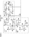
- FIG. 3 depicts a prior art sensing circuit 100. As can be seen in Figure 3 , the prior art design does not model the parasitic capacitance or otherwise take it into account.
- Sensing circuit 100 comprises memory data read block 110, memory reference read block 120, and differential amplifier block 130.
- Data read block 110 comprises current source 111, cascoding sensing NMOS transistor 113, bitline clamp NMOS transistor 114, diode connected sensing load PMOS transistor 112, and capacitor 115.
- Memory reference read block 120 comprises current source 121, reference bitline clamp NMOS transistor 124, cascoding sensing NMOS transistor 123, and diode connected sensing load PMOS transistor 122, and capacitor 125.
- Differential amplifier block 130 comprises input differential pair NMOS transistor 131 and 134, current mirror load PMOS transistor 132 and 133, output PMOS transistor 135, current bias NMOS transistor 136, output current bias NMOS transistor 137, and output 140.
- Node 116 is coupled to the selected memory cell (not shown) to be read, and node 117 is coupled to the reference memory cell (not shown) to be used to determine the value of the selected memory cell.
- Differential amplifier block 130 is used to compare the signals received from data read block 110 and reference read block 120 to generate output 140 which indicates the value of the data stored in the selected memory cell. These components are connected to one another as shown in Figure 3 .
- Sensing circuit 200 comprises memory data read block 210, memory reference read block 220, and differential amplifier block 230.
- Data read block 210 comprises current source 211, cascoding sensing NMOS transistor 213, bitline clamp NMOS transistor 214, diode connected sensing load PMOS transistor 212, and capacitor 215.
- Memory reference read block 220 comprises current source 221, reference bitline clamp NMOS transistor 224, cascoding sensing NMOS transistor 223, and diode connected sensing load PMOS transistor 222, and capacitor 225.
- Differential amplifier block 230 comprises input differential pair NMOS transistor 231 and 234, current mirror load PMOS transistor 232 and 233, output PMOS transistor 235, current bias NMOS transistor 236, output current bias NMOS transistor 237, and output 240.
- Node 216 is coupled to the selected memory cell (not shown) to be read, and node 217 is coupled to the reference memory cell (not shown) to be used to determine the value of the selected memory cell.
- Node 216 is the selected bit line and is coupled to capacitor 217 and capacitor 218, which each represents parasitic capacitance from adjacent bit lines, driven to compensate for capacitor 215, precharge switch 250 and equalization switch 260 are selectively turned on.
- the adjacent bit lines can be driven to a voltage VB, which is less than or equal to the voltage to which the selected bit line is driven. Doing so will reduce the effect of the parasitic capacitance represented by capacitor 217 and capacitor 218.
- Differential amplifier block 230 is used to compare the signals received from data read block 210 and reference read block 220 to generate output 240 which indicates the value of the data stored in the selected memory cell. These components are connected to one another as shown in Figure 4 .
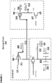
- FIG. 5 depicts another improved sensing circuit 300.
- Sensing circuit 300 comprises PMOS transistor 301, cascoding NMOS transistor 302, output PMOS transistor 308, current bias NMOS transistor 307, and output 310.
- Node 304 is coupled to the selected memory cell (not shown) to be read.
- the gate of transistor 301 receives pre-charge node voltage 309, which in this example can be 1.2 V or ground.
- the transistors 307, 308 constitutes single ended amplifier for the output. These components are connected to one another as shown in Figure 5 .
- the sensed node (gate of the transistor 308) is precharged to a bias level through the transistor 301 by the pre-charge node voltage 309 being ground. Then the pre-charge node voltage 309 going to a voltage level to release (weakly biased or turn off) the transistor 301.
- the sensed node will go down which turns on the transistor 308 to make the output 310 go high.
- Vsource voltage - bulk voltage small positive, e.g. 0.4v, less than Vp/n forward junction of ⁇ 0.6v
- Node 304 is coupled to capacitor 305 and capacitor 306, which each represents parasitic capacitance from an adjacent bit line, driven to compensate for , capacitor 303 connected to node 304.
- Sensing circuit 400 comprises PMOS transistor 401, cascoding NMOS transistor 403, output PMOS transistor 409, current bias NMOS transistor 410, and output 420.
- Node 405 is coupled to the selected memory cell (not shown) to be read, and node 412 is coupled to a reference memory cell (not shown).
- the gate of transistor 401 receives pre-charge node voltage 421, which in this example can be 1.2 V or ground.
- the transistors 409, 410 constitutes single ended amplifier for the output. These components are connected to one another as shown in Figure 6 .
- Vsource voltage - bulk voltage small positive, e.g. 0.4v, less than Vp/n forward junction of ⁇ 0.6v
- Node 405 is coupled to capacitor 406 and capacitor 407, which each represents parasitic capacitance from an adjacent bit line.
- Node 412 is coupled to capacitor 413 and capacitor 414, which each represents parasitic capacitance from an adjacent bit line, driven to compensate for capacitors 404and capacitor 411 and switches 402 and 408 are selectively turned on.
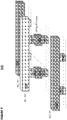
- Figure 7 depicts an improved layout 500 of bit lines to reduce parasitic capacitance between bit lines.
- Bit lines 510 and 530 are formed in one metal layer. However, bit line 520 is formed in a different metal layer. Thus, the distance between bit lines 510 and 520 and between bit lines 520 and 530 is longer than would be the case if bit line 520 were formed in the same metal layer as bit lines 510 and 530 as in the prior art.
- Bit line 520 connects to other circuit components through vias 560, metal 550, and connectors 540.
- Bit lines 510 and 530 connect to other circuit components through connectors 40.
- Figure 8 depicts the layout of Figure 7 from a top view. From this view, bit lines 510 and 520 and 530 appear adjacent to one another. However, as indicated by the different shading, bit line 520 and bit lines 510 and 530 are formed in different metal layers.
- Figure 9 depicts an improved layout 700 to reduce resistance of bit lines without increasing parasitic capacitance between bit lines.
- bit lines 510, 520, and 530 are adjacent, parallel, and formed in the same metal layer as in the prior art configuration.
- An additional structure 550 is placed above part of bit line 510 in a different metal layer and connects to bit line 510 through connectors 540.
- an additional structure 560 is placed above part of bit line 520 in a different metal layer and connects to bit line 520 through connectors 540
- an additional structure 570 is placed above part of bit line 530 in a different metal layer and connects to bit line 530 through connectors 540.
- Each additional structure 550, 560, and 570 has the effect of decreasing resistance of the bit line to which it connects but without increasing parasitic capacitance due to the length and placement of each additional structure.
- the additional structures 550, 560, and 570 are placed in a staggered format so that no significant parasitic capacitance is generated among or between them and bit lines 510, 520, and 530.
- Figure 10 depicts the layout of Figure 9 from a top view. Bit lines 510 and 520 and 530 are adjacent and parallel to one another. The staggered formation of additional structures 550, 560, and 570 is evident in this view.
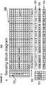
- Flash memory device 900 comprises: an array of memory cells 910, where the cells are accessed by word lines and bit lines; horizontal decoder 905; vertical decoder 920; read pulse control block 915; read control blocks 930; sense amplifier circuit blocks 925; and IO blocks 935.
- Read control blocks 930 are used to generate read timing pulses that track WL position, BL position, and IOwidth and to compensate for PVT.
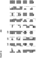
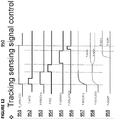
- Figure 12 depicts a timing diagram 950 showing the operation of various control signals over time.
- Signal 951 is the T_SEN-CYC signal
- signal 952 is the T-ATD signal
- signal 953 is the T-PRECHa signal
- signal 954 is the T-EQ signal
- signal 955 is the T-SENSEa signal
- signal 956 is the T-DOLATCH signal
- signal 957 is the T-BL0,BL1 signal
- signal 958 is the T-SO0,SO1 signal
- signal 959 is the T-SOUT signal.
- Signal 953 performs adaptive precharge pulsing.
- the pulse is shorter at WL0 (location 0 along the wordline) and longer at WL-N (location N along the wordline), and it is shorter at IO0 (location 0 along the IO line) and longer at IO-N (location N along the IO line).
- Signal 953 (T-PRECHa) tracks the WL delay and BL delay, for example, its pulses are shortest for WL0/BL0.
- T-SENSAa performs adaptive sensing pulsing.
- the pulse is shorter at IO0 and longer at IO-N.
- the pulse is shorter at WL0 and longer at WL-end. It tracks the WL delay and BL delay, for example, its pulses are longest for WL-N/BL-N.
- Signal 951(T-SEN-CYC) performs an automatic power down after a sense cycle has completed.
- Figure 13 depicts two graphs. The first graph shows that WL bias is higher at one end of the bitline than the other, and the second graph shows that BL bias is higher at one end of the bitline than the other. This shows the importance of decreasing the resistance of bitlines without increasing the parasitic capacitance between bitlines, as discussed previously with reference to Figures 9 and 10 .
Landscapes
- Read Only Memory (AREA)
- Semiconductor Memories (AREA)
- Non-Volatile Memory (AREA)
Claims (6)
- Flash-Speichervorrichtung, die Folgendes umfasst:eine erste Metallschicht (M1), die eine Gruppe von Bitleitungen zum Zugreifen auf Flash-Speicherzellen umfasst; undein zweites Metall (M2), das mehrere Strukturen umfasst, wobei jede Struktur aus den mehreren Strukturen mit einer Bitleitung aus der Gruppe von Bitleitungen in einer versetzten Formation verbunden ist, so dass der kürzeste Abstand zwischen irgendeinem Paar benachbarter Bitleitungen aus der Gruppe von Bitleitungen kleiner ist als der Abstand zwischen allen möglichen Paaren von Strukturen aus den mehreren Strukturen, die an den benachbarten Bitleitungen aus dem Paar benachbarter Bitleitungen angebracht sind, und wobei eine zweite Metallschichtstruktur, die an einer ersten Bitleitung angebracht ist, die Ebenen nicht schneidet, die senkrecht zu der zweiten Metallschichtstruktur sind, die an irgendeiner zweiten Bitleitung benachbart zu der ersten Bitleitung angebracht ist.
- Flash-Speichervorrichtung nach Anspruch 1, wobei jede Struktur aus den mehreren Strukturen in der zweiten Gruppe von Bitleitungen durch eine oder mehreren Durchkontaktierungen an die erste Metallschicht gekoppelt ist.
- Flash-Speichervorrichtung, die Folgendes umfasst:eine Anordnung von Flash-Speicherzellen, die in Reihen und Spalten organisiert sind;eine erste Metallschicht (M1), die eine Gruppe benachbarter Bitleitungen umfasst, wobei jede Bitleitung konfiguriert ist, auf eine Spalte aus Flash-Speicherzellen in der Anordnung zuzugreifen; undeine zweite Metallschicht (M2), die mehrere Strukturen umfasst, wobei jede Struktur aus den mehreren Strukturen an eine unterschiedliche Bitleitung aus der Gruppe benachbarter Bitleitungen gekoppelt ist und jede Struktur aus den mehreren Strukturen mit einer Bitleitung aus der Gruppe benachbarter Bitleitungen in einer versetzten Formation verbunden ist, so dass der kürzeste Abstand zwischen irgendeinem Paar benachbarter Bitleitungen in der Gruppe von Bitleitungen kleiner ist als der Abstand zwischen allen möglichen Paaren von Strukturen aus den mehreren Strukturen, die an den benachbarten Bitleitungen in dem Paar benachbarter Bitleitungen angebracht sind, und wobei eine zweite Metallschichtstruktur, die an einer ersten Bitleitung angebracht ist, die Ebenen nicht schneidet, die senkrecht zu der zweiten Metallschichtstruktur sind, die an irgendeiner zweiten Bitleitung benachbart zu der ersten Bitleitung angebracht ist.
- Flash-Speichervorrichtung nach Anspruch 3, wobei jede Struktur aus den mehreren Strukturen an eine unterschiedliche Bitleitung aus der Gruppe von Bitleitungen durch ein oder mehrere Verbindungselemente zwischen der ersten Metallschicht und der zweiten Metallschicht gekoppelt ist.
- Flash-Speichervorrichtung nach Anspruch 4, wobei jede Struktur aus den mehreren Strukturen kürzer ist als jede Bitleitung aus der Gruppe von Bitleitungen.
- Flash-Speichervorrichtung nach Anspruch 5, wobei die mehreren Strukturen in einer versetzten Formation innerhalb der zweiten Metallschicht angeordnet sind.
Priority Applications (1)
| Application Number | Priority Date | Filing Date | Title |
|---|---|---|---|
| EP17181079.9A EP3264416A3 (de) | 2013-03-15 | 2014-01-14 | Hochgeschwindigkeitserfassung für eine erweiterte nanometer-flashspeichervorrichtung |
Applications Claiming Priority (3)
| Application Number | Priority Date | Filing Date | Title |
|---|---|---|---|
| US201361799970P | 2013-03-15 | 2013-03-15 | |
| US13/958,415 US20140269061A1 (en) | 2013-03-15 | 2013-08-02 | High Speed Sensing For Advanced Nanometer Flash Memory Device |
| PCT/US2014/011554 WO2014149166A1 (en) | 2013-03-15 | 2014-01-14 | High speed sensing for advanced nanometer flash memory device |
Related Child Applications (2)
| Application Number | Title | Priority Date | Filing Date |
|---|---|---|---|
| EP17181079.9A Division EP3264416A3 (de) | 2013-03-15 | 2014-01-14 | Hochgeschwindigkeitserfassung für eine erweiterte nanometer-flashspeichervorrichtung |
| EP17181079.9A Division-Into EP3264416A3 (de) | 2013-03-15 | 2014-01-14 | Hochgeschwindigkeitserfassung für eine erweiterte nanometer-flashspeichervorrichtung |
Publications (2)
| Publication Number | Publication Date |
|---|---|
| EP2973708A1 EP2973708A1 (de) | 2016-01-20 |
| EP2973708B1 true EP2973708B1 (de) | 2017-10-18 |
Family
ID=51526478
Family Applications (2)
| Application Number | Title | Priority Date | Filing Date |
|---|---|---|---|
| EP14702703.1A Active EP2973708B1 (de) | 2013-03-15 | 2014-01-14 | Hochgeschwindigkeitserfassung für eine erweiterte nanometer-flashspeichervorrichtung |
| EP17181079.9A Ceased EP3264416A3 (de) | 2013-03-15 | 2014-01-14 | Hochgeschwindigkeitserfassung für eine erweiterte nanometer-flashspeichervorrichtung |
Family Applications After (1)
| Application Number | Title | Priority Date | Filing Date |
|---|---|---|---|
| EP17181079.9A Ceased EP3264416A3 (de) | 2013-03-15 | 2014-01-14 | Hochgeschwindigkeitserfassung für eine erweiterte nanometer-flashspeichervorrichtung |
Country Status (7)
| Country | Link |
|---|---|
| US (2) | US20140269061A1 (de) |
| EP (2) | EP2973708B1 (de) |
| JP (2) | JP2016514366A (de) |
| KR (1) | KR101691319B1 (de) |
| CN (2) | CN104937718B (de) |
| TW (1) | TWI545697B (de) |
| WO (1) | WO2014149166A1 (de) |
Families Citing this family (11)
| Publication number | Priority date | Publication date | Assignee | Title |
|---|---|---|---|---|
| CN106782649B (zh) * | 2015-11-20 | 2020-07-14 | 华邦电子股份有限公司 | 感测放大器电路 |
| CN106935267B (zh) * | 2015-12-31 | 2020-11-10 | 硅存储技术公司 | 用于闪速存储器系统的低功率感测放大器 |
| US10149377B2 (en) * | 2016-06-24 | 2018-12-04 | Invensas Corporation | Stacked transmission line |
| CN110610738B (zh) * | 2018-06-15 | 2023-08-18 | 硅存储技术公司 | 用于闪存存储器系统的改进的感测放大器 |
| JP2020102290A (ja) | 2018-12-21 | 2020-07-02 | キオクシア株式会社 | 半導体記憶装置 |
| CN110704332B (zh) * | 2019-08-29 | 2021-11-09 | 深圳大普微电子科技有限公司 | 一种闪存介质优化方法及非易失性存储设备 |
| WO2021226816A1 (en) * | 2020-05-12 | 2021-11-18 | Yangtze Advanced Memory Industrial Innovation Center Co., Ltd | A novel distributed array and contact architecture for 4 stack 3d pcm memory |
| US12450472B2 (en) * | 2020-06-22 | 2025-10-21 | Qualcomm Incorporated | Charge-pump-based current-mode neuron for machine learning |
| CN114171083B (zh) | 2020-11-03 | 2025-05-06 | 台湾积体电路制造股份有限公司 | 存储器器件 |
| CN117015229A (zh) * | 2022-04-26 | 2023-11-07 | 长鑫存储技术有限公司 | 三维存储器及其形成方法 |
| US20260038578A1 (en) * | 2024-07-30 | 2026-02-05 | Micron Technology, Inc. | Sense amplifier balancing component |
Family Cites Families (37)
| Publication number | Priority date | Publication date | Assignee | Title |
|---|---|---|---|---|
| JPH06195990A (ja) * | 1992-12-21 | 1994-07-15 | Kawasaki Steel Corp | 半導体記憶装置 |
| US6108237A (en) * | 1997-07-17 | 2000-08-22 | Micron Technology, Inc. | Fast-sensing amplifier for flash memory |
| EP0808502B1 (de) * | 1995-02-10 | 2002-05-22 | Micron Technology, Inc. | Schneller leseverstärker für einen flash-speicher |
| DE69702256T2 (de) * | 1996-06-24 | 2001-01-18 | Advanced Micro Devices, Inc. | Verfahren für einen merhfachen, bits pro zelle flash eeprom, speicher mit seitenprogrammierungsmodus und leseverfahren |
| JPH11134891A (ja) * | 1997-10-31 | 1999-05-21 | Sanyo Electric Co Ltd | 半導体メモリ装置 |
| JP2002057227A (ja) * | 2000-08-11 | 2002-02-22 | Mitsubishi Electric Corp | 半導体記憶装置 |
| JP2004111478A (ja) * | 2002-09-13 | 2004-04-08 | Sharp Corp | 不揮発性半導体記憶装置およびその製造方法 |
| JP2004119457A (ja) * | 2002-09-24 | 2004-04-15 | Matsushita Electric Ind Co Ltd | 半導体記憶装置 |
| JP4012144B2 (ja) * | 2003-12-25 | 2007-11-21 | 株式会社東芝 | 半導体記憶装置 |
| US7177176B2 (en) * | 2004-06-30 | 2007-02-13 | Intel Corporation | Six-transistor (6T) static random access memory (SRAM) with dynamically variable p-channel metal oxide semiconductor (PMOS) strength |
| CN101203919A (zh) * | 2005-03-04 | 2008-06-18 | 爱特梅尔公司 | 用于寄存器文件的快速读取端口 |
| KR100632656B1 (ko) * | 2005-05-23 | 2006-10-11 | 주식회사 하이닉스반도체 | 플래쉬 메모리소자의 비트라인 형성방법 |
| CN100395843C (zh) * | 2005-06-02 | 2008-06-18 | 复旦大学 | 高速低功耗电流灵敏放大器 |
| KR100675517B1 (ko) * | 2005-09-09 | 2007-01-30 | 주식회사 엑셀반도체 | 시리얼 플래쉬 메모리 장치 및 프리차아지 방법 |
| JP2007080424A (ja) * | 2005-09-15 | 2007-03-29 | Renesas Technology Corp | 不揮発性メモリ |
| US7638878B2 (en) * | 2006-04-13 | 2009-12-29 | Micron Technology, Inc. | Devices and systems including the bit lines and bit line contacts |
| JP2008047189A (ja) * | 2006-08-11 | 2008-02-28 | Matsushita Electric Ind Co Ltd | 半導体記憶装置 |
| US7675783B2 (en) * | 2007-02-27 | 2010-03-09 | Samsung Electronics Co., Ltd. | Nonvolatile memory device and driving method thereof |
| JP4504397B2 (ja) * | 2007-05-29 | 2010-07-14 | 株式会社東芝 | 半導体記憶装置 |
| US7755962B2 (en) * | 2007-07-09 | 2010-07-13 | Samsung Electronics Co., Ltd. | Semiconductor memory devices, memory systems and computing systems including the same |
| JP2009016016A (ja) * | 2007-07-09 | 2009-01-22 | Samsung Electronics Co Ltd | 半導体集積回路 |
| US7697365B2 (en) * | 2007-07-13 | 2010-04-13 | Silicon Storage Technology, Inc. | Sub volt flash memory system |
| US7977709B2 (en) * | 2008-01-02 | 2011-07-12 | Infineon Technologies Ag | MOS transistor and semiconductor device |
| JP5554935B2 (ja) * | 2008-03-17 | 2014-07-23 | ピーエスフォー ルクスコ エスエイアールエル | 半導体装置 |
| KR101468149B1 (ko) * | 2008-09-19 | 2014-12-03 | 삼성전자주식회사 | 플래시 메모리 장치 및 시스템들 그리고 그것의 읽기 방법 |
| US8018773B2 (en) | 2009-03-04 | 2011-09-13 | Silicon Storage Technology, Inc. | Array of non-volatile memory cells including embedded local and global reference cells and system |
| KR20110056005A (ko) * | 2009-11-20 | 2011-05-26 | 삼성전자주식회사 | 반도체 장치의 배선 구조체 |
| CN102081959B (zh) * | 2009-11-26 | 2013-06-12 | 中国科学院微电子研究所 | 一种存储器读出电路以及存储器 |
| JP2011138569A (ja) * | 2009-12-25 | 2011-07-14 | Toshiba Corp | 不揮発性半導体記憶装置 |
| US8385147B2 (en) * | 2010-03-30 | 2013-02-26 | Silicon Storage Technology, Inc. | Systems and methods of non-volatile memory sensing including selective/differential threshold voltage features |
| US8274828B2 (en) * | 2010-12-15 | 2012-09-25 | Fs Semiconductor Corp., Ltd. | Structures and methods for reading out non-volatile memory using referencing cells |
| JP4982606B2 (ja) * | 2010-12-22 | 2012-07-25 | 株式会社東芝 | 半導体記憶装置およびその制御方法 |
| US8605521B2 (en) * | 2011-05-12 | 2013-12-10 | Micron Technology, Inc. | Sense amplifiers, memories, and apparatuses and methods for sensing a data state of a memory cell |
| US8320211B1 (en) * | 2011-05-16 | 2012-11-27 | National Tsing Hua University | Current-sense amplifier with low-offset adjustment and method of low-offset adjustment thereof |
| CN202534357U (zh) * | 2012-03-19 | 2012-11-14 | 河南科技大学 | 一种用于铁电随机存储器读出电路的电流型灵敏放大器 |
| KR101916192B1 (ko) * | 2012-04-19 | 2018-11-07 | 삼성전자주식회사 | 플래그 셀을 포함하는 불휘발성 메모리 장치 및 그것의 사용자 장치 |
| US8928406B2 (en) * | 2013-03-13 | 2015-01-06 | Texas Instruments Incorporated | Low-power inverter-based differential amplifier |
-
2013
- 2013-08-02 US US13/958,415 patent/US20140269061A1/en not_active Abandoned
-
2014
- 2014-01-14 JP JP2015560182A patent/JP2016514366A/ja active Pending
- 2014-01-14 EP EP14702703.1A patent/EP2973708B1/de active Active
- 2014-01-14 KR KR1020157020604A patent/KR101691319B1/ko active Active
- 2014-01-14 WO PCT/US2014/011554 patent/WO2014149166A1/en not_active Ceased
- 2014-01-14 CN CN201480005640.XA patent/CN104937718B/zh active Active
- 2014-01-14 EP EP17181079.9A patent/EP3264416A3/de not_active Ceased
- 2014-01-14 CN CN201810146062.1A patent/CN108198581B/zh active Active
- 2014-01-21 TW TW103102093A patent/TWI545697B/zh active
-
2017
- 2017-10-24 US US15/792,590 patent/US10283206B2/en active Active
-
2018
- 2018-01-16 JP JP2018004736A patent/JP6676081B2/ja active Active
Non-Patent Citations (1)
| Title |
|---|
| None * |
Also Published As
| Publication number | Publication date |
|---|---|
| EP3264416A3 (de) | 2018-04-04 |
| KR20150103708A (ko) | 2015-09-11 |
| EP3264416A2 (de) | 2018-01-03 |
| KR101691319B1 (ko) | 2016-12-29 |
| JP2016514366A (ja) | 2016-05-19 |
| CN108198581B (zh) | 2023-04-07 |
| CN104937718A (zh) | 2015-09-23 |
| US20140269061A1 (en) | 2014-09-18 |
| JP6676081B2 (ja) | 2020-04-08 |
| TWI545697B (zh) | 2016-08-11 |
| WO2014149166A1 (en) | 2014-09-25 |
| EP2973708A1 (de) | 2016-01-20 |
| JP2018101457A (ja) | 2018-06-28 |
| CN104937718B (zh) | 2018-03-06 |
| US10283206B2 (en) | 2019-05-07 |
| TW201440174A (zh) | 2014-10-16 |
| US20180047454A1 (en) | 2018-02-15 |
| CN108198581A (zh) | 2018-06-22 |
Similar Documents
| Publication | Publication Date | Title |
|---|---|---|
| EP2973708B1 (de) | Hochgeschwindigkeitserfassung für eine erweiterte nanometer-flashspeichervorrichtung | |
| US10176878B2 (en) | Sense amplifier and memory device using the same | |
| US9953717B2 (en) | NAND structure with tier select gate transistors | |
| US9922716B2 (en) | Architecture for CMOS under array | |
| TWI841928B (zh) | 半導體記憶裝置及於半導體記憶裝置中執行讀出動作之方法 | |
| KR101001449B1 (ko) | 불휘발성 소자의 독출 동작 방법 | |
| KR101088954B1 (ko) | 프로그램이 가능한 비휘발성 메모리 | |
| US10276792B2 (en) | Low power barrier modulated cell for storage class memory | |
| US10878907B1 (en) | Sub-block size reduction for 3D non-volatile memory | |
| WO2018038783A1 (en) | 3d nand with partial block erase | |
| CN101989454B (zh) | 半导体存储器件及其操作方法 | |
| US9543030B1 (en) | Sense amplifier design for ramp sensing | |
| US9361976B2 (en) | Sense amplifier including a single-transistor amplifier and level shifter and methods therefor | |
| US9324430B2 (en) | Method for defining a default state of a charge trap based memory cell | |
| KR101231478B1 (ko) | 서브어레이의 에지에서 액세스 디바이스를 사용하는 디지트 라인 평형 유지 | |
| TW201503140A (zh) | 用於反及閘快閃記憶體裝置之友善光刻局部讀取電路及其製造方法 | |
| KR20210070219A (ko) | 데이터 라인 설정 동작과 동시에 시딩 동작을 위한 장치 및 방법 | |
| US9224466B1 (en) | Dual capacitor sense amplifier and methods therefor | |
| CN102789807B (zh) | 具有二极管在存储串列中的三维阵列存储器架构 | |
| TWI497524B (zh) | 記憶體頁面緩衝器 |
Legal Events
| Date | Code | Title | Description |
|---|---|---|---|
| PUAI | Public reference made under article 153(3) epc to a published international application that has entered the european phase |
Free format text: ORIGINAL CODE: 0009012 |
|
| 17P | Request for examination filed |
Effective date: 20151015 |
|
| AK | Designated contracting states |
Kind code of ref document: A1 Designated state(s): AL AT BE BG CH CY CZ DE DK EE ES FI FR GB GR HR HU IE IS IT LI LT LU LV MC MK MT NL NO PL PT RO RS SE SI SK SM TR |
|
| AX | Request for extension of the european patent |
Extension state: BA ME |
|
| DAX | Request for extension of the european patent (deleted) | ||
| 17Q | First examination report despatched |
Effective date: 20161006 |
|
| GRAP | Despatch of communication of intention to grant a patent |
Free format text: ORIGINAL CODE: EPIDOSNIGR1 |
|
| INTG | Intention to grant announced |
Effective date: 20170511 |
|
| GRAS | Grant fee paid |
Free format text: ORIGINAL CODE: EPIDOSNIGR3 |
|
| GRAA | (expected) grant |
Free format text: ORIGINAL CODE: 0009210 |
|
| AK | Designated contracting states |
Kind code of ref document: B1 Designated state(s): AL AT BE BG CH CY CZ DE DK EE ES FI FR GB GR HR HU IE IS IT LI LT LU LV MC MK MT NL NO PL PT RO RS SE SI SK SM TR |
|
| REG | Reference to a national code |
Ref country code: GB Ref legal event code: FG4D |
|
| REG | Reference to a national code |
Ref country code: CH Ref legal event code: EP |
|
| REG | Reference to a national code |
Ref country code: AT Ref legal event code: REF Ref document number: 938638 Country of ref document: AT Kind code of ref document: T Effective date: 20171115 Ref country code: IE Ref legal event code: FG4D |
|
| REG | Reference to a national code |
Ref country code: DE Ref legal event code: R096 Ref document number: 602014015928 Country of ref document: DE |
|
| REG | Reference to a national code |
Ref country code: FR Ref legal event code: PLFP Year of fee payment: 5 |
|
| REG | Reference to a national code |
Ref country code: NL Ref legal event code: FP |
|
| REG | Reference to a national code |
Ref country code: LT Ref legal event code: MG4D |
|
| PG25 | Lapsed in a contracting state [announced via postgrant information from national office to epo] |
Ref country code: FI Free format text: LAPSE BECAUSE OF FAILURE TO SUBMIT A TRANSLATION OF THE DESCRIPTION OR TO PAY THE FEE WITHIN THE PRESCRIBED TIME-LIMIT Effective date: 20171018 Ref country code: ES Free format text: LAPSE BECAUSE OF FAILURE TO SUBMIT A TRANSLATION OF THE DESCRIPTION OR TO PAY THE FEE WITHIN THE PRESCRIBED TIME-LIMIT Effective date: 20171018 Ref country code: LT Free format text: LAPSE BECAUSE OF FAILURE TO SUBMIT A TRANSLATION OF THE DESCRIPTION OR TO PAY THE FEE WITHIN THE PRESCRIBED TIME-LIMIT Effective date: 20171018 Ref country code: NO Free format text: LAPSE BECAUSE OF FAILURE TO SUBMIT A TRANSLATION OF THE DESCRIPTION OR TO PAY THE FEE WITHIN THE PRESCRIBED TIME-LIMIT Effective date: 20180118 Ref country code: SE Free format text: LAPSE BECAUSE OF FAILURE TO SUBMIT A TRANSLATION OF THE DESCRIPTION OR TO PAY THE FEE WITHIN THE PRESCRIBED TIME-LIMIT Effective date: 20171018 |
|
| PG25 | Lapsed in a contracting state [announced via postgrant information from national office to epo] |
Ref country code: BG Free format text: LAPSE BECAUSE OF FAILURE TO SUBMIT A TRANSLATION OF THE DESCRIPTION OR TO PAY THE FEE WITHIN THE PRESCRIBED TIME-LIMIT Effective date: 20180118 Ref country code: IS Free format text: LAPSE BECAUSE OF FAILURE TO SUBMIT A TRANSLATION OF THE DESCRIPTION OR TO PAY THE FEE WITHIN THE PRESCRIBED TIME-LIMIT Effective date: 20180218 Ref country code: HR Free format text: LAPSE BECAUSE OF FAILURE TO SUBMIT A TRANSLATION OF THE DESCRIPTION OR TO PAY THE FEE WITHIN THE PRESCRIBED TIME-LIMIT Effective date: 20171018 Ref country code: LV Free format text: LAPSE BECAUSE OF FAILURE TO SUBMIT A TRANSLATION OF THE DESCRIPTION OR TO PAY THE FEE WITHIN THE PRESCRIBED TIME-LIMIT Effective date: 20171018 Ref country code: RS Free format text: LAPSE BECAUSE OF FAILURE TO SUBMIT A TRANSLATION OF THE DESCRIPTION OR TO PAY THE FEE WITHIN THE PRESCRIBED TIME-LIMIT Effective date: 20171018 Ref country code: GR Free format text: LAPSE BECAUSE OF FAILURE TO SUBMIT A TRANSLATION OF THE DESCRIPTION OR TO PAY THE FEE WITHIN THE PRESCRIBED TIME-LIMIT Effective date: 20180119 |
|
| REG | Reference to a national code |
Ref country code: DE Ref legal event code: R097 Ref document number: 602014015928 Country of ref document: DE |
|
| PG25 | Lapsed in a contracting state [announced via postgrant information from national office to epo] |
Ref country code: CZ Free format text: LAPSE BECAUSE OF FAILURE TO SUBMIT A TRANSLATION OF THE DESCRIPTION OR TO PAY THE FEE WITHIN THE PRESCRIBED TIME-LIMIT Effective date: 20171018 Ref country code: DK Free format text: LAPSE BECAUSE OF FAILURE TO SUBMIT A TRANSLATION OF THE DESCRIPTION OR TO PAY THE FEE WITHIN THE PRESCRIBED TIME-LIMIT Effective date: 20171018 Ref country code: EE Free format text: LAPSE BECAUSE OF FAILURE TO SUBMIT A TRANSLATION OF THE DESCRIPTION OR TO PAY THE FEE WITHIN THE PRESCRIBED TIME-LIMIT Effective date: 20171018 Ref country code: SK Free format text: LAPSE BECAUSE OF FAILURE TO SUBMIT A TRANSLATION OF THE DESCRIPTION OR TO PAY THE FEE WITHIN THE PRESCRIBED TIME-LIMIT Effective date: 20171018 |
|
| PLBE | No opposition filed within time limit |
Free format text: ORIGINAL CODE: 0009261 |
|
| STAA | Information on the status of an ep patent application or granted ep patent |
Free format text: STATUS: NO OPPOSITION FILED WITHIN TIME LIMIT |
|
| PG25 | Lapsed in a contracting state [announced via postgrant information from national office to epo] |
Ref country code: RO Free format text: LAPSE BECAUSE OF FAILURE TO SUBMIT A TRANSLATION OF THE DESCRIPTION OR TO PAY THE FEE WITHIN THE PRESCRIBED TIME-LIMIT Effective date: 20171018 Ref country code: PL Free format text: LAPSE BECAUSE OF FAILURE TO SUBMIT A TRANSLATION OF THE DESCRIPTION OR TO PAY THE FEE WITHIN THE PRESCRIBED TIME-LIMIT Effective date: 20171018 Ref country code: SM Free format text: LAPSE BECAUSE OF FAILURE TO SUBMIT A TRANSLATION OF THE DESCRIPTION OR TO PAY THE FEE WITHIN THE PRESCRIBED TIME-LIMIT Effective date: 20171018 |
|
| REG | Reference to a national code |
Ref country code: CH Ref legal event code: PL |
|
| 26N | No opposition filed |
Effective date: 20180719 |
|
| PG25 | Lapsed in a contracting state [announced via postgrant information from national office to epo] |
Ref country code: LU Free format text: LAPSE BECAUSE OF NON-PAYMENT OF DUE FEES Effective date: 20180114 |
|
| REG | Reference to a national code |
Ref country code: IE Ref legal event code: MM4A |
|
| REG | Reference to a national code |
Ref country code: BE Ref legal event code: MM Effective date: 20180131 |
|
| PG25 | Lapsed in a contracting state [announced via postgrant information from national office to epo] |
Ref country code: CH Free format text: LAPSE BECAUSE OF NON-PAYMENT OF DUE FEES Effective date: 20180131 Ref country code: LI Free format text: LAPSE BECAUSE OF NON-PAYMENT OF DUE FEES Effective date: 20180131 Ref country code: BE Free format text: LAPSE BECAUSE OF NON-PAYMENT OF DUE FEES Effective date: 20180131 Ref country code: SI Free format text: LAPSE BECAUSE OF FAILURE TO SUBMIT A TRANSLATION OF THE DESCRIPTION OR TO PAY THE FEE WITHIN THE PRESCRIBED TIME-LIMIT Effective date: 20171018 |
|
| PG25 | Lapsed in a contracting state [announced via postgrant information from national office to epo] |
Ref country code: IE Free format text: LAPSE BECAUSE OF NON-PAYMENT OF DUE FEES Effective date: 20180114 |
|
| PG25 | Lapsed in a contracting state [announced via postgrant information from national office to epo] |
Ref country code: MC Free format text: LAPSE BECAUSE OF FAILURE TO SUBMIT A TRANSLATION OF THE DESCRIPTION OR TO PAY THE FEE WITHIN THE PRESCRIBED TIME-LIMIT Effective date: 20171018 |
|
| PG25 | Lapsed in a contracting state [announced via postgrant information from national office to epo] |
Ref country code: MT Free format text: LAPSE BECAUSE OF NON-PAYMENT OF DUE FEES Effective date: 20180114 |
|
| REG | Reference to a national code |
Ref country code: AT Ref legal event code: UEP Ref document number: 938638 Country of ref document: AT Kind code of ref document: T Effective date: 20171018 |
|
| PG25 | Lapsed in a contracting state [announced via postgrant information from national office to epo] |
Ref country code: TR Free format text: LAPSE BECAUSE OF FAILURE TO SUBMIT A TRANSLATION OF THE DESCRIPTION OR TO PAY THE FEE WITHIN THE PRESCRIBED TIME-LIMIT Effective date: 20171018 |
|
| PG25 | Lapsed in a contracting state [announced via postgrant information from national office to epo] |
Ref country code: PT Free format text: LAPSE BECAUSE OF FAILURE TO SUBMIT A TRANSLATION OF THE DESCRIPTION OR TO PAY THE FEE WITHIN THE PRESCRIBED TIME-LIMIT Effective date: 20171018 |
|
| PG25 | Lapsed in a contracting state [announced via postgrant information from national office to epo] |
Ref country code: CY Free format text: LAPSE BECAUSE OF FAILURE TO SUBMIT A TRANSLATION OF THE DESCRIPTION OR TO PAY THE FEE WITHIN THE PRESCRIBED TIME-LIMIT Effective date: 20171018 Ref country code: HU Free format text: LAPSE BECAUSE OF FAILURE TO SUBMIT A TRANSLATION OF THE DESCRIPTION OR TO PAY THE FEE WITHIN THE PRESCRIBED TIME-LIMIT; INVALID AB INITIO Effective date: 20140114 Ref country code: MK Free format text: LAPSE BECAUSE OF NON-PAYMENT OF DUE FEES Effective date: 20171018 |
|
| PG25 | Lapsed in a contracting state [announced via postgrant information from national office to epo] |
Ref country code: AL Free format text: LAPSE BECAUSE OF FAILURE TO SUBMIT A TRANSLATION OF THE DESCRIPTION OR TO PAY THE FEE WITHIN THE PRESCRIBED TIME-LIMIT Effective date: 20171018 |
|
| REG | Reference to a national code |
Ref country code: DE Ref legal event code: R079 Ref document number: 602014015928 Country of ref document: DE Free format text: PREVIOUS MAIN CLASS: H01L0027115000 Ipc: H10B0069000000 |
|
| P01 | Opt-out of the competence of the unified patent court (upc) registered |
Effective date: 20230528 |
|
| PGFP | Annual fee paid to national office [announced via postgrant information from national office to epo] |
Ref country code: GB Payment date: 20251220 Year of fee payment: 13 |
|
| PGFP | Annual fee paid to national office [announced via postgrant information from national office to epo] |
Ref country code: FR Payment date: 20251217 Year of fee payment: 13 Ref country code: NL Payment date: 20251217 Year of fee payment: 13 |
|
| PGFP | Annual fee paid to national office [announced via postgrant information from national office to epo] |
Ref country code: DE Payment date: 20251217 Year of fee payment: 13 |
|
| PGFP | Annual fee paid to national office [announced via postgrant information from national office to epo] |
Ref country code: AT Payment date: 20251218 Year of fee payment: 13 |
|
| PGFP | Annual fee paid to national office [announced via postgrant information from national office to epo] |
Ref country code: IT Payment date: 20260107 Year of fee payment: 13 |