EP2630675B1 - Dispositif électroluminescent organique et procédé associé - Google Patents
Dispositif électroluminescent organique et procédé associé Download PDFInfo
- Publication number
- EP2630675B1 EP2630675B1 EP11781577.9A EP11781577A EP2630675B1 EP 2630675 B1 EP2630675 B1 EP 2630675B1 EP 11781577 A EP11781577 A EP 11781577A EP 2630675 B1 EP2630675 B1 EP 2630675B1
- Authority
- EP
- European Patent Office
- Prior art keywords
- light
- layer
- emitting
- charge
- polymer
- Prior art date
- Legal status (The legal status is an assumption and is not a legal conclusion. Google has not performed a legal analysis and makes no representation as to the accuracy of the status listed.)
- Active
Links
- 238000000034 method Methods 0.000 title claims description 14
- 229920000642 polymer Polymers 0.000 claims description 96
- 239000000463 material Substances 0.000 claims description 60
- 239000002019 doping agent Substances 0.000 claims description 49
- 125000001424 substituent group Chemical group 0.000 claims description 29
- 125000001072 heteroaryl group Chemical group 0.000 claims description 28
- 125000003118 aryl group Chemical group 0.000 claims description 20
- 238000000151 deposition Methods 0.000 claims description 11
- 239000002904 solvent Substances 0.000 claims description 9
- 125000005264 aryl amine group Chemical group 0.000 claims description 8
- 125000003107 substituted aryl group Chemical group 0.000 claims description 8
- 230000008021 deposition Effects 0.000 claims description 6
- 125000005647 linker group Chemical group 0.000 claims description 2
- 230000005525 hole transport Effects 0.000 description 43
- 230000000052 comparative effect Effects 0.000 description 19
- 125000000217 alkyl group Chemical group 0.000 description 18
- 229910052751 metal Inorganic materials 0.000 description 17
- 239000002184 metal Substances 0.000 description 17
- 239000000178 monomer Substances 0.000 description 12
- 229910052760 oxygen Inorganic materials 0.000 description 12
- 0 C*c1ccc(*(c2ccc(C)cc2*2)c3c2cc(C)cc3)cc1 Chemical compound C*c1ccc(*(c2ccc(C)cc2*2)c3c2cc(C)cc3)cc1 0.000 description 10
- 125000001997 phenyl group Chemical group [H]C1=C([H])C([H])=C(*)C([H])=C1[H] 0.000 description 10
- 125000003837 (C1-C20) alkyl group Chemical group 0.000 description 9
- 239000003446 ligand Substances 0.000 description 9
- 229910052757 nitrogen Inorganic materials 0.000 description 9
- 239000000243 solution Substances 0.000 description 9
- 239000000758 substrate Substances 0.000 description 9
- 229910052799 carbon Inorganic materials 0.000 description 8
- 230000005281 excited state Effects 0.000 description 8
- 238000002347 injection Methods 0.000 description 8
- 239000007924 injection Substances 0.000 description 8
- -1 poly(phenylenevinylene) Polymers 0.000 description 8
- IJGRMHOSHXDMSA-UHFFFAOYSA-N Atomic nitrogen Chemical compound N#N IJGRMHOSHXDMSA-UHFFFAOYSA-N 0.000 description 7
- 229920001577 copolymer Polymers 0.000 description 7
- 125000000732 arylene group Chemical group 0.000 description 6
- 239000011368 organic material Substances 0.000 description 6
- 238000005215 recombination Methods 0.000 description 6
- 230000006798 recombination Effects 0.000 description 6
- 229910052717 sulfur Inorganic materials 0.000 description 6
- 125000003545 alkoxy group Chemical group 0.000 description 5
- QVGXLLKOCUKJST-UHFFFAOYSA-N atomic oxygen Chemical compound [O] QVGXLLKOCUKJST-UHFFFAOYSA-N 0.000 description 5
- 125000004432 carbon atom Chemical group C* 0.000 description 5
- 239000011521 glass Substances 0.000 description 5
- 239000011159 matrix material Substances 0.000 description 5
- 150000002739 metals Chemical class 0.000 description 5
- 239000001301 oxygen Substances 0.000 description 5
- 229920003023 plastic Polymers 0.000 description 5
- 239000004033 plastic Substances 0.000 description 5
- 238000004528 spin coating Methods 0.000 description 5
- 125000001140 1,4-phenylene group Chemical group [H]C1=C([H])C([*:2])=C([H])C([H])=C1[*:1] 0.000 description 4
- KDLHZDBZIXYQEI-UHFFFAOYSA-N Palladium Chemical compound [Pd] KDLHZDBZIXYQEI-UHFFFAOYSA-N 0.000 description 4
- JUJWROOIHBZHMG-UHFFFAOYSA-N Pyridine Chemical compound C1=CC=NC=C1 JUJWROOIHBZHMG-UHFFFAOYSA-N 0.000 description 4
- VYPSYNLAJGMNEJ-UHFFFAOYSA-N Silicium dioxide Chemical compound O=[Si]=O VYPSYNLAJGMNEJ-UHFFFAOYSA-N 0.000 description 4
- 239000004411 aluminium Substances 0.000 description 4
- 229910052782 aluminium Inorganic materials 0.000 description 4
- XAGFODPZIPBFFR-UHFFFAOYSA-N aluminium Chemical compound [Al] XAGFODPZIPBFFR-UHFFFAOYSA-N 0.000 description 4
- 230000001627 detrimental effect Effects 0.000 description 4
- 239000008393 encapsulating agent Substances 0.000 description 4
- 125000003983 fluorenyl group Chemical group C1(=CC=CC=2C3=CC=CC=C3CC12)* 0.000 description 4
- 229910052731 fluorine Inorganic materials 0.000 description 4
- 239000011737 fluorine Substances 0.000 description 4
- 229910052736 halogen Inorganic materials 0.000 description 4
- 150000002367 halogens Chemical class 0.000 description 4
- 230000003993 interaction Effects 0.000 description 4
- 239000000203 mixture Substances 0.000 description 4
- 125000000843 phenylene group Chemical group C1(=C(C=CC=C1)*)* 0.000 description 4
- 229920002098 polyfluorene Polymers 0.000 description 4
- LIVNPJMFVYWSIS-UHFFFAOYSA-N silicon monoxide Chemical compound [Si-]#[O+] LIVNPJMFVYWSIS-UHFFFAOYSA-N 0.000 description 4
- 238000010129 solution processing Methods 0.000 description 4
- ZOXJGFHDIHLPTG-UHFFFAOYSA-N Boron Chemical group [B] ZOXJGFHDIHLPTG-UHFFFAOYSA-N 0.000 description 3
- WKBOTKDWSSQWDR-UHFFFAOYSA-N Bromine atom Chemical compound [Br] WKBOTKDWSSQWDR-UHFFFAOYSA-N 0.000 description 3
- OKTJSMMVPCPJKN-UHFFFAOYSA-N Carbon Chemical compound [C] OKTJSMMVPCPJKN-UHFFFAOYSA-N 0.000 description 3
- PXGOKWXKJXAPGV-UHFFFAOYSA-N Fluorine Chemical compound FF PXGOKWXKJXAPGV-UHFFFAOYSA-N 0.000 description 3
- 229920001609 Poly(3,4-ethylenedioxythiophene) Polymers 0.000 description 3
- YXFVVABEGXRONW-UHFFFAOYSA-N Toluene Chemical compound CC1=CC=CC=C1 YXFVVABEGXRONW-UHFFFAOYSA-N 0.000 description 3
- 125000004429 atom Chemical group 0.000 description 3
- 230000004888 barrier function Effects 0.000 description 3
- UMIVXZPTRXBADB-UHFFFAOYSA-N benzocyclobutene Chemical group C1=CC=C2CCC2=C1 UMIVXZPTRXBADB-UHFFFAOYSA-N 0.000 description 3
- GDTBXPJZTBHREO-UHFFFAOYSA-N bromine Substances BrBr GDTBXPJZTBHREO-UHFFFAOYSA-N 0.000 description 3
- 229910052794 bromium Inorganic materials 0.000 description 3
- 239000003054 catalyst Substances 0.000 description 3
- 230000008859 change Effects 0.000 description 3
- 125000004093 cyano group Chemical group *C#N 0.000 description 3
- 239000000412 dendrimer Substances 0.000 description 3
- AMGQUBHHOARCQH-UHFFFAOYSA-N indium;oxotin Chemical compound [In].[Sn]=O AMGQUBHHOARCQH-UHFFFAOYSA-N 0.000 description 3
- 238000007641 inkjet printing Methods 0.000 description 3
- 229920000412 polyarylene Polymers 0.000 description 3
- 238000007639 printing Methods 0.000 description 3
- 238000012546 transfer Methods 0.000 description 3
- GGUFVZFOCZNPEG-UHFFFAOYSA-N 4,5,6-triphenyltriazine Chemical group C1=CC=CC=C1C1=NN=NC(C=2C=CC=CC=2)=C1C1=CC=CC=C1 GGUFVZFOCZNPEG-UHFFFAOYSA-N 0.000 description 2
- UJOBWOGCFQCDNV-UHFFFAOYSA-N 9H-carbazole Chemical compound C1=CC=C2C3=CC=CC=C3NC2=C1 UJOBWOGCFQCDNV-UHFFFAOYSA-N 0.000 description 2
- ZAMOUSCENKQFHK-UHFFFAOYSA-N Chlorine atom Chemical compound [Cl] ZAMOUSCENKQFHK-UHFFFAOYSA-N 0.000 description 2
- PXHVJJICTQNCMI-UHFFFAOYSA-N Nickel Chemical compound [Ni] PXHVJJICTQNCMI-UHFFFAOYSA-N 0.000 description 2
- 238000010521 absorption reaction Methods 0.000 description 2
- NIXOWILDQLNWCW-UHFFFAOYSA-M acrylate group Chemical group C(C=C)(=O)[O-] NIXOWILDQLNWCW-UHFFFAOYSA-M 0.000 description 2
- 239000010405 anode material Substances 0.000 description 2
- 125000003710 aryl alkyl group Chemical group 0.000 description 2
- QVQLCTNNEUAWMS-UHFFFAOYSA-N barium oxide Chemical compound [Ba]=O QVQLCTNNEUAWMS-UHFFFAOYSA-N 0.000 description 2
- 230000000903 blocking effect Effects 0.000 description 2
- 239000010406 cathode material Substances 0.000 description 2
- 229910052801 chlorine Inorganic materials 0.000 description 2
- 239000000460 chlorine Substances 0.000 description 2
- 229920000547 conjugated polymer Polymers 0.000 description 2
- 150000004696 coordination complex Chemical class 0.000 description 2
- 238000004132 cross linking Methods 0.000 description 2
- 230000000694 effects Effects 0.000 description 2
- 230000006870 function Effects 0.000 description 2
- 125000005549 heteroarylene group Chemical group 0.000 description 2
- 229920001519 homopolymer Polymers 0.000 description 2
- 125000004435 hydrogen atom Chemical group [H]* 0.000 description 2
- 229910010272 inorganic material Inorganic materials 0.000 description 2
- 239000011147 inorganic material Substances 0.000 description 2
- 238000003780 insertion Methods 0.000 description 2
- 230000037431 insertion Effects 0.000 description 2
- 229910052741 iridium Inorganic materials 0.000 description 2
- GKOZUEZYRPOHIO-UHFFFAOYSA-N iridium atom Chemical compound [Ir] GKOZUEZYRPOHIO-UHFFFAOYSA-N 0.000 description 2
- 229910052747 lanthanoid Inorganic materials 0.000 description 2
- PQXKHYXIUOZZFA-UHFFFAOYSA-M lithium fluoride Chemical compound [Li+].[F-] PQXKHYXIUOZZFA-UHFFFAOYSA-M 0.000 description 2
- 238000004519 manufacturing process Methods 0.000 description 2
- 125000000449 nitro group Chemical group [O-][N+](*)=O 0.000 description 2
- 229910052763 palladium Inorganic materials 0.000 description 2
- 229920002120 photoresistant polymer Polymers 0.000 description 2
- BASFCYQUMIYNBI-UHFFFAOYSA-N platinum Chemical compound [Pt] BASFCYQUMIYNBI-UHFFFAOYSA-N 0.000 description 2
- 229920001467 poly(styrenesulfonates) Polymers 0.000 description 2
- 239000011970 polystyrene sulfonate Substances 0.000 description 2
- 229960002796 polystyrene sulfonate Drugs 0.000 description 2
- 230000008569 process Effects 0.000 description 2
- UMJSCPRVCHMLSP-UHFFFAOYSA-N pyridine Natural products COC1=CC=CN=C1 UMJSCPRVCHMLSP-UHFFFAOYSA-N 0.000 description 2
- 229920005604 random copolymer Polymers 0.000 description 2
- 235000012239 silicon dioxide Nutrition 0.000 description 2
- 239000000377 silicon dioxide Substances 0.000 description 2
- 150000003384 small molecules Chemical class 0.000 description 2
- 125000000391 vinyl group Chemical group [H]C([*])=C([H])[H] 0.000 description 2
- 229920002554 vinyl polymer Polymers 0.000 description 2
- POILWHVDKZOXJZ-ARJAWSKDSA-M (z)-4-oxopent-2-en-2-olate Chemical compound C\C([O-])=C\C(C)=O POILWHVDKZOXJZ-ARJAWSKDSA-M 0.000 description 1
- JYEUMXHLPRZUAT-UHFFFAOYSA-N 1,2,3-triazine Chemical compound C1=CN=NN=C1 JYEUMXHLPRZUAT-UHFFFAOYSA-N 0.000 description 1
- YJTKZCDBKVTVBY-UHFFFAOYSA-N 1,3-Diphenylbenzene Chemical group C1=CC=CC=C1C1=CC=CC(C=2C=CC=CC=2)=C1 YJTKZCDBKVTVBY-UHFFFAOYSA-N 0.000 description 1
- ZCYVEMRRCGMTRW-UHFFFAOYSA-N 7553-56-2 Chemical compound [I] ZCYVEMRRCGMTRW-UHFFFAOYSA-N 0.000 description 1
- 239000005725 8-Hydroxyquinoline Substances 0.000 description 1
- PXTAQWPRUWLBHB-UHFFFAOYSA-N Brc(cc1C(c2c3)(c4ccc(CC5)c5c4)c4cc(CC5)c5cc4)ccc1-c2ccc3Br Chemical compound Brc(cc1C(c2c3)(c4ccc(CC5)c5c4)c4cc(CC5)c5cc4)ccc1-c2ccc3Br PXTAQWPRUWLBHB-UHFFFAOYSA-N 0.000 description 1
- OYPRJOBELJOOCE-UHFFFAOYSA-N Calcium Chemical compound [Ca] OYPRJOBELJOOCE-UHFFFAOYSA-N 0.000 description 1
- 229910052684 Cerium Inorganic materials 0.000 description 1
- 229910052692 Dysprosium Inorganic materials 0.000 description 1
- 229910052691 Erbium Inorganic materials 0.000 description 1
- 229910052693 Europium Inorganic materials 0.000 description 1
- KRHYYFGTRYWZRS-UHFFFAOYSA-M Fluoride anion Chemical compound [F-] KRHYYFGTRYWZRS-UHFFFAOYSA-M 0.000 description 1
- UFHFLCQGNIYNRP-UHFFFAOYSA-N Hydrogen Chemical compound [H][H] UFHFLCQGNIYNRP-UHFFFAOYSA-N 0.000 description 1
- AFVFQIVMOAPDHO-UHFFFAOYSA-N Methanesulfonic acid Chemical compound CS(O)(=O)=O AFVFQIVMOAPDHO-UHFFFAOYSA-N 0.000 description 1
- 229910015711 MoOx Inorganic materials 0.000 description 1
- 229920000557 Nafion® Polymers 0.000 description 1
- 229910052779 Neodymium Inorganic materials 0.000 description 1
- CTQNGGLPUBDAKN-UHFFFAOYSA-N O-Xylene Chemical compound CC1=CC=CC=C1C CTQNGGLPUBDAKN-UHFFFAOYSA-N 0.000 description 1
- 229920000265 Polyparaphenylene Polymers 0.000 description 1
- CZPWVGJYEJSRLH-UHFFFAOYSA-N Pyrimidine Chemical compound C1=CN=CN=C1 CZPWVGJYEJSRLH-UHFFFAOYSA-N 0.000 description 1
- 229910019897 RuOx Inorganic materials 0.000 description 1
- KJTLSVCANCCWHF-UHFFFAOYSA-N Ruthenium Chemical compound [Ru] KJTLSVCANCCWHF-UHFFFAOYSA-N 0.000 description 1
- 229910052772 Samarium Inorganic materials 0.000 description 1
- 239000002262 Schiff base Substances 0.000 description 1
- 150000004753 Schiff bases Chemical class 0.000 description 1
- 229910052581 Si3N4 Inorganic materials 0.000 description 1
- 229920002125 Sokalan® Polymers 0.000 description 1
- 229910052771 Terbium Inorganic materials 0.000 description 1
- 229910052775 Thulium Inorganic materials 0.000 description 1
- CUJRVFIICFDLGR-UHFFFAOYSA-N acetylacetonate Chemical compound CC(=O)[CH-]C(C)=O CUJRVFIICFDLGR-UHFFFAOYSA-N 0.000 description 1
- 230000002411 adverse Effects 0.000 description 1
- 239000003513 alkali Substances 0.000 description 1
- 229910052783 alkali metal Inorganic materials 0.000 description 1
- 229910052784 alkaline earth metal Inorganic materials 0.000 description 1
- 150000004996 alkyl benzenes Chemical class 0.000 description 1
- 125000004414 alkyl thio group Chemical group 0.000 description 1
- 230000004075 alteration Effects 0.000 description 1
- 125000003277 amino group Chemical group 0.000 description 1
- 229910052788 barium Inorganic materials 0.000 description 1
- DSAJWYNOEDNPEQ-UHFFFAOYSA-N barium atom Chemical compound [Ba] DSAJWYNOEDNPEQ-UHFFFAOYSA-N 0.000 description 1
- OYLGJCQECKOTOL-UHFFFAOYSA-L barium fluoride Chemical compound [F-].[F-].[Ba+2] OYLGJCQECKOTOL-UHFFFAOYSA-L 0.000 description 1
- 229910001632 barium fluoride Inorganic materials 0.000 description 1
- 230000009286 beneficial effect Effects 0.000 description 1
- 230000008901 benefit Effects 0.000 description 1
- 230000015572 biosynthetic process Effects 0.000 description 1
- 229920001400 block copolymer Polymers 0.000 description 1
- UORVGPXVDQYIDP-UHFFFAOYSA-N borane Chemical class B UORVGPXVDQYIDP-UHFFFAOYSA-N 0.000 description 1
- 229910000085 borane Inorganic materials 0.000 description 1
- 229910052796 boron Inorganic materials 0.000 description 1
- ZADPBFCGQRWHPN-UHFFFAOYSA-N boronic acid Chemical compound OBO ZADPBFCGQRWHPN-UHFFFAOYSA-N 0.000 description 1
- 229910052791 calcium Inorganic materials 0.000 description 1
- 239000011575 calcium Substances 0.000 description 1
- 150000001716 carbazoles Chemical class 0.000 description 1
- BVKZGUZCCUSVTD-UHFFFAOYSA-N carbonic acid Chemical class OC(O)=O BVKZGUZCCUSVTD-UHFFFAOYSA-N 0.000 description 1
- 150000001735 carboxylic acids Chemical class 0.000 description 1
- GWXLDORMOJMVQZ-UHFFFAOYSA-N cerium Chemical compound [Ce] GWXLDORMOJMVQZ-UHFFFAOYSA-N 0.000 description 1
- 238000006243 chemical reaction Methods 0.000 description 1
- 239000011248 coating agent Substances 0.000 description 1
- 238000000576 coating method Methods 0.000 description 1
- 239000003086 colorant Substances 0.000 description 1
- 239000004020 conductor Substances 0.000 description 1
- 230000008878 coupling Effects 0.000 description 1
- 238000010168 coupling process Methods 0.000 description 1
- 238000005859 coupling reaction Methods 0.000 description 1
- 229920000736 dendritic polymer Polymers 0.000 description 1
- 150000004790 diaryl sulfoxides Chemical class 0.000 description 1
- 238000003618 dip coating Methods 0.000 description 1
- KBQHZAAAGSGFKK-UHFFFAOYSA-N dysprosium atom Chemical compound [Dy] KBQHZAAAGSGFKK-UHFFFAOYSA-N 0.000 description 1
- 125000006575 electron-withdrawing group Chemical group 0.000 description 1
- 238000005538 encapsulation Methods 0.000 description 1
- UYAHIZSMUZPPFV-UHFFFAOYSA-N erbium Chemical compound [Er] UYAHIZSMUZPPFV-UHFFFAOYSA-N 0.000 description 1
- 150000002148 esters Chemical class 0.000 description 1
- OGPBJKLSAFTDLK-UHFFFAOYSA-N europium atom Chemical compound [Eu] OGPBJKLSAFTDLK-UHFFFAOYSA-N 0.000 description 1
- 238000001704 evaporation Methods 0.000 description 1
- 230000008020 evaporation Effects 0.000 description 1
- 239000010408 film Substances 0.000 description 1
- 125000001153 fluoro group Chemical group F* 0.000 description 1
- 230000009477 glass transition Effects 0.000 description 1
- PCHJSUWPFVWCPO-UHFFFAOYSA-N gold Chemical compound [Au] PCHJSUWPFVWCPO-UHFFFAOYSA-N 0.000 description 1
- 229910052737 gold Inorganic materials 0.000 description 1
- 239000010931 gold Substances 0.000 description 1
- 150000004820 halides Chemical class 0.000 description 1
- 125000005843 halogen group Chemical group 0.000 description 1
- 229910001385 heavy metal Inorganic materials 0.000 description 1
- 125000004446 heteroarylalkyl group Chemical group 0.000 description 1
- 229910052739 hydrogen Inorganic materials 0.000 description 1
- 239000001257 hydrogen Substances 0.000 description 1
- 238000005286 illumination Methods 0.000 description 1
- 230000006872 improvement Effects 0.000 description 1
- 238000010348 incorporation Methods 0.000 description 1
- PJULCNAVAGQLAT-UHFFFAOYSA-N indeno[2,1-a]fluorene Chemical group C1=CC=C2C=C3C4=CC5=CC=CC=C5C4=CC=C3C2=C1 PJULCNAVAGQLAT-UHFFFAOYSA-N 0.000 description 1
- 238000012966 insertion method Methods 0.000 description 1
- 239000011810 insulating material Substances 0.000 description 1
- PNDPGZBMCMUPRI-UHFFFAOYSA-N iodine Chemical compound II PNDPGZBMCMUPRI-UHFFFAOYSA-N 0.000 description 1
- 239000011630 iodine Substances 0.000 description 1
- 229910052740 iodine Inorganic materials 0.000 description 1
- 150000002503 iridium Chemical class 0.000 description 1
- 150000002504 iridium compounds Chemical class 0.000 description 1
- 150000002576 ketones Chemical class 0.000 description 1
- 150000002602 lanthanoids Chemical class 0.000 description 1
- 229920002521 macromolecule Polymers 0.000 description 1
- 230000007246 mechanism Effects 0.000 description 1
- 150000002736 metal compounds Chemical class 0.000 description 1
- 229910001512 metal fluoride Inorganic materials 0.000 description 1
- 229910021645 metal ion Inorganic materials 0.000 description 1
- 230000005012 migration Effects 0.000 description 1
- 238000013508 migration Methods 0.000 description 1
- 238000012986 modification Methods 0.000 description 1
- 230000004048 modification Effects 0.000 description 1
- QEFYFXOXNSNQGX-UHFFFAOYSA-N neodymium atom Chemical compound [Nd] QEFYFXOXNSNQGX-UHFFFAOYSA-N 0.000 description 1
- 229910052759 nickel Inorganic materials 0.000 description 1
- YCWSUKQGVSGXJO-NTUHNPAUSA-N nifuroxazide Chemical group C1=CC(O)=CC=C1C(=O)N\N=C\C1=CC=C([N+]([O-])=O)O1 YCWSUKQGVSGXJO-NTUHNPAUSA-N 0.000 description 1
- QJGQUHMNIGDVPM-UHFFFAOYSA-N nitrogen group Chemical group [N] QJGQUHMNIGDVPM-UHFFFAOYSA-N 0.000 description 1
- 238000013086 organic photovoltaic Methods 0.000 description 1
- 125000002524 organometallic group Chemical group 0.000 description 1
- 229910052762 osmium Inorganic materials 0.000 description 1
- SYQBFIAQOQZEGI-UHFFFAOYSA-N osmium atom Chemical compound [Os] SYQBFIAQOQZEGI-UHFFFAOYSA-N 0.000 description 1
- WCPAKWJPBJAGKN-UHFFFAOYSA-N oxadiazole Chemical compound C1=CON=N1 WCPAKWJPBJAGKN-UHFFFAOYSA-N 0.000 description 1
- MPQXHAGKBWFSNV-UHFFFAOYSA-N oxidophosphanium Chemical class [PH3]=O MPQXHAGKBWFSNV-UHFFFAOYSA-N 0.000 description 1
- 125000004430 oxygen atom Chemical group O* 0.000 description 1
- 229960003540 oxyquinoline Drugs 0.000 description 1
- 230000037361 pathway Effects 0.000 description 1
- 238000000059 patterning Methods 0.000 description 1
- 239000012466 permeate Substances 0.000 description 1
- 238000005191 phase separation Methods 0.000 description 1
- 238000000206 photolithography Methods 0.000 description 1
- 229910052697 platinum Inorganic materials 0.000 description 1
- 229920000553 poly(phenylenevinylene) Polymers 0.000 description 1
- 239000004584 polyacrylic acid Substances 0.000 description 1
- 229920000767 polyaniline Polymers 0.000 description 1
- 229920000123 polythiophene Polymers 0.000 description 1
- 150000004032 porphyrins Chemical class 0.000 description 1
- 238000002360 preparation method Methods 0.000 description 1
- 230000002265 prevention Effects 0.000 description 1
- 238000012545 processing Methods 0.000 description 1
- VIXWGKYSYIBATJ-UHFFFAOYSA-N pyrrol-2-one Chemical compound O=C1C=CC=N1 VIXWGKYSYIBATJ-UHFFFAOYSA-N 0.000 description 1
- 238000010791 quenching Methods 0.000 description 1
- 229910052702 rhenium Inorganic materials 0.000 description 1
- WUAPFZMCVAUBPE-UHFFFAOYSA-N rhenium atom Chemical compound [Re] WUAPFZMCVAUBPE-UHFFFAOYSA-N 0.000 description 1
- 229910052703 rhodium Inorganic materials 0.000 description 1
- 239000010948 rhodium Substances 0.000 description 1
- MHOVAHRLVXNVSD-UHFFFAOYSA-N rhodium atom Chemical compound [Rh] MHOVAHRLVXNVSD-UHFFFAOYSA-N 0.000 description 1
- 229910052707 ruthenium Inorganic materials 0.000 description 1
- KZUNJOHGWZRPMI-UHFFFAOYSA-N samarium atom Chemical compound [Sm] KZUNJOHGWZRPMI-UHFFFAOYSA-N 0.000 description 1
- 238000007650 screen-printing Methods 0.000 description 1
- 230000001235 sensitizing effect Effects 0.000 description 1
- HQVNEWCFYHHQES-UHFFFAOYSA-N silicon nitride Chemical compound N12[Si]34N5[Si]62N3[Si]51N64 HQVNEWCFYHHQES-UHFFFAOYSA-N 0.000 description 1
- 125000000547 substituted alkyl group Chemical group 0.000 description 1
- 150000003460 sulfonic acids Chemical class 0.000 description 1
- 150000003462 sulfoxides Chemical class 0.000 description 1
- 125000004434 sulfur atom Chemical group 0.000 description 1
- 238000003786 synthesis reaction Methods 0.000 description 1
- GZCRRIHWUXGPOV-UHFFFAOYSA-N terbium atom Chemical compound [Tb] GZCRRIHWUXGPOV-UHFFFAOYSA-N 0.000 description 1
- 239000010409 thin film Substances 0.000 description 1
- JOXIMZWYDAKGHI-UHFFFAOYSA-N toluene-4-sulfonic acid Chemical compound CC1=CC=C(S(O)(=O)=O)C=C1 JOXIMZWYDAKGHI-UHFFFAOYSA-N 0.000 description 1
- 230000007704 transition Effects 0.000 description 1
- 229910000314 transition metal oxide Inorganic materials 0.000 description 1
- TVIVIEFSHFOWTE-UHFFFAOYSA-K tri(quinolin-8-yloxy)alumane Chemical compound [Al+3].C1=CN=C2C([O-])=CC=CC2=C1.C1=CN=C2C([O-])=CC=CC2=C1.C1=CN=C2C([O-])=CC=CC2=C1 TVIVIEFSHFOWTE-UHFFFAOYSA-K 0.000 description 1
- 150000003852 triazoles Chemical class 0.000 description 1
- ITMCEJHCFYSIIV-UHFFFAOYSA-M triflate Chemical compound [O-]S(=O)(=O)C(F)(F)F ITMCEJHCFYSIIV-UHFFFAOYSA-M 0.000 description 1
- 125000002023 trifluoromethyl group Chemical group FC(F)(F)* 0.000 description 1
- PWYVVBKROXXHEB-UHFFFAOYSA-M trimethyl-[3-(1-methyl-2,3,4,5-tetraphenylsilol-1-yl)propyl]azanium;iodide Chemical compound [I-].C[N+](C)(C)CCC[Si]1(C)C(C=2C=CC=CC=2)=C(C=2C=CC=CC=2)C(C=2C=CC=CC=2)=C1C1=CC=CC=C1 PWYVVBKROXXHEB-UHFFFAOYSA-M 0.000 description 1
- 238000001771 vacuum deposition Methods 0.000 description 1
- 238000007738 vacuum evaporation Methods 0.000 description 1
- 239000008096 xylene Substances 0.000 description 1
Images
Classifications
-
- H—ELECTRICITY
- H10—SEMICONDUCTOR DEVICES; ELECTRIC SOLID-STATE DEVICES NOT OTHERWISE PROVIDED FOR
- H10K—ORGANIC ELECTRIC SOLID-STATE DEVICES
- H10K99/00—Subject matter not provided for in other groups of this subclass
-
- H—ELECTRICITY
- H10—SEMICONDUCTOR DEVICES; ELECTRIC SOLID-STATE DEVICES NOT OTHERWISE PROVIDED FOR
- H10K—ORGANIC ELECTRIC SOLID-STATE DEVICES
- H10K50/00—Organic light-emitting devices
- H10K50/10—OLEDs or polymer light-emitting diodes [PLED]
- H10K50/11—OLEDs or polymer light-emitting diodes [PLED] characterised by the electroluminescent [EL] layers
- H10K50/125—OLEDs or polymer light-emitting diodes [PLED] characterised by the electroluminescent [EL] layers specially adapted for multicolour light emission, e.g. for emitting white light
- H10K50/13—OLEDs or polymer light-emitting diodes [PLED] characterised by the electroluminescent [EL] layers specially adapted for multicolour light emission, e.g. for emitting white light comprising stacked EL layers within one EL unit
-
- H—ELECTRICITY
- H10—SEMICONDUCTOR DEVICES; ELECTRIC SOLID-STATE DEVICES NOT OTHERWISE PROVIDED FOR
- H10K—ORGANIC ELECTRIC SOLID-STATE DEVICES
- H10K50/00—Organic light-emitting devices
- H10K50/80—Constructional details
- H10K50/805—Electrodes
-
- C—CHEMISTRY; METALLURGY
- C09—DYES; PAINTS; POLISHES; NATURAL RESINS; ADHESIVES; COMPOSITIONS NOT OTHERWISE PROVIDED FOR; APPLICATIONS OF MATERIALS NOT OTHERWISE PROVIDED FOR
- C09K—MATERIALS FOR MISCELLANEOUS APPLICATIONS, NOT PROVIDED FOR ELSEWHERE
- C09K11/00—Luminescent, e.g. electroluminescent, chemiluminescent materials
- C09K11/06—Luminescent, e.g. electroluminescent, chemiluminescent materials containing organic luminescent materials
-
- H—ELECTRICITY
- H01—ELECTRIC ELEMENTS
- H01L—SEMICONDUCTOR DEVICES NOT COVERED BY CLASS H10
- H01L33/00—Semiconductor devices with at least one potential-jump barrier or surface barrier specially adapted for light emission; Processes or apparatus specially adapted for the manufacture or treatment thereof or of parts thereof; Details thereof
- H01L33/02—Semiconductor devices with at least one potential-jump barrier or surface barrier specially adapted for light emission; Processes or apparatus specially adapted for the manufacture or treatment thereof or of parts thereof; Details thereof characterised by the semiconductor bodies
-
- H—ELECTRICITY
- H05—ELECTRIC TECHNIQUES NOT OTHERWISE PROVIDED FOR
- H05B—ELECTRIC HEATING; ELECTRIC LIGHT SOURCES NOT OTHERWISE PROVIDED FOR; CIRCUIT ARRANGEMENTS FOR ELECTRIC LIGHT SOURCES, IN GENERAL
- H05B33/00—Electroluminescent light sources
-
- H—ELECTRICITY
- H10—SEMICONDUCTOR DEVICES; ELECTRIC SOLID-STATE DEVICES NOT OTHERWISE PROVIDED FOR
- H10K—ORGANIC ELECTRIC SOLID-STATE DEVICES
- H10K50/00—Organic light-emitting devices
- H10K50/10—OLEDs or polymer light-emitting diodes [PLED]
- H10K50/11—OLEDs or polymer light-emitting diodes [PLED] characterised by the electroluminescent [EL] layers
-
- H—ELECTRICITY
- H10—SEMICONDUCTOR DEVICES; ELECTRIC SOLID-STATE DEVICES NOT OTHERWISE PROVIDED FOR
- H10K—ORGANIC ELECTRIC SOLID-STATE DEVICES
- H10K71/00—Manufacture or treatment specially adapted for the organic devices covered by this subclass
-
- H—ELECTRICITY
- H10—SEMICONDUCTOR DEVICES; ELECTRIC SOLID-STATE DEVICES NOT OTHERWISE PROVIDED FOR
- H10K—ORGANIC ELECTRIC SOLID-STATE DEVICES
- H10K2101/00—Properties of the organic materials covered by group H10K85/00
- H10K2101/10—Triplet emission
-
- H—ELECTRICITY
- H10—SEMICONDUCTOR DEVICES; ELECTRIC SOLID-STATE DEVICES NOT OTHERWISE PROVIDED FOR
- H10K—ORGANIC ELECTRIC SOLID-STATE DEVICES
- H10K2101/00—Properties of the organic materials covered by group H10K85/00
- H10K2101/27—Combination of fluorescent and phosphorescent emission
-
- H—ELECTRICITY
- H10—SEMICONDUCTOR DEVICES; ELECTRIC SOLID-STATE DEVICES NOT OTHERWISE PROVIDED FOR
- H10K—ORGANIC ELECTRIC SOLID-STATE DEVICES
- H10K85/00—Organic materials used in the body or electrodes of devices covered by this subclass
- H10K85/10—Organic polymers or oligomers
- H10K85/111—Organic polymers or oligomers comprising aromatic, heteroaromatic, or aryl chains, e.g. polyaniline, polyphenylene or polyphenylene vinylene
- H10K85/115—Polyfluorene; Derivatives thereof
-
- H—ELECTRICITY
- H10—SEMICONDUCTOR DEVICES; ELECTRIC SOLID-STATE DEVICES NOT OTHERWISE PROVIDED FOR
- H10K—ORGANIC ELECTRIC SOLID-STATE DEVICES
- H10K85/00—Organic materials used in the body or electrodes of devices covered by this subclass
- H10K85/10—Organic polymers or oligomers
- H10K85/151—Copolymers
-
- H—ELECTRICITY
- H10—SEMICONDUCTOR DEVICES; ELECTRIC SOLID-STATE DEVICES NOT OTHERWISE PROVIDED FOR
- H10K—ORGANIC ELECTRIC SOLID-STATE DEVICES
- H10K85/00—Organic materials used in the body or electrodes of devices covered by this subclass
- H10K85/30—Coordination compounds
- H10K85/341—Transition metal complexes, e.g. Ru(II)polypyridine complexes
- H10K85/342—Transition metal complexes, e.g. Ru(II)polypyridine complexes comprising iridium
-
- H—ELECTRICITY
- H10—SEMICONDUCTOR DEVICES; ELECTRIC SOLID-STATE DEVICES NOT OTHERWISE PROVIDED FOR
- H10K—ORGANIC ELECTRIC SOLID-STATE DEVICES
- H10K85/00—Organic materials used in the body or electrodes of devices covered by this subclass
- H10K85/791—Starburst compounds
Definitions
- This invention relates to organic light devices and methods of making the same.
- Electronic devices comprising active organic materials are attracting increasing attention for use in devices such as organic light emitting diodes, organic photovoltaic devices, organic photosensors, organic transistors and memory array devices.
- Devices comprising organic materials offer benefits such as low weight, low power consumption and flexibility.
- use of soluble organic materials allows use of solution processing in device manufacture, for example inkjet printing or spin-coating.
- OLED organic light-emissive device
- ITO indium-tin-oxide
- a layer of a thin film of at least one electroluminescent organic material is provided over the first electrode.
- a cathode is provided over the layer of electroluminescent organic material.
- Charge transporting, charge injecting or charge blocking layers may be provided between the anode and the electroluminescent layer and / or between the cathode and the electroluminescent layer.
- holes are injected into the device through the anode and electrons are injected into the device through the cathode.
- the holes and electrons combine in the organic electroluminescent layer to form an excitons which then undergo radiative decay to give light.
- the organic light- emissive material is a conjugated polymer such as poly(phenylenevinylene).
- the organic light-emissive material is of the class known as small molecule materials, such as tris-(8-hydroxyquinoline) aluminium ("Alq 3 " ).
- These materials electroluminesce by radiative decay of singlet excitons (fluorescence) however spin statistics dictate that up to 75% of excitons are triplet excitons which undergo non-radiative decay, i. e. quantum efficiency may be as low as 25% for fluorescent OLEDs-see, for example, Chem. Phys. Lett., 1993,210, 61 , Nature (London), 2001,409, 494 , Synth. Met., 2002,125, 55 and references therein.
- US 2007/145886 discloses an OLED comprising a triplet-quenching material to prevent or reduce triplet-triplet or triplet-singlet interactions.
- US 2008/026250 discloses OLEDs containing iridium compounds comprising at least one cyclometallated ligand and at least one ketopyrrole ligand.
- OLEDs have great potential for display and lighting applications. However, there remains a need to improve performance of these devices.
- the invention provides an organic light-emitting device according to claim 1.
- the charge transporting layer is a hole transporting layer located between the anode and the electroluminescent layer.
- the light-emitting layer comprises a polymer.
- the polymer is a light-emitting polymer.
- the light-emitting layer comprises a host material and a light-emitting dopant that is mixed with or chemically bound to the host material.
- the polymer is the host material.
- the charge-transporting polymer or the polymer comprised in the light-emitting layer comprises arylamine repeat units.
- the arylamine repeat units are units of formula (V): wherein Ar 1 and Ar 2 are optionally substituted aryl or heteroaryl groups, n is greater than or equal to 1, preferably 1 or 2, x and y are each independently at least 1, and R is H or a substituent.
- the polymer comprises aryl or heteroaryl repeat units.
- the polymer comprises repeat units of formula (IV): wherein R 1 and R 2 are independently H or a substituent, and R 1 and R 2 may be linked to form a ring.
- the polymer comprises phenylene repeat units, optionally 1,4-phenylene repeat units, substituted with one or more substituents.
- the polymer ocmprises repeat units of formula (VII): wherein R 1 and R 2 are independently H or a substituent.
- the invention provides a method of forming an organic light-emitting device according to the first aspect comprising the steps of depositing the charge transporting layer and the light-emitting layer over one of the anode and cathode and depositing the other of the anode and cathode over the charge transporting layer and the light-emitting layer.
- At least one of the charge transporting layer and the light emitting layer are deposited from a solution in a solvent.
- the first of the charge transporting layer and the light emitting layer to be deposited is crosslinked following deposition, and the other of the charge transporting layer and the light emitting layer is deposited onto the first-deposited layer from a solution in a solvent.
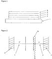
- FIG. 1 illustrates the structure of an OLED according to an embodiment of the invention.
- the OLED comprises a transparent glass or plastic substrate 1, an anode 2, a cathode 5, and a hole transporting layer 3 and a light-emitting layer 4 provided between anode 2 and the cathode 5.
- Further layers may be located between anode 2 and the cathode, such as charge transporting, charge injecting or charge blocking layers.
- an electron transporting layer may be provided between light-emitting layer 4 and cathode 5.
- holes are injected from the anode 2 and electrons are injected from cathode 5.
- the holes and electrons undergo recombination in a recombination zone 4a of the light emitting layer 4 to form excitons that undergo radiative decay.
- excitons that are formed by recombination of holes and electrons undergo radiative decay, and these excitons may be detrimental to device lifetime.
- singlet or triplet excitons may migrate from light emitting layer 4 into hole transport layer 3.
- excitons may be formed from electrons that pass through the light-emitting layer 4 and reach the hole transport layer. These excitons may interact with the material or materials of hole transport layer 3. The present inventors have identified that this interaction may reduce operational lifetime and/or efficiency of the device.
- Exciton migration from the light-emitting layer may occur if recombination zone 4a is close to the interface between the hole transport layer 3. Moreover, triplet excitons are typically relatively long-lived species and as such may migrate into hole transport layer 3 even if the recombination zone 4a is relatively distant from the interface between hole transport layer 3 and light emitting layer 4.
- Figure 2 illustrates an OLED having a hole transport layer into which excitons may migrate from the light emitting layer. If an electron transporting layer is present between the light emitting layer and cathode of an OLED (in which a hole transport layer may or may not be present) then it will be appreciated that excitons could equally migrate into the electron transporting layer with the similar detrimental effects. Likewise, holes reaching the electron transport layer could recombine with electrons to form excitons in the electron transporting layer.
- the present inventors have found that device lifetime may be improved. Without wishing to be bound by any theory, it is believed that the improvement in lifetime is attributable to absorption of excitons in the hole transport layer by the light-emitting dopant, which then allows the exciton to release its energy in the form of light.
- a number of measures may be taken to minimise the effect of the colour of light emitted from the charge transport layer on the colour of light emitted from the device, as compared to a control device in which no light-emitting dopant is present in the charge-transporting layer. These measures include but are not limited to:
- the charge-transporting layer comprises a charge-transporting polymer and a light-emitting dopant according to the claims.
- the charge-transporting polymer has an excited state energy level that is higher than an excited state energy level of the light-emitting dopant.
- the triplet excited state energy level (T 1 ) of the charge transporting polymer should be higher than that of the phosphorescent light-emitting dopant in order that triplet excitons may be transferred from the charge transporting polymer to the phosphorescent light-emitting dopant.
- the triplet level of the charge transporting polymer should be at least 0.01 eV higher than the triplet level of the phosphorescent dopant, more preferred 0.05 eV higher, even more preferred 0.1 eV or higher.
- the charge transporting polymer may be a conjugated or non-conjugated polymer, and charge transporting units may be provided in a polymer main-chain or polymer side-chain.
- a hole transporting layer preferably comprises a material having a low electron affinity (2 eV or lower) and low ionisation potential (5.8 eV or lower, preferably 5.7 eV or lower, more preferred 5.6 eV or lower). Electron affinities and ionisation potentials are typically measured by the methods disclosed in Shirota and Kageyama, Chem. Rev. 2007, 107, 953-1010 and references therein.
- a hole-transporting polymer may comprise arylamine repeat units, in particular repeat units of formula (V): wherein Ar 1 and Ar 2 in each occurrence are independently selected from optionally substituted aryl or heteroaryl groups, n is greater than or equal to 1, preferably 1 or 2, R is H or a substituent, preferably a substituent, and x and y are each independently 1, 2 or 3.
- R is preferably alkyl, Ar 3 , or a branched or linear chain of Ar 3 groups, for example -(Ar 3 ) r , wherein Ar 3 in each occurrence is independently selected from aryl or heteroaryl and r is at least 1, optionally 1, 2 or 3.
- Ar 1 , Ar 2 and Ar 3 may independently be substituted with one or more substituents.
- Preferred substituents are selected from the group R 3 consisting of:
- R may comprise a crosslinkable-group, for example a group comprising a polymerisable double bond such and a vinyl or acrylate group, or a benzocyclobutane group.
- any of the aryl or heteroaryl groups in the repeat unit of Formula (V) may be linked by a direct bond or a divalent linking atom or group.
- Preferred divalent linking atoms and groups include O, S; substituted N; and substituted C.
- substituted N or substituted C of R 3 , R 4 or of the divalent linking group may independently in each occurrence be NR 6 or CR 6 2 respectively wherein R 6 is alkyl or optionally substituted aryl or heteroaryl.
- Optional substituents for aryl or heteroaryl groups R 6 may be selected from R 4 or R 5 .
- R is Ar 3 and each of Ar 1 , Ar 2 and Ar 3 are independently and optionally substituted with one or more C 1-20 alkyl groups.
- Particularly preferred units satisfying Formula 1 include units of Formulae 1-3: wherein Ar 1 and Ar 2 are as defined above; and Ar 3 is optionally substituted aryl or heteroaryl. Where present, preferred substituents for Ar 3 include substituents as described for Ar 1 and Ar 2 , in particular alkyl and alkoxy groups.
- Ar 1 , Ar 2 and Ar 3 are preferably phenyl, each of which may independently be substituted with one or more substituents as described above.
- aryl or heteroaryl groups of formula (V) are phenyl, each phenyl group being optionally substituted with one or more alkyl groups.
- Ar 1 and Ar 2 are phenyl, each of which may be substituted with one or more C 1-20 alkyl groups, and R is 3,5-diphenylbenzene wherein each phenyl may be substituted with one or more alkyl groups.
- Ar 1 , Ar 2 and Ar 3 are each phenyl and are each optionally substituted with one or more alkyl groups, in particular C 1-20 alkyl.
- Specific hole transporting units include the following: wherein R 7 in each occurrence is independently H or a substituent, for example H or R 3 .
- Exemplary bipolar groups include the following: wherein R 7 is as described above.
- This polymer may be a homopolymer or it may be a copolymer comprising repeat units of formula (V) in an amount up to 99 mol %, preferably up to 70 mol %, even more preferred up to 50 mol%. These percentages apply to the total number of arylamine units present in the polymer in the case where more than one type of repeat unit of formula (V) is used.
- suitable co-polymers include co-polymers comprising a repeat unit of formula (V) and an arylene or heteroarylene co-repeat unit.
- exemplary arylene repeat units are disclosed in for example, Adv. Mater. 2000 12(23) 1737-1750 and include: 1,4-phenylene repeat units as disclosed in J. Appl. Phys. 1996, 79, 934 ; fluorene repeat units as disclosed in EP 0842208 ; indenofluorene repeat units as disclosed in, for example, Macromolecules 2000, 33(6), 2016-2020 ; and spirofluorene repeat units as disclosed in, for example EP 0707020 .
- Each of these repeat units is optionally substituted.
- substituents include solubilising groups such as C 1-20 alkyl or alkoxy; electron withdrawing groups such as fluorine, nitro or cyano; and substituents for increasing glass transition temperature (Tg) of the polymer.
- Particularly preferred arylene repeat units comprise optionally substituted, 2,7-linked fluorenes, most preferably repeat units of formula IV: wherein R 1 and R 2 are independently H or a substituent and wherein R 1 and R 2 may be linked to form a ring.
- R 1 and R 2 comprises an optionally substituted alky, e.g. C 1 -C 20 alkyl, or aryl, in particular phenyl, group.
- R 1 and R 2 may each independently comprise a linear or branched chain of aryl or heteroaryl groups, each of which groups may independently be substituted, for example a group of formula (Ar 3 ) r as described above.
- R 1 or R 2 comprises aryl or heteroaryl
- R 1 and / or R 2 may comprise a crosslinkable-group, for example a group comprising a polymerisable double bond such and a vinyl or acrylate group, or a benzocyclobutane group.
- Aryl(ene) and “heteroaryl(ene)” as used herein includes both fused and unfused aryl and heteroaryl groups respectively.
- a preferred arylene repeat unit is optionally substituted phenylene repeat units, such as 1,4-phenylene.
- the phenylene repeat unit may be substituted with one or more groups R 1 as described above, wherein each R 1 is independently in each occurrence H or a substituent, for example alkyl, for example repeat units of the formula (VII): wherein R 1 and R 2 are the same or different and are as described above with reference to the repeat unit of formula (IV).
- Preferred methods for preparation of conjugated charge-transporting polymers comprise a "metal insertion" wherein the metal atom of a metal complex catalyst is inserted between an aryl or heteroaryl group and a leaving group of a monomer.
- Exemplary metal insertion methods are Suzuki polymerisation as described in, for example, WO 00/53656 and Yamamoto polymerisation as described in, for example, T. Yamamoto, "Electrically Conducting And Thermally Stable ⁇ - Conjugated Poly(arylene)s Prepared by Organometallic Processes", Progress in Polymer Science 1993, 17, 1153-1205 .
- Yamamoto polymerisation a nickel complex catalyst is used; in the case of Suzuki polymerisation, a palladium complex catalyst is used.
- a monomer having two reactive halogen groups is used.
- at least one reactive group is a boron derivative group such as a boronic acid or boronic ester and the other reactive group is a halogen.
- Preferred halogens are chlorine, bromine and iodine, most preferably bromine.
- repeat units illustrated throughout this application may be derived from a monomer carrying suitable leaving groups.
- an end group or side group may be bound to the polymer by reaction of a suitable leaving group.
- Suzuki polymerisation may be used to prepare regioregular, block and random copolymers.
- homopolymers or random copolymers may be prepared when one reactive group is a halogen and the other reactive group is a boron derivative group.
- block or regioregular, in particular AB, copolymers may be prepared when both reactive groups of a first monomer are boron and both reactive groups of a second monomer are halogen.
- other leaving groups capable of participating in metal insertion include groups include tosylate, mesylate and triflate.
- An electron transporting layer preferably comprises a material having a high electron affinity (1.8 eV or higher, preferably 2 eV or higher, even more preferred 2.2 eV or higher) and high ionisation potential (5.8 eV or higher)
- Suitable electron transport groups include groups disclosed in, for example, Shirota and Kageyama, Chem. Rev. 2007, 107, 953-1010 .
- Electron transporting repeat units include groups comprise formula (II): -(Ar 1 ) r -Het-(Ar 2 ) r - (II) wherein Ar 1 and Ar 2 are as defined above; r is at least 1, preferably 1-3, and Het represents an optionally substituted heteroaryl group with high electron affinity .
- Optional substituents for Het are as described with respect to R above. In the case where Het is substituted with an aryl or heteroaryl group, this may be a group -(Ar 3 )r as described above.
- Suitable heteroaryls with high electron affinity include triazine, pyrimidine, oxadiazole, pyridine, triazole, triarylborane, sulfoxide and silole, in particular triphenyltriazine substituted with one or more substituent groups, for example triphenyl triazine substituted with one or more C 1-20 alkyl groups.
- Exemplary electron-transporting groups include the following: wherein R 7 is as described above.
- Suitable electron transport materials include optionally substituted ketones, diarylsulfoxides, and phosphine oxides. wherein R 7 is as described above.
- Suitable electron transport materials include optionally substituted boranes, for example Wherein R 7 is as described above.
- Certain groups may function as both hole- and electron-transporting groups. These are so-called ambipolar groups and include carbazoles, in particular groups of formulae 1, 2 or 3 in which two of Ar 1 , Ar 2 and Ar 3 are phenyl groups linked by a direct C-C bond. Ambipolar groups typically have an electron affinity around 2 eV and ionisation potential around 5.8 eV. Depending on its electron affinity and ionisation potential, the charge transporting layer may both transport one of holes and electrons and block the other of holes and electrons.
- Materials that may be used as phosphorescent light-emitting dopants according to the claims in the charge-transporting layer include metal complexes comprising optionally substituted complexes of formula (III): ML 1 q L 2 r L 3 s (III) wherein M is a metal; each of L 1 L 2 and L 3 is a coordinating group; q is an integer; r and s are each independently 0 or an integer; and the sum of (a. q) + (b. r) + (c.s) is equal to the number of coordination sites available on M, wherein a is the number of coordination sites on L 1 , b is the number of coordination sites on L 2 and c is the number of coordination sites on T 3
- Heavy elements M induce strong spin-orbit coupling to allow rapid intersystem crossing and emission from triplet or higher states (phosphorescence).
- Suitable heavy metals M include:
- Suitable coordinating groups for the f-block metals include oxygen or nitrogen donor systems such as carboxylic acids, 1,3-diketonates, hydroxy carboxylic acids, Schiff bases including acyl phenols and iminoacyl groups.
- oxygen or nitrogen donor systems such as carboxylic acids, 1,3-diketonates, hydroxy carboxylic acids, Schiff bases including acyl phenols and iminoacyl groups.
- luminescent lanthanide metal complexes require sensitizing group(s) which have the triplet excited energy level higher than the first excited state of the metal ion. Emission is from an f-f transition of the metal and so the emission colour is determined by the choice of the metal. The sharp emission is generally narrow, resulting in a pure colour emission useful for display applications.
- the d-block metals are particularly suitable for emission from triplet excited states. These metals form organometallic complexes with carbon or nitrogen donors such as porphyrin or bidentate ligands of formula (IV): wherein Ar 4 and Ar 5 may be the same or different and are independently selected from optionally substituted aryl or heteroaryl; X 1 and Y 1 may be the same or different and are independently selected from carbon or nitrogen; and Ar 4 and Ar 5 may be fused together.
- Ligands wherein X 1 is carbon and Y 1 is nitrogen are particularly preferred.
- Each of Ar 4 and Ar 5 may carry one or more substituents. Two or more of these substituents may be linked to form a ring, for example an aromatic ring.
- Particularly preferred substituents include fluorine or trifluoromethyl which may be used to blue-shift the emission of the complex as disclosed in WO 02/45466 , WO 02/44189 , US 2002-117662 and US 2002-182441 ; alkyl or alkoxy groups as disclosed in JP 2002-324679 ; carbazole which may be used to assist hole transport to the complex when used as an emissive material as disclosed in WO 02/81448 ; bromine, chlorine or iodine which can serve to functionalise the ligand for attachment of further groups as disclosed in WO 02/68435 and EP 1245659 ; and dendrons which may be used to obtain or enhance solution processability of the metal complex as disclosed in WO 02/66552 .
- a light-emitting dendrimer typically comprises a light-emitting core bound to one or more dendrons, wherein each dendron comprises a branching point and two or more dendritic branches.
- the dendron is at least partially conjugated, and at least one of the core and dendritic branches comprises an aryl or heteroaryl group.
- ligands suitable for use with d-block elements include diketonates, in particular acetylacetonate (acac); triarylphosphines and pyridine, each of which may be substituted.
- Main group metal complexes show ligand based, or charge transfer emission. For these complexes, the emission colour is determined by the choice of ligand as well as the metal.
- the charge transporting layer may contain one or more light-emitting dopants.
- the light-emitting dopant is chemically bound as a substituent attached to the polymer backbone of the charge transporting polymer, incorporated as a repeat unit in the polymer backbone or provided as an end-group of the polymer as disclosed in, for example, EP 1245659 , WO 02/31896 , WO 03/18653 and WO 03/22908 .
- This binding may result in more efficient transfer of excitons from the charge transporting materials to the light emitting dopant because it may provide intramolecular exciton transfer pathways unavailable to a corresponding mixed system.
- binding may be beneficial for processing reasons. For example, if the light emitting dopant has low solubility then binding it to a soluble charge transporting polymer allows the light emitting dopant to be carried in solution by the charge transporting polymer, enabling device fabrication using solution processing techniques. Furthermore, binding the light emitting dopant to the charge transporting polymer may prevent phase separation effects in solution-processed devices that may be detrimental to device performance.
- the charge transporting layer is optionally at least 10 nm thick, optionally at least 15 nm thick, optionally at least 20 nm thick.
- Suitable light-emitting materials for use in the light-emitting layer include small molecule, polymeric and dendrimeric materials, and compositions thereof.
- Suitable light-emitting polymers for use in layer 3 include poly(arylene vinylenes) such as poly(p-phenylene vinylenes) and polyarylenes such as: polyfluorenes, particularly 2,7-linked 9,9 dialkyl polyfluorenes or 2,7-linked 9,9 diaryl polyfluorenes; polyspirofluorenes, particularly 2,7-linked poly-9,9-spirofluorene; polyindenofluorenes, particularly 2,7-linked polyindenofluorenes; polyphenylenes, particularly alkyl or alkoxy substituted poly-1,4-phenylene.
- polymers as disclosed in, for example, Adv. Mater. 2000 12(23) 1737-1750 and references therein.
- Polymers for use as light-emitting materials in devices according to the present invention preferably comprise a repeat unit selected from optionally substituted arylene repeat units as described above, in particular phenylene repeat units such as repeat units of formula (VII) described above, and / or fluorene repeat units of formula (IV) described above.
- a light-emitting polymer in particular a fluorescent blue light-emitting polymer, may comprise an arylene or heteroarylene repeat unit as described above and an arylamine repeat unit, in particular a repeat unit of formula (V) as described above.
- the light-emitting layer may consist of a light-emitting material alone, or may comprise this material in combination with one or more further materials.
- the light-emitting polymer may be blended with hole and / or electron transporting materials or alternatively may be covalently bound to hole and / or electron transporting materials as disclosed in for example, WO 99/48160 .
- Exemplary hole and / or electron transporting materials may be selected from materials described above in relation to the charge-transporting layer.
- Light-emitting copolymers may comprise a light-emitting region and at least one of a hole transporting region and an electron transporting region as disclosed in, for example, WO 00/55927 and US 6353083 . If only one of a hole transporting region and electron transporting region is provided then the electroluminescent region may also provide the other of hole transport and electron transport functionality - for example, an amine unit as described above may provide both hole transport and light-emission functionality.
- a light-emitting copolymer comprising light-emitting repeat units and one or both of a hole transporting repeat units and electron transporting repeat units may provide said units in a polymer main-chain, as per US 6353083 , or in polymer side-groups pendant from the polymer backbone.
- the light emitting layer may comprise a host material and at least one light-emitting dopant.
- the host material may be a material as described above that would, in the absence of a dopant, emit light itself. When a host material and dopant are used in a device, the dopant alone may emit light. Alternatively, the host material and one or more dopants may emit light. White light may be generated by emission from multiple light sources, such as emission from both the host and one or more dopants or emission from multiple dopants.
- the light-emitting dopant may be selected from dopants as described above with respect to dopants present in the charge transporting layer.
- the singlet excited state energy level (S 1 ) of the host material should be higher than that of the fluorescent light-emitting dopant in order that singlet excitons may be transferred from the host material to the fluorescent light-emitting dopant.
- the singlet level of the host material should be at least 0.01 eV higher than the singlet level of the light-emitting dopant, more preferred 0.05 eV higher, even more preferred 0.1 eV or higher.
- the triplet excited state energy level (T 1 ) of the host material should be higher than that of the phosphorescent light-emitting dopant in order that triplet excitons may be transferred from the host material to the fluorescent light-emitting dopant.
- the triplet level of the host material should be at least 0.01 eV higher than the triplet level of the phosphorescent light-emitting dopant, more preferred 0.05 eV higher, even more preferred 0.1 eV or higher.
- the light-emitting dopant may be physically mixed with the host material or it may be chemically bound to the host material in the same manner described above with respect to binding of the light-emitting dopant to the charge transporting material.
- the light-emitting layer may be patterned or unpatterned.
- a device comprising an unpatterned layer may be used an illumination source, for example.
- a white light emitting device is particularly suitable for this purpose.
- a device comprising a patterned layer may be, for example, an active matrix display or a passive matrix display. In the case of an active matrix display, a patterned electroluminescent layer is typically used in combination with a patterned anode layer and an unpatterned cathode.
- the anode layer is formed of parallel stripes of anode material, and parallel stripes of electroluminescent material and cathode material arranged perpendicular to the anode material wherein the stripes of electroluminescent material and cathode material are typically separated by stripes of insulating material ("cathode separators") formed by photolithography.
- a conductive hole injection layer which may be formed from a conductive organic or inorganic material, may be provided between the anode and the light-emitting layer to assist hole injection from the anode into the layer or layers of semiconducting polymer.
- doped organic hole injection materials include optionally substituted, doped poly(ethylene dioxythiophene) (PEDT), in particular PEDT doped with a charge-balancing polyacid such as polystyrene sulfonate (PSS) as disclosed in EP 0901176 and EP 0947123 , polyacrylic acid or a fluorinated sulfonic acid, for example Nafion®; polyaniline as disclosed in US 5723873 and US 5798170 ; and optionally substituted polythiophene or poly(thienothiophene).
- conductive inorganic materials include transition metal oxides such as VOx MoOx and RuOx as disclosed in Journal of Physics D: Applied Physics (1996), 29(11), 2750-2753 .
- the cathode is selected from materials that have a workfunction allowing injection of electrons into the electroluminescent layer. Other factors influence the selection of the cathode such as the possibility of adverse interactions between the cathode and the light-emitting material of the light-emitting layer, in particular if the cathode and light-emitting layer are in direct contact.
- the cathode may consist of a single material such as a layer of aluminium. Alternatively, it may comprise a plurality of metals, for example a bilayer of a low workfunction material and a high workfunction material such as calcium and aluminium as disclosed in WO 98/10621 ; elemental barium as disclosed in WO 98/57381 , Appl. Phys. Lett.
- the cathode preferably has a workfunction of less than 3.5 eV, more preferably less than 3.2 eV, most preferably less than 3 eV. Work functions of metals can be found in, for example, Michaelson, J. Appl. Phys. 48(11), 4729, 1977 .
- the cathode may be opaque or transparent.
- Transparent cathodes are particularly advantageous for active matrix devices because emission through a transparent anode in such devices is at least partially blocked by drive circuitry located underneath the emissive pixels.
- a transparent cathode will comprises a layer of an electron injecting material that is sufficiently thin to be transparent. Typically, the lateral conductivity of this layer will be low as a result of its thinness. In this case, the layer of electron injecting material is used in combination with a thicker layer of transparent conducting material such as indium tin oxide.
- a transparent cathode device need not have a transparent anode (unless, of course, a fully transparent device is desired), and so the transparent anode used for bottom-emitting devices may be replaced or supplemented with a layer of reflective material such as a layer of aluminium.
- transparent cathode devices are disclosed in, for example, GB 2348316 .
- the substrate preferably has good barrier properties for prevention of ingress of moisture and oxygen into the device.
- the substrate is commonly glass, however alternative substrates may be used, in particular where flexibility of the device is desirable.
- the substrate may comprise a plastic as in US 6268695 which discloses a substrate of alternating plastic and barrier layers or a laminate of thin glass and plastic as disclosed in EP 0949850 .
- the device is preferably encapsulated with an encapsulant (not shown) to prevent ingress of moisture and oxygen.
- Suitable encapsulants include a sheet of glass, films having suitable barrier properties such as silicon dioxide, silicon monoxide, silicon nitride or alternating stacks of polymer and dielectric as disclosed in, for example, WO 01/81649 or an airtight container as disclosed in, for example, WO 01/19142 .
- a transparent cathode device a transparent encapsulating layer such as silicon monoxide or silicon dioxide may be deposited to micron levels of thickness, although in one preferred embodiment the thickness of such a layer is in the range of 20-300 nm.
- a getter material for absorption of any atmospheric moisture and / or oxygen that may permeate through the substrate or encapsulant may be disposed between the substrate and the encapsulant.
- the charge-transporting layer may be deposited from a solution in a solvent, and the light-emitting layer may be deposited by any process, including vacuum evaporation and deposition from a solution in a solvent.
- suitable solvents for solution deposition include mono- or poly-alkylbenzenes such as toluene and xylene.
- Particularly preferred solution deposition techniques including printing and coating techniques, preferably spin-coating and inkjet printing.
- Spin-coating is particularly suitable for devices wherein patterning of the light-emitting material is unnecessary - for example for lighting applications or simple monochrome segmented displays.
- Inkjet printing is particularly suitable for high information content displays, in particular full colour displays.
- a device may be inkjet printed by providing a patterned layer over the first electrode and defining wells for printing of one colour (in the case of a monochrome device) or multiple colours (in the case of a multicolour, in particular full colour device).
- the patterned layer is typically a layer of photoresist that is patterned to define wells as described in, for example, EP 0880303 .
- the ink may be printed into channels defined within a patterned layer.
- the photoresist may be patterned to form channels which, unlike wells, extend over a plurality of pixels and which may be closed or open at the channel ends.
- solution deposition techniques include dip-coating, roll printing and screen printing.
- adjacent charge transport layer and light-emitting layer are formed by solution processing then the skilled person will be aware of techniques to prevent intermixing of these layers, for example by crosslinking of one layer before deposition of the subsequent layer or selection of materials for adjacent layers such that the material from which the first of these layers is formed is not soluble in the solvent used to deposit the second layer.
- Hole transporting polymer was formed from the following monomers by Suzuki polymerisation as described in WO 00/53656 : Monomer Comparative hole transport polymer 1 (Mol %) Hole transport polymer 1 (Mol%) Hole transport polymer 2 (Mol%) Hole transport polymer 3 (Mol %) 50 50 50 12.5 10.5 12.25 11.5 30 30 30 30 7.5 7.5 7.5 2 0.25 1
- ITO ITO / HIL / HTL / EL / MF /Al / Ag
- ITO represents an indium-tin oxide anode
- HIL is a hole-injection layer formed from a hole injecting material obtained from Plextronics, Inc.
- HTL is a 15 nm thick hole transport layer of a polymer comprising hole transport polymer 1
- EL is electroluminescent layer formed to a thickness of 65 nmcontaining white Light-Emitting Polymer 1 illustrated below
- MF is a metal fluoride, and the trilayer of MF (2 nm) / Al (200 nm) / Ag (100 nm) forms a cathode for the device.
- HIL, HTL and EL were each formed by spin-coating followed by evaporation of the solvent. Following deposition of hole transporting polymer 1, the polymer layer was heated to crosslinking the benzocyclobutane groups of the polymer in order to render HTL insoluble prior to spin-coating of EL.
- Light-Emitting Polymer 1 was formed by Suzuki polymerisation of a polymerisation mixture comprising the molar percentages of monomers illustrated below. The polymerisation was carried out as described in WO 00/53656 , and the polymer was endcapped using the illustrated mono-brominated iridium complex to form a white light-emitting polymer.
- a device was prepared as per Example 1, except that hole transport layer 2 was used in place of hole transport layer 1.
- Devices 1 and 2 are not embodiments according to the claims.
- Comparative Device 1 was prepared as per Device 1, except that a non-emissive hole-transport layer was formed using comparative hole transport polymer 1 in place of hole transport layer 1.
- the CIE (x,y) co-ordinates and lifetime were measured.
- lifetime of the device was significantly increased by inclusion of fluorescent light-emitting species in the hole transport layer, without any significant change in colour of emission.
- inclusion of a fluorescent light-emitting species in the hole transporting layer provides a path for radiative decay of singlet excitons in the hole transporting layer.
- a device was prepared as per Device 1, except that the hole transport layer was formed from hole transporting polymer 3 and the light-emitting layer was formed from blue Light-Emitting Polymer 2, which was formed by Suzuki polymerisation of the following monomers:
- Comparative Device 2 was prepared as per Device 3 except that Comparative Hole Transport Polymer 1 was used in place of Hole Transporting Polymer 3.
- Device 3 is not an embodiment according to the claims.
- a device was prepared as per Device 1, except that the light-emitting layer was formed from blue Light-Emitting Polymer 3, which was formed by Suzuki polymerisation of the following monomers:
- Comparative Device 3 was prepared as per Device 4 except that Comparative Hole Transport Polymer 1 was used in place of Hole Transporting Polymer 1.
- Device 4 is not an embodiment according to the claims.
- a device was prepared as per Device 1, except that the light-emitting layer was formed from Light-Emitting Polymer 5 and the hole transport layer was formed to a thickness of 15 nm from hole transport polymer 4: Monomer Hole transport polymer 4 (mol %) Comparative hole transport polymer 4 (mol %) 50 50 41.8 42.5 7.5 7.5 0.7
- Comparative Device 5 was formed as described with reference to Example 5 except that non-emissive comparative hole transport polymer 4 was used in place of emissive hole transport polymer 4.
- a device was prepared as described in Example 5, except that the hole-transporting layer was formed to a thickness of 30 nm.
- Example CIE(x,y) co-ordinates and lifetime were measured.
- lifetime of the device was significantly increased by inclusion of a phosphorescent light-emitting species in the hole transport layer, without any significant change in colour of emission.
- inclusion of a phosphorescent light-emitting species in the hole transporting layer provides a path for radiative decay of triplet excitons in the hole transporting layer.
- a device was prepared as described in Example 5, except that the hole transporting layer was formed from hole transport polymer 5 (in Example 7) and hole transport polymer 6 (in Example 8), and the light-emitting layer was formed from a composition comprising host polymer 1 and light-emitting dopant 1 in a 70:30 w/w blend: Monomer Hole transport polymer 5 (mol %) Hole transport polymer 6 (mol%) Comparative hole transport polymer 5 (mol %) 50 50 42.5 42.5 42.5 7.45 7.25 7.5 0.1 0.5
- Comparative Example 7 was prepared as described above for Example 7, except that comparative hole transport polymer 5 was used in place of hole transport polymer 5.
- lifetime of the device was significantly increased by inclusion of a phosphorescent light-emitting species in the hole transport layer, without any significant change in colour of emission.
- inclusion of a phosphorescent light-emitting species in the hole transporting layer provides a path for radiative decay of triplet excitons in the hole transporting layer.
Claims (15)
- Dispositif émetteur de lumière organique comprenant une anode (2) ;
une cathode (5) ;
une couche de transport de charge comprenant un polymère de transport de charge dopé avec un dopant phosphorescent émetteur de lumière entre l'anode (2) et la cathode (5) ;
le dispositif comprenant en outre une couche émettrice de lumière (4) entre l'anode (2) et la cathode (5), dans lequel :la valeur de coordonnée x et/ou la valeur de coordonnée y des coordonnées CIE(x,y) de la lumière émise à partir du dispositif n'est pas supérieure de plus de 0,05 à la valeur de coordonnée x ou y respective d'un dispositif témoin dans lequel la couche de transport de charge n'est pas dopée avec un dopant émetteur de lumière ; dans lequel la couche de transport de charge est adjacente à la couche émettrice de lumière (4) ;et dans lequel le dopant émetteur de lumière est un motif de répétition dans la chaîne principale du polymère de transport de charge ou d'un groupe latéral ou d'un groupe d'extrémité du polymère de transport de charge ; caractérisé en ce que le dopant phosphorescent est présent dans la couche de transport de charge dans une quantité de pas plus de 0,75 mol %. - Dispositif émetteur de lumière organique selon la revendication 1 dans lequel la couche de transport de charge est une couche de transport de trous située entre l'anode et la couche émettrice de lumière.
- Dispositif émetteur de lumière organique selon la revendication 1 ou 2 dans lequel le dopant émetteur de lumière est un groupe d'extrémité du polymère de transport de charge.
- Dispositif émetteur de lumière organique selon l'une quelconque des revendications précédentes dans lequel la couche émettrice de lumière comprend un matériau hôte et un dopant émetteur de lumière qui est mélangé avec le matériau hôte ou lié chimiquement au matériau hôte.
- Dispositif émetteur de lumière organique selon la revendication 4 dans lequel le matériau hôte est un polymère.
- Dispositif émetteur de lumière organique selon la revendication 5 dans lequel le matériau hôte comprend des motifs de répétition arylamine.
- Dispositif émetteur de lumière organique selon l'une quelconque des revendications précédentes dans lequel le polymère de transport de charge comprend des motifs de répétition arylamine.
- Dispositif émetteur de lumière organique selon la revendication 6 ou 7 dans lequel les motifs de répétition arylamine sont des motifs de formule (V) :

- Dispositif émetteur de lumière organique selon la revendication 8 dans lequel R est Ar3, dans lequel Ar3 est un groupe aromatique ou hétéroaromatique facultativement substitué, et dans lequel deux quelconques de Ar1, Ar2 et Ar3 peuvent être liés par une liaison directe ou un groupe de liaison divalent.
- Dispositif émetteur de lumière organique selon l'une quelconque des revendications précédentes dans lequel le polymère de transport de charge comprend des motifs de répétition aryle ou hétéroaryle.
- Dispositif émetteur de lumière organique selon la revendication 10 dans lequel le polymère de transport de charge comprend des motifs de répétition de formule (IV) :

- Dispositif émetteur de lumière organique selon la revendication 10 ou 11 dans lequel le polymère de transport de charge comprend des motifs de répétition de formule (VII) :

- Dispositif émetteur de lumière organique selon l'une quelconque des revendications 1 et 3 à 12 dans lequel la couche de transport de charge est une couche de transport d'électrons située entre la cathode et la couche émettrice de lumière.
- Procédé de formation d'un dispositif émetteur de lumière organique selon l'une quelconque des revendications précédentes comprenant les étapes de dépôt de la couche de transport de charge et de la couche émettrice de lumière sur l'une de l'anode et de la cathode et le dépôt de l'autre de l'anode et de la cathode sur la couche de transport de charge et la couche émettrice de lumière, dans lequel au moins l'une de la couche de transport de charge et de la couche émettrice de lumière est déposée à partir d'une solution dans un solvant.
- Procédé selon la revendication 14 dans lequel la première de la couche de transport de charge et de la couche émettrice de lumière à être déposée est réticulée suite au dépôt, et dans lequel l'autre de la couche de transport de charge et de la couche émettrice de lumière est déposée sur la couche déposée en premier à partir d'une solution dans un solvant.
Applications Claiming Priority (4)
| Application Number | Priority Date | Filing Date | Title |
|---|---|---|---|
| GBGB1017628.7A GB201017628D0 (en) | 2010-10-19 | 2010-10-19 | Polymer and light-emitting device |
| GB1017626.1A GB2484680B (en) | 2010-10-19 | 2010-10-19 | Polymer and organic light-emitting device |
| GB1100630.1A GB2485001A (en) | 2010-10-19 | 2011-01-14 | OLEDs |
| PCT/GB2011/001499 WO2012052713A1 (fr) | 2010-10-19 | 2011-10-18 | Dispositif électroluminescent organique et procédé associé |
Publications (2)
| Publication Number | Publication Date |
|---|---|
| EP2630675A1 EP2630675A1 (fr) | 2013-08-28 |
| EP2630675B1 true EP2630675B1 (fr) | 2019-09-11 |
Family
ID=44947125
Family Applications (1)
| Application Number | Title | Priority Date | Filing Date |
|---|---|---|---|
| EP11781577.9A Active EP2630675B1 (fr) | 2010-10-19 | 2011-10-18 | Dispositif électroluminescent organique et procédé associé |
Country Status (8)
| Country | Link |
|---|---|
| US (2) | US20130270535A1 (fr) |
| EP (1) | EP2630675B1 (fr) |
| JP (3) | JP5981926B2 (fr) |
| KR (2) | KR20130129950A (fr) |
| CN (2) | CN103180989B (fr) |
| DE (1) | DE112011103507T5 (fr) |
| GB (2) | GB2485001A (fr) |
| WO (2) | WO2012052704A2 (fr) |
Families Citing this family (26)
| Publication number | Priority date | Publication date | Assignee | Title |
|---|---|---|---|---|
| US9812647B2 (en) | 2010-06-25 | 2017-11-07 | Cambridge Display Technology, Ltd. | Organic light-emitting device and method |
| GB201203159D0 (en) | 2012-02-23 | 2012-04-11 | Smartkem Ltd | Organic semiconductor compositions |
| GB201207866D0 (en) * | 2012-05-04 | 2012-06-20 | Cambridge Display Tech Ltd | Organic light emitting device and method |
| JP6046389B2 (ja) * | 2012-06-20 | 2016-12-14 | 住友化学株式会社 | 有機エレクトロルミネッセンス素子 |
| GB201223283D0 (en) * | 2012-12-21 | 2013-02-06 | Cambridge Display Tech Ltd | Polymer and organic electronic device |
| GB2514818B (en) | 2013-06-05 | 2015-12-16 | Cambridge Display Tech Ltd | Polymer and organic electronic device |
| JP6519108B2 (ja) * | 2013-07-12 | 2019-05-29 | 住友化学株式会社 | 組成物およびそれを用いた発光素子 |
| EP3037398B1 (fr) | 2013-08-22 | 2021-03-10 | Sumitomo Chemical Company, Limited | Procédé de fabrication d'un composé chimique |
| DK3039728T3 (en) | 2013-08-28 | 2018-08-20 | Smartkem Ltd | POLYMERIC ORGANIC SEMICONDUCTOR COMPOSITIONS |
| JP6390114B2 (ja) * | 2014-02-14 | 2018-09-19 | セイコーエプソン株式会社 | 成膜用インク、吐出検査方法、吐出検査装置および発光素子の製造方法 |
| WO2016026122A1 (fr) | 2014-08-21 | 2016-02-25 | Dow Global Technologies Llc | Compositions dérivées de benzocyclobutènes, et dispositifs électroniques les contenant |
| WO2016028906A1 (fr) | 2014-08-21 | 2016-02-25 | Dow Global Technologies Llc | Compositions dérivées de benzoclobutènes à substitution oxygène pour dispositifs électroniques |
| WO2016026123A1 (fr) | 2014-08-21 | 2016-02-25 | Dow Global Technologies Llc | Compositions comprenant des benzocyclobutènes substitués par de l'oxygène et des diénophiles et dispositifs électroniques contenant celles-ci |
| GB2529668A (en) * | 2014-08-28 | 2016-03-02 | Cambridge Display Tech Ltd | Organic light-emitting composition, device and method |
| GB201418876D0 (en) * | 2014-10-23 | 2014-12-03 | Cambridge Display Tech Ltd | Organic light emitting device |
| GB2533268A (en) * | 2014-12-02 | 2016-06-22 | Cambridge Display Tech Ltd | Organic light-emitting device |
| CN104600203B (zh) * | 2014-12-26 | 2017-02-22 | 合肥京东方光电科技有限公司 | 发光层及其制备方法、有机电致发光器件、显示装置 |
| US11005044B2 (en) | 2015-10-06 | 2021-05-11 | Sumitomo Chemical Company, Limited | Light emitting device |
| CN105372725B (zh) * | 2015-12-04 | 2018-06-05 | 江苏日久光电股份有限公司 | 高透过型光学阻隔薄膜 |
| KR102642199B1 (ko) * | 2016-04-07 | 2024-03-05 | 삼성디스플레이 주식회사 | 유기 발광 소자 |
| JP6943241B2 (ja) | 2016-06-24 | 2021-09-29 | 住友化学株式会社 | 発光素子 |
| US11718580B2 (en) | 2019-05-08 | 2023-08-08 | Meta Platforms Technologies, Llc | Fluorene derivatized monomers and polymers for volume Bragg gratings |
| US11780819B2 (en) | 2019-11-27 | 2023-10-10 | Meta Platforms Technologies, Llc | Aromatic substituted alkane-core monomers and polymers thereof for volume Bragg gratings |
| US20210155585A1 (en) * | 2019-11-27 | 2021-05-27 | Facebook Technologies, Llc | Anthraquinone derivatized monomers and polymers for volume bragg gratings |
| CN111403615B (zh) * | 2020-03-27 | 2022-07-12 | 深圳市华星光电半导体显示技术有限公司 | 有机发光器件及其制备方法 |
| US11879024B1 (en) | 2020-07-14 | 2024-01-23 | Meta Platforms Technologies, Llc | Soft mold formulations for surface relief grating fabrication with imprinting lithography |
Citations (2)
| Publication number | Priority date | Publication date | Assignee | Title |
|---|---|---|---|---|
| US20070057630A1 (en) * | 2005-09-15 | 2007-03-15 | Fuji Photo Film Co., Ltd. | Organic electroluminescent element |
| US20080026250A1 (en) * | 2006-07-28 | 2008-01-31 | General Electric Company | Electronic devices comprising organic iridium compositions |
Family Cites Families (86)
| Publication number | Priority date | Publication date | Assignee | Title |
|---|---|---|---|---|
| US4539507A (en) | 1983-03-25 | 1985-09-03 | Eastman Kodak Company | Organic electroluminescent devices having improved power conversion efficiencies |
| GB8909011D0 (en) | 1989-04-20 | 1989-06-07 | Friend Richard H | Electroluminescent devices |
| US5150006A (en) | 1991-08-01 | 1992-09-22 | Eastman Kodak Company | Blue emitting internal junction organic electroluminescent device (II) |
| US5432014A (en) | 1991-11-28 | 1995-07-11 | Sanyo Electric Co., Ltd. | Organic electroluminescent element and a method for producing the same |
| JP3332491B2 (ja) * | 1993-08-27 | 2002-10-07 | 三洋電機株式会社 | 有機el素子 |
| US5723873A (en) | 1994-03-03 | 1998-03-03 | Yang; Yang | Bilayer composite electrodes for diodes |
| DE69526614T2 (de) | 1994-09-12 | 2002-09-19 | Motorola Inc | Lichtemittierende Vorrichtungen die Organometallische Komplexe enthalten. |
| DE4436773A1 (de) | 1994-10-14 | 1996-04-18 | Hoechst Ag | Konjugierte Polymere mit Spirozentren und ihre Verwendung als Elektrolumineszenzmaterialien |
| US6723811B1 (en) * | 1994-12-28 | 2004-04-20 | Cambridge Display Technology Ltd. | Polymers for use in optical device |
| JP3865406B2 (ja) | 1995-07-28 | 2007-01-10 | 住友化学株式会社 | 2,7−アリール−9−置換フルオレン及び9−置換フルオレンオリゴマー及びポリマー |
| US5798170A (en) | 1996-02-29 | 1998-08-25 | Uniax Corporation | Long operating life for polymer light-emitting diodes |
| JP3724589B2 (ja) | 1996-07-29 | 2005-12-07 | ケンブリッジ ディスプレイ テクノロジー リミテッド | エレクトロルミネセンス素子 |
| JP3786969B2 (ja) | 1996-09-04 | 2006-06-21 | ケンブリッジ ディスプレイ テクノロジー リミテッド | 改良されたカソードを備える有機発光デバイス |
| JP3899566B2 (ja) | 1996-11-25 | 2007-03-28 | セイコーエプソン株式会社 | 有機el表示装置の製造方法 |
| JP3744103B2 (ja) * | 1997-02-21 | 2006-02-08 | 双葉電子工業株式会社 | 有機エレクトロルミネッセンス素子 |
| US6452218B1 (en) | 1997-06-10 | 2002-09-17 | Uniax Corporation | Ultra-thin alkaline earth metals as stable electron-injecting electrodes for polymer light emitting diodes |
| US5998045A (en) * | 1997-07-03 | 1999-12-07 | International Business Machines Corporation | Polymeric light-emitting device |
| GB9718393D0 (en) | 1997-08-29 | 1997-11-05 | Cambridge Display Tech Ltd | Electroluminescent Device |
| GB9805476D0 (en) | 1998-03-13 | 1998-05-13 | Cambridge Display Tech Ltd | Electroluminescent devices |
| KR100697861B1 (ko) | 1998-03-13 | 2007-03-22 | 캠브리지 디스플레이 테크놀로지 리미티드 | 전장 발광 디바이스들 |
| GB2335884A (en) | 1998-04-02 | 1999-10-06 | Cambridge Display Tech Ltd | Flexible substrates for electronic or optoelectronic devices |
| JP3825725B2 (ja) * | 1998-05-19 | 2006-09-27 | 三洋電機株式会社 | 有機エレクトロルミネッセンス素子 |
| JP3370011B2 (ja) * | 1998-05-19 | 2003-01-27 | 三洋電機株式会社 | 有機エレクトロルミネッセンス素子 |
| US6268695B1 (en) | 1998-12-16 | 2001-07-31 | Battelle Memorial Institute | Environmental barrier material for organic light emitting device and method of making |
| JP4505146B2 (ja) | 1999-02-04 | 2010-07-21 | ダウ グローバル テクノロジーズ インコーポレイティド | フルオレンコポリマーおよびそれから作られる素子 |
| GB9903251D0 (en) | 1999-02-12 | 1999-04-07 | Cambridge Display Tech Ltd | Opto-electric devices |
| US6541909B1 (en) * | 1999-03-02 | 2003-04-01 | Nec Corporation | Organic electroluminescent device with doped transport layer(s) and production method |
| DE60035970T2 (de) | 1999-03-05 | 2008-05-15 | Cambridge Display Technology Ltd. | Polymerherstellung |
| GB2348316A (en) | 1999-03-26 | 2000-09-27 | Cambridge Display Tech Ltd | Organic opto-electronic device |
| US6310360B1 (en) * | 1999-07-21 | 2001-10-30 | The Trustees Of Princeton University | Intersystem crossing agents for efficient utilization of excitons in organic light emitting devices |
| WO2001019142A1 (fr) | 1999-09-03 | 2001-03-15 | Uniax Corporation | Encapsulation de dispositifs electroniques organiques |
| US6413645B1 (en) | 2000-04-20 | 2002-07-02 | Battelle Memorial Institute | Ultrabarrier substrates |
| KR100329571B1 (ko) * | 2000-03-27 | 2002-03-23 | 김순택 | 유기 전자 발광소자 |
| US6939624B2 (en) | 2000-08-11 | 2005-09-06 | Universal Display Corporation | Organometallic compounds and emission-shifting organic electrophosphorescence |
| IL154960A0 (en) | 2000-10-10 | 2003-10-31 | Du Pont | Polymers having attached luminescent metal complexes and devices made with sych polymers |
| KR100533556B1 (ko) | 2000-11-30 | 2005-12-06 | 캐논 가부시끼가이샤 | 발광 소자 및 표시 장치 |
| KR100825182B1 (ko) | 2000-11-30 | 2008-04-24 | 캐논 가부시끼가이샤 | 발광 소자 및 표시 장치 |
| US6693295B2 (en) | 2000-12-25 | 2004-02-17 | Fuji Photo Film Co., Ltd. | Indole derivative, material for light-emitting device and light-emitting device using the same |
| CA2438745C (fr) | 2001-02-20 | 2010-11-30 | Isis Innovation Limited | Dendrimeres contenant du metal |
| DE10109027A1 (de) | 2001-02-24 | 2002-09-05 | Covion Organic Semiconductors | Rhodium- und Iridium-Komplexe |
| JP4994564B2 (ja) * | 2001-03-02 | 2012-08-08 | ザ、トラスティーズ オブ プリンストン ユニバーシティ | 二重ドープ層燐光有機発光装置 |
| SG92833A1 (en) | 2001-03-27 | 2002-11-19 | Sumitomo Chemical Co | Polymeric light emitting substance and polymer light emitting device using the same |
| JP4048810B2 (ja) * | 2001-03-27 | 2008-02-20 | 住友化学株式会社 | 高分子発光体およびそれを用いた高分子発光素子 |
| KR20030087056A (ko) | 2001-04-05 | 2003-11-12 | 상꾜 가부시키가이샤 | 벤즈아미딘 유도체 |
| KR20030024690A (ko) | 2001-04-17 | 2003-03-26 | 코닌클리케 필립스 일렉트로닉스 엔.브이. | 저 황산염 및 고 금속 이온 함량을 갖는 전도성 투명중합체 층을 포함하는 led |
| JP2002324679A (ja) | 2001-04-26 | 2002-11-08 | Honda Motor Co Ltd | 有機エレクトロルミネッセンス素子 |
| US6565996B2 (en) * | 2001-06-06 | 2003-05-20 | Eastman Kodak Company | Organic light-emitting device having a color-neutral dopant in a hole-transport layer and/or in an electron-transport layer |
| JP4407102B2 (ja) | 2001-08-06 | 2010-02-03 | 三菱化学株式会社 | アントラセン系化合物、その製造方法および有機電界発光素子 |
| US6638644B2 (en) * | 2001-08-28 | 2003-10-28 | Eastman Kodak Company | Electroluminescent devices having diarylanthracene polymers |
| JP4574936B2 (ja) | 2001-08-31 | 2010-11-04 | 日本放送協会 | 燐光発光性化合物及び燐光発光性組成物 |
| JP4629643B2 (ja) * | 2001-08-31 | 2011-02-09 | 日本放送協会 | 有機発光素子及び表示装置 |
| US7250226B2 (en) * | 2001-08-31 | 2007-07-31 | Nippon Hoso Kyokai | Phosphorescent compound, a phosphorescent composition and an organic light-emitting device |
| EP1426399A4 (fr) | 2001-09-04 | 2005-07-13 | Canon Kk | Composes de poids moleculaire eleve et dispositifs luminescents organiques |
| JP2003073480A (ja) * | 2001-09-04 | 2003-03-12 | Canon Inc | 高分子化合物及び有機発光素子 |
| JP2003086376A (ja) * | 2001-09-06 | 2003-03-20 | Nippon Hoso Kyokai <Nhk> | 有機エレクトロルミネッセンスデバイスおよびその製造方法 |
| EP1513911A1 (fr) * | 2002-06-04 | 2005-03-16 | H.C. Starck GmbH | Polymeres conjugues phosphorescents et luminescents et leur utilisation dans des systemes electroluminescents |
| JP4258192B2 (ja) * | 2002-09-17 | 2009-04-30 | 富士ゼロックス株式会社 | 有機電界発光素子 |
| AU2003289392A1 (en) * | 2002-12-26 | 2004-07-22 | Semiconductor Energy Laboratory Co., Ltd. | Organic light emitting element |
| GB0306409D0 (en) * | 2003-03-20 | 2003-04-23 | Cambridge Display Tech Ltd | Electroluminescent device |
| JP4300902B2 (ja) * | 2003-06-23 | 2009-07-22 | コニカミノルタホールディングス株式会社 | ブロック共重合体、有機エレクトロルミネッセンス素子、表示装置、照明装置及び光源 |
| EP1644460B1 (fr) * | 2003-07-10 | 2008-01-30 | MERCK PATENT GmbH | Anthracenes substitues |
| JP4650265B2 (ja) * | 2003-07-23 | 2011-03-16 | コニカミノルタホールディングス株式会社 | 有機エレクトロルミネッセンス素子、照明装置及び表示装置 |
| JP2005108746A (ja) * | 2003-10-01 | 2005-04-21 | Internatl Business Mach Corp <Ibm> | 有機エレクトロ・ルミネッセンス素子および有機エレクトロ・ルミネッセンス素子の製造方法 |
| WO2005049689A2 (fr) | 2003-11-17 | 2005-06-02 | Sumitomo Chemical Company, Limited | Composes reticulables substitues de fluorene et oligomères et polymeres conjugues en etant faits |
| GB0329364D0 (en) * | 2003-12-19 | 2004-01-21 | Cambridge Display Tech Ltd | Optical device |
| US7267892B2 (en) * | 2004-02-25 | 2007-09-11 | Eastman Kodak Company | Electroluminescent devices having pendant naphthylanthracene-based polymers |
| GB2433509A (en) * | 2005-12-22 | 2007-06-27 | Cambridge Display Tech Ltd | Arylamine polymer |
| US7645525B2 (en) * | 2005-12-27 | 2010-01-12 | Lg Display Co., Ltd. | Organic light emitting devices |
| JP2007201190A (ja) * | 2006-01-26 | 2007-08-09 | Fuji Xerox Co Ltd | 有機電界発光素子 |
| JP2007317966A (ja) * | 2006-05-26 | 2007-12-06 | Fuji Xerox Co Ltd | 有機電界発光素子およびその製造方法、並びに画像表示媒体 |
| JP5144938B2 (ja) * | 2007-02-02 | 2013-02-13 | 住友化学株式会社 | 高分子発光素子、高分子化合物、組成物、液状組成物及び導電性薄膜 |
| JP5326417B2 (ja) * | 2007-10-18 | 2013-10-30 | 三菱化学株式会社 | 電荷輸送膜及び有機電界発光素子 |
| EP2203944B1 (fr) * | 2007-10-24 | 2014-04-16 | Merck Patent GmbH | Dispositif optoelectronique |
| US20110037058A1 (en) * | 2007-10-24 | 2011-02-17 | Merck Patent Gmbh Patents & Scientific Information | Optoelectronic device |
| KR20100092009A (ko) * | 2007-12-11 | 2010-08-19 | 이데미쓰 고산 가부시키가이샤 | 고분자 화합물 및 그것을 사용한 유기 전기발광 소자 |
| JP5434088B2 (ja) * | 2008-01-22 | 2014-03-05 | 三菱化学株式会社 | 架橋性有機化合物、有機電界発光素子用組成物、有機電界発光素子および有機elディスプレイ |
| GB2456788B (en) * | 2008-01-23 | 2011-03-09 | Cambridge Display Tech Ltd | White light emitting material |
| CN101981086A (zh) * | 2008-04-02 | 2011-02-23 | 三菱化学株式会社 | 高分子化合物、由该高分子化合物交联而得到的网状高分子化合物、有机场致发光元件用组合物、有机场致发光元件、有机el显示器及有机el照明 |
| GB0814161D0 (en) * | 2008-08-01 | 2008-09-10 | Cambridge Display Tech Ltd | Blue-light emitting material |
| JP5491796B2 (ja) * | 2008-08-11 | 2014-05-14 | 三菱化学株式会社 | 電荷輸送性ポリマー、有機電界発光素子用組成物、有機電界発光素子、有機elディスプレイ及び有機el照明 |
| EP2344928A1 (fr) * | 2008-09-09 | 2011-07-20 | Merck Patent GmbH | Matière organique et dispositif électrophotographique |
| JP2010225563A (ja) * | 2009-03-25 | 2010-10-07 | Panasonic Electric Works Co Ltd | 有機el素子 |
| TWI469968B (zh) * | 2009-03-31 | 2015-01-21 | Semiconductor Energy Lab | 雜環化合物及使用該雜環化合物之發光元件、發光裝置、照明裝置和電子設備 |
| GB0906554D0 (en) * | 2009-04-16 | 2009-05-20 | Cambridge Display Tech Ltd | Organic electroluminescent device |
| JPWO2011071169A1 (ja) * | 2009-12-11 | 2013-04-22 | 三菱化学株式会社 | 有機電界発光素子、有機el表示装置及び有機el照明 |
| CN101759685B (zh) * | 2009-12-30 | 2013-09-04 | 黑龙江大学 | 一种有机电致发光铱配合物及其制备方法和应用 |
-
2011
- 2011-01-14 GB GB1100630.1A patent/GB2485001A/en not_active Withdrawn
- 2011-10-18 JP JP2013534373A patent/JP5981926B2/ja active Active
- 2011-10-18 KR KR1020137012877A patent/KR20130129950A/ko active Search and Examination
- 2011-10-18 CN CN201180050392.7A patent/CN103180989B/zh active Active
- 2011-10-18 US US13/880,234 patent/US20130270535A1/en not_active Abandoned
- 2011-10-18 WO PCT/GB2011/001488 patent/WO2012052704A2/fr active Application Filing
- 2011-10-18 KR KR1020137012863A patent/KR20130129949A/ko active Search and Examination
- 2011-10-18 US US13/880,242 patent/US20130299787A1/en not_active Abandoned
- 2011-10-18 GB GB1306731.9A patent/GB2497904A/en not_active Withdrawn
- 2011-10-18 WO PCT/GB2011/001499 patent/WO2012052713A1/fr active Application Filing
- 2011-10-18 JP JP2013534375A patent/JP5951619B2/ja active Active
- 2011-10-18 DE DE112011103507.1T patent/DE112011103507T5/de active Pending
- 2011-10-18 CN CN201180050761.2A patent/CN103180991B/zh active Active
- 2011-10-18 EP EP11781577.9A patent/EP2630675B1/fr active Active
-
2016
- 2016-06-08 JP JP2016114148A patent/JP6239692B2/ja active Active
Patent Citations (2)
| Publication number | Priority date | Publication date | Assignee | Title |
|---|---|---|---|---|
| US20070057630A1 (en) * | 2005-09-15 | 2007-03-15 | Fuji Photo Film Co., Ltd. | Organic electroluminescent element |
| US20080026250A1 (en) * | 2006-07-28 | 2008-01-31 | General Electric Company | Electronic devices comprising organic iridium compositions |
Also Published As
| Publication number | Publication date |
|---|---|
| CN103180991B (zh) | 2016-03-23 |
| WO2012052713A1 (fr) | 2012-04-26 |
| JP2013546173A (ja) | 2013-12-26 |
| US20130270535A1 (en) | 2013-10-17 |
| KR20130129949A (ko) | 2013-11-29 |
| WO2012052704A3 (fr) | 2012-06-07 |
| CN103180989A (zh) | 2013-06-26 |
| DE112011103507T5 (de) | 2014-01-16 |
| GB2497904A (en) | 2013-06-26 |
| GB201306731D0 (en) | 2013-05-29 |
| EP2630675A1 (fr) | 2013-08-28 |
| GB201100630D0 (en) | 2011-03-02 |
| CN103180989B (zh) | 2017-02-15 |
| JP6239692B2 (ja) | 2017-11-29 |
| KR20130129950A (ko) | 2013-11-29 |
| US20130299787A1 (en) | 2013-11-14 |
| GB2485001A (en) | 2012-05-02 |
| JP2014508394A (ja) | 2014-04-03 |
| JP2016192559A (ja) | 2016-11-10 |
| JP5951619B2 (ja) | 2016-07-13 |
| CN103180991A (zh) | 2013-06-26 |
| JP5981926B2 (ja) | 2016-08-31 |
| WO2012052704A2 (fr) | 2012-04-26 |
Similar Documents
| Publication | Publication Date | Title |
|---|---|---|
| EP2630675B1 (fr) | Dispositif électroluminescent organique et procédé associé | |
| US9493613B2 (en) | Organic light emitting composition, device and method | |
| US8981365B2 (en) | Organic light emissive device comprising a trilayer cathode including a layer comprising sodium fluoride | |
| US9761820B2 (en) | Polymer | |
| WO2011141714A1 (fr) | Polymère électroluminescent organique et dispositif | |
| WO2009066061A1 (fr) | Dispositif électroluminescent et matériaux utilisés pour ce dispositif | |
| US20130292657A1 (en) | Polymer and organic light-emitting device | |
| US9735370B2 (en) | Compound, device and method of making same | |
| EP1979958A1 (fr) | Dispositif electroluminescent organique phosphorescent | |
| GB2484680A (en) | Polymer and organic light-emitting device | |
| US20160372667A1 (en) | Light emitting composition and device | |
| WO2010001104A1 (fr) | Dispositif électronique organique | |
| WO2007129015A1 (fr) | Polymères et dispositifs opto-électriques | |
| EP1829129B1 (fr) | Dispositif luminescent | |
| GB2483628A (en) | Organic Light-Emitting Composition | |
| WO2010013002A1 (fr) | Matériaux et dispositifs électroluminescents organiques | |
| WO2015079261A1 (fr) | Dispositif électroluminescent polymère et organique | |
| US10403823B2 (en) | Polymer and organic light emitting device | |
| US20170309837A1 (en) | Polymer and organic light-emitting device |
Legal Events
| Date | Code | Title | Description |
|---|---|---|---|
| PUAI | Public reference made under article 153(3) epc to a published international application that has entered the european phase |
Free format text: ORIGINAL CODE: 0009012 |
|
| 17P | Request for examination filed |
Effective date: 20130412 |
|
| AK | Designated contracting states |
Kind code of ref document: A1 Designated state(s): AL AT BE BG CH CY CZ DE DK EE ES FI FR GB GR HR HU IE IS IT LI LT LU LV MC MK MT NL NO PL PT RO RS SE SI SK SM TR |
|
| DAX | Request for extension of the european patent (deleted) | ||
| RAP1 | Party data changed (applicant data changed or rights of an application transferred) |
Owner name: CAMBRIDGE DISPLAY TECHNOLOGY LIMITED Owner name: SUMITOMO CHEMICAL COMPANY LIMITED |
|
| 17Q | First examination report despatched |
Effective date: 20160229 |
|
| STAA | Information on the status of an ep patent application or granted ep patent |
Free format text: STATUS: EXAMINATION IS IN PROGRESS |
|
| REG | Reference to a national code |
Ref country code: DE Ref legal event code: R079 Ref document number: 602011062009 Country of ref document: DE Free format text: PREVIOUS MAIN CLASS: H01L0051000000 Ipc: H01L0051540000 |
|
| GRAP | Despatch of communication of intention to grant a patent |
Free format text: ORIGINAL CODE: EPIDOSNIGR1 |
|
| STAA | Information on the status of an ep patent application or granted ep patent |
Free format text: STATUS: GRANT OF PATENT IS INTENDED |
|
| RIC1 | Information provided on ipc code assigned before grant |
Ipc: H01L 51/54 20060101AFI20190307BHEP |
|
| INTG | Intention to grant announced |
Effective date: 20190325 |
|
| GRAS | Grant fee paid |
Free format text: ORIGINAL CODE: EPIDOSNIGR3 |
|
| GRAA | (expected) grant |
Free format text: ORIGINAL CODE: 0009210 |
|
| STAA | Information on the status of an ep patent application or granted ep patent |
Free format text: STATUS: THE PATENT HAS BEEN GRANTED |
|
| AK | Designated contracting states |
Kind code of ref document: B1 Designated state(s): AL AT BE BG CH CY CZ DE DK EE ES FI FR GB GR HR HU IE IS IT LI LT LU LV MC MK MT NL NO PL PT RO RS SE SI SK SM TR |
|
| REG | Reference to a national code |
Ref country code: GB Ref legal event code: FG4D |
|
| REG | Reference to a national code |
Ref country code: CH Ref legal event code: EP |
|
| REG | Reference to a national code |
Ref country code: AT Ref legal event code: REF Ref document number: 1179621 Country of ref document: AT Kind code of ref document: T Effective date: 20190915 |
|
| REG | Reference to a national code |
Ref country code: DE Ref legal event code: R096 Ref document number: 602011062009 Country of ref document: DE Ref country code: IE Ref legal event code: FG4D |
|
| REG | Reference to a national code |
Ref country code: NL Ref legal event code: MP Effective date: 20190911 |
|
| REG | Reference to a national code |
Ref country code: LT Ref legal event code: MG4D |
|
| PG25 | Lapsed in a contracting state [announced via postgrant information from national office to epo] |
Ref country code: FI Free format text: LAPSE BECAUSE OF FAILURE TO SUBMIT A TRANSLATION OF THE DESCRIPTION OR TO PAY THE FEE WITHIN THE PRESCRIBED TIME-LIMIT Effective date: 20190911 Ref country code: HR Free format text: LAPSE BECAUSE OF FAILURE TO SUBMIT A TRANSLATION OF THE DESCRIPTION OR TO PAY THE FEE WITHIN THE PRESCRIBED TIME-LIMIT Effective date: 20190911 Ref country code: LT Free format text: LAPSE BECAUSE OF FAILURE TO SUBMIT A TRANSLATION OF THE DESCRIPTION OR TO PAY THE FEE WITHIN THE PRESCRIBED TIME-LIMIT Effective date: 20190911 Ref country code: BG Free format text: LAPSE BECAUSE OF FAILURE TO SUBMIT A TRANSLATION OF THE DESCRIPTION OR TO PAY THE FEE WITHIN THE PRESCRIBED TIME-LIMIT Effective date: 20191211 Ref country code: SE Free format text: LAPSE BECAUSE OF FAILURE TO SUBMIT A TRANSLATION OF THE DESCRIPTION OR TO PAY THE FEE WITHIN THE PRESCRIBED TIME-LIMIT Effective date: 20190911 Ref country code: NO Free format text: LAPSE BECAUSE OF FAILURE TO SUBMIT A TRANSLATION OF THE DESCRIPTION OR TO PAY THE FEE WITHIN THE PRESCRIBED TIME-LIMIT Effective date: 20191211 |
|
| PG25 | Lapsed in a contracting state [announced via postgrant information from national office to epo] |
Ref country code: AL Free format text: LAPSE BECAUSE OF FAILURE TO SUBMIT A TRANSLATION OF THE DESCRIPTION OR TO PAY THE FEE WITHIN THE PRESCRIBED TIME-LIMIT Effective date: 20190911 Ref country code: RS Free format text: LAPSE BECAUSE OF FAILURE TO SUBMIT A TRANSLATION OF THE DESCRIPTION OR TO PAY THE FEE WITHIN THE PRESCRIBED TIME-LIMIT Effective date: 20190911 Ref country code: ES Free format text: LAPSE BECAUSE OF FAILURE TO SUBMIT A TRANSLATION OF THE DESCRIPTION OR TO PAY THE FEE WITHIN THE PRESCRIBED TIME-LIMIT Effective date: 20190911 Ref country code: LV Free format text: LAPSE BECAUSE OF FAILURE TO SUBMIT A TRANSLATION OF THE DESCRIPTION OR TO PAY THE FEE WITHIN THE PRESCRIBED TIME-LIMIT Effective date: 20190911 Ref country code: GR Free format text: LAPSE BECAUSE OF FAILURE TO SUBMIT A TRANSLATION OF THE DESCRIPTION OR TO PAY THE FEE WITHIN THE PRESCRIBED TIME-LIMIT Effective date: 20191212 |
|
| REG | Reference to a national code |
Ref country code: AT Ref legal event code: MK05 Ref document number: 1179621 Country of ref document: AT Kind code of ref document: T Effective date: 20190911 |
|
| PG25 | Lapsed in a contracting state [announced via postgrant information from national office to epo] |
Ref country code: IT Free format text: LAPSE BECAUSE OF FAILURE TO SUBMIT A TRANSLATION OF THE DESCRIPTION OR TO PAY THE FEE WITHIN THE PRESCRIBED TIME-LIMIT Effective date: 20190911 Ref country code: EE Free format text: LAPSE BECAUSE OF FAILURE TO SUBMIT A TRANSLATION OF THE DESCRIPTION OR TO PAY THE FEE WITHIN THE PRESCRIBED TIME-LIMIT Effective date: 20190911 Ref country code: PL Free format text: LAPSE BECAUSE OF FAILURE TO SUBMIT A TRANSLATION OF THE DESCRIPTION OR TO PAY THE FEE WITHIN THE PRESCRIBED TIME-LIMIT Effective date: 20190911 Ref country code: RO Free format text: LAPSE BECAUSE OF FAILURE TO SUBMIT A TRANSLATION OF THE DESCRIPTION OR TO PAY THE FEE WITHIN THE PRESCRIBED TIME-LIMIT Effective date: 20190911 Ref country code: AT Free format text: LAPSE BECAUSE OF FAILURE TO SUBMIT A TRANSLATION OF THE DESCRIPTION OR TO PAY THE FEE WITHIN THE PRESCRIBED TIME-LIMIT Effective date: 20190911 Ref country code: NL Free format text: LAPSE BECAUSE OF FAILURE TO SUBMIT A TRANSLATION OF THE DESCRIPTION OR TO PAY THE FEE WITHIN THE PRESCRIBED TIME-LIMIT Effective date: 20190911 Ref country code: PT Free format text: LAPSE BECAUSE OF FAILURE TO SUBMIT A TRANSLATION OF THE DESCRIPTION OR TO PAY THE FEE WITHIN THE PRESCRIBED TIME-LIMIT Effective date: 20200113 |
|
| PG25 | Lapsed in a contracting state [announced via postgrant information from national office to epo] |
Ref country code: CZ Free format text: LAPSE BECAUSE OF FAILURE TO SUBMIT A TRANSLATION OF THE DESCRIPTION OR TO PAY THE FEE WITHIN THE PRESCRIBED TIME-LIMIT Effective date: 20190911 Ref country code: SK Free format text: LAPSE BECAUSE OF FAILURE TO SUBMIT A TRANSLATION OF THE DESCRIPTION OR TO PAY THE FEE WITHIN THE PRESCRIBED TIME-LIMIT Effective date: 20190911 Ref country code: SM Free format text: LAPSE BECAUSE OF FAILURE TO SUBMIT A TRANSLATION OF THE DESCRIPTION OR TO PAY THE FEE WITHIN THE PRESCRIBED TIME-LIMIT Effective date: 20190911 Ref country code: IS Free format text: LAPSE BECAUSE OF FAILURE TO SUBMIT A TRANSLATION OF THE DESCRIPTION OR TO PAY THE FEE WITHIN THE PRESCRIBED TIME-LIMIT Effective date: 20200224 |
|
| REG | Reference to a national code |
Ref country code: CH Ref legal event code: PL |
|
| REG | Reference to a national code |
Ref country code: DE Ref legal event code: R097 Ref document number: 602011062009 Country of ref document: DE |
|
| PLBE | No opposition filed within time limit |
Free format text: ORIGINAL CODE: 0009261 |
|
| STAA | Information on the status of an ep patent application or granted ep patent |
Free format text: STATUS: NO OPPOSITION FILED WITHIN TIME LIMIT |
|
| PG2D | Information on lapse in contracting state deleted |
Ref country code: IS |
|
| PG25 | Lapsed in a contracting state [announced via postgrant information from national office to epo] |
Ref country code: IS Free format text: LAPSE BECAUSE OF FAILURE TO SUBMIT A TRANSLATION OF THE DESCRIPTION OR TO PAY THE FEE WITHIN THE PRESCRIBED TIME-LIMIT Effective date: 20200112 Ref country code: LU Free format text: LAPSE BECAUSE OF NON-PAYMENT OF DUE FEES Effective date: 20191018 Ref country code: DK Free format text: LAPSE BECAUSE OF FAILURE TO SUBMIT A TRANSLATION OF THE DESCRIPTION OR TO PAY THE FEE WITHIN THE PRESCRIBED TIME-LIMIT Effective date: 20190911 Ref country code: LI Free format text: LAPSE BECAUSE OF NON-PAYMENT OF DUE FEES Effective date: 20191031 Ref country code: CH Free format text: LAPSE BECAUSE OF NON-PAYMENT OF DUE FEES Effective date: 20191031 |
|
| REG | Reference to a national code |
Ref country code: BE Ref legal event code: MM Effective date: 20191031 |
|
| 26N | No opposition filed |
Effective date: 20200615 |
|
| PG25 | Lapsed in a contracting state [announced via postgrant information from national office to epo] |
Ref country code: SI Free format text: LAPSE BECAUSE OF FAILURE TO SUBMIT A TRANSLATION OF THE DESCRIPTION OR TO PAY THE FEE WITHIN THE PRESCRIBED TIME-LIMIT Effective date: 20190911 Ref country code: MC Free format text: LAPSE BECAUSE OF FAILURE TO SUBMIT A TRANSLATION OF THE DESCRIPTION OR TO PAY THE FEE WITHIN THE PRESCRIBED TIME-LIMIT Effective date: 20190911 Ref country code: BE Free format text: LAPSE BECAUSE OF NON-PAYMENT OF DUE FEES Effective date: 20191031 |
|
| GBPC | Gb: european patent ceased through non-payment of renewal fee |
Effective date: 20191211 |
|
| REG | Reference to a national code |
Ref country code: DE Ref legal event code: R082 Ref document number: 602011062009 Country of ref document: DE Representative=s name: VENNER SHIPLEY GERMANY LLP, DE Ref country code: DE Ref legal event code: R082 Ref document number: 602011062009 Country of ref document: DE Representative=s name: VENNER SHIPLEY LLP, DE |
|
| PG25 | Lapsed in a contracting state [announced via postgrant information from national office to epo] |
Ref country code: IE Free format text: LAPSE BECAUSE OF NON-PAYMENT OF DUE FEES Effective date: 20191018 Ref country code: GB Free format text: LAPSE BECAUSE OF NON-PAYMENT OF DUE FEES Effective date: 20191211 |
|
| PG25 | Lapsed in a contracting state [announced via postgrant information from national office to epo] |
Ref country code: CY Free format text: LAPSE BECAUSE OF FAILURE TO SUBMIT A TRANSLATION OF THE DESCRIPTION OR TO PAY THE FEE WITHIN THE PRESCRIBED TIME-LIMIT Effective date: 20190911 |
|
| PG25 | Lapsed in a contracting state [announced via postgrant information from national office to epo] |
Ref country code: HU Free format text: LAPSE BECAUSE OF FAILURE TO SUBMIT A TRANSLATION OF THE DESCRIPTION OR TO PAY THE FEE WITHIN THE PRESCRIBED TIME-LIMIT; INVALID AB INITIO Effective date: 20111018 Ref country code: MT Free format text: LAPSE BECAUSE OF FAILURE TO SUBMIT A TRANSLATION OF THE DESCRIPTION OR TO PAY THE FEE WITHIN THE PRESCRIBED TIME-LIMIT Effective date: 20190911 Ref country code: FR Free format text: LAPSE BECAUSE OF NON-PAYMENT OF DUE FEES Effective date: 20191112 |
|
| PG25 | Lapsed in a contracting state [announced via postgrant information from national office to epo] |
Ref country code: TR Free format text: LAPSE BECAUSE OF FAILURE TO SUBMIT A TRANSLATION OF THE DESCRIPTION OR TO PAY THE FEE WITHIN THE PRESCRIBED TIME-LIMIT Effective date: 20190911 |
|
| PG25 | Lapsed in a contracting state [announced via postgrant information from national office to epo] |
Ref country code: MK Free format text: LAPSE BECAUSE OF FAILURE TO SUBMIT A TRANSLATION OF THE DESCRIPTION OR TO PAY THE FEE WITHIN THE PRESCRIBED TIME-LIMIT Effective date: 20190911 |
|
| REG | Reference to a national code |
Ref country code: DE Ref legal event code: R079 Ref document number: 602011062009 Country of ref document: DE Free format text: PREVIOUS MAIN CLASS: H01L0051540000 Ipc: H10K0085000000 |
|
| P01 | Opt-out of the competence of the unified patent court (upc) registered |
Effective date: 20230527 |
|
| PGFP | Annual fee paid to national office [announced via postgrant information from national office to epo] |
Ref country code: DE Payment date: 20231027 Year of fee payment: 13 |