EP2572562B1 - Boîtier décodeur avec structure de dissipation de chaleur - Google Patents
Boîtier décodeur avec structure de dissipation de chaleur Download PDFInfo
- Publication number
- EP2572562B1 EP2572562B1 EP11724317.0A EP11724317A EP2572562B1 EP 2572562 B1 EP2572562 B1 EP 2572562B1 EP 11724317 A EP11724317 A EP 11724317A EP 2572562 B1 EP2572562 B1 EP 2572562B1
- Authority
- EP
- European Patent Office
- Prior art keywords
- heatsink
- circuit board
- electronic device
- vent
- heat source
- Prior art date
- Legal status (The legal status is an assumption and is not a legal conclusion. Google has not performed a legal analysis and makes no representation as to the accuracy of the status listed.)
- Not-in-force
Links
Images

Classifications
-
- H—ELECTRICITY
- H05—ELECTRIC TECHNIQUES NOT OTHERWISE PROVIDED FOR
- H05K—PRINTED CIRCUITS; CASINGS OR CONSTRUCTIONAL DETAILS OF ELECTRIC APPARATUS; MANUFACTURE OF ASSEMBLAGES OF ELECTRICAL COMPONENTS
- H05K7/00—Constructional details common to different types of electric apparatus
- H05K7/20—Modifications to facilitate cooling, ventilating, or heating
- H05K7/2039—Modifications to facilitate cooling, ventilating, or heating characterised by the heat transfer by conduction from the heat generating element to a dissipating body
- H05K7/20409—Outer radiating structures on heat dissipating housings, e.g. fins integrated with the housing
-
- H—ELECTRICITY
- H01—ELECTRIC ELEMENTS
- H01L—SEMICONDUCTOR DEVICES NOT COVERED BY CLASS H10
- H01L23/00—Details of semiconductor or other solid state devices
- H01L23/34—Arrangements for cooling, heating, ventilating or temperature compensation ; Temperature sensing arrangements
- H01L23/36—Selection of materials, or shaping, to facilitate cooling or heating, e.g. heatsinks
- H01L23/367—Cooling facilitated by shape of device
- H01L23/3677—Wire-like or pin-like cooling fins or heat sinks
-
- H—ELECTRICITY
- H05—ELECTRIC TECHNIQUES NOT OTHERWISE PROVIDED FOR
- H05K—PRINTED CIRCUITS; CASINGS OR CONSTRUCTIONAL DETAILS OF ELECTRIC APPARATUS; MANUFACTURE OF ASSEMBLAGES OF ELECTRICAL COMPONENTS
- H05K7/00—Constructional details common to different types of electric apparatus
- H05K7/20—Modifications to facilitate cooling, ventilating, or heating
- H05K7/2039—Modifications to facilitate cooling, ventilating, or heating characterised by the heat transfer by conduction from the heat generating element to a dissipating body
- H05K7/20436—Inner thermal coupling elements in heat dissipating housings, e.g. protrusions or depressions integrally formed in the housing
- H05K7/20445—Inner thermal coupling elements in heat dissipating housings, e.g. protrusions or depressions integrally formed in the housing the coupling element being an additional piece, e.g. thermal standoff
-
- H—ELECTRICITY
- H01—ELECTRIC ELEMENTS
- H01L—SEMICONDUCTOR DEVICES NOT COVERED BY CLASS H10
- H01L2924/00—Indexing scheme for arrangements or methods for connecting or disconnecting semiconductor or solid-state bodies as covered by H01L24/00
- H01L2924/0001—Technical content checked by a classifier
- H01L2924/0002—Not covered by any one of groups H01L24/00, H01L24/00 and H01L2224/00
Definitions
- the present invention relates to quiet set-top boxes having improved heat dissipating capabilities.
- US2005128710 discloses a cooling system for an electronic system housing a heat-generating component, the system comprises a housing having a first vertical outer wall with a first vent and a second vertical outer wall with a second vent; a circuit board having a first heat source element and a second heat source element; a contoured heatsink in thermal engagement with the first heat source element, wherein the contoured heatsink overlies at least one-third of the circuit board and extends along a first vertical side wall; a second heatsink contacting the second heat source element, wherein the second heatsink is located in only one half of the housing and is aligned with the second vent; wherein the second heat source element is arranged on the second heat source element.
- US6049469 relates to a electromagnetic shielding and a heat dissipation for a computer system wherein a second heat source element is arranged below a circuit board and the circuit board do not has heat passage via holes therethrough over the second heat source element.
- Set-top boxes continue to be in high demand and an ever increasing need exists to reduce the size and improve aesthetic appeal, performance, functionality, and robustness of these devices and the like. As such, many set-top boxes now require smartcard readers, hard drives, and other heat generating elements.
- An electronic device comprises a housing having a first vertical outer wall with a first vent and a second vertical outer wall with a second vent; a circuit board having a first heat source element and a second heat source element; a contoured heatsink in thermal engagement with the first heat source element, wherein the contoured heatsink overlies at least one-third of the circuit board and extends along the first vertical side wall; and a second heatsink contacting the second heat source element, wherein the second heatsink is located in only one half of the device and is aligned with the second vent.
- the contoured heatsink can have a planar peripheral portion and a central depression portion in which the planar peripheral portion completely or partially surrounds the central depression portion and the central depression portion contacts the first heat source element.
- the contoured heatsink substantially overlies the circuit board and completely overlies the second heatsink.
- the second heatsink can be a finned heatsink or the second heatsink can be a contoured heatsink having a second planar peripheral portion and a second central depression in which the second planar peripheral portion surrounds at least a portion of the second central depression portion, and the second central depression portion contacts the second heat source element.
- the device can comprise a frame that has a base and embosses, wherein the base is under the circuit board and the embosses contact and support the circuit board.
- the frame can have at least a first vertical side wall oriented along the first vertical outer wall and a second vertical side wall oriented along the second vertical outer wall in which the first vertical side wall has a first interior vent aligned with the first vent and the second vertical side wall has a second interior vent aligned with the second vent.
- the second heat source element can be a smart card reader and can be below the circuit board, wherein the circuit board can have heat passage via holes therethrough over the second heat source element and under the second heatsink where it contacts the circuit board or a thermal pad thereon.
- the invention is directed to arrangements for cooling an electronic assembly that generates a thermal load, for example a smart card reader, when the electronic assembly is disposed in a hostile thermal environment.
- a hostile thermal environment is one in which there is insufficient ventilation for adequate cooling, for example, a densely populated electronic box such as a set-top box, wherein desired design criteria are directed to compact, sleek designs with small footprints. Providing for sufficient cooling to dissipate thermal loads in such a set-top box is challenging under any circumstances.
- the cooling problem is exacerbated by including in a set- top box a low profile smart card reader that generates its own thermal load and that is mounted on the bottom side of a multilayer printed circuit board (PCB) disposed inside the set-top box. Dissipating the thermal load of the smart card reader is even more difficult due to a mounting location at the bottom of the set-top box, beneath a multilayer PCB on which are mounted other electronic components generating other thermal loads, and far removed from the top of the set-top box. With respect to conventional wisdom, placing the smart card reader in such a location is quite counter-intuitive.
- PCB printed circuit board
- An electronic assembly such as a smart card reader can be safely positioned in a hostile thermal environment as described above, in accordance with the inventive arrangements taught herein.
- the smart card reader contacts are located on the bottom of the smart card reader and push the smart card upward against the bottom printed circuit board surface. Since the card surface is in direct contact with the printed circuit board, a patch or area of many copper-plated thru-hole vias is advantageously added in the board at the location of the smart card contacts. Other highly thermally conductive metal can be used to plate the vias.
- a thermally conductive pad is advantageously placed on the patch of vias and a heat sink is advantageously placed on the pad.
- a top broad heat sink has proved to be an effective way to cool the main integrated circuit of the set-top box, but the smart card reader adds an additional thermal load that may not be dissipated by the conventional top broad heat sink.
- a finned convecting heat sink 58 advantageously radiates heat through convection to vents on the outer sides 34 of the outer cover 28 of a set-top box 1.
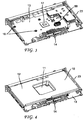
- the first embodiment can be appreciated by particular reference to Figs. 1- 4 .
- Fig. 1 shows an internal view of the set-top box 1 in an assembled form with a front portion of the set-top box removed according to the first embodiment.
- Fig. 1 shows a top broad heat sink 10, which is an internal component.
- the top broad heat sink 10 can be a generally contoured plate that has a generally planar periphery 12 and a contoured central feature such as a pocket, central depression, notch, recess, multilevel depression, or mesa extending from and/or into a plane of the planar periphery.
- the central feature or central depression 11 can have side walls extending from the planar periphery and form an obtuse angle therewith.
- the contoured feature can have a flat bottom designed to contact the main integrated circuit and/or other heat generating component 17 on a main printed circuit board 13 which can be below it.
- Fig. 1 further shows a main printed circuit board 13 or the like, which can be generally flat.
- the main printed circuit board 13 can have a main integrated circuit 17 or the like in a central region and holes for mounting and/or securing the main printed circuit board 13 to a frame pan 18.
- the main integrated circuit and other heat generating or hot components 17 can contact the flat bottom or other portion of the central depression 11 of the top broad heat sink 10, which can be in thermal contact with the other heat generating or hot components through a thermal joint 27 which could be a pad.
- the main printed circuit board 13 is shown being mounted and/or secured to embosses 20 of the frame pan 18 by use of screws, bolts or solder pad joints 43 through the holes or contact points in the circuit board 13, wherein the main printed circuit board 13 is effectively contacting the frame pan 18. This contact can be thermal contact.
- Fig. 2 shows a perspective view of the underside of the main printed main printed circuit board 13 or the like.
- the main printed circuit board 13 can have in a central region of holes and associated pins 16 for primary or additional mounting and/or securing the main printed circuit board 13 to a frame pan 18.
- Other features of the main printed circuit board are shown in the figure which can include jack panel connectors 15 at one edge and a button cluster 14 at another edge. These edges can be opposing edges.
- Fig. 2 shows how the smart card reader 61 can be positioned on the main printed circuit board 13.
- Fig. 3 shows another perspective view of the upper side of the main printed main printed circuit board 13 or the like in contact with the frame 18.
- Fig. 3 shows the main printed circuit board 13 can have main integrated circuit or other heat generating component 17 in a central region and holes and associated pins 16 for mounting and/or securing the main printed circuit board 13 to a frame pan 18. Additionally shown is the finned convecting heat sink 58.
- the finned convecting heat sink 58 is constructed of 24 fins in which there are four rows of flat evenly spaced fins with the planar portion oriented along the x-axis (or the long axis which is parallel to the front of the set-top box) and in which there are six columns of evenly spaced fins oriented along the y-axis (or short axis which is parallel to the sides of the set-top box).
- the finned convecting heat sink 58 having a long dimension in the x-axis being 17.78 mm, a short dimension in the y-axis being 10.18 mm, and a height being 10.11 mm. Keeping these dimensions within 20% of the stated dimensions can be effective.
- the gaps between the fins are U-shaped or V-shaped in which the depths of the gaps are greater than half the height of the finned convecting heat sink 58.
- Fig. 4 shows a perspective view of the top broad heat sink 10 on the main printed main printed circuit board 13.
- the top broad heat sink 10 substantially covers the main printed main printed circuit board 13.
- Fig. 1 further shows how the smart card reader 61 can be in contact with the main printed circuit board 13 and immediately thereunder.
- the smart card reader 61 is shown having a smart card 64 inserted therein through a smart card entrance port 63 in one of the outer sides 34.
- the smart card reader 61 is shown being in contact with at least one thermal pad joint 62 that conducts heat generated by the smart card reader 61 to the finned convecting heat sink 58 which is also in contact with the main printed circuit board 13 and positioned immediately thereon.
- heat via holes 65 are shown being in the a main printed circuit board 13 to permit the heat from the smart card reader 61 to propagate to the finned convecting heat sink 58.
- the heat via holes 65 can be copper plated and the population of the heat via holes can be located substantially along and over the perimeter of the smart card reader 61 and uniformly distributed over the smart card reader 61 to optimize heat transfer from the smart card reader 61. It is advantageous to have the total plan view area of the via holes exceeding one-half area the plan view area of the via hole region, which is the region where the finned convecting heat sink 58 or the second heat sink contacts circuit board or the thermal pad joint.
- the vias can have vertical walls and can have an aspect ratio, which is a width or diameter of the via hole to height ratio, of 0.5 to 10.
- the set-top box 1 in Fig. 1 can have an outer cover 28 that further includes an upper wall 31, lower wall 32, and multiple outer sides 34.
- the exterior side of the lower wall 32 can include rubber feet 33 which can be at least 6 mm in height to ensure adequate air entry under the set-top box for improved thermal management.
- Fig. 1 also shows at least one proximal vent 59 in one of the outer sides 34 which is positioned in the general proximity of the finned convecting heat sink 58. It is preferable that the proximal vent 59 be positioned in one of the vertical outer sides 34 at a place that is closest to the finned convecting heat sink 58. At least one general vent 60 is shown which can be at other locations on other outer sides 34. The general vents 60 can further assist with the dissipation of heat. Additionally, the frame pan 18 can have side walls 23 that have complementary vents 66 which can be aligned with the vents of the outer sides 34. Having the vents on the outer sides in the combination of top broad heat sink 10 and the finned convecting heat sink 58 eliminates or can eliminate the need for vents in the upper wall 31.
- Fig. 1 further shows outer gaps 41 between the side walls 23 of the frame pan 18 and the outer side 34 of the outer cover 28; inner gaps 40 between the edge of the planar periphery 12 of the top broad heat sink 12 and the side walls 23 of the frame pan 18; bottom gap 42 between the lower wall 32 of the outer cover 28 and the base 22 of the frame pan 18; and upper gap 44 between the upper wall 31 of the outer cover 28 and the planar periphery 12 of the top broad heat sink 10.
- the bottom gap 42 and upper gap 44 prevent the outer cover 28 from overheating.
- a patch or area of many copper-plated thru-hole vias is advantageously added in the board at the location of the smart card contacts.
- a thermally conductive pad is advantageously placed on the patch of vias 62 and a heat sink is advantageously placed on the pad.
- a top broad heat sink has proved to be an effective way to cool the main integrated circuit of the set-top box, but the smart card reader adds an additional thermal load that cannot be dissipated by the conventional top broad heat sink.
- the finned heat sink and proximal vents have enhanced the thermal management of the set-top box.
- the top broad radiating heat sink is advantageously split or divided into two parts or two separate heat sinks.
- One of the two parts is in thermal contact with the main integrated circuit in the set-top box.
- the other of the two parts is in thermal contact with the smart card through the patch or area of vias.
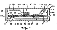
- Fig. 5 shows an internal view of the set-top box 1 in an assembled form with a front portion of the set-top box removed according to the second embodiment.
- Fig. 5 shows first top broad heat sink 10a, which is an internal component.
- the top broad heat sink 10a can be a generally contoured plate that has a generally planar periphery 12a and a contoured central feature such as a pocket, central depression, notch, recess, multilevel depression, or mesa extending from and/or into a plane of the planar periphery, wherein the planar periphery 12a preferably only surrounds part of the or central depression 11a.
- the planar periphery 12a surrounds 3 sides of the central depression 11a.
- the central feature or central depression 11a can have side walls extending from the planar periphery and form an obtuse angle therewith.
- the contoured feature can have a flat bottom designed to contact the main integrated circuit and/or other heat generating component 17 on a main printed circuit board 13 which can be below it.
- Fig. 5 also shows the second top broad heat sink 10b, which is an internal component.
- the top broad heat sink 10b can also be a generally contoured plate that has a generally planar periphery 12b and a contoured central feature such as a pocket, central depression, notch, recess, multilevel depression, mesa extending from and/or into a plane of the planar periphery, wherein the planar periphery 12b preferably only surrounds part of the central depression 11b.
- the planar periphery 12b surrounds 3 sides of the central depression 11b.
- the central feature or central depression 11b can have side walls extending from the planar periphery and form an obtuse angle therewith.
- the contoured feature can have a flat bottom designed to contact the main printed circuit board 13 in the region where the smart card reader 61 is located.
- the smart card reader 61 is shown being in contact with at least one thermal pad joint 62 that conducts heat generated by the smart card reader 61 to the second top broad heat sink 10b which is also in contact with the main printed circuit board 13 and thereon.
- heat transmissive via holes 65 are positioned in the main printed circuit board 13 to permit the heat from the smart card reader 61 to propagate to the second top broad heat sink 10b.
- the heat via holes 65 can be copper plated and the population of the heat via holes can be located substantially along the perimeter of the smart card reader 61 and uniformly distributed over the smart card reader 61 to optimize heat transfer from the smart card reader 61.
- the vias can have the same characteristics and dimensional aspects in this embodiment as in the first embodiment.
- the main printed circuit board 13, frame pan 18 and the outer cover 28 are generally the same as in the first embodiment of the invention.
- the frame pan 18 also can have complementary vents 66 which can be aligned with the vents 60 of the outer sides 34, wherein the edges of planar peripheries 12a, 12b run along the outer sides 34.
- the invention is applicable to computers and other electronic devices having heat generating components. Furthermore, the invention is also applicable to electronic parts other than circuit boards which can generate heat.
- the invention is not limited to the precise arrangements and instrumentalities shown. As such, the invention is intended to apply, for example, to heat source elements such as hard drives, smart card readers, integrated circuits, and light sources that could be used to light buttons. Further, when a heatsink is said to be contacting a heat source element, this can imply through direct contact or contact through an intermediary component such as via holes and/or thermal pads or thermal joints.
- vent can imply a single vent opening or multiple localized vent openings; the expression “substantially overlying” is intended to mean completely overlying or overlying at 90% of a surface of a structure; the expression “planar peripheral portion” can mean that the portion is completely planar or can include portions which are generally planar, but may have some raised portions or groves which may be needed to add structural integrity or may be needed to accommodate components in the set-top box.
Claims (14)
- Dispositif électronique (1) comprenant :un boîtier doté d'une première paroi extérieure verticale (34) avec une première aération (60) et d'une deuxième paroi extérieure verticale (34) avec une deuxième aération (59) ;une carte de circuit imprimé (13) ayant un premier élément de source de chaleur (17) et un deuxième élément de source de chaleur (61) ;un dissipateur thermique profilé (10, 10a) en contact thermique avec le premier élément de source de chaleur (17), dans lequel le dissipateur thermique profilé (10, 10a) recouvre au moins un tiers de la carte de circuit imprimé (13) et s'étend le long de la première paroi latérale verticale ;un deuxième dissipateur thermique (58, 10b) en contact avec le deuxième élément de source de chaleur (61), dans lequel le deuxième dissipateur thermique (58, 10b) se situe uniquement dans une moitié du dispositif électronique (1) et est aligné avec la deuxième aération (59) ;dans lequel le deuxième élément de source de chaleur (61) se situe sous la carte de circuit imprimé (13) et la carte de circuit imprimé (13) comporte des orifices de passage de la chaleur (65) sur le deuxième élément de source de chaleur (61), où la chaleur générée par le deuxième élément de source de chaleur (61) est transférée au deuxième dissipateur thermique (58, 10b) via les orifices de passage de la chaleur (65).
- Dispositif électronique selon la revendication 1, dans lequelle dissipateur thermique profilé (10, 10a) possède une partie périphérique planaire (12, 12a) et une partie en creux centrale (11, 11a),la partie périphérique planaire (12, 12a) entoure au moins une partie de la partie en creux centrale (11, 11a), etla partie en creux centrale (11, 11a) est en contact avec le premier élément de source de chaleur (17).
- Dispositif électronique selon la revendication 1 comprenant un cadre (18) doté d'une base (22) et de bossages (20), dans lequel la base (22) se situe sous la carte de circuit imprimé (13) et les bossages (20) sont en contact avec la carte de circuit imprimé (13) et la soutiennent.
- Dispositif électronique selon la revendication 3, dans lequelle cadre (18) possède au moins une première paroi latérale verticale (23) orientée le long de la première paroi extérieure verticale (34) et une deuxième paroi latérale verticale (23) orientée le long de la deuxième paroi extérieure verticale (34), etla première paroi latérale verticale (23) possède une première aération intérieure (66) alignée avec la première aération (60) et la deuxième paroi latérale verticale (23) possède une deuxième aération intérieure (66) alignée avec la deuxième aération (59).
- Dispositif électronique selon la revendication 2, dans lequelle dissipateur thermique profilé (10) possède une partie périphérique planaire (12) entourant complètement la partie en creux centrale (11), etle dissipateur thermique profilé (10) recouvre substantiellement la carte de circuit imprimé (13) et recouvre totalement le deuxième dissipateur thermique (58).
- Dispositif électronique selon la revendication 5, dans lequel le deuxième dissipateur thermique (58) est un dissipateur thermique à ailettes.
- Dispositif électronique selon la revendication 4 dans lequel le dissipateur thermique profilé (10) recouvre substantiellement la carte de circuit imprimé (13) et recouvre totalement le deuxième dissipateur thermique (58).
- Dispositif électronique selon la revendication 7, dans lequel le deuxième dissipateur thermique (58) est un dissipateur thermique à ailettes.
- Dispositif électronique selon la revendication 4, dans lequelle dissipateur thermique profilé (10) possède une partie périphérique planaire (12) entourant complètement une partie en creux centrale (11),le dissipateur thermique profilé (10) recouvre substantiellement la carte de circuit imprimé (13) et recouvre totalement le deuxième dissipateur thermique (58), etla partie en creux centrale (11) est en contact avec le premier élément de source de chaleur (17).
- Dispositif électronique selon la revendication 9, dans lequel le deuxième dissipateur thermique (58) est un dissipateur thermique à ailettes.
- Dispositif électronique selon la revendication 2, dans lequelle deuxième dissipateur thermique profilé (10b) possède une deuxième partie périphérique planaire (12b) et une deuxième partie en creux centrale (11b),la deuxième partie périphérique planaire (12b) entoure au moins une partie de la deuxième partie en creux centrale (11b), etla deuxième partie en creux centrale (11b) est en contact avec le deuxième élément de source de chaleur (61).
- Dispositif électronique selon la revendication 11, dans lequel le dissipateur thermique profilé (10a) recouvre moins de la moitié de la carte de circuit imprimé (13) et le deuxième dissipateur thermique (10b) recouvre plus d'un tiers de la carte de circuit imprimé (13).
- Dispositif électronique selon la revendication 12, comprenant un cadre (18) doté d'une base (22) et de bossages (20), dans lequella base (22) se situe sous la carte de circuit imprimé (13) et les bossages (20) sont en contact avec la carte de circuit imprimé (13) et la soutiennent,le cadre (18) possède au moins une première paroi latérale verticale (23) orientée le long de la première paroi extérieure verticale (34) et une deuxième paroi latérale verticale (23) orientée le long de la deuxième paroi extérieure verticale (34), etla première paroi latérale verticale (23) possède une première aération intérieure (66) alignée avec la première aération (60) et la deuxième paroi latérale verticale (23) possède une deuxième aération intérieure (66) alignée avec la deuxième aération (60).
- Dispositif électronique selon la revendication 13, dans lequel les orifices de passage de la chaleur (65) se situent sous la deuxième partie en creux centrale (11 b).
Applications Claiming Priority (3)
| Application Number | Priority Date | Filing Date | Title |
|---|---|---|---|
| US34607310P | 2010-05-19 | 2010-05-19 | |
| US40076710P | 2010-08-02 | 2010-08-02 | |
| PCT/US2011/036171 WO2011146302A1 (fr) | 2010-05-19 | 2011-05-12 | Boîtier décodeur permettant de dissiper les charges thermiques |
Publications (2)
| Publication Number | Publication Date |
|---|---|
| EP2572562A1 EP2572562A1 (fr) | 2013-03-27 |
| EP2572562B1 true EP2572562B1 (fr) | 2018-05-09 |
Family
ID=44484817
Family Applications (1)
| Application Number | Title | Priority Date | Filing Date |
|---|---|---|---|
| EP11724317.0A Not-in-force EP2572562B1 (fr) | 2010-05-19 | 2011-05-12 | Boîtier décodeur avec structure de dissipation de chaleur |
Country Status (7)
| Country | Link |
|---|---|
| US (1) | US9220185B2 (fr) |
| EP (1) | EP2572562B1 (fr) |
| JP (1) | JP2013527615A (fr) |
| KR (1) | KR20130077841A (fr) |
| CN (1) | CN103262675B (fr) |
| BR (1) | BR112012029464A2 (fr) |
| WO (1) | WO2011146302A1 (fr) |
Cited By (1)
| Publication number | Priority date | Publication date | Assignee | Title |
|---|---|---|---|---|
| CN106848539A (zh) * | 2017-01-19 | 2017-06-13 | 努比亚技术有限公司 | 一种天线装置 |
Families Citing this family (28)
| Publication number | Priority date | Publication date | Assignee | Title |
|---|---|---|---|---|
| KR20120129885A (ko) | 2009-12-09 | 2012-11-28 | 톰슨 라이센싱 | 마이크로천공을 구비하는 셋탑 박스 |
| KR20130029044A (ko) | 2010-02-25 | 2013-03-21 | 톰슨 라이센싱 | 퀵 릴리스 스냅들이 은닉된 소형 다층 방사성 냉각 케이스 |
| US9220185B2 (en) | 2010-05-19 | 2015-12-22 | Thomson Licensing | Set-top box having dissipating thermal loads |
| BR112013022150B1 (pt) | 2011-03-09 | 2022-06-21 | Interdigital Ce Patent Holdings | Dispositivo eletrônico |
| US8363411B2 (en) | 2011-03-18 | 2013-01-29 | Eldon Technology Limited | Passive, low-profile heat transferring system |
| US8619427B2 (en) | 2011-03-21 | 2013-12-31 | Eldon Technology Limited | Media content device chassis with internal extension members |
| US8681495B2 (en) * | 2011-03-29 | 2014-03-25 | Eldon Technology Limited | Media device having a piezoelectric fan |
| US9317079B2 (en) | 2011-03-29 | 2016-04-19 | Echostar Uk Holdings Limited | Media content device with customized panel |
| JP5792386B2 (ja) | 2011-07-14 | 2015-10-14 | トムソン ライセンシングThomson Licensing | スナップインヒートシンクとスマートカードリーダを有し、ヒートシンク保持用締め具を有するセットトップボックス |
| JP6130844B2 (ja) | 2011-10-19 | 2017-05-17 | トムソン ライセンシングThomson Licensing | ブラインドナビゲーションのためのフィードバックによるリモートコントロール |
| CN103547111B (zh) * | 2012-07-09 | 2016-08-10 | 光宝电子(广州)有限公司 | 平面式散热结构及电子装置 |
| EP3014963B1 (fr) | 2013-06-27 | 2019-08-07 | InterDigital CE Patent Holdings | Capot de dispositif pour gestion thermique |
| CN105683700A (zh) | 2013-08-16 | 2016-06-15 | 汤姆逊许可公司 | 具有隔离的对流翅片的多层散热器组件 |
| CN103491748B (zh) * | 2013-09-17 | 2016-06-08 | 深圳市九洲电器有限公司 | 散热装置和机顶盒 |
| WO2015061396A1 (fr) * | 2013-10-24 | 2015-04-30 | Technicolor Usa, Inc. | Montage d'antennes sans fil compactes à protection contre les décharges électrostatiques |
| US20160135282A1 (en) * | 2014-11-07 | 2016-05-12 | Kabushiki Kaisha Toshiba | Electronic apparatus |
| KR101491833B1 (ko) * | 2014-11-16 | 2015-02-11 | 가온미디어 주식회사 | 포집 분산형 히트싱크 |
| JP6601055B2 (ja) * | 2015-08-20 | 2019-11-06 | 富士通株式会社 | プリント配線板、電子機器及び実装方法 |
| US10356948B2 (en) | 2015-12-31 | 2019-07-16 | DISH Technologies L.L.C. | Self-adjustable heat spreader system for set-top box assemblies |
| KR101794007B1 (ko) | 2016-04-06 | 2017-11-07 | (주)휴맥스 | 방열모듈 조립체 및 이를 갖는 셋탑박스 |
| WO2019030809A1 (fr) * | 2017-08-08 | 2019-02-14 | Necプラットフォームズ株式会社 | Structure de rayonnement de chaleur |
| JP2019057656A (ja) * | 2017-09-22 | 2019-04-11 | ダイヤモンド電機株式会社 | 空冷機構付き電子機器 |
| US10721840B2 (en) | 2017-10-11 | 2020-07-21 | DISH Technologies L.L.C. | Heat spreader assembly |
| US11122707B2 (en) * | 2018-07-12 | 2021-09-14 | Arris Enterprises Llc | Raised pathway heat sink |
| KR20220041291A (ko) * | 2020-09-24 | 2022-04-01 | 삼성디스플레이 주식회사 | 표시 장치 및 이를 구비한 전자 기기 |
| US11647609B2 (en) * | 2020-12-15 | 2023-05-09 | Arris Enterprises Llc | Multisided heat spreader |
| US11800687B2 (en) * | 2021-08-26 | 2023-10-24 | Dish Network L.L.C. | Heat transfer assembly |
| US20230345675A1 (en) * | 2022-04-26 | 2023-10-26 | Dish Network, L.L.C. | Electronic assembly having thermal pad with polymer layer |
Family Cites Families (81)
| Publication number | Priority date | Publication date | Assignee | Title |
|---|---|---|---|---|
| US4887147A (en) | 1987-07-01 | 1989-12-12 | Digital Equipment Corporation | Thermal package for electronic components |
| JPH02307182A (ja) | 1989-05-23 | 1990-12-20 | Hitachi Maxell Ltd | Icカードリーダ・ライタ |
| JP2758283B2 (ja) | 1991-06-17 | 1998-05-28 | 株式会社東芝 | ハードディスクパックの脱着機構 |
| US6850252B1 (en) | 1999-10-05 | 2005-02-01 | Steven M. Hoffberg | Intelligent electronic appliance system and method |
| JPH06227553A (ja) | 1993-01-28 | 1994-08-16 | Yazaki Corp | ロック構造 |
| US5620242A (en) | 1993-04-19 | 1997-04-15 | Motorola, Inc. | Portable radio battery latch |
| JP3251734B2 (ja) | 1993-08-18 | 2002-01-28 | 株式会社日立テレコムテクノロジー | 電子装置の筐体構造 |
| JPH0786471A (ja) | 1993-09-20 | 1995-03-31 | Hitachi Ltd | 半導体モジュ−ル |
| US5667397A (en) | 1994-12-01 | 1997-09-16 | The Whitaker Corporation | Smart card connector |
| US5917236A (en) | 1995-12-08 | 1999-06-29 | Hewlett-Packard Company | Packaging system for field effects transistors |
| JP3776169B2 (ja) | 1996-06-13 | 2006-05-17 | 任天堂株式会社 | 電子機器の放熱構造 |
| JPH10154390A (ja) | 1996-11-20 | 1998-06-09 | Nippon Columbia Co Ltd | ディスク再生装置 |
| US6049469A (en) * | 1997-08-20 | 2000-04-11 | Dell Usa, L.P. | Combination electromagnetic shield and heat spreader |
| US7082033B1 (en) | 1998-02-13 | 2006-07-25 | Micron Technology, Inc. | Removing heat from integrated circuit devices mounted on a support structure |
| JP3597368B2 (ja) | 1998-02-16 | 2004-12-08 | アルプス電気株式会社 | 電子機器 |
| US6021044A (en) | 1998-08-13 | 2000-02-01 | Data General Corporation | Heatsink assembly |
| JP2000269671A (ja) | 1999-03-19 | 2000-09-29 | Toshiba Corp | 電子機器 |
| JP2000269675A (ja) | 1999-03-19 | 2000-09-29 | Sony Corp | 放熱装置およびセット・トップ・ボックス |
| US6411522B1 (en) | 1999-04-01 | 2002-06-25 | Western Digital Ventures, Inc. | Integrated computer module with EMI shielding plate |
| JP3982941B2 (ja) | 1999-04-12 | 2007-09-26 | 富士通株式会社 | 記憶装置 |
| US6382995B1 (en) | 1999-05-20 | 2002-05-07 | Itt Manufacturing Enterprises, Inc | Smart card connector with retain and eject means |
| DE69937103T2 (de) | 1999-06-08 | 2008-06-12 | Molex Inc., Lisle | Tragbare Chipkarten-Leseanordnung |
| KR20020027461A (ko) | 1999-07-02 | 2002-04-13 | 캐롤린 에이. 베이츠 | 스마트 카드 판독기 |
| JP2001147061A (ja) | 1999-09-08 | 2001-05-29 | Sega Corp | 冷却装置を有する電子機器 |
| GB2355017B (en) | 1999-09-23 | 2001-09-12 | Lorenzo Battisti | Porous element |
| US6212074B1 (en) | 2000-01-31 | 2001-04-03 | Sun Microsystems, Inc. | Apparatus for dissipating heat from a circuit board having a multilevel surface |
| JP3923703B2 (ja) | 2000-03-29 | 2007-06-06 | ローム株式会社 | 放熱手段を有するプリント配線板 |
| JP2001358482A (ja) | 2000-04-14 | 2001-12-26 | Matsushita Refrig Co Ltd | 放熱モジュール |
| FR2809871B1 (fr) | 2000-06-05 | 2002-07-19 | Itt Mfg Entpr S Inc | Connecteur electrique a lames de contact perfectionnees pour le raccordement d'une carte a circuit(s) integre(s) |
| US20020051338A1 (en) | 2000-07-27 | 2002-05-02 | Lixin Jiang | Acoustic enclosure for an air cooled hard disk drive |
| DE10051159C2 (de) | 2000-10-16 | 2002-09-19 | Osram Opto Semiconductors Gmbh | LED-Modul, z.B. Weißlichtquelle |
| JP2002134970A (ja) | 2000-10-26 | 2002-05-10 | Denso Corp | 電子制御装置 |
| US6524361B1 (en) | 2000-10-26 | 2003-02-25 | Hubbell Incorporated | Micro-porous filter |
| EP1248507A1 (fr) | 2001-04-04 | 2002-10-09 | Siemens Aktiengesellschaft | Module HF d' un appareil audio à dissipation thermique améliorée |
| JP2002324989A (ja) * | 2001-04-26 | 2002-11-08 | Murata Mach Ltd | 印刷回路基板の放熱構造 |
| JP4057796B2 (ja) | 2001-07-03 | 2008-03-05 | 株式会社東芝 | 非水電解質空気電池 |
| US6735085B2 (en) | 2002-08-15 | 2004-05-11 | Hon Hai Precision Ind. Co., Ltd. | Foldable retention device for land grid array connector assembly |
| JP2004186294A (ja) | 2002-12-02 | 2004-07-02 | Denso Corp | 電子装置 |
| JP4039316B2 (ja) * | 2003-06-09 | 2008-01-30 | 株式会社明電舎 | 電子機器の冷却構造 |
| ATE388487T1 (de) | 2003-08-07 | 2008-03-15 | Harman Becker Automotive Sys | Vorrichtung zur kühlung von halbleiterbauteilen auf leiterplatten |
| US7203065B1 (en) * | 2003-11-24 | 2007-04-10 | Ciena Corporation | Heatsink assembly |
| US20050128710A1 (en) * | 2003-12-15 | 2005-06-16 | Beiteimal Abdlmonem H. | Cooling system for electronic components |
| TWI256192B (en) | 2004-04-15 | 2006-06-01 | Acbel Polytech Inc | Power adapter with heat sink device |
| FR2871022B1 (fr) | 2004-05-25 | 2006-11-03 | Valeo Electronique Sys Liaison | Boitier pour circuits electriques ou electroniques |
| GB0413340D0 (en) | 2004-06-15 | 2004-07-21 | Pace Micro Tech Plc | Improvements to electrical apparatus |
| FR2875917B3 (fr) | 2004-09-29 | 2007-01-05 | Alvaro Lemos | Dispositif d'aeration pliable pour la protection de micro-ordinateurs portables |
| US7215551B2 (en) * | 2004-09-29 | 2007-05-08 | Super Talent Electronics, Inc. | Memory module assembly including heat sink attached to integrated circuits by adhesive |
| TWI247574B (en) | 2004-11-30 | 2006-01-11 | Silicon Integrated Sys Corp | Heat dissipation mechanism for electronic device |
| US7791874B2 (en) | 2004-12-30 | 2010-09-07 | Microsoft Corporation | Removable module for a console |
| JP2006229046A (ja) | 2005-02-18 | 2006-08-31 | Toshiba Corp | 電子機器の放熱装置及び放熱方法 |
| JP4445409B2 (ja) | 2005-02-23 | 2010-04-07 | 株式会社東芝 | 電子機器の放熱装置 |
| US7158380B2 (en) * | 2005-03-25 | 2007-01-02 | Scientific-Atlanta, Inc. | Heatsink for digital video recorder |
| US7350705B1 (en) | 2005-03-28 | 2008-04-01 | International Technologies & Systems Corp. | Compact robust smart card reader |
| DE202005013758U1 (de) | 2005-08-31 | 2006-01-19 | Sampo Corp., Kuei Shan Hsiang | Kühlmechanismus für ein tragbares digitales Fernsehgerät |
| US7272001B2 (en) | 2005-09-09 | 2007-09-18 | King Young Technology Co., Ltd. | External conductive heat dissipating device for microcomputers |
| WO2007089321A2 (fr) | 2005-11-23 | 2007-08-09 | Comcast Cable Holdings, Llc | Coffret d'abonné |
| US20070177356A1 (en) * | 2006-02-01 | 2007-08-02 | Jeffrey Panek | Three-dimensional cold plate and method of manufacturing same |
| JP4742893B2 (ja) | 2006-02-03 | 2011-08-10 | 日本電気株式会社 | 発熱デバイスの実装装置およびその放熱装置 |
| US7450387B2 (en) | 2006-03-02 | 2008-11-11 | Tdk Innoveta Technologies, Inc. | System for cooling electronic components |
| GB2436170A (en) | 2006-03-17 | 2007-09-19 | Amstrad Plc | Cooling or heating device in a chip card reader |
| US7664198B2 (en) | 2006-03-21 | 2010-02-16 | Kyocera Corporation | System and method for broadcasting data over a wireless network using rateless codes |
| JP2008034474A (ja) * | 2006-07-26 | 2008-02-14 | Sharp Corp | 伝熱シート及び基板装置 |
| US7518875B2 (en) | 2006-12-14 | 2009-04-14 | International Business Machines Corporation | Securing heat sinks to a device under test |
| CN101663673B (zh) | 2007-05-04 | 2016-09-07 | 汤姆逊许可证公司 | 智能卡散热装置 |
| DE202007006626U1 (de) | 2007-05-09 | 2007-10-04 | Hamburg Industries Co., Ltd., Shen Keng | Verbindungseinrichtung |
| US8023260B2 (en) | 2007-09-04 | 2011-09-20 | Apple Inc. | Assembly of an electronic device |
| WO2009057124A2 (fr) | 2007-11-01 | 2009-05-07 | Innomedia Technologies Pvt. Ltd. | Meuble pour boîtier décodeur pour le refroidissement naturel d'électronique interne |
| JP4857252B2 (ja) | 2007-12-07 | 2012-01-18 | 株式会社日立製作所 | 電子機器 |
| JP4473923B2 (ja) | 2008-10-22 | 2010-06-02 | 株式会社東芝 | 電子機器 |
| CN201352820Y (zh) | 2009-02-10 | 2009-11-25 | 深圳创维数字技术股份有限公司 | 机顶盒机箱 |
| FR2944408B1 (fr) | 2009-04-14 | 2012-09-21 | Eads Europ Aeronautic Defence | Boitier pour carte electronique embarquee |
| KR101552357B1 (ko) | 2009-05-29 | 2015-09-11 | 엘지이노텍 주식회사 | 튜너 모듈 |
| CN201515429U (zh) | 2009-09-22 | 2010-06-23 | 重庆迪特尔数字电视有限公司 | 数字电视机顶盒 |
| KR20120129885A (ko) | 2009-12-09 | 2012-11-28 | 톰슨 라이센싱 | 마이크로천공을 구비하는 셋탑 박스 |
| CN201571126U (zh) * | 2009-12-14 | 2010-09-01 | 福建创频数码科技有限公司 | 一种新型机顶盒外壳 |
| KR20130029044A (ko) | 2010-02-25 | 2013-03-21 | 톰슨 라이센싱 | 퀵 릴리스 스냅들이 은닉된 소형 다층 방사성 냉각 케이스 |
| US8620162B2 (en) | 2010-03-25 | 2013-12-31 | Apple Inc. | Handheld electronic device with integrated transmitters |
| US9220185B2 (en) | 2010-05-19 | 2015-12-22 | Thomson Licensing | Set-top box having dissipating thermal loads |
| USD631449S1 (en) | 2010-08-02 | 2011-01-25 | Thomson Licensing | Set top box |
| GB201016047D0 (en) | 2010-09-24 | 2010-11-10 | Pace Plc | Means for heating dissipation for electrical and/or electronic apparatus |
| BR112013022150B1 (pt) | 2011-03-09 | 2022-06-21 | Interdigital Ce Patent Holdings | Dispositivo eletrônico |
-
2011
- 2011-05-12 US US13/698,868 patent/US9220185B2/en not_active Expired - Fee Related
- 2011-05-12 BR BR112012029464A patent/BR112012029464A2/pt not_active Application Discontinuation
- 2011-05-12 EP EP11724317.0A patent/EP2572562B1/fr not_active Not-in-force
- 2011-05-12 WO PCT/US2011/036171 patent/WO2011146302A1/fr active Application Filing
- 2011-05-12 CN CN201180032238.7A patent/CN103262675B/zh not_active Expired - Fee Related
- 2011-05-12 KR KR1020127033169A patent/KR20130077841A/ko not_active Application Discontinuation
- 2011-05-12 JP JP2013511224A patent/JP2013527615A/ja active Pending
Non-Patent Citations (1)
| Title |
|---|
| None * |
Cited By (2)
| Publication number | Priority date | Publication date | Assignee | Title |
|---|---|---|---|---|
| CN106848539A (zh) * | 2017-01-19 | 2017-06-13 | 努比亚技术有限公司 | 一种天线装置 |
| CN106848539B (zh) * | 2017-01-19 | 2019-10-25 | 努比亚技术有限公司 | 一种天线装置 |
Also Published As
| Publication number | Publication date |
|---|---|
| KR20130077841A (ko) | 2013-07-09 |
| CN103262675A (zh) | 2013-08-21 |
| JP2013527615A (ja) | 2013-06-27 |
| EP2572562A1 (fr) | 2013-03-27 |
| US9220185B2 (en) | 2015-12-22 |
| US20130063895A1 (en) | 2013-03-14 |
| BR112012029464A2 (pt) | 2017-03-01 |
| CN103262675B (zh) | 2016-03-30 |
| WO2011146302A1 (fr) | 2011-11-24 |
Similar Documents
| Publication | Publication Date | Title |
|---|---|---|
| EP2572562B1 (fr) | Boîtier décodeur avec structure de dissipation de chaleur | |
| US7345885B2 (en) | Heat spreader with multiple stacked printed circuit boards | |
| US5390078A (en) | Apparatus for using an active circuit board as a heat sink | |
| US5557500A (en) | Heat dissipating arrangement in a portable computer | |
| US20110292624A1 (en) | Electronic control unit | |
| US10314204B2 (en) | Heatsink alignment to printed circuit board | |
| US7133288B2 (en) | Processor heat sink retention module and assembly | |
| US20180310395A1 (en) | MULTl-LAYER HEAT SPREADER ASSEMBLY WITH ISOLATED CONVECTIVE FINS | |
| US20140293545A1 (en) | Electronic device enclosures and heatsink structures with thermal management features | |
| US6982481B1 (en) | System for dissipating heat and shielding electromagnetic radiation produced by an electronic device | |
| US10141627B2 (en) | Compact wireless antennae mounting with electrostatic discharge protection | |
| US20090310302A1 (en) | Heat-dissipating structure having an external fan | |
| KR20060016236A (ko) | 데스크 탑 퍼스널 컴퓨터에 삽입되는 확장 기판 구조 | |
| US6961241B2 (en) | Electronic apparatus with natural convection structure | |
| EP1785807B1 (fr) | Refroidissement d'un petit appareil électronique avec un connecteur USB. | |
| US20090213549A1 (en) | Heat sink assembly | |
| US20240081014A1 (en) | Processor back-plate devices | |
| JP3224659U (ja) | 拡張カードコネクタ及び拡張カードモジュールアセンブリ | |
| JP3104491U (ja) | 放熱板を備えた配線基板および該配線基板を実装した電子機器 | |
| JPH11354695A (ja) | 放熱機構およびこの放熱機構を有する情報処理装置 | |
| JPH0727679Y2 (ja) | 印刷配線板装置 | |
| KR20030006472A (ko) | 반도체 패키지의 방열 장치 | |
| JP2001352189A (ja) | 電子回路パッケージの放熱構造 |
Legal Events
| Date | Code | Title | Description |
|---|---|---|---|
| PUAI | Public reference made under article 153(3) epc to a published international application that has entered the european phase |
Free format text: ORIGINAL CODE: 0009012 |
|
| 17P | Request for examination filed |
Effective date: 20121121 |
|
| AK | Designated contracting states |
Kind code of ref document: A1 Designated state(s): AL AT BE BG CH CY CZ DE DK EE ES FI FR GB GR HR HU IE IS IT LI LT LU LV MC MK MT NL NO PL PT RO RS SE SI SK SM TR |
|
| DAX | Request for extension of the european patent (deleted) | ||
| 17Q | First examination report despatched |
Effective date: 20160408 |
|
| GRAP | Despatch of communication of intention to grant a patent |
Free format text: ORIGINAL CODE: EPIDOSNIGR1 |
|
| GRAJ | Information related to disapproval of communication of intention to grant by the applicant or resumption of examination proceedings by the epo deleted |
Free format text: ORIGINAL CODE: EPIDOSDIGR1 |
|
| INTG | Intention to grant announced |
Effective date: 20170816 |
|
| RIN1 | Information on inventor provided before grant (corrected) |
Inventor name: RITTER, DARIN, BRADLEY Inventor name: DIEMER, RODGER, ANTHONY Inventor name: GYSIN, MARK, WILLIAM Inventor name: HUNT, MICKEY, JAY |
|
| INTG | Intention to grant announced |
Effective date: 20170830 |
|
| INTC | Intention to grant announced (deleted) | ||
| GRAP | Despatch of communication of intention to grant a patent |
Free format text: ORIGINAL CODE: EPIDOSNIGR1 |
|
| INTG | Intention to grant announced |
Effective date: 20171114 |
|
| GRAS | Grant fee paid |
Free format text: ORIGINAL CODE: EPIDOSNIGR3 |
|
| GRAJ | Information related to disapproval of communication of intention to grant by the applicant or resumption of examination proceedings by the epo deleted |
Free format text: ORIGINAL CODE: EPIDOSDIGR1 |
|
| GRAL | Information related to payment of fee for publishing/printing deleted |
Free format text: ORIGINAL CODE: EPIDOSDIGR3 |
|
| GRAR | Information related to intention to grant a patent recorded |
Free format text: ORIGINAL CODE: EPIDOSNIGR71 |
|
| GRAA | (expected) grant |
Free format text: ORIGINAL CODE: 0009210 |
|
| INTC | Intention to grant announced (deleted) | ||
| INTG | Intention to grant announced |
Effective date: 20180326 |
|
| AK | Designated contracting states |
Kind code of ref document: B1 Designated state(s): AL AT BE BG CH CY CZ DE DK EE ES FI FR GB GR HR HU IE IS IT LI LT LU LV MC MK MT NL NO PL PT RO RS SE SI SK SM TR |
|
| REG | Reference to a national code |
Ref country code: GB Ref legal event code: FG4D |
|
| REG | Reference to a national code |
Ref country code: CH Ref legal event code: EP Ref country code: AT Ref legal event code: REF Ref document number: 998681 Country of ref document: AT Kind code of ref document: T Effective date: 20180515 |
|
| REG | Reference to a national code |
Ref country code: IE Ref legal event code: FG4D |
|
| REG | Reference to a national code |
Ref country code: DE Ref legal event code: R096 Ref document number: 602011048215 Country of ref document: DE |
|
| REG | Reference to a national code |
Ref country code: DE Ref legal event code: R084 Ref document number: 602011048215 Country of ref document: DE |
|
| REG | Reference to a national code |
Ref country code: NL Ref legal event code: MP Effective date: 20180509 |
|
| REG | Reference to a national code |
Ref country code: LT Ref legal event code: MG4D |
|
| PG25 | Lapsed in a contracting state [announced via postgrant information from national office to epo] |
Ref country code: ES Free format text: LAPSE BECAUSE OF FAILURE TO SUBMIT A TRANSLATION OF THE DESCRIPTION OR TO PAY THE FEE WITHIN THE PRESCRIBED TIME-LIMIT Effective date: 20180509 Ref country code: SE Free format text: LAPSE BECAUSE OF FAILURE TO SUBMIT A TRANSLATION OF THE DESCRIPTION OR TO PAY THE FEE WITHIN THE PRESCRIBED TIME-LIMIT Effective date: 20180509 Ref country code: BG Free format text: LAPSE BECAUSE OF FAILURE TO SUBMIT A TRANSLATION OF THE DESCRIPTION OR TO PAY THE FEE WITHIN THE PRESCRIBED TIME-LIMIT Effective date: 20180809 Ref country code: NO Free format text: LAPSE BECAUSE OF FAILURE TO SUBMIT A TRANSLATION OF THE DESCRIPTION OR TO PAY THE FEE WITHIN THE PRESCRIBED TIME-LIMIT Effective date: 20180809 Ref country code: FI Free format text: LAPSE BECAUSE OF FAILURE TO SUBMIT A TRANSLATION OF THE DESCRIPTION OR TO PAY THE FEE WITHIN THE PRESCRIBED TIME-LIMIT Effective date: 20180509 Ref country code: LT Free format text: LAPSE BECAUSE OF FAILURE TO SUBMIT A TRANSLATION OF THE DESCRIPTION OR TO PAY THE FEE WITHIN THE PRESCRIBED TIME-LIMIT Effective date: 20180509 |
|
| PG25 | Lapsed in a contracting state [announced via postgrant information from national office to epo] |
Ref country code: HR Free format text: LAPSE BECAUSE OF FAILURE TO SUBMIT A TRANSLATION OF THE DESCRIPTION OR TO PAY THE FEE WITHIN THE PRESCRIBED TIME-LIMIT Effective date: 20180509 Ref country code: LV Free format text: LAPSE BECAUSE OF FAILURE TO SUBMIT A TRANSLATION OF THE DESCRIPTION OR TO PAY THE FEE WITHIN THE PRESCRIBED TIME-LIMIT Effective date: 20180509 Ref country code: NL Free format text: LAPSE BECAUSE OF FAILURE TO SUBMIT A TRANSLATION OF THE DESCRIPTION OR TO PAY THE FEE WITHIN THE PRESCRIBED TIME-LIMIT Effective date: 20180509 Ref country code: RS Free format text: LAPSE BECAUSE OF FAILURE TO SUBMIT A TRANSLATION OF THE DESCRIPTION OR TO PAY THE FEE WITHIN THE PRESCRIBED TIME-LIMIT Effective date: 20180509 Ref country code: GR Free format text: LAPSE BECAUSE OF FAILURE TO SUBMIT A TRANSLATION OF THE DESCRIPTION OR TO PAY THE FEE WITHIN THE PRESCRIBED TIME-LIMIT Effective date: 20180810 |
|
| REG | Reference to a national code |
Ref country code: DE Ref legal event code: R119 Ref document number: 602011048215 Country of ref document: DE |
|
| REG | Reference to a national code |
Ref country code: CH Ref legal event code: PL |
|
| REG | Reference to a national code |
Ref country code: AT Ref legal event code: MK05 Ref document number: 998681 Country of ref document: AT Kind code of ref document: T Effective date: 20180509 |
|
| REG | Reference to a national code |
Ref country code: BE Ref legal event code: MM Effective date: 20180531 |
|
| PG25 | Lapsed in a contracting state [announced via postgrant information from national office to epo] |
Ref country code: RO Free format text: LAPSE BECAUSE OF FAILURE TO SUBMIT A TRANSLATION OF THE DESCRIPTION OR TO PAY THE FEE WITHIN THE PRESCRIBED TIME-LIMIT Effective date: 20180509 Ref country code: CZ Free format text: LAPSE BECAUSE OF FAILURE TO SUBMIT A TRANSLATION OF THE DESCRIPTION OR TO PAY THE FEE WITHIN THE PRESCRIBED TIME-LIMIT Effective date: 20180509 Ref country code: DK Free format text: LAPSE BECAUSE OF FAILURE TO SUBMIT A TRANSLATION OF THE DESCRIPTION OR TO PAY THE FEE WITHIN THE PRESCRIBED TIME-LIMIT Effective date: 20180509 Ref country code: EE Free format text: LAPSE BECAUSE OF FAILURE TO SUBMIT A TRANSLATION OF THE DESCRIPTION OR TO PAY THE FEE WITHIN THE PRESCRIBED TIME-LIMIT Effective date: 20180509 Ref country code: PL Free format text: LAPSE BECAUSE OF FAILURE TO SUBMIT A TRANSLATION OF THE DESCRIPTION OR TO PAY THE FEE WITHIN THE PRESCRIBED TIME-LIMIT Effective date: 20180509 Ref country code: AT Free format text: LAPSE BECAUSE OF FAILURE TO SUBMIT A TRANSLATION OF THE DESCRIPTION OR TO PAY THE FEE WITHIN THE PRESCRIBED TIME-LIMIT Effective date: 20180509 Ref country code: SK Free format text: LAPSE BECAUSE OF FAILURE TO SUBMIT A TRANSLATION OF THE DESCRIPTION OR TO PAY THE FEE WITHIN THE PRESCRIBED TIME-LIMIT Effective date: 20180509 |
|
| REG | Reference to a national code |
Ref country code: IE Ref legal event code: MM4A |
|
| PG25 | Lapsed in a contracting state [announced via postgrant information from national office to epo] |
Ref country code: IT Free format text: LAPSE BECAUSE OF FAILURE TO SUBMIT A TRANSLATION OF THE DESCRIPTION OR TO PAY THE FEE WITHIN THE PRESCRIBED TIME-LIMIT Effective date: 20180509 Ref country code: LI Free format text: LAPSE BECAUSE OF NON-PAYMENT OF DUE FEES Effective date: 20180531 Ref country code: SM Free format text: LAPSE BECAUSE OF FAILURE TO SUBMIT A TRANSLATION OF THE DESCRIPTION OR TO PAY THE FEE WITHIN THE PRESCRIBED TIME-LIMIT Effective date: 20180509 Ref country code: CH Free format text: LAPSE BECAUSE OF NON-PAYMENT OF DUE FEES Effective date: 20180531 |
|
| PLBE | No opposition filed within time limit |
Free format text: ORIGINAL CODE: 0009261 |
|
| STAA | Information on the status of an ep patent application or granted ep patent |
Free format text: STATUS: NO OPPOSITION FILED WITHIN TIME LIMIT |
|
| PG25 | Lapsed in a contracting state [announced via postgrant information from national office to epo] |
Ref country code: MC Free format text: LAPSE BECAUSE OF FAILURE TO SUBMIT A TRANSLATION OF THE DESCRIPTION OR TO PAY THE FEE WITHIN THE PRESCRIBED TIME-LIMIT Effective date: 20180509 Ref country code: LU Free format text: LAPSE BECAUSE OF NON-PAYMENT OF DUE FEES Effective date: 20180512 |
|
| 26N | No opposition filed |
Effective date: 20190212 |
|
| GBPC | Gb: european patent ceased through non-payment of renewal fee |
Effective date: 20180809 |
|
| PG25 | Lapsed in a contracting state [announced via postgrant information from national office to epo] |
Ref country code: DE Free format text: LAPSE BECAUSE OF NON-PAYMENT OF DUE FEES Effective date: 20181201 Ref country code: FR Free format text: LAPSE BECAUSE OF NON-PAYMENT OF DUE FEES Effective date: 20180709 Ref country code: IE Free format text: LAPSE BECAUSE OF NON-PAYMENT OF DUE FEES Effective date: 20180512 |
|
| PG25 | Lapsed in a contracting state [announced via postgrant information from national office to epo] |
Ref country code: SI Free format text: LAPSE BECAUSE OF FAILURE TO SUBMIT A TRANSLATION OF THE DESCRIPTION OR TO PAY THE FEE WITHIN THE PRESCRIBED TIME-LIMIT Effective date: 20180509 Ref country code: BE Free format text: LAPSE BECAUSE OF NON-PAYMENT OF DUE FEES Effective date: 20180531 |
|
| PG25 | Lapsed in a contracting state [announced via postgrant information from national office to epo] |
Ref country code: GB Free format text: LAPSE BECAUSE OF NON-PAYMENT OF DUE FEES Effective date: 20180809 |
|
| PG25 | Lapsed in a contracting state [announced via postgrant information from national office to epo] |
Ref country code: AL Free format text: LAPSE BECAUSE OF FAILURE TO SUBMIT A TRANSLATION OF THE DESCRIPTION OR TO PAY THE FEE WITHIN THE PRESCRIBED TIME-LIMIT Effective date: 20180509 |
|
| PG25 | Lapsed in a contracting state [announced via postgrant information from national office to epo] |
Ref country code: MT Free format text: LAPSE BECAUSE OF NON-PAYMENT OF DUE FEES Effective date: 20180512 |
|
| PG25 | Lapsed in a contracting state [announced via postgrant information from national office to epo] |
Ref country code: TR Free format text: LAPSE BECAUSE OF FAILURE TO SUBMIT A TRANSLATION OF THE DESCRIPTION OR TO PAY THE FEE WITHIN THE PRESCRIBED TIME-LIMIT Effective date: 20180509 |
|
| PG25 | Lapsed in a contracting state [announced via postgrant information from national office to epo] |
Ref country code: HU Free format text: LAPSE BECAUSE OF FAILURE TO SUBMIT A TRANSLATION OF THE DESCRIPTION OR TO PAY THE FEE WITHIN THE PRESCRIBED TIME-LIMIT; INVALID AB INITIO Effective date: 20110512 Ref country code: PT Free format text: LAPSE BECAUSE OF FAILURE TO SUBMIT A TRANSLATION OF THE DESCRIPTION OR TO PAY THE FEE WITHIN THE PRESCRIBED TIME-LIMIT Effective date: 20180509 |
|
| PG25 | Lapsed in a contracting state [announced via postgrant information from national office to epo] |
Ref country code: CY Free format text: LAPSE BECAUSE OF FAILURE TO SUBMIT A TRANSLATION OF THE DESCRIPTION OR TO PAY THE FEE WITHIN THE PRESCRIBED TIME-LIMIT Effective date: 20180509 Ref country code: MK Free format text: LAPSE BECAUSE OF NON-PAYMENT OF DUE FEES Effective date: 20180509 |
|
| PG25 | Lapsed in a contracting state [announced via postgrant information from national office to epo] |
Ref country code: IS Free format text: LAPSE BECAUSE OF FAILURE TO SUBMIT A TRANSLATION OF THE DESCRIPTION OR TO PAY THE FEE WITHIN THE PRESCRIBED TIME-LIMIT Effective date: 20180909 |