EP2525408A1 - Oxidhalbleitervorrichtungen, Verfahren zur Herstellung der Oxidhalbleitervorrichtungen, Anzeigevorrichtungen mit den Oxidhalbleitervorrichtungen, Verfahren zur Herstellung der Anzeigevorrichtungen mit den Oxidhalbleitervorrichtungen - Google Patents
Oxidhalbleitervorrichtungen, Verfahren zur Herstellung der Oxidhalbleitervorrichtungen, Anzeigevorrichtungen mit den Oxidhalbleitervorrichtungen, Verfahren zur Herstellung der Anzeigevorrichtungen mit den Oxidhalbleitervorrichtungen Download PDFInfo
- Publication number
- EP2525408A1 EP2525408A1 EP11190716A EP11190716A EP2525408A1 EP 2525408 A1 EP2525408 A1 EP 2525408A1 EP 11190716 A EP11190716 A EP 11190716A EP 11190716 A EP11190716 A EP 11190716A EP 2525408 A1 EP2525408 A1 EP 2525408A1
- Authority
- EP
- European Patent Office
- Prior art keywords
- electrode
- insulation layer
- gate insulation
- oxide semiconductor
- layer
- Prior art date
- Legal status (The legal status is an assumption and is not a legal conclusion. Google has not performed a legal analysis and makes no representation as to the accuracy of the status listed.)
- Granted
Links
Images


Classifications
-
- H—ELECTRICITY
- H10—SEMICONDUCTOR DEVICES; ELECTRIC SOLID-STATE DEVICES NOT OTHERWISE PROVIDED FOR
- H10D—INORGANIC ELECTRIC SEMICONDUCTOR DEVICES
- H10D30/00—Field-effect transistors [FET]
- H10D30/60—Insulated-gate field-effect transistors [IGFET]
- H10D30/67—Thin-film transistors [TFT]
- H10D30/6729—Thin-film transistors [TFT] characterised by the electrodes
- H10D30/673—Thin-film transistors [TFT] characterised by the electrodes characterised by the shapes, relative sizes or dispositions of the gate electrodes
-
- H—ELECTRICITY
- H10—SEMICONDUCTOR DEVICES; ELECTRIC SOLID-STATE DEVICES NOT OTHERWISE PROVIDED FOR
- H10D—INORGANIC ELECTRIC SEMICONDUCTOR DEVICES
- H10D86/00—Integrated devices formed in or on insulating or conducting substrates, e.g. formed in silicon-on-insulator [SOI] substrates or on stainless steel or glass substrates
- H10D86/01—Manufacture or treatment
- H10D86/021—Manufacture or treatment of multiple TFTs
-
- H—ELECTRICITY
- H10—SEMICONDUCTOR DEVICES; ELECTRIC SOLID-STATE DEVICES NOT OTHERWISE PROVIDED FOR
- H10D—INORGANIC ELECTRIC SEMICONDUCTOR DEVICES
- H10D30/00—Field-effect transistors [FET]
- H10D30/01—Manufacture or treatment
- H10D30/021—Manufacture or treatment of FETs having insulated gates [IGFET]
- H10D30/031—Manufacture or treatment of FETs having insulated gates [IGFET] of thin-film transistors [TFT]
-
- H—ELECTRICITY
- H10—SEMICONDUCTOR DEVICES; ELECTRIC SOLID-STATE DEVICES NOT OTHERWISE PROVIDED FOR
- H10D—INORGANIC ELECTRIC SEMICONDUCTOR DEVICES
- H10D30/00—Field-effect transistors [FET]
- H10D30/60—Insulated-gate field-effect transistors [IGFET]
- H10D30/67—Thin-film transistors [TFT]
- H10D30/6704—Thin-film transistors [TFT] having supplementary regions or layers in the thin films or in the insulated bulk substrates for controlling properties of the device
- H10D30/6713—Thin-film transistors [TFT] having supplementary regions or layers in the thin films or in the insulated bulk substrates for controlling properties of the device characterised by the properties of the source or drain regions, e.g. compositions or sectional shapes
-
- H—ELECTRICITY
- H10—SEMICONDUCTOR DEVICES; ELECTRIC SOLID-STATE DEVICES NOT OTHERWISE PROVIDED FOR
- H10D—INORGANIC ELECTRIC SEMICONDUCTOR DEVICES
- H10D30/00—Field-effect transistors [FET]
- H10D30/60—Insulated-gate field-effect transistors [IGFET]
- H10D30/67—Thin-film transistors [TFT]
- H10D30/6729—Thin-film transistors [TFT] characterised by the electrodes
- H10D30/6737—Thin-film transistors [TFT] characterised by the electrodes characterised by the electrode materials
- H10D30/6739—Conductor-insulator-semiconductor electrodes
-
- H—ELECTRICITY
- H10—SEMICONDUCTOR DEVICES; ELECTRIC SOLID-STATE DEVICES NOT OTHERWISE PROVIDED FOR
- H10D—INORGANIC ELECTRIC SEMICONDUCTOR DEVICES
- H10D30/00—Field-effect transistors [FET]
- H10D30/60—Insulated-gate field-effect transistors [IGFET]
- H10D30/67—Thin-film transistors [TFT]
- H10D30/674—Thin-film transistors [TFT] characterised by the active materials
- H10D30/6755—Oxide semiconductors, e.g. zinc oxide, copper aluminium oxide or cadmium stannate
-
- H—ELECTRICITY
- H10—SEMICONDUCTOR DEVICES; ELECTRIC SOLID-STATE DEVICES NOT OTHERWISE PROVIDED FOR
- H10D—INORGANIC ELECTRIC SEMICONDUCTOR DEVICES
- H10D30/00—Field-effect transistors [FET]
- H10D30/60—Insulated-gate field-effect transistors [IGFET]
- H10D30/67—Thin-film transistors [TFT]
- H10D30/6757—Thin-film transistors [TFT] characterised by the structure of the channel, e.g. transverse or longitudinal shape or doping profile
-
- H10D64/011—
-
- H—ELECTRICITY
- H10—SEMICONDUCTOR DEVICES; ELECTRIC SOLID-STATE DEVICES NOT OTHERWISE PROVIDED FOR
- H10D—INORGANIC ELECTRIC SEMICONDUCTOR DEVICES
- H10D86/00—Integrated devices formed in or on insulating or conducting substrates, e.g. formed in silicon-on-insulator [SOI] substrates or on stainless steel or glass substrates
- H10D86/40—Integrated devices formed in or on insulating or conducting substrates, e.g. formed in silicon-on-insulator [SOI] substrates or on stainless steel or glass substrates characterised by multiple TFTs
- H10D86/421—Integrated devices formed in or on insulating or conducting substrates, e.g. formed in silicon-on-insulator [SOI] substrates or on stainless steel or glass substrates characterised by multiple TFTs having a particular composition, shape or crystalline structure of the active layer
- H10D86/423—Integrated devices formed in or on insulating or conducting substrates, e.g. formed in silicon-on-insulator [SOI] substrates or on stainless steel or glass substrates characterised by multiple TFTs having a particular composition, shape or crystalline structure of the active layer comprising semiconductor materials not belonging to the Group IV, e.g. InGaZnO
-
- H—ELECTRICITY
- H10—SEMICONDUCTOR DEVICES; ELECTRIC SOLID-STATE DEVICES NOT OTHERWISE PROVIDED FOR
- H10D—INORGANIC ELECTRIC SEMICONDUCTOR DEVICES
- H10D86/00—Integrated devices formed in or on insulating or conducting substrates, e.g. formed in silicon-on-insulator [SOI] substrates or on stainless steel or glass substrates
- H10D86/40—Integrated devices formed in or on insulating or conducting substrates, e.g. formed in silicon-on-insulator [SOI] substrates or on stainless steel or glass substrates characterised by multiple TFTs
- H10D86/60—Integrated devices formed in or on insulating or conducting substrates, e.g. formed in silicon-on-insulator [SOI] substrates or on stainless steel or glass substrates characterised by multiple TFTs wherein the TFTs are in active matrices
-
- H—ELECTRICITY
- H10—SEMICONDUCTOR DEVICES; ELECTRIC SOLID-STATE DEVICES NOT OTHERWISE PROVIDED FOR
- H10D—INORGANIC ELECTRIC SEMICONDUCTOR DEVICES
- H10D99/00—Subject matter not provided for in other groups of this subclass
-
- H10P50/267—
-
- H10P50/69—
-
- H10P70/23—
-
- H10P95/90—
-
- H—ELECTRICITY
- H10—SEMICONDUCTOR DEVICES; ELECTRIC SOLID-STATE DEVICES NOT OTHERWISE PROVIDED FOR
- H10K—ORGANIC ELECTRIC SOLID-STATE DEVICES
- H10K59/00—Integrated devices, or assemblies of multiple devices, comprising at least one organic light-emitting element covered by group H10K50/00
- H10K59/10—OLED displays
- H10K59/12—Active-matrix OLED [AMOLED] displays
- H10K59/1201—Manufacture or treatment
Definitions
- a preliminary recess structure may be formed on the gate insulation layer by performing a plasma treatment on the gate insulation layer between the source electrode and the drain electrode.
- the recess structure may be formed on the gate insulation layer by a cleaning treatment performed on the gate insulation layer having the preliminary recess structure.
- the mask pattern may be removed from the source electrode and the drain electrode.
- a first electrode film may be formed on the gate insulation layer, and a second electrode film may be formed on the first electrode film.
- the second electrode film may be obtained by nitriding the first electrode film.
- the second electrode film may be formed by thermally treating the first electrode film under an atmosphere containing nitrogen and/or by treating the first electrode film with a plasma generated from a gas containing nitrogen.
- the second electrode film and the first electrode film may be partially etched to form a first electrode pattern and a second electrode pattern on a first portion of the gate insulation layer, and to form a third electrode pattern and a fourth electrode pattern on a second portion of the gate insulation layer.
- the mask pattern from may be removed the source electrode and the drain electrode.
- a plasma treatment and/or a cleaning treatment may be performed on the gate insulation layer between the source electrode and the drain electrode.
- a display device including a substrate, a gate electrode on the substrate, a gate insulation layer on the substrate, a source electrode on a first portion of the gate insulation layer, a drain electrode on a second portion of the gate insulation layer, an active pattern on the source electrode and the drain electrode, a first electrode electrically connected to the drain electrode, a light emitting layer on the first electrode, and a second electrode on the light emitting layer.
- the gate insulation layer may include a recess structure over the gate electrode, and the active pattern may fill the recess structure;
- the recess structure may have a sidewall having a first angle of inclination relative to the substrate, and each of the source electrode and the drain electrode may have a sidewall having a second angle of inclination with respect to the substrate.
- the second angle of inclination may be substantially greater than the first angle of inclination.
- the gate insulation layer may have a substantially level upper face, and a ratio between a depth of the recess structure and a thickness of the gate insulation layer may be in a range from about 1.0:1.7 to about 1.0:30.0.
- a gate electrode may be formed on a substrate.
- a gate insulation layer may be formed on the substrate to cover the gate electrode.
- An electrode layer may be formed on the gate insulation layer.
- a mask pattern may be formed on the electrode layer.
- a source electrode and a drain electrode may be formed on the gate insulation layer by etching the electrode layer using the mask pattern.
- a recess structure may be formed on the gate insulation layer and between the source electrode and the drain electrode.
- An active pattern may be formed on the gate insulation layer, the source electrode and the drain electrode.
- a first electrode may be formed to be electrically connected to the drain electrode.
- a light emitting layer may be formed on the first electrode.
- a second electrode may be formed on the light emitting layer.
- the recess structure may be obtained by performing a plasma treatment and/or a cleaning treatment.
- a preliminary recess structure may be formed on the gate insulation layer by performing a plasma treatment on the gate insulation layer between the source electrode and the drain electrode.
- the mask pattern may be removed from the source electrode and the drain electrode.
- a cleaning treatment may be performed on the gate insulation layer having the preliminary recess structure.
- a first electrode film may be formed on the gate insulation layer, and a second electrode film may be formed on the first electrode film by nitriding the first electrode film.
- the second electrode film and the first electrode film may be partially etched to form a first electrode pattern and a second electrode pattern on a first portion of the gate insulation layer, and to form a third electrode pattern and a fourth electrode pattern on a second portion of the gate insulation layer.
- the mask pattern may be removed from the source electrode and the drain electrode, and then a plasma treatment and/or a cleaning treatment may be performed on the gate insulation layer between the source electrode and the drain electrode.
- the charge mobility and the operation current of the oxide semiconductor device may be further enhanced because the gate insulation layer may have a small thickness reduced by the recess structure.
- the oxide semiconductor device is employed in a display device such as an organic light emitting display device, a liquid crystal display device or a flexible display device, the display device may have various advantages, for example, a reduced thickness, an increased operation speed, an enhanced quality of displayed images, etc.
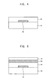
- FIG. 3 is a flow chart illustrating a method of manufacturing an oxide semiconductor device in accordance with some example embodiments of the present invention.
- FIG. 9 is a flow chart illustrating a method of manufacturing an oxide semiconductor device in accordance with some example embodiments of the present invention.
- FIGS. 10, 11 , and 12 are cross-sectional views illustrating a method of manufacturing an oxide semiconductor device in accordance with some example embodiments of the present invention.
- FIG. 13 is a flow chart illustrating a method of manufacturing an oxide semiconductor device in accordance with some example embodiments of the present invention.
- FIG. 16 is a flow chart illustrating a method of manufacturing an oxide semiconductor device in accordance with some example embodiments of the present invention.
- FIGS. 17, 18 , 19, and 20 are cross-sectional views illustrating a method of manufacturing an oxide semiconductor device in accordance with some example embodiments of the present invention.
- FIGS. 22 and 23 are cross-sectional views illustrating a method of manufacturing an oxide semiconductor device in accordance with some example embodiments of the present invention.
- FIG. 24 is a cross-sectional view illustrating a display device including an oxide semiconductor device in accordance with example embodiments of the present invention.
- first, second, third, etc. may be used herein to describe various elements, components, regions, layers and/or sections, these elements, components, regions, layers and/or sections should not be limited by these terms. These terms are only used to distinguish one element, component, region, layer or section from another region, layer or section. Thus, a first element, component, region, layer or section discussed below could be termed a second element, component, region, layer or section without departing from the teachings of example embodiments.
- spatially relative terms such as “beneath,” “below,” “lower,” “above,” “upper” and the like, may be used herein for ease of description to describe one element or feature's relationship to another element(s) or feature(s) as illustrated in the figures. It will be understood that the spatially relative terms are intended to encompass different orientations of the device in use or operation in addition to the orientation depicted in the figures. For example, if the device in the figures is turned over, elements described as “below” or “beneath” other elements or features would then be oriented “above” the other elements or features. Thus, the exemplary term “below” can encompass both an orientation of above and below. The device may be otherwise oriented (rotated 90 degrees or at other orientations) and the spatially relative descriptors used herein interpreted accordingly.
- Example embodiments are described herein with reference to cross-sectional illustrations that are schematic illustrations of idealized example embodiments (and intermediate structures). As such, variations from the shapes of the illustrations as a result, for example, of manufacturing techniques and/or tolerances, are to be expected. Thus, example embodiments should not be construed as limited to the particular shapes of regions illustrated herein but are to include deviations in shapes that result, for example, from manufacturing. For example, an implanted region illustrated as a rectangle will, typically, have rounded or curved features and/or a gradient of implant concentration at its edges rather than a binary change from implanted to non-implanted region.
- a buried region formed by implantation may result in some implantation in the region between the buried region and the surface through which the implantation takes place.
- the regions illustrated in the figures are schematic in nature and their shapes are not intended to illustrate the actual shape of a region of a device and are not intended to limit the scope of example embodiments.
- the oxide semiconductor device is provided on a substrate 5.
- the oxide semiconductor device includes a gate electrode 10, a gate insulation layer 15, a source electrode 20, a drain electrode 25 and an active pattern 30.
- the substrate 5 may include a transparent insulation substrate.
- the substrate 5 may include a glass substrate, a quartz substrate, a transparent plastic glass, a transparent metal oxide substrate, etc.
- a buffer layer is disposed on the substrate 5.
- the buffer layer may prevent the diffusion of impurities from the substrate 5 and may improve the flatness (e.g., an entire flatness) of the substrate 5.
- an upper face of the substrate 5 may be relatively uneven, the buffer layer having a substantially level (e.g., even or flat) upper face may be disposed on the substrate 5.
- a stress generated in a formation of the gate electrode 10 may be reduced, so that the gate electrode 10 may be easily provided on the substrate 5.
- the buffer layer may include a silicon compound.
- the buffer layer may include silicon oxide (SiOx), silicon nitride (SiNx), silicon oxynitride (SiOxNy), etc.
- the buffer layer may have a single layer structure having one silicon compound film, or a multi layer structure having silicon compound films.
- the gate electrode 10 is formed on the substrate 5 in step S10.
- the gate electrode 10 may be connected to a gate line of a display device in which the oxide semiconductor device is employed.
- the gate electrode 10 may include a metal, an alloy, a metal nitride, a conductive metal oxide, a transparent conductive material, etc.
- the gate electrode 15 may include aluminum (Al), an alloy containing aluminum, aluminum nitride (AlN x ), silver (Ag), an alloy containing silver, tungsten (W), tungsten nitride (WN x ), copper (Cu), an alloy containing copper, nickel (Ni), chrome (Cr), molybdenum (Mo), an alloy containing molybdenum, titanium (Ti), titanium nitride (TiN x ), platinum (Pt), tantalum (Ta), neodymium (Nd), scandium (Sc), tantalum nitride (TaN x ), strontium ruthenium oxide (SrRu x O y ), zinc oxide (ZrO x ), indium tin oxide (ITO), tin oxide (SnO x ), indium oxide (InO x ), gallium oxide (GaO x ), indium zinc oxide (IZO), etc. These may be used alone or
- the gate electrode 10 has a single layer structure including a metal film, an alloy film, a metal nitride film, a metal oxide film or a transparent conductive material film.
- the gate electrode 10 may have a multi layer structure that includes a metal film, an alloy film, a metal nitride film, a conductive metal oxide film and/or a transparent conductive material film.
- the oxide semiconductor device may be employed in a flexible display device because substantially all of elements in the oxide semiconductor device may include transparent materials, respectively.
- a gate electrode of a transistor used in a conventional display device includes a metal having a relatively low resistance, for example, aluminum, silver, copper, etc.
- a metal may have a relatively low thermal resistance, a relatively low corrosion resistance, etc.
- the gate electrode 10 may include combinations of a first metal having a relatively high electrical conductivity, and a second metal having a relatively high thermal resistance.
- the gate electrode 10 may have a multi layer structure that includes a first metal film having a relatively low resistance, a second metal film having a relatively high thermal resistance and/or a metal compound film having a relatively high thermal resistance.
- the first metal film may include aluminum, silver, copper, etc.
- the second metal film may include molybdenum (Mo), titanium (Ti), chrome (Cr), tantalum (Ta), ruthenium (Ru), tungsten (W), neodymium (Nd), scandium (Sc), etc. Additionally, the metal compound layer may include nitrides containing molybdenum, titanium, chrome, tantalum, tungsten, neodymium, scandium, etc.
- the gate electrode 10 may have a multi layer structure that includes combinations of various films such as an aluminum film and a molybdenum film, a silver film and a molybdenum film, a copper film and a molybdenum film, a copper film and a titanium nitride film, a copper film and a tantalum nitride film, a titanium nitride film and a molybdenum film, and the like.
- various films such as an aluminum film and a molybdenum film, a silver film and a molybdenum film, a copper film and a molybdenum film, a copper film and a titanium nitride film, a copper film and a tantalum nitride film, a titanium nitride film and a molybdenum film, and the like.
- the gate electrode 10 may have a multi layer structure that includes a first metal film containing at least one first metal having a relatively high electrical conductivity, a second metal film including at least one second metal having a relatively high thermal resistance and/or a metal compound film including at least one metal compound having a relatively high thermal resistance.
- the gate insulation layer 15 may include a silicon compound, a metal oxide, etc.
- the gate insulation layer 15 may include silicon oxide (SiO x ), silicon nitride (SiN x ), silicon oxynitride (SiO x N y ), aluminum oxide (AlO x ), tantalum oxide (TaO x ), hafnium oxide (HfO x ), zirconium oxide (ZrO x ), titanium oxide (TiO x ), etc. These may be used alone or in combinations thereof.
- the gate insulation layer 15 may include a single layer structure including a silicon compound film or a metal oxide film. Alternatively, the gate insulation layer 15 may have a multi layer structure including at least one silicon compound film and/or at least one metal oxide film.
- an electrode layer is formed on the gate insulation layer 15 in step S30, and then a mask pattern is formed on the electrode layer in step S40.
- the mask pattern may include a material that is more resistant to etching relative to the electrode layer.
- the electrode layer is patterned using the mask pattern as an etching mask, so that the source electrode 20 and the drain electrode 25 is formed on the gate insulation layer 15 in step S50.
- Each of the source electrode 20 and the drain electrode 25 may include a metal, an alloy, a metal nitride, a conductive metal oxide, a transparent conductive material, etc.
- the source electrode 20 and the drain electrode 25 may include aluminum, copper, molybdenum, titanium, chrome, tantalum, tungsten, neodymium, scandium, alloys of these metals, nitrides of these metals, strontium ruthenium oxide, indium tin oxide, indium zinc oxide, zinc oxide, tin oxide, carbon nanotubes, etc. These may be used alone or in a combination thereof.
- each of the source electrode 20 and the drain electrode 25 may have a single layer structure including a metal film, an alloy film, a metal nitride film, a conductive metal oxide film or a transparent conductive material film.
- each of the source electrode 20 and the drain electrode 25 may have a multi layer structure including a metal film, an alloy film, a metal nitride film, a conductive metal oxide film and/or a transparent conductive material film.
- each of the source and drain electrodes 20 and 25 may have a multi layer structure.
- each of the source and drain electrodes 20 and 25 may have a multi layer structure that includes a first conductive film containing a material having a thermally resistive material, a second conductive film containing a material having a low electrical resistance, and a third conductive film containing a thermally resistive material.
- the source and drain electrodes 20 and 25 may have relatively low electrical resistances due to the conductive materials, and also Hillock phenomena of the source and drain electrodes 20 and 25 may be prevented in accordance with existences of the thermally resistive materials.
- the recess structure (or recess) 18 may be formed by performing a plasma treatment on the gate insulation layer 15 exposed between the source electrode 20 and the drain electrode 25.
- the gate insulation layer 15 may have residual internal stress and/or etching by-products remaining thereon.
- the gate insulation layer 15 may have a damaged portion formed during an etching process for forming the source and drain electrodes 20 and 25.
- the recess structure 18 may be formed by plasma treatment, which may remove the damaged portion of the gate insulation layer 15, the etching by-products remaining on the gate insulation layer 15 and/or the residual internal stress generated in the gate insulation layer 15.
- the active pattern 30 is formed on the gate insulation layer 15 having the recess structure 18, the source electrode 20 and the drain electrode 25 in step S80.
- a lower sidewall of the active pattern 30 may have an inclined angle substantially the same as or substantially similar to that of the sidewall of the recess structure 18 because the active pattern 30 may be formed on the gate insulation layer 15 to fill the recess structure 18. That is, a lower portion of the active pattern 30 may have a relatively small first angle of inclination with respect to an axis, a line or a direction substantially perpendicular to the substrate 5.
- a thickness of a portion of the gate insulation layer 15 between the source electrode 20 and the drain electrode 25 may be relatively smaller than thicknesses of other portions of the gate insulation layer 15 beneath the source and drain electrodes 20 and 25. Namely, the thickness of the gate insulation layer 15 on the gate electrode 10 may be reduced by the depth (d) of the recess structure 18. Because a channel region of the oxide semiconductor device may be formed in the active pattern 30 filling the recess structure 18, the oxide semiconductor device may exhibit improved electrical characteristics, for example, an increased charge mobility, an increased operation current, etc., when the gate insulation layer 15 has a relatively small thickness beneath the channel region formed in the active pattern 30.
- the central sidewall of the active pattern 30 may have an inclined sidewall substantially the same as or substantially similar to those of the source electrode 20 and the drain electrode 25. Therefore, a ratio of the inclined angles between the lower sidewall of the active pattern 30 and the central sidewall of the active pattern 30 may be in a range from about 1.0:0.5 to about 1.0:9.0.
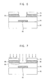
- a gate electrode 55 is formed on a substrate 50 including a transparent insulation material such as glass, quartz, transparent plastic, transparent ceramic, etc.
- the gate electrode 55 may be formed by a sputtering process, a spray process, a chemical vapor deposition (CVD) process, an atomic layer deposition (ALD) process, a vacuum evaporation process, a printing process, etc.
- the gate electrode 55 may be formed on the substrate 50 by patterning a first conductive layer after forming the first conductive layer on the substrate 50.
- a gate line may be formed on the substrate 50 while forming the gate electrode 55.
- the gate line may extend on the substrate 50 along a first direction
- the gate electrode 55 may extend from the gate line along a direction substantially perpendicular to the first direction.
- the gate electrode 55 may be formed using aluminum, tungsten, copper, nickel, chrome, molybdenum, titanium, platinum, tantalum, ruthenium, alloys containing these metals, nitrides containing these metals, a conductive metal oxide, etc. These may be used alone or in a combination thereof. Further, the gate electrode 55 may have a single layer structure or a multi layer structure. For example, the gate electrode 55 may have a single layer structure or a multi layer structure, which includes an electrically conductive material and/or a thermally resistive material. In some example embodiments, the gate electrode 55 may be obtained by patterning a transparent conductive material layer after forming the transparent conductive material layer on the substrate 50. The transparent conductive material film for the gate electrode 55 may be formed using indium tin oxide (ITO), indium zinc oxide (IZO), zinc oxide, tin oxide, gallium oxide, indium oxide, etc. These may be used alone or in combinations thereof.
- ITO indium tin oxide
- IZO indium
- a buffer layer is formed on the substrate 50, and then the gate electrode 55 is formed on the buffer layer.
- the buffer layer on the substrate 50 may have a single layer structure or a multi layer structure, which may include silicon oxide, silicon nitride and/or silicon oxynitride.
- the buffer layer may mitigate or prevent a diffusion of impurities from the substrate 50 while forming the gate electrode 55 and may improve a flatness of the substrate 50. Additionally, the buffer layer may reduce a stress generated between the substrate 50 and the gate electrode 55.
- a gate insulation layer 60 is formed on the substrate 50 to cover the gate electrode 55 in step S110.
- the gate insulation layer 60 may be obtained by a chemical vapor deposition process, a thermal oxidation process, a plasma enhanced chemical vapor deposition (PECVD) process, a high density plasma-chemical vapor deposition (HDP-CVD) process, a spin coating process, etc.
- the gate insulation layer 60 may be formed using a silicon compound, a metal oxide, etc.
- the gate insulation layer 60 may be obtained using silicon oxide, silicon oxynitride, hafnium oxide, zirconium oxide, aluminum oxide, tantalum oxide, etc. These may be used alone or in combinations thereof.
- an electrode layer 65 is formed on the gate insulation layer 60 in step S120.
- the electrode layer 65 may be formed on the gate insulation layer 60 using a metal, an alloy, a metal nitride, a conductive metal oxide, and/or a transparent conductive material by a sputtering process, a printing process, a vacuum evaporation process, a chemical vapor deposition process, an atomic layer deposition process, etc.
- an etch stop layer and/or a protection layer is formed between the gate insulation layer 60 and the electrode layer 65.
- the etch stop layer and/or the protection layer may be formed using oxide, nitride, oxynitride, semiconductor oxide, etc. These may be used alone or in combinations thereof.
- the etch stop layer and/or the protection layer may protect underlying structures including the gate electrode 55 and the gate insulation layer 60 while etching the electrode layer 65.
- a mask layer 70 is formed on the electrode layer 65 in step S130.
- the mask layer 70 is formed by coating photoresist onto the electrode layer 65 through a spin coating process.
- the mask layer 70 is formed using a material having a relatively high etching selectivity with respect to the electrode layer 65.
- the mask layer 70 may be formed using silicon oxide, silicon nitride, silicon oxynitride, etc. These may be used alone or in combinations thereof.
- the mask layer 70 may be formed by a chemical vapor deposition process, an atomic layer deposition process, a plasma enhanced chemical vapor deposition process, a high density plasma-chemical vapor deposition process, etc.
- the mask layer 70 may have a single layer structure or a multi layer structure including an oxide film, a nitride film and/or an oxynitride film.
- a mask pattern 75 is formed on the electrode layer 65 by partially etching the mask layer 70.
- the mask pattern 75 may expose a portion of the electrode layer 65 under which the gate electrode 55 is positioned.
- the mask pattern 75 may be formed by an exposure process and a developing process.
- the mask pattern 75 may be formed on the electrode layer 65 by a photolithography process.
- an area of a portion of the electrode layer 65 exposed by the mask pattern 75 may be substantially smaller than an area of the gate electrode 55.
- the source and drain electrodes 80 and 85 When the source and drain electrodes 80 and 85 are formed on the gate insulation layer 60, a portion of the gate insulation layer 60 under which the gate electrode 55 is located may be exposed. An area of a portion of the gate insulation layer 60 exposed between the source and drain electrodes 80 and 85 may be substantially smaller than an area of the gate electrode 55.
- the source electrode 80 and the drain electrode 85 may be spaced apart each other on the gate insulation layer 60 by a distance (e.g., a predetermined distance). In this case, end portions of the source and drain electrodes 80 and 85 may be partially overlap with end portions of the gate electrode 55, respectively.
- a plasma treatment is performed on the portion of the gate insulation layer 60 exposed between the source and drain electrodes 80 and 85 as indicated by arrows in FIG. 7 .
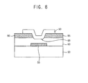
- a recess structure 68 may be formed on the gate insulation layer 60 by partially removing the gate insulation layer 60 during the plasma treatment as illustrated in FIG. 8 . That is, the plasma treatment may remove a portion of the gate insulation layer 60 having the etched damage, the internal stress, the residual stress and/or the etching by-products 88 remaining on a surface of the gate insulation layer 60.
- the recess structure 68 may have a depth of, for example, about 100 ⁇ to about 300 ⁇ based on (e.g., as measured from) the upper face of the gate insulation layer 65.
- the recess structure 68 may have a sidewall inclined by a relatively small angle of inclination in a range from about 10° to about 60° relative to a direction substantially perpendicular to the substrate 50.
- the plasma treatment may be executed using a plasma generated from a gas such as a gas including sulfur fluoride (SF x ), a gas including chlorine fluoride (ClF x ), a gas including hydrogen chloride (HCl), a gas including boron chloride (BCl x ), a gas including hydrocarbon (C x H y ), a gas including oxygen (O 2 ), a gas including ozone (O 3 ), etc.
- a gas including sulfur fluoride (SF x ) a gas including chlorine fluoride (ClF x ), a gas including hydrogen chloride (HCl), a gas including boron chloride (BCl x ), a gas including hydrocarbon (C x H y ), a gas including oxygen (O 2 ), a gas including
- the mask pattern 75 is removed from the source and drain electrodes 80 and 85 in step S170.
- the mask pattern 75 may be removed by a stripping process and/or an ashing process.
- the mask pattern 75 may be removed by using an etching solution phosphoric acid or hydrogen fluoride, or an etching gas including phosphoric acid or hydrogen fluoride.
- an active layer is formed on the source electrode 80, the drain electrode 85 and the gate insulation layer 60 having the recess structure 68.
- the active layer may be formed using a semiconductor oxide.
- the semiconductor oxide may include a binary compound (AB x ), a ternary compound (AB x C y ) or a quaternary compound (AB x C y D z ), which may contain indium (In), zinc (Zn), gallium (Ga), tin (Sn), titanium (Ti), etc.
- the active layer may be formed using the semiconductor oxide doped with additional elements such as lithium (Li), sodium (Na), manganese (Mn), nickel (Ni), palladium (Pd), copper (Cu), carbon (C), nitrogen (N), phosphorus (P), titanium (Ti), zirconium (Zr), vanadium (V), ruthenium (Ru), germanium (Ge), tin (Sn), fluorine (F), etc. These may be added alone or in combinations thereof.
- the active layer includes amorphous silicon, polysilicon, partially crystallized silicon, silicon containing micro crystals, etc.
- the active layer may be formed by a sputtering process, a spray process, a chemical vapor deposition (CVD) process, an atomic layer deposition (ALD) process, a vacuum evaporation process, a printing process, a sol-gel process, a plasma enhanced chemical vapor deposition (PECVD) process, etc.
- a carrier concentration of the active layer may be in a range from about 1 x 10 12 atoms/cm 3 to about 1 x 10 18 atoms/cm 3 .
- An active pattern 90 is formed on the gate insulation layer 60, the source electrode 80 and the drain electrode 85 by partially etching the active layer in step S180.
- an oxide semiconductor device including the gate electrode 55, the gate insulation layer 60 having the recess structure 68, the source electrode 80, the drain electrode 85 and the active pattern 90 may be provided on the substrate 50.
- the active pattern 90 may be obtained by a photolithography process or an etching process using an additional etching mask.
- the active pattern 90 may have stepped portions adjacent to the source and drain electrodes 80 and 85 because the active pattern 90 may be formed along profiles of the source electrode 80, the drain electrode 85 and the gate insulation layer 60 having the recess structure 68.
- a first portion of the active pattern 90 may extend on the source electrode 80
- a second portion of the active pattern 90 may extend on the drain electrode 85.
- an upper portion of the active pattern 90 may have an area substantially larger than that of the gate electrode 55
- a lower portion of the active pattern 90 may have an area substantially smaller than that of the gate electrode 55.
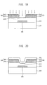
- FIG. 9 is a flow chart illustrating a method of manufacturing an oxide semiconductor device in accordance with some example embodiments of the present invention.
- FIGS. 10 to 12 are cross-sectional views illustrating a method of manufacturing an oxide semiconductor device in accordance with some example embodiments of the present invention.
- the method may provide an oxide semiconductor device having a construction substantially the same as or substantially similar to that of the oxide semiconductor device described with reference to FIG. 1 , however, the method illustrated in FIGS. 9 to 12 may be employed in manufacturing other oxide semiconductor devices having various constructions including gate electrodes, gate insulation layers, active patterns, source electrodes, drain electrodes, etc.
- a gate electrode 105 is formed on a substrate 100 including a transparent insulation material in step S200, and then a gate insulation layer 110 is formed on the substrate 100 to cover the gate electrode 105 in step S210.
- the gate electrode 105 may be formed using a metal, an alloy, a conductive metal oxide, a transparent conductive material, etc.
- the gate insulation layer 110 may be formed using a silicon compound, a metal oxide, etc.
- the gate insulation layer 110 may have a substantially level upper face while sufficiently covering the gate electrode 105. In this case, a planarization process may be additionally performed on an upper portion of the gate insulation layer 110.
- An electrode layer 115 is formed on the gate insulation layer 110 in step S220.
- the electrode layer 115 may include a metal, an alloy, a metal nitride, a conductive metal oxide, and/or a transparent conductive material.
- the electrode layer 115 may have a single layer structure or a multi layer structure. In example embodiments of the present invention, when the gate insulation layer 110 has a substantially level upper face, the electrode layer 115 may also have a substantially flat upper face due to the substantially flat upper face of the gate insulation layer 110.
- a mask pattern 120 is formed on the electrode layer 115 in step S230.
- the mask pattern 120 may be formed using photoresist, silicon oxide, silicon nitride, silicon oxynitride, etc.
- the mask pattern 120 may expose a portion of the electrode layer 115 under which the gate electrode 105 is positioned. In this case, an area of a portion of the electrode layer 115 exposed by the mask pattern 120 may be substantially smaller than an area of the gate electrode 105.
- the electrode layer 115 is patterned using the mask pattern 120 as an etching mask, so that a source electrode 125 and a drain electrode 130 is formed on the gate insulation layer 110 in step S240.
- the source electrode 125 and the drain electrode 130 may be separated from each other on the gate insulation layer 110 by a distance (e.g., a predetermined distance).
- a distance e.g., a predetermined distance.
- the portion of the gate insulation layer 110 exposed between the source and drain electrodes 125 and 130 may be damaged during an etching process for removing a portion of the electrode layer 115. Further, the gate insulation layer 110 may have a residual stress, an internal stress and/or etching by-products 128 including metal compounds, metallic particles.
- an interface between the gate insulation layer 110 and the active pattern may be deteriorated. In case that the interface between the gate insulation layer 110 and the active pattern is damaged or deteriorated, a channel region of the oxide semiconductor device may be irregular and characteristics of the oxide semiconductor device may also be deteriorated.
- a cleaning treatment is performed on the portion of the gate insulation layer 110 exposed between the source and drain electrodes 125 and 130 as indicated by an arrow in FIG. 11 .
- a recess structure 118 is formed on the gate insulation layer 110 by partially removing a portion of the exposed gate insulation layer 110 with the cleaning treatment. That is, the cleaning treatment may remove a portion of the gate insulation layer 110 having the etched damage, the internal stress, the residual stress and/or the etching by-products, so that the recess structure 118 having a depth (e.g., a predetermined depth) may be provided on the gate insulation layer 110 substantially without defects as illustrated in FIG. 12 .
- a depth e.g., a predetermined depth
- the cleaning treatment is carried out using a mixture including a solution for removing a metal compound and a pure water or a deionized water.
- the cleaning treatment may be executed using a solution such as a solution including hydrogen fluoride, a solution including hydrogen chloride, a solution including phosphoric acid, a solution including potassium hydroxide, a solution including hydrogen bromide, a solution including iodine bromide, etc. These may be used alone or in combinations thereof.
- FIG. 13 is a flow chart illustrating a method of manufacturing an oxide semiconductor device in accordance with some example embodiments of the present invention.
- the method of manufacturing illustrated in FIG. 13 may include processes substantially the same as or substantially similar to those of the method described with reference to FIG. 2 except for a plasma treatment and a cleaning treatment for a gate insulation layer.
- a mask pattern is formed on the electrode layer in step S330.
- the electrode layer may have a substantially level upper face substantially caused by that of the gate insulation layer.
- the mask pattern may expose a portion of the electrode layer under which the gate electrode is located.
- the electrode layer is patterned using the mask pattern as an etching mask, such that a source electrode and a drain electrode is formed on the gate insulation layer in step S340.
- the source electrode and the drain electrode may be separated each other on the gate insulation layer by a distance (e.g., a predetermined distance) substantially centered around the gate electrode. Hence, a portion of the gate insulation layer between the source electrode and the drain electrode may be exposed. The portion of the gate insulation layer exposed between the source and drain electrodes may be damaged during an etching process for etching a portion of the electrode layer.
- the gate insulation layer may have a residual stress, an internal stress and/or etching by-products including metal compounds and/or metallic particles after the etching process for forming the source and drain electrodes.
- a plasma treatment is performed on the gate insulation layer in step S350.
- the portion of the gate insulation layer between the source and drain electrodes may be primarily removed by the plasma treatment, so that a preliminary recess structure is formed on the gate insulation layer.
- the preliminary recess structure may have a depth substantially smaller than or substantially similar to that of the recess structure 18 described with reference to FIG. 1 by controlling process conditions of the plasma treatment such as a time (e.g., length of time) of treating a plasma, a flow of a gas generating a plasma, etc.
- the plasma treatment may primarily remove damaged portions of the gate insulation layer and etching by-products remaining on the gate insulation layer. For example, the damaged portions and the etching by-products of the gate insulation layer may be partially removed or completely removed by the plasma treatment.
- an active pattern is formed on the gate insulation layer, the source electrode and the drain electrode by patterning the active layer using a photolithography process or an etching process using an additional etching mask. Therefore, an oxide semiconductor device having a construction substantially the same as or substantially similar to that of the oxide semiconductor device described with reference to FIG. 1 may be provided on the substrate. In this case, the active pattern may have stepped portions adjacent to the source and drain electrodes.
- FIG. 14 is a flow chart illustrating a method of manufacturing an oxide semiconductor device in accordance with some example embodiments of the present invention.
- the method of manufacturing an oxide semiconductor device illustrated in FIG. 14 may include processes substantially the same as or substantially similar to those of the method of manufacturing an oxide semiconductor device described with reference to FIG. 2 except for a plasma treatment and a cleaning treatment of a gate insulation layer.
- the electrode layer may be partially etched using the mask pattern as etching mask, and thus a source electrode and a drain electrode are respectively formed on a first portion and a second portion of the gate insulation layer in step S440.
- the source electrode and the drain electrode may be spaced apart on the gate insulation layer by a distance substantially the same as or substantially similar to a length of a channel region of the oxide semiconductor device.
- the mask pattern is removed from the source and drain electrodes in step S460.
- the mask pattern may be removed by a dry etching process or a wet etching process.
- a cleaning treatment is performed on the gate insulation layer having the preliminary recess structure in step S470.
- the cleaning treatment may be substantially the same as or substantially similar to the cleaning treatment described with reference to FIG. 9 .
- the damaged and stressed portion of the gate insulation layer and the etching by-products may be completely removed by the cleaning treatment.
- a recess structure may be provided on a portion the gate insulation layer between the source and drain electrodes by substantially extending a size (e.g., the depth) of the preliminary recess structure through the cleaning treatment.
- damage to the gate insulation layer may be additionally caused while removing the mask pattern or etching by-products from the mask pattern may be additionally be left on the gate insulation layer
- the damaged portion and the etching by-products may be efficiently removed from the gate insulation layer by the cleaning treatment which may be carried out after removing the mask pattern.
- An active pattern is formed on the source electrode, the drain electrode and the gate insulation layer having the recess structure in step S480.
- the active pattern may be formed on the gate insulation layer, the source electrode and the drain electrode by partially etching the active layer with a photolithography process or an etching process using an additional etching mask.
- an oxide semiconductor device having a construction substantially the same as or substantially similar to that of the oxide semiconductor device described with reference to FIGS. 1 or 8 may be provided on the substrate.
- the cleaning treatment may be performed on the plasma-treated gate insulation layer after removing the mask pattern, the damage to the gate insulation layer and the etching by-products remaining on the gate insulation layer may be completely removed. Further, the additional damaged portions of the gate insulation layer and the additional etching by-products remaining on the gate insulation layer may be effectively removed by the cleaning treatment. Therefore, the oxide semiconductor device may exhibit further improved electrical characteristics by enhancing uniformity and flatness of the channel region of the oxide semiconductor device.
- FIG. 15 is a cross-sectional view illustrating an oxide semiconductor device in accordance with some example embodiments of the present invention.
- the oxide semiconductor device in FIG. 15 may have a construction substantially the same as or substantially similar to that of the oxide semiconductor device described with reference to the embodiment of FIG. 1 except structures of a source electrode 175 and a drain electrode 190.
- the oxide semiconductor device includes a gate electrode 155, a gate insulation layer 160 having a recess structure 168, a source electrode 175, a drain electrode 190 and an active pattern 195.
- the recess structure 168 may be provided on (or above) the gate insulation layer 160, and the active pattern 195 may be disposed on the source and drain electrodes 175 and 190 to fill the recess structure 168.
- the recess structure 168 has a size and a shape substantially the same as or substantially similar to the size and shape of the recess structure 18 described with reference to FIG. 1 .
- the source electrode 175 may have a first electrode pattern 165 and a second electrode pattern 170
- the drain electrode 190 may have a third electrode pattern 180 and a fourth electrode pattern 185.
- Each of the first and third electrode patterns 165 and 180 may include a metal, an alloy, a transparent conductive material, etc.
- Each of the second and the fourth electrode patterns 170 and 185 may include a metal nitride, a metal oxide, etc.
- the first and the third electrode patterns 165 and 180 may include chrome, aluminum, copper, molybdenum, titanium, tantalum, tungsten, neodymium, scandium, alloy of these metals, strontium ruthenium oxide, indium tin oxide, indium zinc oxide, zinc oxide, tin oxide, carbon nanotubes, etc. These may be used alone or in combinations thereof.
- each of the second and the fourth electrode patterns 170 and 185 may include a metal nitride and/or a nitride of a transparent conductive material resulting from the first and the third electrode patterns 165 and 180.
- the second and the fourth electrode patterns 170 and 185 may include chrome nitride (CrN x ), aluminum nitride (AlN x ), titanium nitride (TiN x ), tantalum nitride (TaN x ), tungsten nitride (WN x ), molybdenum nitride (MoN x ), neodymium nitride (NdN x ), scandium nitride (ScN x ), ruthenium nitride (RuN x ), nitrides of alloys containing these metals, strontium ruthenium oxynitride, indium tin oxynitride, indium zinc oxynitride, zinc oxynitride, tin oxynitride, carbon nanotube nitride, etc.
- CrN x chrome nitride
- AlN x aluminum n
- the second and the fourth electrode patterns 170 and 185 include a metal nitride or a nitride of a transparent conductive material
- the first and the third electrode patterns 165 and 180 may be effectively protected while successively performing a plasma treatment and/or a cleaning treatment.
- electrical characteristics of the oxide semiconductor device may be enhanced by preventing or mitigating additional damage or deterioration of the source and drain electrodes 175 and 190.
- a gate electrode 205 is formed on a substrate 200 in step S500, and then a gate insulation layer 210 is formed on the gate electrode 205 and the substrate 200 in step S510.
- the gate insulation layer 210 may have a substantially level upper face.
- a second electrode film 220 is formed on the first electrode 215 in step S530.
- an electrode layer 225 including the first and the second electrode films 215 and 220 may be provided on the gate insulation layer 210.
- the first electrode film 215 may be formed using a metal, an alloy, a transparent conductive material, etc.
- the first electrode film 215 may be formed using chrome, aluminum, molybdenum, titanium, tantalum, tungsten, neodymium, scandium, ruthenium, alloy of these metals, strontium ruthenium oxide, indium tin oxide, indium zinc oxide, zinc oxide, tin oxide, carbon nanotubes, etc. These may be used alone or in combinations thereof.
- the first electrode film 215 may be formed on the gate insulation layer 210 by a sputtering process, a spray process, a chemical vapor deposition process, an atomic layer deposition process, a vacuum evaporation process, a printing process, etc.
- the second electrode film 220 may be formed by performing a nitration treatment on the first electrode film 215. That is, a portion of the first electrode film 215 may be changed into the second electrode film 220 by nitriding the first electrode film 215.
- the nitration treatment may include thermally treating the first electrode film 215 under an atmosphere containing nitrogen.
- the atmosphere containing nitrogen may include nitrogen (N 2 ), nitric oxide (NO), nitrous oxide (N 2 O), nitrogen dioxide (NO 2 ), ammonia (NH 3 ), etc. These may be used alone or in combinations thereof.
- the nitration treatment may include treating the first electrode film 215 with a plasma generated from a gas containing nitrogen.
- the gas for generating the plasma may include nitrogen, nitric oxide, nitrous oxide, nitrogen dioxide, ammonia, etc. These may be used alone or in combinations thereof.
- etching by-products 248 may remain on the gate insulation layer 210 while etching the electrode layer 225 to form the source and drain electrode 245 and 260. Additionally, the gate insulation layer 210 may be damaged in an etching process for the electrode layer 225 and may also have a residual stress or an internal stress therein.
- etching damage to the first and the third electrode patterns 235 and 250 may be effectively protected against or reduced because the first and the third electrode patterns 235 and 250 are protected by the second and the fourth electrode patterns 240 and 255.
- an active layer 265 is formed on the source electrode 245, the drain electrode 260 and the gate insulation layer 210 having the recess structure 218. That is, the active layer 265 filling the recess structure 218 may be formed on the gate insulation layer 210, the second electrode pattern 240 and the fourth electrode pattern 255.
- an active pattern is formed on the gate insulation layer 210, the source electrode 245 and the drain electrode 260 by a photolithography process or an etching process using an additional etching mask.
- the active pattern may completely fill the recess structure 218.
- an oxide semiconductor device having a construction substantially the same as or substantially similar to that of the oxide semiconductor device described with reference to FIG. 15 may be provided on the substrate 200.
- FIG. 21 is a cross-sectional view illustrating an oxide semiconductor device in accordance with some example embodiments of the present invention.
- the gate insulation layer 290 may be uniformly formed on a substrate 280 along a profile of the gate electrode 285.
- the gate insulation layer 290 may include stepped portions adjacent to end portions of the gate electrode 285, respectively.
- the gate insulation layer 290 may have a substantially small thickness.
- the gate insulation 290 may have a thickness of about 500 ⁇ to about 1,000 ⁇ based on an upper face of the gate electrode 285.
- each element of the oxide semiconductor device may also have a structure including a stepped portion.
- the recess structure 298 may be located on the gate insulation layer 290.
- the recess structure 298 may have a construction substantially the same as or substantially similar to that of the recess structure 18 described with reference to FIG. 1 .
- the recess structure 298 may have a depth of about 100 ⁇ to about 300 ⁇ .
- a ratio between the depth of the recess structure 298 and the thickness of the gate insulation layer 290 may be in a range from about 1.0:1.7 to about 1.0:10.0. That is, when the gate insulation layer 290 includes a stepped portion, the ratio between depth of the recess structure 298 and the thickness of the gate insulation layer 290 may be reduced.
- the recess structure 298 may include an inclined sidewall having a relatively small first angle of inclination with respect to an axis or a line substantially perpendicular to the substrate 280.
- Each of the source electrode 300 and the drain electrode 305 may be positioned on the gate insulation layer 290 having the recess structure 298.
- the source electrode 300 and the drain electrode 305 may be spaced apart by a distance substantially corresponding to a width of the recess structure 298.
- the source and drain electrodes 300 and 305 include stepped portions corresponding to the stepped portions of the gate insulation layer 290.
- each of the source and drain electrodes 300 and 305 may include a stepped portion adjacent to the stepped portion of the gate insulation layer 290.
- each of the source and drain electrodes 300 and 305 may have a relatively large second angle of inclination with respect to the axis, the line or the direction substantially perpendicular to the gate electrode 285.
- each of the source and drain electrodes 300 and 305 may have a construction substantially the same as or substantially similar to that of the source and drain electrodes 175 and 190 described with reference to FIG. 15 .
- the active pattern 310 may be disposed on the source and drain electrodes 300 and 305 to fill the recess structure 298.
- the active pattern 310 on the gate insulation layer 290 may contact a sidewall of the recess structure 298 and sidewalls of the source and drain electrodes 300 and 305.
- a lower portion of the active pattern 310 may have an inclined sidewall having a relatively small first inclined angle
- a central portion of the active pattern 310 may have an inclined sidewall having a relatively large second inclined angle.
- the active pattern 310 contacting the gate insulation layer 290 may be disposed on the source and drain electrodes 300 and 305, the active pattern 310 may include stepped portions adjacent to the stepped portions of the gate insulation layer 290.
- end portions of the active pattern 310 may extend on the source electrode 300 and the drain electrode 305, respectively.
- the active pattern 310 may have additional stepped portions respectively adjacent to the stepped portions of the source and drain electrodes 300 and 305.
- the active pattern 310 filling the recess structure 298 may have a substantially double-stepped structure.
- FIGS. 22 and 23 are cross-sectional views illustrating a method of manufacturing an oxide semiconductor device in accordance with some example embodiments of the present invention.
- the method may provide an oxide semiconductor device having a construction substantially the same as or substantially similar to that of the oxide semiconductor device described with reference to FIG. 21 , however, the method illustrated in FIGS. 22 to 23 may be employed in manufacturing other oxide semiconductor devices having various constructions including gate electrodes, gate insulation layers, active patterns, source electrodes, drain electrodes, etc.
- a gate electrode 335 is formed on a substrate 330 including a transparent insulation material.
- the gate electrode 335 is formed by patterning a conductive layer after forming the conductive layer on the substrate 330.
- the gate electrode 335 may be formed by a sputtering process, a chemical vapor deposition process, an atomic layer deposition process, a vacuum evaporation process, a printing process, etc.
- a buffer layer may be additionally formed on the substrate 330 before forming the gate electrode 335.
- a gate insulation layer 340 is formed on the gate electrode 335 and the substrate 330.
- the gate insulation layer 340 may be uniformly formed on a substrate 330 along a profile of the gate electrode 335.
- the gate insulation layer 340 may include stepped portions adjacent to the gate electrode 335. For example, stepped portions may be formed over portions of the gate insulation layer 340 adjacent to both end portions of the gate electrode 335.
- the gate insulation layer 340 having a relatively small thickness may be formed using a silicon compound and/or a metal oxide.
- An electrode layer 345 is formed on the gate insulation layer 340.
- the electrode layer 345 may be conformally formed on the gate insulation layer 340 along a profile of the gate electrode 335.
- the electrode layer 345 may also have stepped portions adjacent to the stepped portions of the gate insulation layer 340.
- the electrode layer 345 may have a construction substantially the same as or substantially similar to that of the electrode layer 225 described with reference to FIG. 17 .
- a mask pattern 350 is formed on the electrode layer 345.
- the mask pattern 350 may be formed using photoresist, an oxide, a nitride, an oxynitride, etc. Further, the mask pattern 350 may have a single layer structure or a multi layer structure.
- the electrode layer 345 may be partially etched using the mask pattern 350. Accordingly, a source electrode 360 and a drain electrode 365 may be formed on a first portion and a second portion of the gate insulation layer 340, respectively.
- the source electrode 360 and the drain electrode 365 have stepped portions adjacent to the stepped portions of the gate insulation layer 340, respectively. Due to the shapes of the source and drain electrodes 360 and 365, a portion of gate insulation layer 340 between the source and drain electrodes 360 and 365 may be exposed. The exposed portion of the gate insulation layer 340 may be damaged during an etching process for patterning the electrode layer 345 to form the source and drain electrodes 360 and 365. Further, the gate insulation layer 340 may have a residual stress, an internal stress and/or etching by-products remaining thereon.
- An active pattern may be formed on the gate insulation layer 340, the source electrode 360 and the drain electrode 365, such that the oxide semiconductor device may be formed on the substrate 330.
- the oxide semiconductor device may have a construction substantially the same as or substantially similar to that of the oxide semiconductor device described with reference to FIG. 21 .
- a gate electrode was formed on a substrate, and then a gate insulation layer was formed on the substrate to cover the gate electrode. After forming an electrode layer on the gate insulation layer, a source electrode and a drain electrode were formed on the gate insulation layer by patterning the electrode layer. A plasma treatment was performed on the gate insulation layer between the source and drain electrodes using a plasma generated from a mixture of sulfur hexafluoride (SF 6 ) and oxygen (O 2 ). A recess structure was formed on the gate insulation layer by the plasma treatment. An active pattern was formed on the gate insulation layer, the source electrode and the drain electrode, thereby obtaining an oxide semiconductor device.
- SF 6 sulfur hexafluoride
- O 2 oxygen
- a gate electrode was formed on a substrate, and then a gate insulation layer was formed on the substrate to cover the gate electrode. After forming an electrode layer on the gate insulation layer, a source electrode and a drain electrode were formed on the gate insulation layer by patterning the electrode layer. A cleaning treatment was performed on the gate insulation layer between the source and drain electrodes using a solution including hydrogen fluoride. A recess structure was formed on the gate insulation layer by the cleaning treatment. An active pattern was formed on the gate insulation layer, the source electrode and the drain electrode, so that an oxide semiconductor device was provided on the substrate.
- Table shows measured results of charge mobilities and variation of threshold voltages of oxide semiconductor devices according to Examples 1 to 3 and Comparative Example.
- Table Comparative Example Example 1 Example 2
- Example 3 charge mobility 4.10 cm 2 /Vs 8.20 cm 2 /Vs 4.55 cm 2 /Vs 8.43 cm 2 /Vs variation of threshold voltages 0.98 V/decade 0.78 V/decade 0.83 V/decade 0.78 V/decade
- the charge mobility of the oxide semiconductor devices are increased by about 1.73 times on average, while the variation of threshold voltages of the oxide semiconductor devices are decreased by about 18.7% on average, comparing with Comparative Example in which the plasma treatment and/or the cleaning treatment is not carried out.
- the charge mobility of the oxide semiconductor device greatly increases and the variation of threshold voltages of the oxide semiconductor device considerably decreases. Therefore, electrical characteristics of the oxide semiconductor device may be improved when the plasma treatment and/or the cleaning treatment is performed on the gate insulation layer of the oxide semiconductor device.
- the active pattern 430 is disposed on the gate insulation layer 415, the source electrode 420 and the drain electrode 425 to fill the recess structure 418.
- a lower portion of the active pattern 430 may have a relatively small first inclined angle with respect to an axis, a line or a direction substantially perpendicular to the substrate 400.
- a central portion of the active pattern 430 may have a relatively large second inclined angle relative to the axis, the line or the direction substantially perpendicular to the gate electrode 405.
- the light emitting structure is positioned on the insulation layer 435.
- the light emitting structure may include a first electrode 440, the light emitting layer 450 and a second electrode 455.
- the first and the second electrodes 440 and 455 may include transparent conductive materials, transflective conductive materials or reflective conductive materials according to an emission type of the display device.
- the display device may be a top emission type, a bottom emission type or a dual emission type display in accordance with materials included in the first and the second electrodes 440 and 455.
- a pixel defining layer 445 is disposed on the insulation layer 435 covering the oxide semiconductor device. That is, the pixel defining layer 445 is positioned on a portion of the insulation layer 435 covering the oxide semiconductor device. In this case, the pixel defining layer 445 may extend to a region in which the drain electrode 425 is connected to the first electrode 440. The pixel defining layer 445 may divide adjacent pixels of the display device.
- the pixel defining layer 445 may include an insulation material.
- the pixel defining layer 445 may include polyacryl-based resin, polyimide-based resin, a silica-based inorganic material, etc.
- An opening is formed through the pixel defining layer 445 to expose a portion of the first electrode 440.
- the light emitting layer 450 and the second electrode 455 of the light emitting structure is uniformly disposed on the exposed portion of the first electrode 440, a sidewall of the opening and the pixel defining layer 445 along a profile of the opening.
- a plurality of openings is provided through the pixel defining layer 445 in a plurality of pixels of the display device.
- Each of the openings may partially expose a portion of first electrode 440 in each pixel.
- the first electrode 440 is disposed only in the opening of the pixel defining layer 445.
- the first electrode 440 may extend beneath the pixel defining layer 310, so that the first electrode 440 is partially overlapped relative to the pixel defined layer 445.
- a region including the pixel defining layer 445 may substantially correspond to a non-luminescent region of the display device, and another region having the opening of the pixel defining layer 445 may substantially correspond to a luminescent region of the display device.
- the second substrate 465 may not be provided on the protection layer 460 in accordance with a construction of the protection layer 460 and/or a material of the protection layer 460.
- the protection layer 460 may be omitted according to a construction of the second substrate 465 and/or a material in the second substrate 460.
- the display device may include the oxide semiconductor device having improved electrical characteristics such as an increased operation current, a reduced threshold voltage variation, an increased charge mobility in a channel region, etc. Therefore, a thickness of the display device may be reduced, and a resolution of image displayed by the display device may be improved. Further, the display device may ensure an improved display speed and a high quality of image.
- a gate electrode 505 and a gate line 510 is formed on a first substrate 500.
- the gate electrode 505 and the gate line 510 may be formed on the first substrate 500 by partially etching the conductive layer through a photolithography process.
- a source electrode 520 and a drain electrode 525 is formed on the gate insulation layer 515 by patterning the electrode layer 517.
- the source and drain electrodes 520 and 525 may be separated each other on the gate insulation layer 515 substantially centered around the gate electrode 505.
- the drain electrode 525 may extend on a portion of the gate insulation layer 515 under which the gate line 510 is located.
- the gate insulation layer 515 may be damaged in an etching process for forming the source and drain electrodes 520 and 525. Further, etching by-products may remain on the gate insulation layer 515 after the etching process. Thus, a recess structure 515 may be formed on the gate insulation layer 515 by performing a plasma treatment and/or a cleaning treatment on the gate insulation layer 515 to remove the damage to the gate insulation layer 515 and the etching by-products remaining on the gate insulation layer 515. As described above, the gate insulation layer 515 may have a recess structure 518 after the plasma treatment and/or the cleaning treatment.
- An insulation layer 535 is formed on the first substrate 500 to cover the oxide semiconductor device.
- the insulation layer 535 may be formed using a transparent insulation material.
- the insulation layer 535 may have a substantially level upper face. In this case, an upper portion of the insulation layer 535 may be planarized by a planarization process such as a chemical mechanical polishing process, an etch-back process, etc.
- a hole is formed through the insulation layer 535 to expose a portion of the drain electrode 525 of the oxide semiconductor device.
- the hole of the insulation layer 535 may be obtained by a photolithography process.
- a first electrode layer may be formed on the exposed portion of the drain electrode 525, a sidewall of the hole of the insulation layer 535 and the insulation layer 535.
- the first electrode layer may be uniformly formed on the drain electrode 525 and the insulation layer 535 along a profile of the hole of the insulation layer 535.
- the first electrode layer may be formed using a transparent conductive material, a transflective conductive material, a reflective conductive material, etc.
- a first electrode 540 may be obtained by patterning the first electrode layer.
- the first electrode 540 may serve as a pixel electrode of the display device.
- the first electrode 540 may be formed on the exposed portion of the drain electrode 525, a sidewall of the hole of the insulation layer 535 and the insulation layer 535.
- the first electrode 540 may not be positioned on a portion of the insulation layer 535 under which the oxide semiconductor device is located.
- a contact structure or a pad structure is formed on the exposed portion of the drain electrode 525 in the hole, so that the first electrode 540 is electrically connected to the oxide semiconductor device through the contact structure or the pad structure.
- a pixel defining layer 545 is formed on the insulation layer 535 and the first electrode 540.
- the pixel defining layer 545 may be formed using an insulation material.
- the pixel defining layer 545 may be formed using polyacryl-based resin, polyimide-based resin, a silica-based inorganic material, etc.
- An opening is formed through the pixel defining layer 545 by partially etching the pixel defining layer 545, such that a portion of the first electrode 540 is exposed by the opening.
- the opening may be obtained by a photolithography process.
- the opening of the pixel defining layer 545 may include an inclined sidewall having an angle (e.g., a predetermined angle) relative to the first substrate 500.
- a light emitting layer 550 and/or a second electrode 555 may be easily formed on the first electrode 540 and the pixel defining layer 545 along the inclined sidewall of the opening of the pixel defining layer 545.
- the light emitting layer 550 is formed on the first electrode 540, the sidewall of the opening and the pixel defining layer 545.
- the light emitting layer 550 may be uniformly formed on the exposed portion of the first electrode 540, the sidewall of the opening and the pixel defining layer 545 along a profile of the opening.
- the light emitting layer 550 may be formed using an organic material having a relatively small molecular weight, an organic material having a relatively large molecular weight, etc.
- the light emitting layer 550 may have a multi layer structure that includes an organic light emitting layer, a hole injection layer, a hole transport layer, an electron injection layer, an electron transport layer, etc.
- a second electrode 555 is formed on the light emitting layer 550.
- the second electrode 555 may be formed using a transparent conductive material, a transflective conductive material, a reflective conductive material, etc.
- the second electrode 555 may be uniformly formed on the light emitting layer 550.
- the second electrode 555 may also be formed in the opening of the pixel defining layer 545 only.
- the light emitting layer 550 may be formed on the first electrode 540 and the sidewall of the opening, and the second electrode 555 may be formed on such light emitting layer 500.
- the second electrode 555 may be obtained by pattering the second electrode layer.
- a protection layer 560 is formed on the second electrode 550.
- the protection layer 560 may be formed a transparent insulation material such as glass, quarts, transparent plastic, transparent ceramic, etc.
- a second substrate substantially corresponding to the first substrate 500 may be provided on the protection layer 560.
- the second substrate may include a transparent insulation material.
- an oxide semiconductor device including a gate insulation layer having a recess structure may be employed in various display devices such as an organic light emitting display device, a liquid crystal display device, a flexible display device, etc. Therefore, the display device including the oxide semiconductor device may ensure a high quality of image and a high display speed while reducing a whole thickness of the display device.
Landscapes
- Engineering & Computer Science (AREA)
- Thin Film Transistor (AREA)
- Manufacturing & Machinery (AREA)
- Physics & Mathematics (AREA)
- Microelectronics & Electronic Packaging (AREA)
- Computer Hardware Design (AREA)
- General Physics & Mathematics (AREA)
- Power Engineering (AREA)
- Condensed Matter Physics & Semiconductors (AREA)
- Electroluminescent Light Sources (AREA)
- Plasma & Fusion (AREA)
- Chemical & Material Sciences (AREA)
- Chemical Kinetics & Catalysis (AREA)
- General Chemical & Material Sciences (AREA)
Applications Claiming Priority (1)
| Application Number | Priority Date | Filing Date | Title |
|---|---|---|---|
| KR1020110046116A KR101830170B1 (ko) | 2011-05-17 | 2011-05-17 | 산화물 반도체 소자, 산화물 반도체 소자의 제조 방법, 산화물 반도체소자를 포함하는 표시 장치 및 산화물 반도체 소자를 포함하는 표시 장치의 제조 방법 |
Publications (2)
| Publication Number | Publication Date |
|---|---|
| EP2525408A1 true EP2525408A1 (de) | 2012-11-21 |
| EP2525408B1 EP2525408B1 (de) | 2016-12-21 |
Family
ID=45033871
Family Applications (1)
| Application Number | Title | Priority Date | Filing Date |
|---|---|---|---|
| EP11190716.8A Active EP2525408B1 (de) | 2011-05-17 | 2011-11-25 | Verfahren zur Herstellung der Oxidhalbleitervorrichtungen, Verfahren zur Herstellung der Anzeigevorrichtungen mit den Oxidhalbleitervorrichtungen |
Country Status (6)
| Country | Link |
|---|---|
| US (2) | US20120292610A1 (de) |
| EP (1) | EP2525408B1 (de) |
| JP (1) | JP5905692B2 (de) |
| KR (1) | KR101830170B1 (de) |
| CN (1) | CN102820330A (de) |
| TW (1) | TWI562286B (de) |
Cited By (2)
| Publication number | Priority date | Publication date | Assignee | Title |
|---|---|---|---|---|
| GB2534313B (en) * | 2013-12-27 | 2021-03-24 | Shenzhen China Star Optoelect | Array substrate and liquid crystal display panel using same |
| JP2024071433A (ja) * | 2014-02-05 | 2024-05-24 | 株式会社半導体エネルギー研究所 | 半導体装置 |
Families Citing this family (36)
| Publication number | Priority date | Publication date | Assignee | Title |
|---|---|---|---|---|
| US8829528B2 (en) * | 2011-11-25 | 2014-09-09 | Semiconductor Energy Laboratory Co., Ltd. | Semiconductor device including groove portion extending beyond pixel electrode |
| JP6033071B2 (ja) * | 2011-12-23 | 2016-11-30 | 株式会社半導体エネルギー研究所 | 半導体装置 |
| KR101968115B1 (ko) * | 2012-04-23 | 2019-08-13 | 엘지디스플레이 주식회사 | 어레이 기판 및 이의 제조방법 |
| US9305939B2 (en) * | 2012-06-08 | 2016-04-05 | Sharp Kabushiki Kaisha | Semiconductor device with oxide layer as transparent electrode |
| KR102227591B1 (ko) * | 2012-10-17 | 2021-03-15 | 가부시키가이샤 한도오따이 에네루기 켄큐쇼 | 반도체 장치 |
| WO2014082292A1 (zh) * | 2012-11-30 | 2014-06-05 | 深圳市柔宇科技有限公司 | 自对准金属氧化物薄膜晶体管器件及制造方法 |
| CN103258859B (zh) * | 2013-05-23 | 2016-06-29 | 北京交通大学 | 一种氧化铟基薄膜晶体管及其制作方法 |
| JP6426379B2 (ja) * | 2013-06-19 | 2018-11-21 | 株式会社半導体エネルギー研究所 | 半導体装置の作製方法 |
| KR101466832B1 (ko) * | 2013-06-28 | 2014-11-28 | 코닝정밀소재 주식회사 | 유기발광소자 |
| TWM471031U (zh) | 2013-08-13 | 2014-01-21 | Chunghwa Picture Tubes Ltd | 氧化物半導體薄膜電晶體基板 |
| CN103744224A (zh) * | 2013-12-27 | 2014-04-23 | 深圳市华星光电技术有限公司 | 阵列基板及用该阵列基板的液晶显示面板 |
| CN103744225B (zh) * | 2013-12-27 | 2016-08-17 | 深圳市华星光电技术有限公司 | 阵列基板及用该阵列基板的液晶显示面板 |
| CN103744240A (zh) * | 2013-12-27 | 2014-04-23 | 深圳市华星光电技术有限公司 | 阵列基板及用该阵列基板的液晶显示面板 |
| KR102266700B1 (ko) | 2014-07-09 | 2021-06-22 | 삼성디스플레이 주식회사 | 박막 트랜지스터 제조방법 및 박막 트랜지스터를 포함하는 표시기판 제조방법 |
| US10287499B2 (en) * | 2014-10-10 | 2019-05-14 | Kanto Denka Kogyo Co., Ltd. | Etching gas composition for silicon compound, and etching method |
| CN104795449B (zh) * | 2015-04-16 | 2016-04-27 | 京东方科技集团股份有限公司 | 薄膜晶体管及制作方法、阵列基板、显示装置 |
| JP6457896B2 (ja) * | 2015-07-09 | 2019-01-23 | 株式会社ジャパンディスプレイ | 半導体装置及び半導体装置の製造方法 |
| US10050152B2 (en) * | 2015-12-16 | 2018-08-14 | Semiconductor Energy Laboratory Co., Ltd. | Transistor, semiconductor device, and electronic device |
| CN105702586B (zh) * | 2016-04-28 | 2019-06-07 | 京东方科技集团股份有限公司 | 一种薄膜晶体管、阵列基板、其制作方法及显示装置 |
| CN107170751B (zh) * | 2017-05-08 | 2020-05-26 | 京东方科技集团股份有限公司 | 阵列基板及其制造方法、显示装置 |
| CN107579003B (zh) * | 2017-08-31 | 2023-10-31 | 京东方科技集团股份有限公司 | 薄膜晶体管及制作方法、显示基板及制作方法、显示装置 |
| KR102394408B1 (ko) * | 2017-11-30 | 2022-05-03 | 엘지디스플레이 주식회사 | 전계발광 표시장치 |
| KR102666539B1 (ko) * | 2017-12-13 | 2024-05-17 | 삼성전자주식회사 | 자외선 반도체 발광소자 |
| JP7056274B2 (ja) * | 2018-03-19 | 2022-04-19 | 株式会社リコー | 電界効果型トランジスタの製造方法 |
| US10692945B2 (en) * | 2018-05-29 | 2020-06-23 | Shenzhen China Star Optoelectronics Semiconductor Display Technology Co., Ltd | Manufacturing method for an inkjet printing AMOLED display panel |
| KR20200049929A (ko) * | 2018-10-29 | 2020-05-11 | 삼성디스플레이 주식회사 | 광학 부재 및 이를 포함하는 표시 장치 |
| US10804406B2 (en) * | 2018-10-30 | 2020-10-13 | Sharp Kabushiki Kaisha | Thin-film transistor substrate, liquid crystal display device including the same, and method for producing thin-film transistor substrate |
| US11488990B2 (en) * | 2019-04-29 | 2022-11-01 | Sharp Kabushiki Kaisha | Active matrix substrate and production method thereof |
| KR102674960B1 (ko) | 2019-05-30 | 2024-06-17 | 삼성전자주식회사 | 이미지 센서 및 이의 제조 방법 |
| TWI694748B (zh) * | 2019-08-28 | 2020-05-21 | 明志科技大學 | 用以產生大面積電漿之電極元件 |
| CN110676308B (zh) * | 2019-10-12 | 2022-12-20 | 中国电子科技集团公司第十三研究所 | 肖特基二极管的制备方法 |
| CN111725240B (zh) * | 2020-06-10 | 2023-04-18 | 武汉华星光电半导体显示技术有限公司 | 薄膜晶体管电极及其制造方法、显示装置 |
| WO2022222042A1 (zh) * | 2021-04-20 | 2022-10-27 | 厦门三安光电有限公司 | 发光二极管芯片 |
| US11935935B2 (en) * | 2021-05-03 | 2024-03-19 | Taiwan Semiconductor Manufacturing Company Limited | Transistor including a hydrogen-diffusion barrier and methods for forming the same |
| US11551977B2 (en) * | 2021-05-07 | 2023-01-10 | Taiwan Semiconductor Manufacturing Co., Ltd. | Methods for improvement of photoresist patterning profile |
| CN114883343B (zh) * | 2022-04-21 | 2024-03-26 | 北海惠科光电技术有限公司 | 薄膜晶体管、显示基板和薄膜晶体管的制备方法 |
Citations (2)
| Publication number | Priority date | Publication date | Assignee | Title |
|---|---|---|---|---|
| US20090269881A1 (en) * | 2006-02-02 | 2009-10-29 | Kochi Industrial Promotion Center | Manufacturing method of thin film transistor including low resistance conductive thin films |
| US20100117076A1 (en) * | 2008-11-07 | 2010-05-13 | Semiconductor Energy Laboratory Co., Ltd. | Semiconductor device and method for manufacturing the semiconductor device |
Family Cites Families (26)
| Publication number | Priority date | Publication date | Assignee | Title |
|---|---|---|---|---|
| JPH08236775A (ja) * | 1995-03-01 | 1996-09-13 | Toshiba Corp | 薄膜トランジスタおよびその製造方法 |
| KR980005758A (ko) | 1996-06-28 | 1998-03-30 | 김광호 | 반도체 기판의 세정용액 및 이를 이용하는 세정방법 |
| JP2001210726A (ja) * | 2000-01-24 | 2001-08-03 | Hitachi Ltd | 半導体装置及びその製造方法 |
| JP2002252353A (ja) * | 2001-02-26 | 2002-09-06 | Hitachi Ltd | 薄膜トランジスタおよびアクティブマトリクス型液晶表示装置 |
| JP2003068755A (ja) * | 2001-08-22 | 2003-03-07 | Sharp Corp | 薄膜トランジスタ及びその製造方法 |
| KR100997180B1 (ko) * | 2002-04-25 | 2010-11-29 | 아치 스페셜티 케미칼즈, 인코포레이티드 | 에치 잔여물질을 제거하기 위한 비-부식성 세척 조성물 |
| KR100592503B1 (ko) | 2004-02-10 | 2006-06-23 | 진 장 | 유기 반도체의 선택적 증착을 통한 박막트랜지스터 어레이제조 방법 |
| US7145174B2 (en) * | 2004-03-12 | 2006-12-05 | Hewlett-Packard Development Company, Lp. | Semiconductor device |
| JP5138163B2 (ja) * | 2004-11-10 | 2013-02-06 | キヤノン株式会社 | 電界効果型トランジスタ |
| JP2006332614A (ja) | 2005-04-25 | 2006-12-07 | Semiconductor Energy Lab Co Ltd | 半導体装置、有機トランジスタ及びその作製方法 |
| JP5386058B2 (ja) * | 2005-04-28 | 2014-01-15 | 株式会社半導体エネルギー研究所 | 半導体装置の作製方法 |
| US7977169B2 (en) * | 2006-02-15 | 2011-07-12 | Kochi Industrial Promotion Center | Semiconductor device including active layer made of zinc oxide with controlled orientations and manufacturing method thereof |
| JP4609797B2 (ja) * | 2006-08-09 | 2011-01-12 | Nec液晶テクノロジー株式会社 | 薄膜デバイス及びその製造方法 |
| KR101353538B1 (ko) | 2007-03-08 | 2014-01-23 | 삼성디스플레이 주식회사 | 투명 박막 트랜지스터의 제조 방법 |
| KR100814901B1 (ko) | 2007-05-22 | 2008-03-19 | 한국전자통신연구원 | 건식 식각 공정을 이용한 산화물 박막 트랜지스터 소자의제조방법 |
| JP5354999B2 (ja) * | 2007-09-26 | 2013-11-27 | キヤノン株式会社 | 電界効果型トランジスタの製造方法 |
| KR100969608B1 (ko) | 2008-02-26 | 2010-07-12 | 전북대학교산학협력단 | 질화물 반도체 소자의 누설전류 감소 방법 |
| JP4555358B2 (ja) * | 2008-03-24 | 2010-09-29 | 富士フイルム株式会社 | 薄膜電界効果型トランジスタおよび表示装置 |
| KR101510212B1 (ko) * | 2008-06-05 | 2015-04-10 | 삼성전자주식회사 | 산화물 반도체 박막 트랜지스터의 제조방법 |
| KR101539667B1 (ko) * | 2008-06-18 | 2015-07-28 | 삼성전자주식회사 | 인버터 소자 및 그 동작 방법 |
| KR100963026B1 (ko) * | 2008-06-30 | 2010-06-10 | 삼성모바일디스플레이주식회사 | 박막 트랜지스터, 그의 제조 방법 및 박막 트랜지스터를구비하는 평판 표시 장치 |
| JP5339825B2 (ja) * | 2008-09-09 | 2013-11-13 | 富士フイルム株式会社 | 薄膜電界効果型トランジスタおよびそれを用いた表示装置 |
| US8741702B2 (en) * | 2008-10-24 | 2014-06-03 | Semiconductor Energy Laboratory Co., Ltd. | Method for manufacturing semiconductor device |
| JP2010135771A (ja) * | 2008-11-07 | 2010-06-17 | Semiconductor Energy Lab Co Ltd | 半導体装置及び当該半導体装置の作製方法 |
| TW202025500A (zh) * | 2008-11-07 | 2020-07-01 | 日商半導體能源研究所股份有限公司 | 半導體裝置和其製造方法 |
| US8441007B2 (en) * | 2008-12-25 | 2013-05-14 | Semiconductor Energy Laboratory Co., Ltd. | Display device and manufacturing method thereof |
-
2011
- 2011-05-17 KR KR1020110046116A patent/KR101830170B1/ko active Active
- 2011-09-09 US US13/229,606 patent/US20120292610A1/en not_active Abandoned
- 2011-09-27 JP JP2011211441A patent/JP5905692B2/ja active Active
- 2011-10-06 TW TW100136377A patent/TWI562286B/zh active
- 2011-11-25 EP EP11190716.8A patent/EP2525408B1/de active Active
-
2012
- 2012-02-01 CN CN2012100250756A patent/CN102820330A/zh active Pending
-
2014
- 2014-11-04 US US14/533,009 patent/US9159749B2/en active Active
Patent Citations (2)
| Publication number | Priority date | Publication date | Assignee | Title |
|---|---|---|---|---|
| US20090269881A1 (en) * | 2006-02-02 | 2009-10-29 | Kochi Industrial Promotion Center | Manufacturing method of thin film transistor including low resistance conductive thin films |
| US20100117076A1 (en) * | 2008-11-07 | 2010-05-13 | Semiconductor Energy Laboratory Co., Ltd. | Semiconductor device and method for manufacturing the semiconductor device |
Cited By (3)
| Publication number | Priority date | Publication date | Assignee | Title |
|---|---|---|---|---|
| GB2534313B (en) * | 2013-12-27 | 2021-03-24 | Shenzhen China Star Optoelect | Array substrate and liquid crystal display panel using same |
| JP2024071433A (ja) * | 2014-02-05 | 2024-05-24 | 株式会社半導体エネルギー研究所 | 半導体装置 |
| US12283634B2 (en) | 2014-02-05 | 2025-04-22 | Semiconductor Energy Laboratory Co., Ltd. | Semiconductor device and manufacturing method thereof |
Also Published As
| Publication number | Publication date |
|---|---|
| JP5905692B2 (ja) | 2016-04-20 |
| JP2012244145A (ja) | 2012-12-10 |
| CN102820330A (zh) | 2012-12-12 |
| EP2525408B1 (de) | 2016-12-21 |
| TWI562286B (en) | 2016-12-11 |
| KR20120128274A (ko) | 2012-11-27 |
| US20150132871A1 (en) | 2015-05-14 |
| US20120292610A1 (en) | 2012-11-22 |
| US9159749B2 (en) | 2015-10-13 |
| TW201250925A (en) | 2012-12-16 |
| KR101830170B1 (ko) | 2018-02-21 |
Similar Documents
| Publication | Publication Date | Title |
|---|---|---|
| EP2525408B1 (de) | Verfahren zur Herstellung der Oxidhalbleitervorrichtungen, Verfahren zur Herstellung der Anzeigevorrichtungen mit den Oxidhalbleitervorrichtungen | |
| EP3614432B1 (de) | Verfahren zur herstellung einer anzeigevorrichtung | |
| US7638360B2 (en) | ZnO-based thin film transistor and method of manufacturing the same | |
| US8975636B2 (en) | Organic light emitting display device having reflection structure and method of manufacturing organic light emitting display device having reflection structure | |
| JP6078063B2 (ja) | 薄膜トランジスタデバイスの製造方法 | |
| US9245937B2 (en) | Thin film transistor substrates, display devices and methods of manufacturing display devices | |
| US20120280223A1 (en) | Oxide semiconductor devices, methods of manufacturing oxide semiconductor devices and display devices having oxide semiconductor devices | |
| US8450850B2 (en) | Thin-film transistor substrate and method of manufacturing the same | |
| KR20210094500A (ko) | 박막 트랜지스터 및 박막 트랜지스터를 포함하는 표시장치 | |
| US20070252207A1 (en) | Thin film transistor and method of fabricating the same | |
| TWI405335B (zh) | 半導體結構及其製造方法 | |
| CN1964067A (zh) | 用于显示器的薄膜晶体管基板 | |
| EP3489999B1 (de) | Leitungsmuster, anzeigevorrichtung damit und verfahren zur herstellung des leitungsmusters | |
| CN110164918B (zh) | 有机发光显示设备 | |
| JP2004349583A (ja) | トランジスタの製造方法 | |
| US9224831B2 (en) | Method of manufacturing an oxide semiconductor device and method of manufacturing a display device having the same | |
| CN103165528B (zh) | 制造阵列基板的方法 | |
| EP3012867B1 (de) | Halbleiterbauelemente und verfahren zur herstellung von halbleiterbauelementen | |
| US20230354687A1 (en) | Method of manufacturing display apparatus |
Legal Events
| Date | Code | Title | Description |
|---|---|---|---|
| PUAI | Public reference made under article 153(3) epc to a published international application that has entered the european phase |
Free format text: ORIGINAL CODE: 0009012 |
|
| AK | Designated contracting states |
Kind code of ref document: A1 Designated state(s): AL AT BE BG CH CY CZ DE DK EE ES FI FR GB GR HR HU IE IS IT LI LT LU LV MC MK MT NL NO PL PT RO RS SE SI SK SM TR |
|
| AX | Request for extension of the european patent |
Extension state: BA ME |
|
| 17P | Request for examination filed |
Effective date: 20130520 |
|
| 17Q | First examination report despatched |
Effective date: 20150115 |
|
| RAP1 | Party data changed (applicant data changed or rights of an application transferred) |
Owner name: SAMSUNG DISPLAY CO., LTD. |
|
| GRAP | Despatch of communication of intention to grant a patent |
Free format text: ORIGINAL CODE: EPIDOSNIGR1 |
|
| RIC1 | Information provided on ipc code assigned before grant |
Ipc: H01L 29/66 20060101ALI20160602BHEP Ipc: H01L 29/423 20060101AFI20160602BHEP Ipc: H01L 29/786 20060101ALI20160602BHEP Ipc: H01L 29/49 20060101ALI20160602BHEP Ipc: H01L 21/467 20060101ALI20160602BHEP Ipc: H01L 21/02 20060101ALI20160602BHEP Ipc: H01L 21/44 20060101ALI20160602BHEP Ipc: H01L 21/477 20060101ALI20160602BHEP Ipc: H01L 27/12 20060101ALI20160602BHEP Ipc: H01L 21/3213 20060101ALI20160602BHEP |
|
| INTG | Intention to grant announced |
Effective date: 20160622 |
|
| GRAS | Grant fee paid |
Free format text: ORIGINAL CODE: EPIDOSNIGR3 |
|
| GRAA | (expected) grant |
Free format text: ORIGINAL CODE: 0009210 |
|
| AK | Designated contracting states |
Kind code of ref document: B1 Designated state(s): AL AT BE BG CH CY CZ DE DK EE ES FI FR GB GR HR HU IE IS IT LI LT LU LV MC MK MT NL NO PL PT RO RS SE SI SK SM TR |
|
| REG | Reference to a national code |
Ref country code: GB Ref legal event code: FG4D |
|
| REG | Reference to a national code |
Ref country code: CH Ref legal event code: EP |
|
| REG | Reference to a national code |
Ref country code: IE Ref legal event code: FG4D |
|
| REG | Reference to a national code |
Ref country code: AT Ref legal event code: REF Ref document number: 856163 Country of ref document: AT Kind code of ref document: T Effective date: 20170115 |
|
| REG | Reference to a national code |
Ref country code: DE Ref legal event code: R096 Ref document number: 602011033576 Country of ref document: DE |
|
| PG25 | Lapsed in a contracting state [announced via postgrant information from national office to epo] |
Ref country code: LV Free format text: LAPSE BECAUSE OF FAILURE TO SUBMIT A TRANSLATION OF THE DESCRIPTION OR TO PAY THE FEE WITHIN THE PRESCRIBED TIME-LIMIT Effective date: 20161221 |
|
| REG | Reference to a national code |
Ref country code: NL Ref legal event code: FP |
|
| REG | Reference to a national code |
Ref country code: LT Ref legal event code: MG4D |
|
| PG25 | Lapsed in a contracting state [announced via postgrant information from national office to epo] |
Ref country code: SE Free format text: LAPSE BECAUSE OF FAILURE TO SUBMIT A TRANSLATION OF THE DESCRIPTION OR TO PAY THE FEE WITHIN THE PRESCRIBED TIME-LIMIT Effective date: 20161221 Ref country code: GR Free format text: LAPSE BECAUSE OF FAILURE TO SUBMIT A TRANSLATION OF THE DESCRIPTION OR TO PAY THE FEE WITHIN THE PRESCRIBED TIME-LIMIT Effective date: 20170322 Ref country code: LT Free format text: LAPSE BECAUSE OF FAILURE TO SUBMIT A TRANSLATION OF THE DESCRIPTION OR TO PAY THE FEE WITHIN THE PRESCRIBED TIME-LIMIT Effective date: 20161221 Ref country code: NO Free format text: LAPSE BECAUSE OF FAILURE TO SUBMIT A TRANSLATION OF THE DESCRIPTION OR TO PAY THE FEE WITHIN THE PRESCRIBED TIME-LIMIT Effective date: 20170321 |
|
| REG | Reference to a national code |
Ref country code: AT Ref legal event code: MK05 Ref document number: 856163 Country of ref document: AT Kind code of ref document: T Effective date: 20161221 |
|
| PG25 | Lapsed in a contracting state [announced via postgrant information from national office to epo] |
Ref country code: FI Free format text: LAPSE BECAUSE OF FAILURE TO SUBMIT A TRANSLATION OF THE DESCRIPTION OR TO PAY THE FEE WITHIN THE PRESCRIBED TIME-LIMIT Effective date: 20161221 Ref country code: RS Free format text: LAPSE BECAUSE OF FAILURE TO SUBMIT A TRANSLATION OF THE DESCRIPTION OR TO PAY THE FEE WITHIN THE PRESCRIBED TIME-LIMIT Effective date: 20161221 Ref country code: HR Free format text: LAPSE BECAUSE OF FAILURE TO SUBMIT A TRANSLATION OF THE DESCRIPTION OR TO PAY THE FEE WITHIN THE PRESCRIBED TIME-LIMIT Effective date: 20161221 |
|
| PG25 | Lapsed in a contracting state [announced via postgrant information from national office to epo] |
Ref country code: SK Free format text: LAPSE BECAUSE OF FAILURE TO SUBMIT A TRANSLATION OF THE DESCRIPTION OR TO PAY THE FEE WITHIN THE PRESCRIBED TIME-LIMIT Effective date: 20161221 Ref country code: EE Free format text: LAPSE BECAUSE OF FAILURE TO SUBMIT A TRANSLATION OF THE DESCRIPTION OR TO PAY THE FEE WITHIN THE PRESCRIBED TIME-LIMIT Effective date: 20161221 Ref country code: RO Free format text: LAPSE BECAUSE OF FAILURE TO SUBMIT A TRANSLATION OF THE DESCRIPTION OR TO PAY THE FEE WITHIN THE PRESCRIBED TIME-LIMIT Effective date: 20161221 Ref country code: IS Free format text: LAPSE BECAUSE OF FAILURE TO SUBMIT A TRANSLATION OF THE DESCRIPTION OR TO PAY THE FEE WITHIN THE PRESCRIBED TIME-LIMIT Effective date: 20170421 Ref country code: CZ Free format text: LAPSE BECAUSE OF FAILURE TO SUBMIT A TRANSLATION OF THE DESCRIPTION OR TO PAY THE FEE WITHIN THE PRESCRIBED TIME-LIMIT Effective date: 20161221 |
|
| PG25 | Lapsed in a contracting state [announced via postgrant information from national office to epo] |
Ref country code: SM Free format text: LAPSE BECAUSE OF FAILURE TO SUBMIT A TRANSLATION OF THE DESCRIPTION OR TO PAY THE FEE WITHIN THE PRESCRIBED TIME-LIMIT Effective date: 20161221 Ref country code: PT Free format text: LAPSE BECAUSE OF FAILURE TO SUBMIT A TRANSLATION OF THE DESCRIPTION OR TO PAY THE FEE WITHIN THE PRESCRIBED TIME-LIMIT Effective date: 20170421 Ref country code: IT Free format text: LAPSE BECAUSE OF FAILURE TO SUBMIT A TRANSLATION OF THE DESCRIPTION OR TO PAY THE FEE WITHIN THE PRESCRIBED TIME-LIMIT Effective date: 20161221 Ref country code: BG Free format text: LAPSE BECAUSE OF FAILURE TO SUBMIT A TRANSLATION OF THE DESCRIPTION OR TO PAY THE FEE WITHIN THE PRESCRIBED TIME-LIMIT Effective date: 20170321 Ref country code: AT Free format text: LAPSE BECAUSE OF FAILURE TO SUBMIT A TRANSLATION OF THE DESCRIPTION OR TO PAY THE FEE WITHIN THE PRESCRIBED TIME-LIMIT Effective date: 20161221 Ref country code: ES Free format text: LAPSE BECAUSE OF FAILURE TO SUBMIT A TRANSLATION OF THE DESCRIPTION OR TO PAY THE FEE WITHIN THE PRESCRIBED TIME-LIMIT Effective date: 20161221 Ref country code: BE Free format text: LAPSE BECAUSE OF FAILURE TO SUBMIT A TRANSLATION OF THE DESCRIPTION OR TO PAY THE FEE WITHIN THE PRESCRIBED TIME-LIMIT Effective date: 20161221 Ref country code: PL Free format text: LAPSE BECAUSE OF FAILURE TO SUBMIT A TRANSLATION OF THE DESCRIPTION OR TO PAY THE FEE WITHIN THE PRESCRIBED TIME-LIMIT Effective date: 20161221 |
|
| REG | Reference to a national code |
Ref country code: DE Ref legal event code: R097 Ref document number: 602011033576 Country of ref document: DE |
|
| REG | Reference to a national code |
Ref country code: FR Ref legal event code: PLFP Year of fee payment: 7 |
|
| PLBE | No opposition filed within time limit |
Free format text: ORIGINAL CODE: 0009261 |
|
| STAA | Information on the status of an ep patent application or granted ep patent |
Free format text: STATUS: NO OPPOSITION FILED WITHIN TIME LIMIT |
|
| 26N | No opposition filed |
Effective date: 20170922 |
|
| PG25 | Lapsed in a contracting state [announced via postgrant information from national office to epo] |
Ref country code: DK Free format text: LAPSE BECAUSE OF FAILURE TO SUBMIT A TRANSLATION OF THE DESCRIPTION OR TO PAY THE FEE WITHIN THE PRESCRIBED TIME-LIMIT Effective date: 20161221 |
|
| PG25 | Lapsed in a contracting state [announced via postgrant information from national office to epo] |
Ref country code: SI Free format text: LAPSE BECAUSE OF FAILURE TO SUBMIT A TRANSLATION OF THE DESCRIPTION OR TO PAY THE FEE WITHIN THE PRESCRIBED TIME-LIMIT Effective date: 20161221 |
|
| PG25 | Lapsed in a contracting state [announced via postgrant information from national office to epo] |
Ref country code: MC Free format text: LAPSE BECAUSE OF FAILURE TO SUBMIT A TRANSLATION OF THE DESCRIPTION OR TO PAY THE FEE WITHIN THE PRESCRIBED TIME-LIMIT Effective date: 20161221 |
|
| PG25 | Lapsed in a contracting state [announced via postgrant information from national office to epo] |
Ref country code: CH Free format text: LAPSE BECAUSE OF NON-PAYMENT OF DUE FEES Effective date: 20171130 Ref country code: LI Free format text: LAPSE BECAUSE OF NON-PAYMENT OF DUE FEES Effective date: 20171130 |
|
| PG25 | Lapsed in a contracting state [announced via postgrant information from national office to epo] |
Ref country code: LU Free format text: LAPSE BECAUSE OF NON-PAYMENT OF DUE FEES Effective date: 20171125 |
|
| REG | Reference to a national code |
Ref country code: IE Ref legal event code: MM4A |
|
| PG25 | Lapsed in a contracting state [announced via postgrant information from national office to epo] |
Ref country code: MT Free format text: LAPSE BECAUSE OF NON-PAYMENT OF DUE FEES Effective date: 20171125 |
|
| PG25 | Lapsed in a contracting state [announced via postgrant information from national office to epo] |
Ref country code: IE Free format text: LAPSE BECAUSE OF NON-PAYMENT OF DUE FEES Effective date: 20171125 |
|
| REG | Reference to a national code |
Ref country code: FR Ref legal event code: PLFP Year of fee payment: 8 |
|
| PG25 | Lapsed in a contracting state [announced via postgrant information from national office to epo] |
Ref country code: HU Free format text: LAPSE BECAUSE OF FAILURE TO SUBMIT A TRANSLATION OF THE DESCRIPTION OR TO PAY THE FEE WITHIN THE PRESCRIBED TIME-LIMIT; INVALID AB INITIO Effective date: 20111125 |
|
| PG25 | Lapsed in a contracting state [announced via postgrant information from national office to epo] |
Ref country code: CY Free format text: LAPSE BECAUSE OF NON-PAYMENT OF DUE FEES Effective date: 20161221 |
|
| PG25 | Lapsed in a contracting state [announced via postgrant information from national office to epo] |
Ref country code: MK Free format text: LAPSE BECAUSE OF FAILURE TO SUBMIT A TRANSLATION OF THE DESCRIPTION OR TO PAY THE FEE WITHIN THE PRESCRIBED TIME-LIMIT Effective date: 20161221 |
|
| PG25 | Lapsed in a contracting state [announced via postgrant information from national office to epo] |
Ref country code: TR Free format text: LAPSE BECAUSE OF FAILURE TO SUBMIT A TRANSLATION OF THE DESCRIPTION OR TO PAY THE FEE WITHIN THE PRESCRIBED TIME-LIMIT Effective date: 20161221 |
|
| PG25 | Lapsed in a contracting state [announced via postgrant information from national office to epo] |
Ref country code: AL Free format text: LAPSE BECAUSE OF FAILURE TO SUBMIT A TRANSLATION OF THE DESCRIPTION OR TO PAY THE FEE WITHIN THE PRESCRIBED TIME-LIMIT Effective date: 20161221 |
|
| P01 | Opt-out of the competence of the unified patent court (upc) registered |
Effective date: 20230515 |
|
| REG | Reference to a national code |
Ref country code: DE Ref legal event code: R079 Ref document number: 602011033576 Country of ref document: DE Free format text: PREVIOUS MAIN CLASS: H01L0029423000 Ipc: H10D0064270000 |
|
| PGFP | Annual fee paid to national office [announced via postgrant information from national office to epo] |
Ref country code: NL Payment date: 20251020 Year of fee payment: 15 |
|
| PGFP | Annual fee paid to national office [announced via postgrant information from national office to epo] |
Ref country code: DE Payment date: 20251020 Year of fee payment: 15 |
|
| PGFP | Annual fee paid to national office [announced via postgrant information from national office to epo] |
Ref country code: GB Payment date: 20251023 Year of fee payment: 15 |
|
| PGFP | Annual fee paid to national office [announced via postgrant information from national office to epo] |
Ref country code: FR Payment date: 20251021 Year of fee payment: 15 |