EP2399281B1 - Process for electrodeposition of copper chip to chip, chip to wafer and wafer to wafer interconnects in through-silicon vias (tsv) - Google Patents
Process for electrodeposition of copper chip to chip, chip to wafer and wafer to wafer interconnects in through-silicon vias (tsv) Download PDFInfo
- Publication number
- EP2399281B1 EP2399281B1 EP09799392.7A EP09799392A EP2399281B1 EP 2399281 B1 EP2399281 B1 EP 2399281B1 EP 09799392 A EP09799392 A EP 09799392A EP 2399281 B1 EP2399281 B1 EP 2399281B1
- Authority
- EP
- European Patent Office
- Prior art keywords
- copper
- wafer
- tsvs
- layer
- tsv
- Prior art date
- Legal status (The legal status is an assumption and is not a legal conclusion. Google has not performed a legal analysis and makes no representation as to the accuracy of the status listed.)
- Not-in-force
Links
- RYGMFSIKBFXOCR-UHFFFAOYSA-N Copper Chemical group [Cu] RYGMFSIKBFXOCR-UHFFFAOYSA-N 0.000 title claims description 156
- 238000000034 method Methods 0.000 title claims description 128
- 230000008569 process Effects 0.000 title claims description 96
- 229910052710 silicon Inorganic materials 0.000 title claims description 54
- 239000010703 silicon Substances 0.000 title claims description 54
- 238000004070 electrodeposition Methods 0.000 title description 18
- 239000010949 copper Substances 0.000 claims description 152
- 229910052802 copper Inorganic materials 0.000 claims description 151
- 239000000758 substrate Substances 0.000 claims description 71
- 230000004888 barrier function Effects 0.000 claims description 60
- XUIMIQQOPSSXEZ-UHFFFAOYSA-N Silicon Chemical compound [Si] XUIMIQQOPSSXEZ-UHFFFAOYSA-N 0.000 claims description 47
- 229910052728 basic metal Inorganic materials 0.000 claims description 31
- 150000003818 basic metals Chemical class 0.000 claims description 31
- CWYNVVGOOAEACU-UHFFFAOYSA-N Fe2+ Chemical compound [Fe+2] CWYNVVGOOAEACU-UHFFFAOYSA-N 0.000 claims description 30
- VTLYFUHAOXGGBS-UHFFFAOYSA-N Fe3+ Chemical compound [Fe+3] VTLYFUHAOXGGBS-UHFFFAOYSA-N 0.000 claims description 30
- -1 thiourea compound Chemical class 0.000 claims description 25
- 229910001447 ferric ion Inorganic materials 0.000 claims description 24
- JPVYNHNXODAKFH-UHFFFAOYSA-N Cu2+ Chemical compound [Cu+2] JPVYNHNXODAKFH-UHFFFAOYSA-N 0.000 claims description 23
- 229910052751 metal Inorganic materials 0.000 claims description 22
- 239000002184 metal Substances 0.000 claims description 22
- 150000001875 compounds Chemical class 0.000 claims description 20
- 229910001431 copper ion Inorganic materials 0.000 claims description 20
- 238000000151 deposition Methods 0.000 claims description 19
- 230000008021 deposition Effects 0.000 claims description 18
- 229910001448 ferrous ion Inorganic materials 0.000 claims description 16
- 238000009792 diffusion process Methods 0.000 claims description 15
- VYPSYNLAJGMNEJ-UHFFFAOYSA-N Silicium dioxide Chemical compound O=[Si]=O VYPSYNLAJGMNEJ-UHFFFAOYSA-N 0.000 claims description 14
- 230000002441 reversible effect Effects 0.000 claims description 13
- 239000000654 additive Substances 0.000 claims description 12
- 230000000996 additive effect Effects 0.000 claims description 12
- 239000002659 electrodeposit Substances 0.000 claims description 11
- 238000007747 plating Methods 0.000 claims description 9
- QAOWNCQODCNURD-UHFFFAOYSA-N Sulfuric acid Chemical compound OS(O)(=O)=O QAOWNCQODCNURD-UHFFFAOYSA-N 0.000 claims description 8
- 229910052715 tantalum Inorganic materials 0.000 claims description 8
- GUVRBAGPIYLISA-UHFFFAOYSA-N tantalum atom Chemical compound [Ta] GUVRBAGPIYLISA-UHFFFAOYSA-N 0.000 claims description 8
- 239000002253 acid Substances 0.000 claims description 7
- QVGXLLKOCUKJST-UHFFFAOYSA-N atomic oxygen Chemical compound [O] QVGXLLKOCUKJST-UHFFFAOYSA-N 0.000 claims description 7
- SURQXAFEQWPFPV-UHFFFAOYSA-L iron(2+) sulfate heptahydrate Chemical compound O.O.O.O.O.O.O.[Fe+2].[O-]S([O-])(=O)=O SURQXAFEQWPFPV-UHFFFAOYSA-L 0.000 claims description 7
- FCKJABJGVFTWPW-UHFFFAOYSA-H iron(3+);trisulfate;nonahydrate Chemical compound O.O.O.O.O.O.O.O.O.[Fe+3].[Fe+3].[O-]S([O-])(=O)=O.[O-]S([O-])(=O)=O.[O-]S([O-])(=O)=O FCKJABJGVFTWPW-UHFFFAOYSA-H 0.000 claims description 7
- 229910052760 oxygen Inorganic materials 0.000 claims description 7
- 239000001301 oxygen Substances 0.000 claims description 7
- 239000000377 silicon dioxide Substances 0.000 claims description 7
- 235000012239 silicon dioxide Nutrition 0.000 claims description 7
- UMGDCJDMYOKAJW-UHFFFAOYSA-N aminothiocarboxamide Natural products NC(N)=S UMGDCJDMYOKAJW-UHFFFAOYSA-N 0.000 claims description 6
- XSQUKJJJFZCRTK-UHFFFAOYSA-N Urea Natural products NC(N)=O XSQUKJJJFZCRTK-UHFFFAOYSA-N 0.000 claims description 5
- 238000007772 electroless plating Methods 0.000 claims description 5
- 238000005289 physical deposition Methods 0.000 claims description 5
- 238000000623 plasma-assisted chemical vapour deposition Methods 0.000 claims description 5
- 238000005229 chemical vapour deposition Methods 0.000 claims description 4
- 150000002898 organic sulfur compounds Chemical class 0.000 claims description 4
- JZCCFEFSEZPSOG-UHFFFAOYSA-L copper(II) sulfate pentahydrate Chemical compound O.O.O.O.O.[Cu+2].[O-]S([O-])(=O)=O JZCCFEFSEZPSOG-UHFFFAOYSA-L 0.000 claims description 3
- 239000010410 layer Substances 0.000 description 155
- 235000012431 wafers Nutrition 0.000 description 60
- 239000000463 material Substances 0.000 description 27
- 230000015572 biosynthetic process Effects 0.000 description 21
- 239000010953 base metal Substances 0.000 description 15
- 239000004065 semiconductor Substances 0.000 description 15
- 238000009713 electroplating Methods 0.000 description 12
- 229910000679 solder Inorganic materials 0.000 description 11
- 238000011049 filling Methods 0.000 description 10
- BASFCYQUMIYNBI-UHFFFAOYSA-N platinum Chemical compound [Pt] BASFCYQUMIYNBI-UHFFFAOYSA-N 0.000 description 10
- 238000005452 bending Methods 0.000 description 9
- 230000006870 function Effects 0.000 description 9
- RTZKZFJDLAIYFH-UHFFFAOYSA-N Diethyl ether Chemical compound CCOCC RTZKZFJDLAIYFH-UHFFFAOYSA-N 0.000 description 8
- VEXZGXHMUGYJMC-UHFFFAOYSA-M Chloride anion Chemical compound [Cl-] VEXZGXHMUGYJMC-UHFFFAOYSA-M 0.000 description 7
- 238000000708 deep reactive-ion etching Methods 0.000 description 7
- QAOWNCQODCNURD-UHFFFAOYSA-L Sulfate Chemical compound [O-]S([O-])(=O)=O QAOWNCQODCNURD-UHFFFAOYSA-L 0.000 description 6
- 239000011324 bead Substances 0.000 description 6
- 239000004020 conductor Substances 0.000 description 6
- 230000007547 defect Effects 0.000 description 6
- 238000004519 manufacturing process Methods 0.000 description 6
- 238000009429 electrical wiring Methods 0.000 description 5
- PCHJSUWPFVWCPO-UHFFFAOYSA-N gold Chemical compound [Au] PCHJSUWPFVWCPO-UHFFFAOYSA-N 0.000 description 5
- 229910052737 gold Inorganic materials 0.000 description 5
- 239000010931 gold Substances 0.000 description 5
- 238000001465 metallisation Methods 0.000 description 5
- 230000003647 oxidation Effects 0.000 description 5
- 238000007254 oxidation reaction Methods 0.000 description 5
- 229910052697 platinum Inorganic materials 0.000 description 5
- 238000004544 sputter deposition Methods 0.000 description 5
- KDLHZDBZIXYQEI-UHFFFAOYSA-N Palladium Chemical compound [Pd] KDLHZDBZIXYQEI-UHFFFAOYSA-N 0.000 description 4
- 229910052581 Si3N4 Inorganic materials 0.000 description 4
- XEEYBQQBJWHFJM-UHFFFAOYSA-N iron Substances [Fe] XEEYBQQBJWHFJM-UHFFFAOYSA-N 0.000 description 4
- 229910052742 iron Inorganic materials 0.000 description 4
- 150000002739 metals Chemical class 0.000 description 4
- 230000005012 migration Effects 0.000 description 4
- 238000013508 migration Methods 0.000 description 4
- 238000001020 plasma etching Methods 0.000 description 4
- 238000012545 processing Methods 0.000 description 4
- HQVNEWCFYHHQES-UHFFFAOYSA-N silicon nitride Chemical compound N12[Si]34N5[Si]62N3[Si]51N64 HQVNEWCFYHHQES-UHFFFAOYSA-N 0.000 description 4
- MZLGASXMSKOWSE-UHFFFAOYSA-N tantalum nitride Chemical compound [Ta]#N MZLGASXMSKOWSE-UHFFFAOYSA-N 0.000 description 4
- QTBSBXVTEAMEQO-UHFFFAOYSA-M Acetate Chemical compound CC([O-])=O QTBSBXVTEAMEQO-UHFFFAOYSA-M 0.000 description 3
- BQCADISMDOOEFD-UHFFFAOYSA-N Silver Chemical compound [Ag] BQCADISMDOOEFD-UHFFFAOYSA-N 0.000 description 3
- RTAQQCXQSZGOHL-UHFFFAOYSA-N Titanium Chemical compound [Ti] RTAQQCXQSZGOHL-UHFFFAOYSA-N 0.000 description 3
- 230000008859 change Effects 0.000 description 3
- 238000006243 chemical reaction Methods 0.000 description 3
- ARUVKPQLZAKDPS-UHFFFAOYSA-L copper(II) sulfate Chemical compound [Cu+2].[O-][S+2]([O-])([O-])[O-] ARUVKPQLZAKDPS-UHFFFAOYSA-L 0.000 description 3
- 239000003989 dielectric material Substances 0.000 description 3
- 238000005530 etching Methods 0.000 description 3
- 239000002360 explosive Substances 0.000 description 3
- 239000007789 gas Substances 0.000 description 3
- 238000010438 heat treatment Methods 0.000 description 3
- BAUYGSIQEAFULO-UHFFFAOYSA-L iron(2+) sulfate (anhydrous) Chemical compound [Fe+2].[O-]S([O-])(=O)=O BAUYGSIQEAFULO-UHFFFAOYSA-L 0.000 description 3
- 229910000359 iron(II) sulfate Inorganic materials 0.000 description 3
- 238000005259 measurement Methods 0.000 description 3
- 229910000510 noble metal Inorganic materials 0.000 description 3
- 239000006259 organic additive Substances 0.000 description 3
- 238000004806 packaging method and process Methods 0.000 description 3
- 229920000151 polyglycol Polymers 0.000 description 3
- 239000010695 polyglycol Substances 0.000 description 3
- 150000003839 salts Chemical class 0.000 description 3
- 229910052709 silver Inorganic materials 0.000 description 3
- 239000004332 silver Substances 0.000 description 3
- 159000000000 sodium salts Chemical class 0.000 description 3
- 239000000126 substance Substances 0.000 description 3
- 229910052719 titanium Inorganic materials 0.000 description 3
- 239000010936 titanium Substances 0.000 description 3
- JWAZRIHNYRIHIV-UHFFFAOYSA-N 2-naphthol Chemical compound C1=CC=CC2=CC(O)=CC=C21 JWAZRIHNYRIHIV-UHFFFAOYSA-N 0.000 description 2
- OKTJSMMVPCPJKN-UHFFFAOYSA-N Carbon Chemical compound [C] OKTJSMMVPCPJKN-UHFFFAOYSA-N 0.000 description 2
- VEXZGXHMUGYJMC-UHFFFAOYSA-N Hydrochloric acid Chemical compound Cl VEXZGXHMUGYJMC-UHFFFAOYSA-N 0.000 description 2
- AFVFQIVMOAPDHO-UHFFFAOYSA-N Methanesulfonic acid Chemical compound CS(O)(=O)=O AFVFQIVMOAPDHO-UHFFFAOYSA-N 0.000 description 2
- 239000002202 Polyethylene glycol Substances 0.000 description 2
- KJTLSVCANCCWHF-UHFFFAOYSA-N Ruthenium Chemical compound [Ru] KJTLSVCANCCWHF-UHFFFAOYSA-N 0.000 description 2
- FAPWRFPIFSIZLT-UHFFFAOYSA-M Sodium chloride Chemical compound [Na+].[Cl-] FAPWRFPIFSIZLT-UHFFFAOYSA-M 0.000 description 2
- 238000004458 analytical method Methods 0.000 description 2
- 238000000231 atomic layer deposition Methods 0.000 description 2
- 239000011248 coating agent Substances 0.000 description 2
- 238000000576 coating method Methods 0.000 description 2
- 229910000366 copper(II) sulfate Inorganic materials 0.000 description 2
- 230000000694 effects Effects 0.000 description 2
- 238000010292 electrical insulation Methods 0.000 description 2
- 239000003792 electrolyte Substances 0.000 description 2
- 238000001095 inductively coupled plasma mass spectrometry Methods 0.000 description 2
- 150000002500 ions Chemical class 0.000 description 2
- 229910052741 iridium Inorganic materials 0.000 description 2
- GKOZUEZYRPOHIO-UHFFFAOYSA-N iridium atom Chemical compound [Ir] GKOZUEZYRPOHIO-UHFFFAOYSA-N 0.000 description 2
- 159000000014 iron salts Chemical class 0.000 description 2
- 238000002955 isolation Methods 0.000 description 2
- 230000002045 lasting effect Effects 0.000 description 2
- LQBJWKCYZGMFEV-UHFFFAOYSA-N lead tin Chemical compound [Sn].[Pb] LQBJWKCYZGMFEV-UHFFFAOYSA-N 0.000 description 2
- 238000001459 lithography Methods 0.000 description 2
- 238000012986 modification Methods 0.000 description 2
- 230000004048 modification Effects 0.000 description 2
- QJGQUHMNIGDVPM-UHFFFAOYSA-N nitrogen group Chemical group [N] QJGQUHMNIGDVPM-UHFFFAOYSA-N 0.000 description 2
- GLDOVTGHNKAZLK-UHFFFAOYSA-N octadecan-1-ol Chemical compound CCCCCCCCCCCCCCCCCCO GLDOVTGHNKAZLK-UHFFFAOYSA-N 0.000 description 2
- 229910052763 palladium Inorganic materials 0.000 description 2
- 229920002120 photoresistant polymer Polymers 0.000 description 2
- 229920001223 polyethylene glycol Polymers 0.000 description 2
- 229920001522 polyglycol ester Polymers 0.000 description 2
- 229920001451 polypropylene glycol Polymers 0.000 description 2
- 239000002994 raw material Substances 0.000 description 2
- 238000006479 redox reaction Methods 0.000 description 2
- 229910052703 rhodium Inorganic materials 0.000 description 2
- 239000010948 rhodium Substances 0.000 description 2
- MHOVAHRLVXNVSD-UHFFFAOYSA-N rhodium atom Chemical compound [Rh] MHOVAHRLVXNVSD-UHFFFAOYSA-N 0.000 description 2
- 229910052707 ruthenium Inorganic materials 0.000 description 2
- 229910010271 silicon carbide Inorganic materials 0.000 description 2
- WFKWXMTUELFFGS-UHFFFAOYSA-N tungsten Chemical compound [W] WFKWXMTUELFFGS-UHFFFAOYSA-N 0.000 description 2
- 229910052721 tungsten Inorganic materials 0.000 description 2
- 239000010937 tungsten Substances 0.000 description 2
- XLYOFNOQVPJJNP-UHFFFAOYSA-N water Substances O XLYOFNOQVPJJNP-UHFFFAOYSA-N 0.000 description 2
- WRIDQFICGBMAFQ-UHFFFAOYSA-N (E)-8-Octadecenoic acid Natural products CCCCCCCCCC=CCCCCCCC(O)=O WRIDQFICGBMAFQ-UHFFFAOYSA-N 0.000 description 1
- RILZRCJGXSFXNE-UHFFFAOYSA-N 2-[4-(trifluoromethoxy)phenyl]ethanol Chemical compound OCCC1=CC=C(OC(F)(F)F)C=C1 RILZRCJGXSFXNE-UHFFFAOYSA-N 0.000 description 1
- LQJBNNIYVWPHFW-UHFFFAOYSA-N 20:1omega9c fatty acid Natural products CCCCCCCCCCC=CCCCCCCCC(O)=O LQJBNNIYVWPHFW-UHFFFAOYSA-N 0.000 description 1
- OBDVFOBWBHMJDG-UHFFFAOYSA-N 3-mercapto-1-propanesulfonic acid Chemical compound OS(=O)(=O)CCCS OBDVFOBWBHMJDG-UHFFFAOYSA-N 0.000 description 1
- LUENVHHLGFLMFJ-UHFFFAOYSA-N 4-[(4-sulfophenyl)disulfanyl]benzenesulfonic acid Chemical compound C1=CC(S(=O)(=O)O)=CC=C1SSC1=CC=C(S(O)(=O)=O)C=C1 LUENVHHLGFLMFJ-UHFFFAOYSA-N 0.000 description 1
- BVPHXTUEZOQIBS-UHFFFAOYSA-N 6-methyl-1h-pyrimidine-2-thione Chemical compound CC1=CC=NC(S)=N1 BVPHXTUEZOQIBS-UHFFFAOYSA-N 0.000 description 1
- QSBYPNXLFMSGKH-UHFFFAOYSA-N 9-Heptadecensaeure Natural products CCCCCCCC=CCCCCCCCC(O)=O QSBYPNXLFMSGKH-UHFFFAOYSA-N 0.000 description 1
- 229920002134 Carboxymethyl cellulose Polymers 0.000 description 1
- PDQAZBWRQCGBEV-UHFFFAOYSA-N Ethylenethiourea Chemical compound S=C1NCCN1 PDQAZBWRQCGBEV-UHFFFAOYSA-N 0.000 description 1
- KRHYYFGTRYWZRS-UHFFFAOYSA-M Fluoride anion Chemical compound [F-] KRHYYFGTRYWZRS-UHFFFAOYSA-M 0.000 description 1
- IPCRBOOJBPETMF-UHFFFAOYSA-N N-acetylthiourea Chemical compound CC(=O)NC(N)=S IPCRBOOJBPETMF-UHFFFAOYSA-N 0.000 description 1
- GMEHFXXZSWDEDB-UHFFFAOYSA-N N-ethylthiourea Chemical compound CCNC(N)=S GMEHFXXZSWDEDB-UHFFFAOYSA-N 0.000 description 1
- 229910002651 NO3 Inorganic materials 0.000 description 1
- NHNBFGGVMKEFGY-UHFFFAOYSA-N Nitrate Chemical compound [O-][N+]([O-])=O NHNBFGGVMKEFGY-UHFFFAOYSA-N 0.000 description 1
- 239000005642 Oleic acid Substances 0.000 description 1
- ZQPPMHVWECSIRJ-UHFFFAOYSA-N Oleic acid Natural products CCCCCCCCC=CCCCCCCCC(O)=O ZQPPMHVWECSIRJ-UHFFFAOYSA-N 0.000 description 1
- 229920002873 Polyethylenimine Polymers 0.000 description 1
- 239000004372 Polyvinyl alcohol Substances 0.000 description 1
- XBDQKXXYIPTUBI-UHFFFAOYSA-M Propionate Chemical compound CCC([O-])=O XBDQKXXYIPTUBI-UHFFFAOYSA-M 0.000 description 1
- 229910020816 Sn Pb Inorganic materials 0.000 description 1
- 229910020922 Sn-Pb Inorganic materials 0.000 description 1
- 229910008783 Sn—Pb Inorganic materials 0.000 description 1
- 229920002125 Sokalan® Polymers 0.000 description 1
- 235000021355 Stearic acid Nutrition 0.000 description 1
- BOTDANWDWHJENH-UHFFFAOYSA-N Tetraethyl orthosilicate Chemical compound CCO[Si](OCC)(OCC)OCC BOTDANWDWHJENH-UHFFFAOYSA-N 0.000 description 1
- ATJFFYVFTNAWJD-UHFFFAOYSA-N Tin Chemical compound [Sn] ATJFFYVFTNAWJD-UHFFFAOYSA-N 0.000 description 1
- NRTOMJZYCJJWKI-UHFFFAOYSA-N Titanium nitride Chemical compound [Ti]#N NRTOMJZYCJJWKI-UHFFFAOYSA-N 0.000 description 1
- HCHKCACWOHOZIP-UHFFFAOYSA-N Zinc Chemical compound [Zn] HCHKCACWOHOZIP-UHFFFAOYSA-N 0.000 description 1
- 230000002378 acidificating effect Effects 0.000 description 1
- 229910045601 alloy Inorganic materials 0.000 description 1
- 239000000956 alloy Substances 0.000 description 1
- HTKFORQRBXIQHD-UHFFFAOYSA-N allylthiourea Chemical compound NC(=S)NCC=C HTKFORQRBXIQHD-UHFFFAOYSA-N 0.000 description 1
- 229910052782 aluminium Inorganic materials 0.000 description 1
- XAGFODPZIPBFFR-UHFFFAOYSA-N aluminium Chemical compound [Al] XAGFODPZIPBFFR-UHFFFAOYSA-N 0.000 description 1
- 235000011124 aluminium ammonium sulphate Nutrition 0.000 description 1
- 150000001408 amides Chemical class 0.000 description 1
- 150000001449 anionic compounds Chemical class 0.000 description 1
- 150000001450 anions Chemical class 0.000 description 1
- 238000000137 annealing Methods 0.000 description 1
- 238000013459 approach Methods 0.000 description 1
- UMEAURNTRYCPNR-UHFFFAOYSA-N azane;iron(2+) Chemical compound N.[Fe+2] UMEAURNTRYCPNR-UHFFFAOYSA-N 0.000 description 1
- 230000008901 benefit Effects 0.000 description 1
- WPYMKLBDIGXBTP-UHFFFAOYSA-N benzoic acid Chemical compound OC(=O)C1=CC=CC=C1 WPYMKLBDIGXBTP-UHFFFAOYSA-N 0.000 description 1
- 239000004305 biphenyl Substances 0.000 description 1
- 229910052799 carbon Inorganic materials 0.000 description 1
- 239000001768 carboxy methyl cellulose Substances 0.000 description 1
- 235000010948 carboxy methyl cellulose Nutrition 0.000 description 1
- 150000007942 carboxylates Chemical class 0.000 description 1
- 239000008112 carboxymethyl-cellulose Substances 0.000 description 1
- 239000007795 chemical reaction product Substances 0.000 description 1
- 150000001805 chlorine compounds Chemical class 0.000 description 1
- 238000004140 cleaning Methods 0.000 description 1
- 238000010276 construction Methods 0.000 description 1
- 229920001577 copolymer Polymers 0.000 description 1
- 150000001879 copper Chemical class 0.000 description 1
- 229910000365 copper sulfate Inorganic materials 0.000 description 1
- ZQLBQWDYEGOYSW-UHFFFAOYSA-L copper;disulfamate Chemical compound [Cu+2].NS([O-])(=O)=O.NS([O-])(=O)=O ZQLBQWDYEGOYSW-UHFFFAOYSA-L 0.000 description 1
- BSXVKCJAIJZTAV-UHFFFAOYSA-L copper;methanesulfonate Chemical compound [Cu+2].CS([O-])(=O)=O.CS([O-])(=O)=O BSXVKCJAIJZTAV-UHFFFAOYSA-L 0.000 description 1
- 239000013078 crystal Substances 0.000 description 1
- 230000001351 cycling effect Effects 0.000 description 1
- PEVJCYPAFCUXEZ-UHFFFAOYSA-J dicopper;phosphonato phosphate Chemical compound [Cu+2].[Cu+2].[O-]P([O-])(=O)OP([O-])([O-])=O PEVJCYPAFCUXEZ-UHFFFAOYSA-J 0.000 description 1
- HTXDPTMKBJXEOW-UHFFFAOYSA-N dioxoiridium Chemical compound O=[Ir]=O HTXDPTMKBJXEOW-UHFFFAOYSA-N 0.000 description 1
- XPPKVPWEQAFLFU-UHFFFAOYSA-N diphosphoric acid Chemical compound OP(O)(=O)OP(O)(O)=O XPPKVPWEQAFLFU-UHFFFAOYSA-N 0.000 description 1
- 238000004090 dissolution Methods 0.000 description 1
- 238000009826 distribution Methods 0.000 description 1
- 238000005553 drilling Methods 0.000 description 1
- 230000009977 dual effect Effects 0.000 description 1
- 238000000454 electroless metal deposition Methods 0.000 description 1
- 238000005868 electrolysis reaction Methods 0.000 description 1
- 238000005516 engineering process Methods 0.000 description 1
- 239000010408 film Substances 0.000 description 1
- 239000010419 fine particle Substances 0.000 description 1
- 125000000524 functional group Chemical group 0.000 description 1
- 229910002804 graphite Inorganic materials 0.000 description 1
- 239000010439 graphite Substances 0.000 description 1
- 229910052736 halogen Inorganic materials 0.000 description 1
- 150000002367 halogens Chemical class 0.000 description 1
- 150000004761 hexafluorosilicates Chemical class 0.000 description 1
- 239000012535 impurity Substances 0.000 description 1
- 239000004615 ingredient Substances 0.000 description 1
- 239000012212 insulator Substances 0.000 description 1
- 230000010354 integration Effects 0.000 description 1
- 229910000457 iridium oxide Inorganic materials 0.000 description 1
- 150000002506 iron compounds Chemical class 0.000 description 1
- LHOWRPZTCLUDOI-UHFFFAOYSA-K iron(3+);triperchlorate Chemical compound [Fe+3].[O-]Cl(=O)(=O)=O.[O-]Cl(=O)(=O)=O.[O-]Cl(=O)(=O)=O LHOWRPZTCLUDOI-UHFFFAOYSA-K 0.000 description 1
- QXJSBBXBKPUZAA-UHFFFAOYSA-N isooleic acid Natural products CCCCCCCC=CCCCCCCCCC(O)=O QXJSBBXBKPUZAA-UHFFFAOYSA-N 0.000 description 1
- 238000010329 laser etching Methods 0.000 description 1
- 239000007788 liquid Substances 0.000 description 1
- 230000000873 masking effect Effects 0.000 description 1
- 229940098779 methanesulfonic acid Drugs 0.000 description 1
- 239000000203 mixture Substances 0.000 description 1
- 239000003607 modifier Substances 0.000 description 1
- IUOYQVWAOBUMLY-UHFFFAOYSA-N n-carbamothioyl-2,2,2-trifluoroacetamide Chemical compound NC(=S)NC(=O)C(F)(F)F IUOYQVWAOBUMLY-UHFFFAOYSA-N 0.000 description 1
- NLEQMBHQFHUCST-UHFFFAOYSA-N n-carbamothioyl-2-cyanoacetamide Chemical compound NC(=S)NC(=O)CC#N NLEQMBHQFHUCST-UHFFFAOYSA-N 0.000 description 1
- GOQYKNQRPGWPLP-UHFFFAOYSA-N n-heptadecyl alcohol Natural products CCCCCCCCCCCCCCCCCO GOQYKNQRPGWPLP-UHFFFAOYSA-N 0.000 description 1
- 150000004767 nitrides Chemical class 0.000 description 1
- 229910052757 nitrogen Inorganic materials 0.000 description 1
- 229910017464 nitrogen compound Inorganic materials 0.000 description 1
- 150000002830 nitrogen compounds Chemical class 0.000 description 1
- ACLZYRNSDLQOIA-UHFFFAOYSA-N o-tolylthiourea Chemical compound CC1=CC=CC=C1NC(N)=S ACLZYRNSDLQOIA-UHFFFAOYSA-N 0.000 description 1
- QIQXTHQIDYTFRH-UHFFFAOYSA-N octadecanoic acid Chemical compound CCCCCCCCCCCCCCCCCC(O)=O QIQXTHQIDYTFRH-UHFFFAOYSA-N 0.000 description 1
- OQCDKBAXFALNLD-UHFFFAOYSA-N octadecanoic acid Natural products CCCCCCCC(C)CCCCCCCCC(O)=O OQCDKBAXFALNLD-UHFFFAOYSA-N 0.000 description 1
- ZQPPMHVWECSIRJ-KTKRTIGZSA-N oleic acid Chemical compound CCCCCCCC\C=C/CCCCCCCC(O)=O ZQPPMHVWECSIRJ-KTKRTIGZSA-N 0.000 description 1
- 150000002891 organic anions Chemical class 0.000 description 1
- 125000001741 organic sulfur group Chemical group 0.000 description 1
- 229910052762 osmium Inorganic materials 0.000 description 1
- SYQBFIAQOQZEGI-UHFFFAOYSA-N osmium atom Chemical compound [Os] SYQBFIAQOQZEGI-UHFFFAOYSA-N 0.000 description 1
- 230000001590 oxidative effect Effects 0.000 description 1
- 230000003071 parasitic effect Effects 0.000 description 1
- 230000010363 phase shift Effects 0.000 description 1
- 238000005240 physical vapour deposition Methods 0.000 description 1
- 238000005498 polishing Methods 0.000 description 1
- 239000004584 polyacrylic acid Substances 0.000 description 1
- 229920001521 polyalkylene glycol ether Polymers 0.000 description 1
- 229910021420 polycrystalline silicon Inorganic materials 0.000 description 1
- 229920005591 polysilicon Polymers 0.000 description 1
- 229920002451 polyvinyl alcohol Polymers 0.000 description 1
- HYTYHTSMCRDHIM-UHFFFAOYSA-M potassium;2-sulfanylacetate Chemical compound [K+].[O-]C(=O)CS HYTYHTSMCRDHIM-UHFFFAOYSA-M 0.000 description 1
- 239000000047 product Substances 0.000 description 1
- DNIAPMSPPWPWGF-UHFFFAOYSA-N propylene glycol Substances CC(O)CO DNIAPMSPPWPWGF-UHFFFAOYSA-N 0.000 description 1
- 229960004063 propylene glycol Drugs 0.000 description 1
- 229940005657 pyrophosphoric acid Drugs 0.000 description 1
- 230000007261 regionalization Effects 0.000 description 1
- 239000008237 rinsing water Substances 0.000 description 1
- 238000010517 secondary reaction Methods 0.000 description 1
- 229910021332 silicide Inorganic materials 0.000 description 1
- FVBUAEGBCNSCDD-UHFFFAOYSA-N silicide(4-) Chemical compound [Si-4] FVBUAEGBCNSCDD-UHFFFAOYSA-N 0.000 description 1
- HBMJWWWQQXIZIP-UHFFFAOYSA-N silicon carbide Chemical compound [Si+]#[C-] HBMJWWWQQXIZIP-UHFFFAOYSA-N 0.000 description 1
- 150000003377 silicon compounds Chemical class 0.000 description 1
- 239000011780 sodium chloride Substances 0.000 description 1
- 239000010935 stainless steel Substances 0.000 description 1
- 229910001220 stainless steel Inorganic materials 0.000 description 1
- 239000008117 stearic acid Substances 0.000 description 1
- IIACRCGMVDHOTQ-UHFFFAOYSA-N sulfamic acid Chemical compound NS(O)(=O)=O IIACRCGMVDHOTQ-UHFFFAOYSA-N 0.000 description 1
- 150000003464 sulfur compounds Chemical class 0.000 description 1
- 229940032330 sulfuric acid Drugs 0.000 description 1
- 239000002344 surface layer Substances 0.000 description 1
- 239000010409 thin film Substances 0.000 description 1
- ZEMGGZBWXRYJHK-UHFFFAOYSA-N thiouracil Chemical compound O=C1C=CNC(=S)N1 ZEMGGZBWXRYJHK-UHFFFAOYSA-N 0.000 description 1
- 150000003585 thioureas Chemical class 0.000 description 1
- 229910052718 tin Inorganic materials 0.000 description 1
- 239000011135 tin Substances 0.000 description 1
- 229910052723 transition metal Inorganic materials 0.000 description 1
- 150000003624 transition metals Chemical class 0.000 description 1
- HRXKRNGNAMMEHJ-UHFFFAOYSA-K trisodium citrate Chemical compound [Na+].[Na+].[Na+].[O-]C(=O)CC(O)(CC([O-])=O)C([O-])=O HRXKRNGNAMMEHJ-UHFFFAOYSA-K 0.000 description 1
- 239000011800 void material Substances 0.000 description 1
- 238000001039 wet etching Methods 0.000 description 1
- 229910052725 zinc Inorganic materials 0.000 description 1
- 239000011701 zinc Substances 0.000 description 1
Images

Classifications
-
- H—ELECTRICITY
- H01—ELECTRIC ELEMENTS
- H01L—SEMICONDUCTOR DEVICES NOT COVERED BY CLASS H10
- H01L21/00—Processes or apparatus adapted for the manufacture or treatment of semiconductor or solid state devices or of parts thereof
- H01L21/70—Manufacture or treatment of devices consisting of a plurality of solid state components formed in or on a common substrate or of parts thereof; Manufacture of integrated circuit devices or of parts thereof
- H01L21/71—Manufacture of specific parts of devices defined in group H01L21/70
- H01L21/768—Applying interconnections to be used for carrying current between separate components within a device comprising conductors and dielectrics
- H01L21/76898—Applying interconnections to be used for carrying current between separate components within a device comprising conductors and dielectrics formed through a semiconductor substrate
-
- C—CHEMISTRY; METALLURGY
- C25—ELECTROLYTIC OR ELECTROPHORETIC PROCESSES; APPARATUS THEREFOR
- C25D—PROCESSES FOR THE ELECTROLYTIC OR ELECTROPHORETIC PRODUCTION OF COATINGS; ELECTROFORMING; APPARATUS THEREFOR
- C25D21/00—Processes for servicing or operating cells for electrolytic coating
- C25D21/16—Regeneration of process solutions
-
- C—CHEMISTRY; METALLURGY
- C25—ELECTROLYTIC OR ELECTROPHORETIC PROCESSES; APPARATUS THEREFOR
- C25D—PROCESSES FOR THE ELECTROLYTIC OR ELECTROPHORETIC PRODUCTION OF COATINGS; ELECTROFORMING; APPARATUS THEREFOR
- C25D3/00—Electroplating: Baths therefor
- C25D3/02—Electroplating: Baths therefor from solutions
- C25D3/38—Electroplating: Baths therefor from solutions of copper
-
- C—CHEMISTRY; METALLURGY
- C25—ELECTROLYTIC OR ELECTROPHORETIC PROCESSES; APPARATUS THEREFOR
- C25D—PROCESSES FOR THE ELECTROLYTIC OR ELECTROPHORETIC PRODUCTION OF COATINGS; ELECTROFORMING; APPARATUS THEREFOR
- C25D5/00—Electroplating characterised by the process; Pretreatment or after-treatment of workpieces
- C25D5/02—Electroplating of selected surface areas
-
- C—CHEMISTRY; METALLURGY
- C25—ELECTROLYTIC OR ELECTROPHORETIC PROCESSES; APPARATUS THEREFOR
- C25D—PROCESSES FOR THE ELECTROLYTIC OR ELECTROPHORETIC PRODUCTION OF COATINGS; ELECTROFORMING; APPARATUS THEREFOR
- C25D5/00—Electroplating characterised by the process; Pretreatment or after-treatment of workpieces
- C25D5/18—Electroplating using modulated, pulsed or reversing current
-
- C—CHEMISTRY; METALLURGY
- C25—ELECTROLYTIC OR ELECTROPHORETIC PROCESSES; APPARATUS THEREFOR
- C25D—PROCESSES FOR THE ELECTROLYTIC OR ELECTROPHORETIC PRODUCTION OF COATINGS; ELECTROFORMING; APPARATUS THEREFOR
- C25D5/00—Electroplating characterised by the process; Pretreatment or after-treatment of workpieces
- C25D5/60—Electroplating characterised by the structure or texture of the layers
- C25D5/605—Surface topography of the layers, e.g. rough, dendritic or nodular layers
- C25D5/611—Smooth layers
-
- C—CHEMISTRY; METALLURGY
- C25—ELECTROLYTIC OR ELECTROPHORETIC PROCESSES; APPARATUS THEREFOR
- C25D—PROCESSES FOR THE ELECTROLYTIC OR ELECTROPHORETIC PRODUCTION OF COATINGS; ELECTROFORMING; APPARATUS THEREFOR
- C25D5/00—Electroplating characterised by the process; Pretreatment or after-treatment of workpieces
- C25D5/60—Electroplating characterised by the structure or texture of the layers
- C25D5/615—Microstructure of the layers, e.g. mixed structure
- C25D5/617—Crystalline layers
-
- C—CHEMISTRY; METALLURGY
- C25—ELECTROLYTIC OR ELECTROPHORETIC PROCESSES; APPARATUS THEREFOR
- C25D—PROCESSES FOR THE ELECTROLYTIC OR ELECTROPHORETIC PRODUCTION OF COATINGS; ELECTROFORMING; APPARATUS THEREFOR
- C25D7/00—Electroplating characterised by the article coated
- C25D7/12—Semiconductors
- C25D7/123—Semiconductors first coated with a seed layer or a conductive layer
-
- H—ELECTRICITY
- H01—ELECTRIC ELEMENTS
- H01L—SEMICONDUCTOR DEVICES NOT COVERED BY CLASS H10
- H01L21/00—Processes or apparatus adapted for the manufacture or treatment of semiconductor or solid state devices or of parts thereof
- H01L21/02—Manufacture or treatment of semiconductor devices or of parts thereof
- H01L21/04—Manufacture or treatment of semiconductor devices or of parts thereof the devices having potential barriers, e.g. a PN junction, depletion layer or carrier concentration layer
- H01L21/18—Manufacture or treatment of semiconductor devices or of parts thereof the devices having potential barriers, e.g. a PN junction, depletion layer or carrier concentration layer the devices having semiconductor bodies comprising elements of Group IV of the Periodic Table or AIIIBV compounds with or without impurities, e.g. doping materials
- H01L21/28—Manufacture of electrodes on semiconductor bodies using processes or apparatus not provided for in groups H01L21/20 - H01L21/268
- H01L21/283—Deposition of conductive or insulating materials for electrodes conducting electric current
- H01L21/288—Deposition of conductive or insulating materials for electrodes conducting electric current from a liquid, e.g. electrolytic deposition
- H01L21/2885—Deposition of conductive or insulating materials for electrodes conducting electric current from a liquid, e.g. electrolytic deposition using an external electrical current, i.e. electro-deposition
-
- H—ELECTRICITY
- H01—ELECTRIC ELEMENTS
- H01L—SEMICONDUCTOR DEVICES NOT COVERED BY CLASS H10
- H01L2224/00—Indexing scheme for arrangements for connecting or disconnecting semiconductor or solid-state bodies and methods related thereto as covered by H01L24/00
- H01L2224/01—Means for bonding being attached to, or being formed on, the surface to be connected, e.g. chip-to-package, die-attach, "first-level" interconnects; Manufacturing methods related thereto
- H01L2224/02—Bonding areas; Manufacturing methods related thereto
- H01L2224/04—Structure, shape, material or disposition of the bonding areas prior to the connecting process
- H01L2224/05—Structure, shape, material or disposition of the bonding areas prior to the connecting process of an individual bonding area
- H01L2224/0554—External layer
- H01L2224/05573—Single external layer
-
- H—ELECTRICITY
- H01—ELECTRIC ELEMENTS
- H01L—SEMICONDUCTOR DEVICES NOT COVERED BY CLASS H10
- H01L2224/00—Indexing scheme for arrangements for connecting or disconnecting semiconductor or solid-state bodies and methods related thereto as covered by H01L24/00
- H01L2224/01—Means for bonding being attached to, or being formed on, the surface to be connected, e.g. chip-to-package, die-attach, "first-level" interconnects; Manufacturing methods related thereto
- H01L2224/02—Bonding areas; Manufacturing methods related thereto
- H01L2224/04—Structure, shape, material or disposition of the bonding areas prior to the connecting process
- H01L2224/05—Structure, shape, material or disposition of the bonding areas prior to the connecting process of an individual bonding area
- H01L2224/0554—External layer
- H01L2224/05599—Material
- H01L2224/056—Material with a principal constituent of the material being a metal or a metalloid, e.g. boron [B], silicon [Si], germanium [Ge], arsenic [As], antimony [Sb], tellurium [Te] and polonium [Po], and alloys thereof
- H01L2224/05638—Material with a principal constituent of the material being a metal or a metalloid, e.g. boron [B], silicon [Si], germanium [Ge], arsenic [As], antimony [Sb], tellurium [Te] and polonium [Po], and alloys thereof the principal constituent melting at a temperature of greater than or equal to 950°C and less than 1550°C
- H01L2224/05647—Copper [Cu] as principal constituent
-
- H—ELECTRICITY
- H01—ELECTRIC ELEMENTS
- H01L—SEMICONDUCTOR DEVICES NOT COVERED BY CLASS H10
- H01L2224/00—Indexing scheme for arrangements for connecting or disconnecting semiconductor or solid-state bodies and methods related thereto as covered by H01L24/00
- H01L2224/01—Means for bonding being attached to, or being formed on, the surface to be connected, e.g. chip-to-package, die-attach, "first-level" interconnects; Manufacturing methods related thereto
- H01L2224/10—Bump connectors; Manufacturing methods related thereto
- H01L2224/12—Structure, shape, material or disposition of the bump connectors prior to the connecting process
- H01L2224/13—Structure, shape, material or disposition of the bump connectors prior to the connecting process of an individual bump connector
- H01L2224/13001—Core members of the bump connector
- H01L2224/1302—Disposition
- H01L2224/13025—Disposition the bump connector being disposed on a via connection of the semiconductor or solid-state body
-
- H—ELECTRICITY
- H01—ELECTRIC ELEMENTS
- H01L—SEMICONDUCTOR DEVICES NOT COVERED BY CLASS H10
- H01L2224/00—Indexing scheme for arrangements for connecting or disconnecting semiconductor or solid-state bodies and methods related thereto as covered by H01L24/00
- H01L2224/01—Means for bonding being attached to, or being formed on, the surface to be connected, e.g. chip-to-package, die-attach, "first-level" interconnects; Manufacturing methods related thereto
- H01L2224/10—Bump connectors; Manufacturing methods related thereto
- H01L2224/12—Structure, shape, material or disposition of the bump connectors prior to the connecting process
- H01L2224/13—Structure, shape, material or disposition of the bump connectors prior to the connecting process of an individual bump connector
- H01L2224/13001—Core members of the bump connector
- H01L2224/13099—Material
- H01L2224/131—Material with a principal constituent of the material being a metal or a metalloid, e.g. boron [B], silicon [Si], germanium [Ge], arsenic [As], antimony [Sb], tellurium [Te] and polonium [Po], and alloys thereof
-
- H—ELECTRICITY
- H01—ELECTRIC ELEMENTS
- H01L—SEMICONDUCTOR DEVICES NOT COVERED BY CLASS H10
- H01L2224/00—Indexing scheme for arrangements for connecting or disconnecting semiconductor or solid-state bodies and methods related thereto as covered by H01L24/00
- H01L2224/01—Means for bonding being attached to, or being formed on, the surface to be connected, e.g. chip-to-package, die-attach, "first-level" interconnects; Manufacturing methods related thereto
- H01L2224/10—Bump connectors; Manufacturing methods related thereto
- H01L2224/15—Structure, shape, material or disposition of the bump connectors after the connecting process
- H01L2224/16—Structure, shape, material or disposition of the bump connectors after the connecting process of an individual bump connector
- H01L2224/161—Disposition
- H01L2224/16135—Disposition the bump connector connecting between different semiconductor or solid-state bodies, i.e. chip-to-chip
- H01L2224/16145—Disposition the bump connector connecting between different semiconductor or solid-state bodies, i.e. chip-to-chip the bodies being stacked
-
- H—ELECTRICITY
- H01—ELECTRIC ELEMENTS
- H01L—SEMICONDUCTOR DEVICES NOT COVERED BY CLASS H10
- H01L2224/00—Indexing scheme for arrangements for connecting or disconnecting semiconductor or solid-state bodies and methods related thereto as covered by H01L24/00
- H01L2224/01—Means for bonding being attached to, or being formed on, the surface to be connected, e.g. chip-to-package, die-attach, "first-level" interconnects; Manufacturing methods related thereto
- H01L2224/10—Bump connectors; Manufacturing methods related thereto
- H01L2224/15—Structure, shape, material or disposition of the bump connectors after the connecting process
- H01L2224/16—Structure, shape, material or disposition of the bump connectors after the connecting process of an individual bump connector
- H01L2224/161—Disposition
- H01L2224/16151—Disposition the bump connector connecting between a semiconductor or solid-state body and an item not being a semiconductor or solid-state body, e.g. chip-to-substrate, chip-to-passive
- H01L2224/16221—Disposition the bump connector connecting between a semiconductor or solid-state body and an item not being a semiconductor or solid-state body, e.g. chip-to-substrate, chip-to-passive the body and the item being stacked
- H01L2224/16245—Disposition the bump connector connecting between a semiconductor or solid-state body and an item not being a semiconductor or solid-state body, e.g. chip-to-substrate, chip-to-passive the body and the item being stacked the item being metallic
-
- H—ELECTRICITY
- H01—ELECTRIC ELEMENTS
- H01L—SEMICONDUCTOR DEVICES NOT COVERED BY CLASS H10
- H01L24/00—Arrangements for connecting or disconnecting semiconductor or solid-state bodies; Methods or apparatus related thereto
- H01L24/01—Means for bonding being attached to, or being formed on, the surface to be connected, e.g. chip-to-package, die-attach, "first-level" interconnects; Manufacturing methods related thereto
- H01L24/02—Bonding areas ; Manufacturing methods related thereto
- H01L24/03—Manufacturing methods
-
- H—ELECTRICITY
- H01—ELECTRIC ELEMENTS
- H01L—SEMICONDUCTOR DEVICES NOT COVERED BY CLASS H10
- H01L24/00—Arrangements for connecting or disconnecting semiconductor or solid-state bodies; Methods or apparatus related thereto
- H01L24/01—Means for bonding being attached to, or being formed on, the surface to be connected, e.g. chip-to-package, die-attach, "first-level" interconnects; Manufacturing methods related thereto
- H01L24/02—Bonding areas ; Manufacturing methods related thereto
- H01L24/04—Structure, shape, material or disposition of the bonding areas prior to the connecting process
- H01L24/05—Structure, shape, material or disposition of the bonding areas prior to the connecting process of an individual bonding area
-
- H—ELECTRICITY
- H01—ELECTRIC ELEMENTS
- H01L—SEMICONDUCTOR DEVICES NOT COVERED BY CLASS H10
- H01L2924/00—Indexing scheme for arrangements or methods for connecting or disconnecting semiconductor or solid-state bodies as covered by H01L24/00
- H01L2924/0001—Technical content checked by a classifier
- H01L2924/00014—Technical content checked by a classifier the subject-matter covered by the group, the symbol of which is combined with the symbol of this group, being disclosed without further technical details
Definitions
- the invention relates to a process of electrolytically forming conductor structures from highly pure copper, more specifically to electrolytically forming conductor structures from highly pure copper in through-silicon vias (TSVs) when producing devices such as MEMS or semiconductor devices.
- TSVs are useful, e.g., in integrated circuits, in a stacked or 3D arrangement, in which the TSV provide electrical connection between the respective layers of the device, where the TSV have relatively large diameter, relatively great depth and a high aspect ratio.
- 3-D wafer stacking represents a wafer level packaging technique in which specific components, such as logic, memory, sensors, A/D converters, etc., are fabricated on separate wafer platforms and then integrated onto a single wafer-scaled package using Through-Silicon Vias (TSVs) to provide electrical interconnection between elements of the 3-D stack.
- TSVs Through-Silicon Vias
- interconnect material Although several conductive materials such as gold, polysilicon, and tin-lead (Sn-Pb) solder have been used as interconnect material, copper is the best and most preferred choice due to its higher electrical conductivity and electromigration resistance. For the purpose of depositing metal in deep through-holes, e.g., TSVs, electroplating is the most widely used process.
- TSVs have been used for forming electrical connections between respective layers in a stacked or 3D arrangement in devices such as MEMS and semiconductor devices, but have suffered from various defects arising, at least partially, from difficulty in electroplating highly pure copper into the very large, high aspect ratio vias in the TSVs.
- a typical TSV has an inner diameter in the range from about 1.5 to about 10 microns (although greater diameter TSVs may also be used), and a depth ranging from about 5 microns to about 450 microns or even greater depths (although wafer thicknesses of 5 to 25 microns, or of 100 microns, are more common in some applications). Future inner diameters are expected to be, for example, about 1 micron.
- the aspect ratio (depth/width) of the typical TSV may be about 3:1 or greater, or the aspect ratio may be about 5:1, at present, or the aspect ratio may be about 10:1, and the aspect ratio may be as high as 50:1, and future aspect ratios are expected to be commonly from about 10:1 to about 20:1.
- the internal stress problem (a) can be the most troublesome, since it results in bending and deformation of the silicon substrate through which the TSV is formed, and this can cause failure of the entire 3D arrangement. This failure may not occur until after the entire device has been fabricated, resulting in loss of not only the failed silicon substrate, but of the whole device into which it has been incorporated at the time of failure.
- US 2006/0216921 discloses a method of forming a through-silicon via (TSV) having an aspect ratio of 10:1, including forming a seed layer on a stack comprising a barrier layer and an insulating layer, and metallizing the TSV by electroplating of copper.
- TSV through-silicon via
- US 6 793 795 discloses a method of electroplating copper in damascene BEOL features, including the use of an insoluble anode and plating bath comprising Fe(II) and/or Fe(III) compounds.
- the article "The Effect of Pulse-Reverse Plating Time on Blind Micro Via Filling" by Luo et al. discloses the use of a plating bath comprising a source of ferrous and/or ferric ions for the filling of vias in printed circuit boards.
- the present invention avoids the disadvantages of known processes and, more particularly, maximizes the electrodeposited filling of the TSVs with highly pure copper while at the same time the invention minimizes stress, avoids defects such as inclusions and voids, as well as other defects which have been found in prior art TSVs.
- the invention relates to a process of electrolytically forming conductor structures from highly pure copper in through-silicon vias (TSVs) formed in silicon substrates such as silicon wafers used, e.g., in semiconductor devices.
- TSVs through-silicon vias
- the applying is effective to electrodeposit the high purity copper to completely fill the via, with no voids and no defects that inhibit its function in the finished device. In another embodiment, the applying is effective to electrodeposit the high purity copper to form a copper lining in the via of sufficient thickness to be capable of function as a TSV.
- the deposited high purity copper is either substantially free of internal stress or includes a level of internal stress that does not result in bending of the silicon substrate upon subsequent processing.
- the deposited copper is substantially free of voids and non-copper inclusions.
- the basic metal layer is formed over the barrier layer by one or more of an electroless plating process, a physical deposition process, a chemical vapor deposition process, or a plasma-enhanced chemical vapor deposition process.
- the basic metal layer has a thickness in the range from about 0.02 ⁇ m to about 0.5 ⁇ m.
- the basic metal layer comprises copper.
- the barrier layer comprises tantalum.
- the dielectric layer when present, comprises silicon dioxide.
- the barrier layer is a material which, in addition to functioning as a barrier layer, also is a dielectric material
- the acid is sulfuric acid at a concentration in the range from about 50 to about 350 g/l
- the source of copper ions is copper sulfate pentahydrate at a concentration in the range from about 20 to about 250 g/l
- the source of ferrous and/or ferric ions is ferrous sulfate heptahydrate and/or ferric sulfate nonahydrate at a concentration in the range from about 1 to about 120 g/l
- the at least one additive comprises one or more of a polymeric oxygen-containing compound, an organic sulfur compound, a thiourea compound and a polymeric phenazonium compound.
- the electrical voltage is applied in a pulse current or a pulse voltage.
- the electrical voltage is applied in a reverse pulse form with bipolar pulses.
- the term "high purity copper”, in reference to the copper electrodeposited in accordance with the present invention, refers to copper having a purity of at least 99%, and in one embodiment, to copper having a purity of at least 99.5%, and in another embodiment, to copper having a purity of at least 99.9%, and in yet another embodiment, to copper having a purity of at least 99.99%, as determined by standard chemical/instrumental analytical methods.
- ICP-MS inductively coupled plasma mass spectrometry
- the purity of the copper deposit is primarily determined by the purity of the copper raw material, in addition to the herein disclosed process and system.
- physical-mechanical properties when applied to an electrodeposited metal layer in accordance with the present invention, refers to one or more of brightness, ductility, grain size, hardness, resistivity, contact resistance and reliability performance.
- Formation of vias with smooth sidewalls in the silicon substrate is an important step in the fabrication of a 3D device employing TSVs.
- a number of methods have been used, including wet etching, electrochemical etching, laser drilling and deep reactive ion etching (DRIE), and any one of them may be used in connection with the present invention.
- DRIE deep reactive ion etching
- it appears that DRIE is the most suitable process for forming TSVs having optimum features. DRIE creates almost vertical through-holes with relatively smooth surfaces at high etch rates.
- DRIE is used to form the initial vias in which the TSVs are to be formed in the present invention.
- TSVs may be created at various points in the manufacturing sequence - in the frontend wafer fab (before or after FEOL processes), or in the assembly and packaging facility after BEOL (before or after bonding). When viewed this way, the integration schemes under consideration can be classified as via-first or via-last, depending on when the vias are created.
- the size of the TSVs varies somewhat with the timing of the via formation, since vias created at different points in the process may be for different purposes or uses. The following are exemplary sizes of TSVs for various timings of TSV formation.
- the TSVs are relatively small, in the range from about 1 ⁇ m to about 5 ⁇ m diameter and from about 5 ⁇ m to about 50 ⁇ m depth, with high aspect ratios since these may be used for higher density interconnects.
- the TSVs are typically somewhat larger, from about 2 ⁇ m to about 20 ⁇ m diameter and from about 10 ⁇ m to about 150 ⁇ m depths.
- the number and density of TSVs may be very high.
- processing in the frontend wafer fab is complete, and the vias generally penetrate the full stack of BEOL insulators and conductors in addition to the silicon substrate.
- the largest TSVs are created, having diameters from about 5 ⁇ m to about 50 ⁇ m and depths from about 20 ⁇ m to about 400 ⁇ m.
- the interconnect density may be lower than for via-first applications, and may be, e.g., on the order of one hundred TSVs per die.
- the TSVs may be smaller than via-last before bonding, but still may be larger than via-first, and may have a diameter in the range from about 2 to about 50 ⁇ m and a depth in the range from about 10 to about 150 ⁇ m.
- the foregoing diameters and depths are approximate and exemplary only, and are likely to change significantly in the future.
- the density of the TSVs for use in via-last after bonding may be about a hundred per die or higher.
- the via-last after bonding TSVs may be etched from the backside of a wafer that has already been thinned.
- the "fill" step includes a process of filling the TSVs by electrodeposition using a redox system based on iron ions, as described in more detail in the following.
- Complete, void-free and inclusion-free filling of TSVs with high purity copper is a very important step in the manufacture of devices incorporating TSVs. Incomplete metal filling, e.g., filing including void formation or inclusion formation, in the TSVs can lead to short-circuiting and will affect the electrical performance of the overall device. Grain size of the deposited copper is very important, since grain roughness can directly affect the electrical properties such as electrical resistivity, electromigration resistance, and internal stress in the TSV. As noted herein, the internal stress in the TSV can result in severe problems if it causes bending or deformation of the wafer or silicon substrate through which the TSV is formed.
- the stress can result from, e.g., rough grains or other defects, and the resulting deformation or bending can cause mechanical failure of the overall device.
- obtaining smooth, void-free, inclusion-free, fine grain metal deposition in the high aspect ratio TSVs is essential.
- the present invention provides such deposits of high purity copper.
- a process of producing a highly pure copper fill in through-silicon vias (TSVs) formed, e.g., through semiconductor substrates (wafers), is provided and may be carried out.
- TSVs through-silicon vias
- the process provides for electrodepositing high purity copper in a via in a silicon substrate to form a through-silicon-via (TSV), including the following steps (1)-(6), (noting that step (2) is optional, as described below):
- the silicon substrate is provided with vias already formed.
- the vias may be formed by any appropriate method, and are most often formed by reactive ion etching.
- the inner surface of the via will be formed of the silicon of the silicon substrate or, it may be formed of a reaction product resulting from the reactive ion etching.
- the inner surface of the via may contain or consist of a silicon halide, such as silicon hexafluoride.
- the reactive ion etching has been carried out with oxygen present, the inner surface of the amount contain or consist of silicon dioxide.
- the barrier layer is formed of a material, such as silicon nitride, which functions both as a barrier as described, and as a dielectric, in which case a separate dielectric layer need not be provided, and the step (2) above can be omitted.
- the vias may be formed with a dielectric layer in place. For example, when a gas is present in the via formation step which, when reacted with silicon, forms a dielectric silicon compound, the via may be formed with the dielectric layer in place.
- the step of applying is effective to electrodeposit the high purity copper to completely fill the via.
- the step of applying an electrical voltage between the insoluble dimensionally stable anode and the basic metal layer, so that a current flows therebetween is carried out for a time sufficient to electrodeposit high purity copper to completely fill the via and to form a TSV having no inner cavity.
- the step of applying is effective to electrodeposit the high purity copper to form a copper lining in the via of sufficient thickness to be capable of function as a TSV.
- the step of applying an electrical voltage between the insoluble dimensionally stable anode and the basic metal layer, so that a current flows therebetween is carried out only for a time sufficient to electrodeposit high purity copper to line the via with a layer of high purity copper sufficient to provide the needed conductance.
- a TSV is formed having an inner cavity of whatever size remains after the via has been electroplated with sufficient copper.
- the deposited high purity copper is either substantially free of internal stress or includes a level of internal stress that does not result in bending of the silicon substrate upon subsequent processing.
- the presence of internal stress in the deposited high purity copper can result in bending or deformation of the substrate upon heating during subsequent process steps.
- the deposited copper is substantially free of voids and non-copper inclusions. It is very desirable that the deposited high purity copper be free of voids and non-copper inclusions. If voids are present, upon subsequent heating, the voids can cause deformation or, in some cases, can result in an explosive release of gas pressure. Both the deformation and the explosive release would result in an unsatisfactory situation. Any non-copper inclusions that might be present would result in a change in the conductivity of the copper, and would therefore interfere with the function of the TSV. For these reasons the high purity copper deposit should not include any substantial amount of non-copper inclusions.
- the basic metal layer is formed over the barrier layer by one or more of an electroless plating process, a physical deposition process, a chemical vapor deposition process, or a plasma-enhanced chemical vapor deposition process.
- the basic metal layer is applied to the surface of the via in order to provide a suitable conductive surface for the electrodeposition of the high purity copper.
- the chemical vapor deposition process and the plasma enhanced chemical vapor deposition process may be more preferred than a physical deposition process such as sputtering or an electroless plating process.
- both the physical deposition process and the electroless plating process are both suitable for use when properly applied, as will be understood.
- the basic metal layer only needs to be thick enough to provide a conductive surface onto which the copper can be electrodeposited in the subsequent step. This thickness could be as low as a few nanometers, e.g., from about one to about 10 nm. However, in order to assure that a sufficient coverage has been obtained it may be desirable to apply a somewhat thicker layer of the basic metal.
- the basic metal layer has a thickness in the range from about 0.01 micron to about 0.5 micron (about 10 nm to about 500 nm). In another embodiment, the basic metal layer has a thickness in the range from about 0.02 micron to about 0.25 micron, and in another embodiment the basic metal layer has a thickness in the range from about 0.05 micron to about 0.2 micron.
- the basic metal layer comprises copper.
- the basic metal layer comprises high purity copper, in which the copper as substantially the same purity as the later deposited copper used to fill the via.
- the basic metal layer may comprise metals other than copper, on the condition that the metal provide sufficient coverage to the inner wall of the via and that it provide sufficient conductivity for the electrodeposited copper to adhere.
- the metals other than copper may include gold, silver, platinum, palladium, aluminum, or any of the transition metals.
- copper would be the most preferred metal for use in the basic metal layer.
- a barrier layer is formed in the via.
- the barrier layer is needed to prevent diffusion of the high purity copper of the TSV into the silicon of the substrate in which the TSV is located.
- the barrier layer may be made of any material that provides a sufficient barrier to diffusion of copper into the substrate.
- the barrier layer may be comprised of any appropriate materials that prevent diffusion of copper atoms into the substrate, or that enable the barrier layer as a whole to inhibit such diffusion.
- the barrier layer may be comprised of one or more layers including materials, such as tantalum, tantalum nitride, titanium, titanium nitride and/or other suitable materials.
- the barrier layer is or comprises a material which inhibits the diffusion of copper into the substrate in which the TSV is formed, or the barrier layer contains a material or sub-layer which inhibits such diffusion of copper.
- the barrier layer comprises tantalum.
- the barrier layer may be formed of a material such as silicon nitride or silicon carbide or a silicon carbide nitride.
- the barrier layer may be formed by advanced well-established sputter deposition techniques or by atomic layer deposition (ALD), depending on the device and process requirements.
- the dielectric layer is present and comprises silicon dioxide. In one embodiment, the dielectric layer is present and comprises silicon nitride. In this embodiment, the silicon nitride may provide dual duty, by forming both a barrier to copper migration and a dielectric layer to prevent current leakage. In such case, as noted, the barrier layer can function both as barrier and as dielectric to provide electrical insulation as well as a barrier to migration of the copper (or other metal used to fill the via).
- the bath used for the copper deposition additionally contains at least one substance for increasing the electrical conductance of the bath, for example sulfuric acid, methane sulfonic acid, pyrophosphoric acid, fluoroboric acid or amidosulfuric acid.
- at least one substance for increasing the electrical conductance of the bath for example sulfuric acid, methane sulfonic acid, pyrophosphoric acid, fluoroboric acid or amidosulfuric acid.
- the electroplating bath according to the invention contains at least one additive compound for controlling the physical-mechanical properties of the copper layers.
- Suitable additive compounds are, for example, polymeric oxygen-containing compounds, organic sulfur compounds, thiourea compounds, polymeric phenazonium compounds and polymeric nitrogen compounds, and mixtures or combinations of any two or more of any of these additive compounds.
- Suitable, exemplary, polymeric oxygen-containing compounds include one or more of the following:
- Suitable, exemplary sulfur compounds with suitable functional groups for providing water solubility include one or more of the following:
- Suitable, exemplary thiourea-type compounds include one or more of the following:
- Suitable, exemplary phenazonium compounds include one or more of the following:
- Suitable, exemplary polymeric nitrogen-containing compounds include one or more of the following:
- the thiourea-type compounds, polymeric phenazonium compounds and polymeric nitrogen containing compounds, as the additive compounds, may be used at a concentration in the range from about 0.0001 g/l to about 0.50 g/l, and in one embodiment, from about 0.0005 g/l to about 0.04 g/l.
- Fe(II) and/or Fe(III) compounds are contained in the bath.
- Suitable iron salts are both the iron(II)-sulfate-heptahydrate and iron(III)-sulfate-nonahydrate, from either or both of which the effective Fe 2+ /Fe 3+ (Fe(II)/Fe(III)) redox system is formed after a short operational time.
- These salts are mainly suitable for aqueous, acidic copper baths.
- Other water-soluble iron salts may also be used, for example iron perchlorate. Salts which contain no (hard) complex formers are advantageous.
- Such complex formers may be biologically non-degradable or only may be degradable with some difficulty, thus such salts may create problems when disposing off-rinsing water (for example iron ammonium alum).
- Iron compounds having anions which lead to undesirable secondary reactions in the case of the copper deposition solution, such as chloride or nitrate for example, should not be used, if possible.
- carboxylates of iron ions, such as acetate, propionate and benzoate, as well as the hexafluorosilicates are also advantageous.
- Suitable systems employing the Fe 2+ /Fe 3+ redox system are disclosed, for example, in U.S. Patent Nos. 5,976,341 and 6,099,711 , which may be consulted for additional details on this system.
- the concentration of the iron ion substance(s) may be as follows.
- the iron ions are added as iron(II)-sulfate (FeSO 4 - 7 H 2 O) at a concentration in the range from about 1 g/l to about 120 g/l, and in one embodiment from about 20 g/l to about 80 g/l.
- the bath is prepared to initially contain from about 1 g/l to about 30 g/l ferrous ions (based on actual Fe 2+ content, added as, e.g., ferrous sulfate heptahydrate) and from about 1 g/l to about 30 g/l ferric ions, in one embodiment, from about 2 to about 10 g/l, and in another embodiment, from about 3 to about 5 g/l (based on actual Fe 3+ content, added as, e.g., ferric sulfate nonahydrate).
- ferrous ions based on actual Fe 2+ content, added as, e.g., ferrous sulfate heptahydrate
- ferric ions in one embodiment, from about 2 to about 10 g/l, and in another embodiment, from about 3 to about 5 g/l (based on actual Fe 3+ content, added as, e.g., ferric sulfate nonahydrate).
- the bath is prepared to initially contain from about 2 g/l to about 20 g/l ferrous ions (based on actual Fe 2+ content, added as, e.g., ferrous sulfate heptahydrate) and from 4 g/l to about 20 g/l ferric ions (based on actual Fe 3+ content, added as, e.g., ferric sulfate nonahydrate).
- the bath is prepared to initially contain from about 3 g/l to about 10 g/l ferrous ions (based on actual Fe 2+ content, added as, e.g., ferrous sulfate heptahydrate) and from 5 g/l to about 20 g/l ferric ions (based on actual Fe 3+ content, added as, e.g., ferric sulfate nonahydrate).
- ferrous ions based on actual Fe 2+ content, added as, e.g., ferrous sulfate heptahydrate
- ferric ions based on actual Fe 3+ content, added as, e.g., ferric sulfate nonahydrate.
- copper ions consumed during the deposition from the deposition solution cannot be directly supplied by the anodes by dissolution when insoluble anodes are used, these copper ions are supplemented by chemically dissolving corresponding copper parts or copper-containing shaped bodies.
- copper ions are formed from the copper parts or shaped bodies in a redox reaction by the oxidizing effect of the Fe(III) compounds contained in the deposition solution, in which the Fe(III) ions are reduced to Fe(II) ions by the copper metal being oxidized to form Cu(II) ions in the electroplating bath, as described above.
- the total concentration of the copper ions contained in the deposition solution is kept relatively constant, and the anodes remain the same uniform size.
- the deposition solution passes from the copper ion generator back again into the electrolyte chamber which is in contact with the wafers and the anodes. As will be recognized, the following reactions take place:
- the system may be initialized with either or both a source of ferrous ion or a source of ferric ion, since the redox reaction interconverts these ions as the process proceeds.
- the system is initialized with both a source of ferrous ions and a source of ferric ions.
- the electrodeposition bath is substantially free of an added chloride, for example sodium chloride or hydrochloric acid.
- Chlorides have been used in similar electroplating baths, but in accordance with this embodiment of the present invention, the chloride is omitted.
- a possible bath component is omitted from the bath, or when a bath is referred to as being "free of" a component, this means that none of the component is intentionally added to the bath. Small amounts of such components may be present as impurities, but they are not added intentionally.
- a voltage is applied between the semiconductor substrate and the anode, the voltage being so selected that an electric current of 0.05 amps per dm 2 (A/dm 2 ) to 20 A/dm 2 , in one embodiment, 0.2 A/dm 2 to 10 A/dm 2 and, in another embodiment, 0.5 A/dm 2 to 5 A/dm 2 , where the current flows are expressed as amps per dm 2 of, e.g., semiconductor substrate surface, assuming that the plating is applied to the entire surface of the substrate.
- a pulse current or pulse voltage method is used.
- the current between the workpieces, polarized as the cathode, and the anodes is set galvanostatically and modulated per unit time by suitable means.
- a voltage between the wafers, as cathodes, and the counter-electrodes, as anodes is set potentiostatically, and the voltage is modulated per unit time so that a current is set which is variable per unit time.
- the method which is known as the reverse pulse method, in one embodiment is used with bipolar pulses.
- the bipolar pulses comprise a sequence of cathodic pulses, lasting from 20 milliseconds to 100 milliseconds, and anodic pulses lasting from 0.3 milliseconds to 10 milliseconds.
- the peak current of the anodic pulses is set to at least the same value as the peak current of the cathodic pulses. In one embodiment, the peak current of the anodic pulses is set two to three times as high as the peak current of the cathodic pulses.
- the electrical voltage is applied in a pulse current or a pulse voltage. In one embodiment, the electrical voltage is applied in a reverse pulse form with bipolar pulses.
- the electrical voltage is applied in a reverse pulse form with bipolar pulses including a forward current pulse and a reverse current pulse.
- the duration of the reverse current pulse is adjusted to about 1 to about 20 milliseconds, and in another embodiment, the duration of the reverse current pulse is adjusted to about 2 to about 10 milliseconds.
- the duration of the forward current pulse is adjusted to about 10 to about 200 milliseconds, and in another embodiment, the duration of the forward current pulse is adjusted to about 20 to about 100 milliseconds.
- peak current density of the forward current pulse at a work piece surface is adjusted to a maximum of about 15 amps per square decimeter (A/dm 2 ), and in another embodiment, peak current density of the forward current pulse at a work piece surface is adjusted to a maximum of about 1.5 to about 8 A/dm 2 .
- the peak current density of the reverse current pulse at a work piece surface is adjusted to a maximum of about 60 A/dm 2 , and in another embodiment, peak current density of the reverse current pulse at a work piece surface is adjusted to a maximum of about 30 to about 50 A/dm 2 .
- a first current pulse is shifted with respect to a second current pulse by about 180°.
- a pause of suitable duration may be included between the first current pulse and the second current pulse.
- a suitable duration may range, for example, from about 1 millisecond to about 5 milliseconds, and in one embodiment is from about 2 milliseconds to about 4 milliseconds, and in one embodiment, is about 4 milliseconds.
- the redox system according to the present invention when compared to a copper electrodeposition system in which the redox system of the present invention is not used or not present, exhibits reduced consumption of organic additives. This unexpected benefit is believed to result from reduced oxidation of the organic additives at the anodes. In one embodiment, when compared to a copper electrodeposition system in which the redox system is not used or present, the redox system according to the present invention consumes only about 30% of the organic additives that would be consumed by the non-redox system.
- no soluble anodes made of copper are used as the anodes; rather, dimensionally stable, insoluble anodes are used.
- a constant spacing can be set between the anodes and the wafers.
- the anodes are easily adaptable to the wafers in respect of their geometrical shape and, contrary to soluble anodes, they substantially do not change their geometrical external dimensions. In consequence, the spacing between the anodes and the wafers, which can influence the distribution of layer thickness on the surface of the wafers, remains constant. Without such constant spacing, variations in layer thickness and quality may result, causing non-uniform copper deposits.
- insoluble anodes materials which are resistant to the electrolyte are used, such as stainless steel or lead for example.
- Anodes may be used which contain titanium or tantalum as the basic material, which may be coated with noble metals or oxides of the noble metals. Platinum, iridium or ruthenium, as well as the oxides or mixed oxides of these metals, may be used, for example, as the anode coating. Besides platinum, iridium and ruthenium, rhodium, palladium, osmium, silver and gold, or respectively the oxides and mixed oxides thereof, may also be used for the anode coating.
- a particularly high resistance to the electrolysis conditions may be obtained, for example, on a titanium anode having an iridium oxide surface, which was irradiated with fine particles, spherical bodies for example, and thereby compressed in a pore-free manner.
- anodes may be used which are formed from noble metals, for example platinum, gold or rhodium or alloys of these metals.
- Other inert, electrically conductive materials, such as carbon (graphite), may also be used.
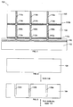
- the wafers are processed in a horizontal orientation for the copper deposition.
- Anodes in the deposition bath also kept horizontal, are disposed directly opposite the wafers. Since dimensionally stable insoluble electrodes are employed, the distance between the anodes and the cathodic parts of the wafer or semiconductor device is maintained substantially constant.
- the process according to the invention is especially suitable for filling vias to form TSVs in silicon substrates in, e.g., semiconductor devices, silicon wafers and MEMS devices.
- a dielectric layer is formed on the inner surface of the vias, during or subsequent to the step of etching to form the initial vias.
- the oxidation of silicon results in the formation of silicon dioxide, and this dielectric material may be employed to provide electrical isolation of the TSVs from the surrounding silicon substrate, chip or wafer.
- the dielectric layer may be formed by any suitable process.
- a silicon dioxide layer is formed, for example, by a TEOS process or by an oxidation of the silicon sidewalls of the via. Suitable methods for formation of a layer of such dielectric materials are known in the art and may be selected by the person of skill in the art as needed.
- a barrier layer is formed on the inner sidewalls of the TSV, in order to provide a barrier to diffusion of the later-deposited copper into the silicon of the substrate through which the TSV is formed.
- the barrier layer is a tantalum-containing material capable of reducing and/or eliminating diffusion of copper therethrough.
- a nitride layer (tantalum nitride layer for example) is formed, for example, by a sputtering process. Suitable methods for formation of a layer of such barrier materials are known in the art and may be selected by the person of skill in the art as needed.
- the barrier layer may be made electrically conductive by deposition of a suitable base metal layer over the barrier layer.
- the base metal layer is subsequently applied, which forms an electrically conductive base for the subsequent electrolytic metallization.
- the base metal layer is applied by a physical metal deposition process and/or by a CVD process and/or by a PECVD process.
- a plating process may also be used, for example an electroless metal deposition process.
- a basic metal layer formed from copper may be deposited.
- Other conductive layers, usually metal layers, may also be suitable.
- Such conductive layers may include, for example, a metal such as tungsten, silver, gold, platinum, zinc, tin or any other metal or silicide known for use as a seed layer for electrodeposition of copper onto a non-conductive substrate.
- the copper fill for the TSV is electrolytically deposited according to the above-described process.
- the process of the present invention is integrated into a semiconductor fabrication process, and includes lithography and masking for the etch process, DRIE or laser etching for creation of the TSV, formation of a dielectric isolation layer by an oxidation, formation of a barrier layer by physical vapor deposition, thermal and/or CVD, formation of a base metal or seed layer by an appropriate method, such as a copper electroless process, copper electrodeposition filling of the TSV as described in detail herein, appropriate treatment such as CMP and cleaning, to complete formation of the filled TSV.
- lithography and masking for the etch process DRIE or laser etching for creation of the TSV
- formation of a dielectric isolation layer by an oxidation formation of a barrier layer by physical vapor deposition, thermal and/or CVD
- formation of a base metal or seed layer by an appropriate method, such as a copper electroless process, copper electrodeposition filling of the TSV as described in detail herein, appropriate treatment such as CMP and cleaning, to complete formation of the filled TSV.
- the wafer or semiconductor device may then be processed using standard technology, such as CMOS, and later subjected to processes such as thinning, lithography, solder bump, dicing and then die-to-die, die-to-wafer, wafer-to-wafer or other appropriate 3D construction by various known methods.
- CMOS complementary metal-oxide-semiconductor
- manufacturing aspects relating to TSVs may include via formation, metallization, wafer thinning, alignment, and bonding.
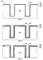
- a wafer is provided with vias having a diameter of about 10 microns and a depth of about 50 microns.
- the vias are initially coated with a dielectric layer of silicon dioxide formed by high temperature oxidation of the inner sidewalls of the vias.
- the dielectric layer on the inner sidewalls of the vias is next coated with a diffusion barrier layer formed from tantalum nitride applied by sputtering.
- the diffusion barrier layer is coated with a copper base metal layer by a sputtering process, in which the copper base metal layer has a thickness of about 0.1 micron.
- the wafer is then immersed in a copper deposition bath described below in which the wafer is connected as a cathode and an insoluble anode is included.
- the via is filled with high purity copper by electrodeposition from the bath having the following ingredients, to form the TSVs in accordance with the present invention: H 2 SO 4 , 98% by wt. 130 g/l CuSO 4 ⁇ 5 H 2 O 70 g/l FeSO 4 ⁇ 7 H 2 O 15 g/l and polyethylene glycol 8 g/l in water.
- the high purity copper is electrodeposited under the following conditions:
- the internal stress is measured as deposited without a post-annealing step.
- the measurement is via wafer warpage and bow (LASER measurement).
- the equipment used was a KLA-TENCOR FLX-2320 thin film stress measurement system, copper film thickness 1 micron, wafer thickness 750 micron.
- FIG. 1 is a schematic cross-sectional view of a 3D device 100 including a substrate 102 having mounted thereon two wafers 104 and 106, including copper-filled TSVs 108a, 108b, 108c, 110a, 110b and 110c, in which the TSVs have been electrodeposited by a process according to an embodiment of the present invention.
- the substrate 102 may be any suitable substrate, such as a chip, a wafer or some other substrate upon which one or more chips or wafers is to be attached to form a 3D device such as the 3D device 100 depicted in FIG. 1 . As shown in FIG.
- the 3D device 100 further includes solder bumps 112a, 112b, 112c, 114a, 114b and 114c, by which the respective filled TSVs 108a, 108b, 108c, 110a, 110b and 110c are electrically interconnected to each other and to electrical wiring 116 in the substrate 102.
- the 3D device 100 further includes under fill material 118 between the wafer 104 and the substrate 102 and between the wafer 104 and the wafer 106. It is noted that FIG.
- FIG. 1 is a highly schematic depiction of a 3D device, and for the sake of clarity and simple explanation omits the various functional elements that would be present in the various elements of the 3D device, so as to more clearly depict the important elements of the 3D device which can be formed by a process including various embodiments of the present invention.
- FIGS. 2-9 are schematic cross-sectional views of steps in a process of forming TSVs in a wafer and mounting the wafer onto a substrate to form part of a 3D device such as the 3D device 100 shown in FIG. 1 , in accordance with an embodiment of the present invention.
- the process depicted in FIGS. 2-9 is presented schematically and, as will be understood, may be carried out in the appropriate selected order as described above, with respect to the "via first" or “via last", before or after FEOL and before or after bonding.
- FIG. 2 depicts a silicon substrate, such as a wafer, chip or other silicon substrate which may be used, e.g., in a semiconductor device, through which TSVs are to be formed.
- a silicon substrate such as a wafer, chip or other silicon substrate which may be used, e.g., in a semiconductor device, through which TSVs are to be formed.
- TSVs are formed in the silicon substrate 104.
- any suitable method of forming TSVs may be used, and in one embodiment, the method is DRIE. This formation is indicated by the arrow leading from FIG. 2 to FIG. 3 .
- FIG. 3 depicts the silicon substrate of FIG. 2 after the TSVs 120a, 120b and 120c have been formed through most of the thickness of the silicon substrate 104. It is noted that, for simplicity, only three TSVs 120a-120c are depicted in FIGS. 1-8 , but as disclosed above, a given wafer or semiconductor device may contain hundreds or thousands of such TSVs. It is further noted that, for simplicity, the TSVs 120a-120c in FIG. 3 , and in all of the FIGS. 1 and 3 -9, are shown as having vertical, parallel sidewalls; this is for purposes of ease of illustration and is not intended to depict a required situation.
- the sidewalls in TSVs generally taper slightly from top to bottom, i.e., from the opening of the via to the bottom of the via, so that the diameter at the bottom is slightly smaller than the diameter at the top opening or mouth of the via.
- each TSV 120a-120c on the entire inside surface of the sidewalls of each TSV 120 there optionally may be deposited a dielectric layer 122, as shown in FIGS. 4 and 4a . Due to the scale of FIG. 4 , an expanded view of a portion of the TSV 120c and the subsequently applied layers are shown in FIGS. 4a, 4b and 4c . As described above, the dielectric layer 122 is provided as an electrical insulation layer between the subsequently formed conductive fill of the TSV and the adjacent silicon substrate 104. The entire inner surface of each TSV 120a-120c should be covered with the dielectric layer 122.
- the relative proportions of the layers and the substrate 104 are not to scale.
- the dielectric layer is optional, and in an appropriate embodiment, the step illustrated in FIG. 4a can be omitted, e.g., when the barrier layer subsequently formed also functions as a dielectric.
- a barrier layer 124 is deposited or formed over the dielectric layer 122, as shown in FIG. 4b .
- the barrier layer may be formed of a material such as, for example, tantalum (Ta), tantalum/tungsten (TaW) or tantalum nitride (TaN), or other material known to function as a barrier to copper migration.
- the barrier layer 124 is provided in order to prevent migration of copper into the adjacent silicon substrate 104.
- the barrier layer may be deposited by any appropriate method known in the art for deposition of such a layer.
- a conductive base metal or seed layer 126 is deposited on the surface of the barrier layer 124 lining the TSVs 120a-120c.
- the base metal layer 126 may be any appropriate conductive metal layer, and in one embodiment is copper, and in another embodiment is high-purity copper.
- the base metal layer 126 may be deposited by any appropriate method known in the art for deposition of such a layer.
- the base metal layer 126 provides a conductive surface upon which the electrodeposition of the TSV fill metal can take place.
- each of the TSVs 120a-120c are filled with high purity copper by an electrodeposition process as described above, to form the filled TSVs 108a-108c, as depicted in FIG. 5 .
- the high purity copper is electrodeposited using the redox system described above, such that the copper is deposited on the base metal layer 126, and the high purity copper completely fills the TSVs with essentially no voids or inclusions, in accordance with an embodiment of the present invention.
- FIGS. 1 and 5 -9 although the dielectric layer 122, the barrier layer 124 and the conductive layer 126 are not clearly shown due to the scale of the drawings, they are deemed to be present, having been formed as described above, and shown in FIGS. 4a, 4b and 4c .
- FIGS. 6-9 schematically depict certain steps in a process of attaching a silicon substrate 104 containing the filled TSVs 108a-108c to the substrate 102. Also, at this time, any needed removal of the variously deposited layers from other surfaces of the wafer may be carried out.
- the copper electrodeposition may cover the entire upper surface of the wafer, and may be removed, e.g., by chemical-mechanical polishing (CMP). Suitable methods for removing excess material deposited in the course of carrying out the processes described herein may be selected as needed by those of skill in the art. These layers and steps for removing them are not shown in the drawings, but will be readily understood and appreciated by the skilled person.
- the wafer containing the newly formed TSVs 108a-108c has been thinned, thus exposing the lower or bottom end of the TSVs 108a-108c to enable electrical connection of the TSVs 108a-108c in subsequent steps.
- the thinning may be carried out by any known method for thinning semiconductor wafers, chips, etc.
- the silicon substrate 104 containing the filled TSVs 108a-108c is positioned above or adjacent to the substrate 102.
- the substrate 102 includes the electrical wiring 116, similar to that shown in FIG. 1 .
- solder beads or balls 112a, 112b and 112c have been placed in locations at which the TSVs 108a-108c will contact exposed portions of the electrical wiring 116.
- the solder beads 112a-112c may be formed of any suitable material, such as tin-lead solder or any other known solder material used for making such attachments, and may be deposited according to any known method.
- the next step is contacting each of the TSVs 108a-108c to the solder beads 112a-112c, which are in turn in contact with the electrical wiring 116 in the substrate 102, and thereby to create an electrical connection between the respective TSVs 108a-108c to the electrical wiring 116 via the respective solder beads 112a-112c.
- the contacting may be by any known method.
- the underfill material 118a can be added to fill the or any space remaining between the silicon substrate 104 and the substrate 102.
- the underfill material is placed following the step of contacting the TSVs to the solder beads, and in another embodiment, the underfill material 118a is applied to the substrate prior to the contacting. As will be understood, the underfill material 118a may be applied before or after the solder beads.
- the step of etching may form TSVs that penetrate through the entire thickness of the silicon substrate (not shown).
- a lower layer to which the wafer has already been bonded may act as an etch stop layer.
- the high conductivity of the copper may be sufficient to provide the electrical conductivity required of the TSVs.
- FIGS. 10-12 are schematic cross-sectional views of steps in a process of forming TSVs in a wafer and mounting the wafer onto a substrate to form part of a 3D device in accordance with another embodiment of the present invention.
- FIG. 10 depicts the wafer into which a TSV is being formed at a point in the process corresponding to FIG. 4c , after the via 220 has been formed, a dielectric layer 222, a barrier layer 224 and a base metal conductive layer 226 have been deposited on the sidewalls in sequence as described with the embodiment of FIGS. 4, 4a, 4b and 4c , and in which the materials deposited and methods therefore are the same as have been described above.
- each of the vias 220 are lined, but are not completely filled, with a relatively thick and uniform layer of highly pure copper by an electrodeposition process as described above, to form the lined TSVs 208, as depicted in FIG. 11 .
- the highly pure copper is electrodeposited using the redox system described above, such that the copper is deposited on the base metal layer 226, and the highly pure copper completely lines the inner walls of the TSVs with a thick layer of the highly pure copper.
- the layer of high purity copper itself contains essentially no voids or inclusions, in accordance with an embodiment of the present invention.
- the layer has a thickness which, when coupled with the relatively large size of the TSV, provides adequate conductivity without requiring the TSV 208 to be completely filled.
- the TSV 208 includes one large, central opening 228, in that the via 220 has not been completely filled but instead is covered with a uniformly thick layer of the high purity copper by the process in accordance with this embodiment of the invention.
- the wafer 200 is then thinned to provide the wafer at the stage shown in FIG. 12 .
- the wafer containing the newly formed TSVs 208 has been thinned, thus exposing the lower or bottom end of the TSVs 208 to enable electrical connection of the TSVs 208 in subsequent steps.
- the thinning may be carried out by any known method for thinning semiconductor wafers, chips, etc.
- the layers including the dielectric layer 222, the barrier layer 224, the base metal layer 226 and the high purity copper layer 208 have not yet been removed from the upper surface of the wafer 200. These layers would also be present in the embodiment of the invention described with respect to FIGS. 2-9 , but in describing that embodiment, the step of removing these layers was not specifically described. Such step would have been carried out subsequent to the step of electroplating with high purity copper in accordance with the invention, and had already been completed at the point in the process depicted in FIG. 5 . In that embodiment, and in the embodiment described with respect to FIG.
- the copper layer can simply be removed, e.g., by CMP, or it can be patterned to create an electrical circuit on that surface of the wafer.
- the pattern may be formed by a photoresist process prior to the step of electroplating with high purity copper. While it is also possible to carry out the pattern formation steps subsequent to the step of electroplating with high purity copper, it is considered to be more efficient to form the pattern, e.g., by a photoresist process, prior to the step of electroplating with high purity copper.
Landscapes
- Chemical & Material Sciences (AREA)
- Engineering & Computer Science (AREA)
- Chemical Kinetics & Catalysis (AREA)
- Electrochemistry (AREA)
- Materials Engineering (AREA)
- Metallurgy (AREA)
- Organic Chemistry (AREA)
- Physics & Mathematics (AREA)
- Condensed Matter Physics & Semiconductors (AREA)
- General Physics & Mathematics (AREA)
- Manufacturing & Machinery (AREA)
- Computer Hardware Design (AREA)
- Microelectronics & Electronic Packaging (AREA)
- Power Engineering (AREA)
- Crystallography & Structural Chemistry (AREA)
- Internal Circuitry In Semiconductor Integrated Circuit Devices (AREA)
- Electroplating Methods And Accessories (AREA)
- Electrodes Of Semiconductors (AREA)
- Electroplating And Plating Baths Therefor (AREA)
Applications Claiming Priority (2)
| Application Number | Priority Date | Filing Date | Title |
|---|---|---|---|
| US12/372,113 US20100206737A1 (en) | 2009-02-17 | 2009-02-17 | Process for electrodeposition of copper chip to chip, chip to wafer and wafer to wafer interconnects in through-silicon vias (tsv) |
| PCT/IB2009/007793 WO2010094998A1 (en) | 2009-02-17 | 2009-12-16 | Process for electrodeposition of copper chip to chip, chip to wafer and wafer to wafer interconnects in through-silicon vias (tsv) |
Publications (2)
| Publication Number | Publication Date |
|---|---|
| EP2399281A1 EP2399281A1 (en) | 2011-12-28 |
| EP2399281B1 true EP2399281B1 (en) | 2016-04-20 |
Family
ID=42126356
Family Applications (1)
| Application Number | Title | Priority Date | Filing Date |
|---|---|---|---|
| EP09799392.7A Not-in-force EP2399281B1 (en) | 2009-02-17 | 2009-12-16 | Process for electrodeposition of copper chip to chip, chip to wafer and wafer to wafer interconnects in through-silicon vias (tsv) |
Country Status (6)
| Country | Link |
|---|---|
| US (1) | US20100206737A1 (ja) |
| EP (1) | EP2399281B1 (ja) |
| JP (1) | JP5743907B2 (ja) |
| CN (1) | CN102318041B (ja) |
| TW (1) | TW201034120A (ja) |
| WO (1) | WO2010094998A1 (ja) |
Families Citing this family (62)
| Publication number | Priority date | Publication date | Assignee | Title |
|---|---|---|---|---|
| US7816181B1 (en) * | 2009-06-30 | 2010-10-19 | Sandisk Corporation | Method of under-filling semiconductor die in a die stack and semiconductor device formed thereby |
| US9714474B2 (en) * | 2010-04-06 | 2017-07-25 | Tel Nexx, Inc. | Seed layer deposition in microscale features |
| US20120024713A1 (en) * | 2010-07-29 | 2012-02-02 | Preisser Robert F | Process for electrodeposition of copper chip to chip, chip to wafer and wafer to wafer interconnects in through-silicon vias (tsv) with heated substrate and cooled electrolyte |
| US20120056331A1 (en) * | 2010-09-06 | 2012-03-08 | Electronics And Telecommunications Research Institute | Methods of forming semiconductor device and semiconductor devices formed by the same |
| US8786066B2 (en) * | 2010-09-24 | 2014-07-22 | Intel Corporation | Die-stacking using through-silicon vias on bumpless build-up layer substrates including embedded-dice, and processes of forming same |
| JP5981455B2 (ja) * | 2011-01-26 | 2016-08-31 | エンソン インコーポレイテッド | マイクロ電子工業におけるビアホール充填方法 |
| US8970043B2 (en) | 2011-02-01 | 2015-03-03 | Maxim Integrated Products, Inc. | Bonded stacked wafers and methods of electroplating bonded stacked wafers |
| JP5754209B2 (ja) * | 2011-03-31 | 2015-07-29 | 大日本印刷株式会社 | 半導体装置の製造方法 |
| US8753981B2 (en) | 2011-04-22 | 2014-06-17 | Micron Technology, Inc. | Microelectronic devices with through-silicon vias and associated methods of manufacturing |
| EP2518187A1 (en) * | 2011-04-26 | 2012-10-31 | Atotech Deutschland GmbH | Aqueous acidic bath for electrolytic deposition of copper |
| US8691691B2 (en) | 2011-07-29 | 2014-04-08 | International Business Machines Corporation | TSV pillar as an interconnecting structure |
| US8894868B2 (en) | 2011-10-06 | 2014-11-25 | Electro Scientific Industries, Inc. | Substrate containing aperture and methods of forming the same |
| CN102376641B (zh) * | 2011-11-24 | 2013-07-10 | 上海华力微电子有限公司 | 铜填充硅通孔的制作方法 |
| US20130140688A1 (en) * | 2011-12-02 | 2013-06-06 | Chun-Hung Chen | Through Silicon Via and Method of Manufacturing the Same |
| CN102569251B (zh) * | 2012-02-22 | 2014-07-02 | 华进半导体封装先导技术研发中心有限公司 | 三维封装用金属间化合物填充的垂直通孔互连结构及制备方法 |
| US20130249047A1 (en) * | 2012-03-26 | 2013-09-26 | Nanya Technology Corporation | Through silicon via structure and method for fabricating the same |
| CN103378057B (zh) * | 2012-04-20 | 2016-06-29 | 南亚科技股份有限公司 | 半导体芯片以及其形成方法 |
| CN103378059B (zh) * | 2012-04-27 | 2016-04-27 | 南亚科技股份有限公司 | 穿硅通孔与其形成方法 |
| US9006896B2 (en) * | 2012-05-07 | 2015-04-14 | Xintec Inc. | Chip package and method for forming the same |
| CN104396009A (zh) * | 2012-06-07 | 2015-03-04 | 伦塞勒工艺研究所 | 用以减少三维集成中硅穿孔(tsv)压力的保角涂层弹性垫的使用 |
| CN102703938B (zh) * | 2012-06-07 | 2015-04-22 | 上海交通大学 | 硫酸铜电镀液的应力消除剂 |
| WO2014012381A1 (zh) * | 2012-07-17 | 2014-01-23 | 上海交通大学 | 铜互连微柱力学性能原位压缩试样及其制备方法 |
| CN103715132B (zh) * | 2012-09-29 | 2017-12-01 | 中芯国际集成电路制造(上海)有限公司 | 金属互连结构的形成方法 |
| US8933564B2 (en) * | 2012-12-21 | 2015-01-13 | Intel Corporation | Landing structure for through-silicon via |
| CN103060859B (zh) * | 2012-12-27 | 2015-04-22 | 建滔(连州)铜箔有限公司 | 用于改善毛箔毛面锋形的添加剂和电解铜箔生产工艺 |
| CN103103585B (zh) * | 2012-12-29 | 2015-09-16 | 上海新阳半导体材料股份有限公司 | 一种用于铜互连的高速凸点电镀方法 |
| JP6142880B2 (ja) * | 2013-01-15 | 2017-06-07 | 三菱瓦斯化学株式会社 | シリコンエッチング液およびエッチング方法並びに微小電気機械素子 |
| EP2754732B1 (en) * | 2013-01-15 | 2015-03-11 | ATOTECH Deutschland GmbH | Aqueous composition for etching of copper and copper alloys |
| KR20140094061A (ko) * | 2013-01-16 | 2014-07-30 | 주식회사 잉크테크 | 연속 도금 장치 및 연속 도금 방법 |
| US8933562B2 (en) | 2013-01-24 | 2015-01-13 | International Business Machines Corporation | In-situ thermoelectric cooling |
| US9470710B2 (en) | 2013-02-27 | 2016-10-18 | Texas Instruments Incorporated | Capacitive MEMS sensor devices |
| CN103280427B (zh) * | 2013-06-13 | 2016-08-10 | 华进半导体封装先导技术研发中心有限公司 | 一种tsv正面端部互连工艺 |
| CN103290438B (zh) * | 2013-06-25 | 2015-12-02 | 深圳市创智成功科技有限公司 | 用于晶圆级封装的电镀铜溶液及电镀方法 |
| KR101750795B1 (ko) * | 2013-06-27 | 2017-06-26 | 인텔 아이피 코포레이션 | 전자 시스템을 위한 고 전도성 고 주파수 비아 |
| CN103361681B (zh) * | 2013-08-08 | 2016-11-16 | 上海新阳半导体材料股份有限公司 | 能改变tsv微孔镀铜填充方式的添加剂c及包含其的电镀液 |
| US20150069609A1 (en) * | 2013-09-12 | 2015-03-12 | International Business Machines Corporation | 3d chip crackstop |
| KR20150057148A (ko) * | 2013-11-18 | 2015-05-28 | 삼성전자주식회사 | 반도체 장치 |
| CN103695973B (zh) * | 2013-12-17 | 2016-07-06 | 上海交通大学 | 在铜互连甲基磺酸铜镀液中添加Fe2+和Fe3+的电镀方法 |
| CN103668356B (zh) * | 2013-12-17 | 2016-04-13 | 上海交通大学 | 在铜互连硫酸铜镀液中添加Fe2+和Fe3+的电镀方法 |
| US9373613B2 (en) * | 2013-12-31 | 2016-06-21 | Skyworks Solutions, Inc. | Amplifier voltage limiting using punch-through effect |
| CN104465564B (zh) * | 2014-01-06 | 2017-09-15 | 昆山西钛微电子科技有限公司 | 晶圆级芯片tsv封装结构及其封装方法 |
| CN103887232B (zh) * | 2014-04-04 | 2016-08-24 | 华进半导体封装先导技术研发中心有限公司 | 改善tsv金属填充均匀性的方法 |
| US9515035B2 (en) | 2014-12-19 | 2016-12-06 | International Business Machines Corporation | Three-dimensional integrated circuit integration |
| US9971970B1 (en) * | 2015-04-27 | 2018-05-15 | Rigetti & Co, Inc. | Microwave integrated quantum circuits with VIAS and methods for making the same |
| US20170145577A1 (en) * | 2015-11-19 | 2017-05-25 | Rohm And Haas Electronic Materials Llc | Method of electroplating low internal stress copper deposits on thin film substrates to inhibit warping |
| FR3046878B1 (fr) * | 2016-01-19 | 2018-05-18 | Kobus Sas | Procede de fabrication d'une interconnexion comprenant un via s'etendant au travers d'un substrat |
| CN107706146B (zh) * | 2016-08-08 | 2020-07-28 | 中芯国际集成电路制造(上海)有限公司 | 半导体器件的制备方法 |
| CN106757191B (zh) * | 2016-11-23 | 2019-10-01 | 苏州昕皓新材料科技有限公司 | 一种具有高择优取向的铜晶体颗粒及其制备方法 |
| US11121301B1 (en) | 2017-06-19 | 2021-09-14 | Rigetti & Co, Inc. | Microwave integrated quantum circuits with cap wafers and their methods of manufacture |
| US10475808B2 (en) | 2017-08-30 | 2019-11-12 | Macronix International Co., Ltd. | Three dimensional memory device and method for fabricating the same |
| CN108615704B (zh) * | 2018-03-27 | 2020-05-08 | 中国科学院上海微系统与信息技术研究所 | 一种硅通孔互连的制作工艺、由此形成的硅通孔互连结构及其应用 |
| CN108754555B (zh) * | 2018-08-29 | 2020-04-28 | 广东天承科技有限公司 | 一种电镀液及其电镀方法 |
| US10867855B2 (en) | 2019-05-13 | 2020-12-15 | Honeywell International Inc. | Through silicon via fabrication |
| TW202118365A (zh) | 2019-08-19 | 2021-05-01 | 德商德國艾托特克公司 | 高密度互連印刷電路板的製造順序及高密度互連印刷電路板 |
| KR20220047360A (ko) | 2019-08-19 | 2022-04-15 | 아토테크 도이칠란트 게엠베하 운트 콤파니 카게 | 구리로 충전된 마이크로비아들을 포함하는 고밀도 상호연결 인쇄 회로 기판을 제조하는 방법 |
| CN110453255B (zh) * | 2019-08-30 | 2020-10-09 | 广州皓悦新材料科技有限公司 | 一种具有高深镀能力的vcp镀铜光亮剂及其制备方法 |
| CN111041535A (zh) * | 2019-12-25 | 2020-04-21 | 浙江振有电子股份有限公司 | 一种连续移动式电镀通孔双面板的方法 |
| CN111155152B (zh) * | 2019-12-26 | 2022-11-01 | 西安泰金工业电化学技术有限公司 | 一种用于pcb水平电镀工序中降低生产成本的方法 |
| TWI741466B (zh) | 2019-12-27 | 2021-10-01 | 鉑識科技股份有限公司 | 利用水/醇溶性有機添加劑製備之奈米雙晶層及其製備方法 |
| CN112018078B (zh) * | 2020-07-29 | 2022-10-25 | 复旦大学 | 一种铜互连结构及其制作方法 |
| CN112151504B (zh) * | 2020-08-17 | 2022-04-29 | 复旦大学 | 一种带有封孔层的铜互连结构及其制备方法 |
| CN113174620B (zh) * | 2021-04-22 | 2022-05-03 | 浙江集迈科微电子有限公司 | 一种镀液流速加强型tsv金属柱的电镀方法 |
Family Cites Families (19)
| Publication number | Priority date | Publication date | Assignee | Title |
|---|---|---|---|---|
| DE4344387C2 (de) * | 1993-12-24 | 1996-09-05 | Atotech Deutschland Gmbh | Verfahren zur elektrolytischen Abscheidung von Kupfer und Anordnung zur Durchführung des Verfahrens |
| DE19545231A1 (de) * | 1995-11-21 | 1997-05-22 | Atotech Deutschland Gmbh | Verfahren zur elektrolytischen Abscheidung von Metallschichten |
| DE19653681C2 (de) * | 1996-12-13 | 2000-04-06 | Atotech Deutschland Gmbh | Verfahren zur elektrolytischen Abscheidung von Kupferschichten mit gleichmäßiger Schichtdicke und guten optischen und metallphysikalischen Eigenschaften und Anwendung des Verfahrens |
| ATE282248T1 (de) * | 1999-01-21 | 2004-11-15 | Atotech Deutschland Gmbh | Verfahren zum galvanischen bilden von leiterstrukturen aus hochreinem kupfer bei der herstellung von integrierten schaltungen |
| US20040045832A1 (en) * | 1999-10-14 | 2004-03-11 | Nicholas Martyak | Electrolytic copper plating solutions |
| JP2001267726A (ja) * | 2000-03-22 | 2001-09-28 | Toyota Autom Loom Works Ltd | 配線基板の電解メッキ方法及び配線基板の電解メッキ装置 |
| JP2004119606A (ja) * | 2002-09-25 | 2004-04-15 | Canon Inc | 半導体基板の貫通孔埋め込み方法および半導体基板 |
| DE10311575B4 (de) * | 2003-03-10 | 2007-03-22 | Atotech Deutschland Gmbh | Verfahren zum elektrolytischen Metallisieren von Werkstücken mit Bohrungen mit einem hohen Aspektverhältnis |
| US20090008792A1 (en) * | 2004-11-19 | 2009-01-08 | Industrial Technology Research Institute | Three-dimensional chip-stack package and active component on a substrate |
| JP4456027B2 (ja) * | 2005-03-25 | 2010-04-28 | Okiセミコンダクタ株式会社 | 貫通導電体の製造方法 |
| ATE484943T1 (de) * | 2006-03-30 | 2010-10-15 | Atotech Deutschland Gmbh | Elektrolytisches verfahren zum füllen von löchern und vertiefungen mit metallen |
| KR100945504B1 (ko) * | 2007-06-26 | 2010-03-09 | 주식회사 하이닉스반도체 | 스택 패키지 및 그의 제조 방법 |
| US7939941B2 (en) * | 2007-06-27 | 2011-05-10 | Taiwan Semiconductor Manufacturing Company, Ltd. | Formation of through via before contact processing |
| US7825517B2 (en) * | 2007-07-16 | 2010-11-02 | Taiwan Semiconductor Manufacturing Company, Ltd. | Method for packaging semiconductor dies having through-silicon vias |
| KR101185886B1 (ko) * | 2007-07-23 | 2012-09-25 | 삼성전자주식회사 | 유니버설 배선 라인들을 포함하는 반도체 칩, 반도체패키지, 카드 및 시스템 |
| TWI335059B (en) * | 2007-07-31 | 2010-12-21 | Siliconware Precision Industries Co Ltd | Multi-chip stack structure having silicon channel and method for fabricating the same |
| TWI341554B (en) * | 2007-08-02 | 2011-05-01 | Enthone | Copper metallization of through silicon via |
| US7902069B2 (en) * | 2007-08-02 | 2011-03-08 | International Business Machines Corporation | Small area, robust silicon via structure and process |
| US7776741B2 (en) * | 2008-08-18 | 2010-08-17 | Novellus Systems, Inc. | Process for through silicon via filing |
-
2009
- 2009-02-17 US US12/372,113 patent/US20100206737A1/en not_active Abandoned
- 2009-12-16 CN CN200980156992.4A patent/CN102318041B/zh not_active Expired - Fee Related
- 2009-12-16 EP EP09799392.7A patent/EP2399281B1/en not_active Not-in-force
- 2009-12-16 JP JP2011549685A patent/JP5743907B2/ja not_active Expired - Fee Related
- 2009-12-16 WO PCT/IB2009/007793 patent/WO2010094998A1/en active Application Filing
- 2009-12-22 TW TW098144125A patent/TW201034120A/zh unknown
Also Published As
| Publication number | Publication date |
|---|---|
| CN102318041B (zh) | 2014-05-07 |
| WO2010094998A1 (en) | 2010-08-26 |
| US20100206737A1 (en) | 2010-08-19 |
| EP2399281A1 (en) | 2011-12-28 |
| TW201034120A (en) | 2010-09-16 |
| JP2012518084A (ja) | 2012-08-09 |
| JP5743907B2 (ja) | 2015-07-01 |
| CN102318041A (zh) | 2012-01-11 |
Similar Documents
| Publication | Publication Date | Title |
|---|---|---|
| EP2399281B1 (en) | Process for electrodeposition of copper chip to chip, chip to wafer and wafer to wafer interconnects in through-silicon vias (tsv) | |
| EP2611950B1 (en) | Process for electrodeposition of copper chip to chip chip to wafer and wafer to wafer interconnects in through-silicon vias (tsv), with heated substrate and cooled electrolyte | |
| CN105845558B (zh) | 穿硅通孔填充工艺 | |
| KR100420157B1 (ko) | 작업편 상에 전해하여 금속을 증착시키는 장치 및 방법 | |
| JP2009527912A (ja) | 半導体デバイスの製造において直接銅めっきし、かつ充填して相互配線を形成するための方法及び組成物 | |
| US20230212773A1 (en) | Surface pretreatment for electroplating nanotwinned copper | |
| WO2020123322A2 (en) | Low temperature direct copper-copper bonding | |
| KR20130108978A (ko) | 구리 도금 조성물 및 이 조성물을 사용한 반도체 기판에서 공동을 충진하기 위한 공정 | |
| TW575948B (en) | Tungsten encapsulated copper interconnections using electroplating | |
| US20130249096A1 (en) | Through silicon via filling | |
| JP2013524019A (ja) | ミクロスケール構造中でのシード層堆積 | |
| US8970027B2 (en) | Metallization mixtures and electronic devices | |
| KR101752945B1 (ko) | 구리 및 구리 합금의 에칭 방법 | |
| US20130213816A1 (en) | Incorporating High-Purity Copper Deposit As Smoothing Step After Direct On-Barrier Plating To Improve Quality Of Deposited Nucleation Metal In Microscale Features | |
| WO2011018478A1 (en) | Electrolyte and method for the electroplating of copper on a barrier layer, and semiconductor substrate obtained with said method | |
| JP4472673B2 (ja) | 銅配線の製造方法及び銅めっき用電解液 | |
| US7597787B2 (en) | Methods and apparatuses for electrochemical deposition | |
| US20020079232A1 (en) | Seed layer deposition |
Legal Events
| Date | Code | Title | Description |
|---|---|---|---|
| PUAI | Public reference made under article 153(3) epc to a published international application that has entered the european phase |
Free format text: ORIGINAL CODE: 0009012 |
|
| 17P | Request for examination filed |
Effective date: 20110919 |
|
| AK | Designated contracting states |
Kind code of ref document: A1 Designated state(s): AT BE BG CH CY CZ DE DK EE ES FI FR GB GR HR HU IE IS IT LI LT LU LV MC MK MT NL NO PL PT RO SE SI SK SM TR |
|
| DAX | Request for extension of the european patent (deleted) | ||
| RAP1 | Party data changed (applicant data changed or rights of an application transferred) |
Owner name: ATOTECH DEUTSCHLAND GMBH |
|
| GRAP | Despatch of communication of intention to grant a patent |
Free format text: ORIGINAL CODE: EPIDOSNIGR1 |
|
| RIC1 | Information provided on ipc code assigned before grant |
Ipc: C25D 3/38 20060101ALI20151127BHEP Ipc: C25D 5/18 20060101ALI20151127BHEP Ipc: H01L 21/288 20060101AFI20151127BHEP Ipc: C25D 5/02 20060101ALI20151127BHEP Ipc: C25D 7/12 20060101ALI20151127BHEP Ipc: H01L 21/768 20060101ALI20151127BHEP Ipc: C25D 21/16 20060101ALI20151127BHEP |
|
| INTG | Intention to grant announced |
Effective date: 20151216 |
|
| GRAS | Grant fee paid |
Free format text: ORIGINAL CODE: EPIDOSNIGR3 |
|
| GRAA | (expected) grant |
Free format text: ORIGINAL CODE: 0009210 |
|
| AK | Designated contracting states |
Kind code of ref document: B1 Designated state(s): AT BE BG CH CY CZ DE DK EE ES FI FR GB GR HR HU IE IS IT LI LT LU LV MC MK MT NL NO PL PT RO SE SI SK SM TR |
|
| REG | Reference to a national code |
Ref country code: GB Ref legal event code: FG4D |
|
| REG | Reference to a national code |
Ref country code: CH Ref legal event code: EP |
|
| REG | Reference to a national code |
Ref country code: AT Ref legal event code: REF Ref document number: 793260 Country of ref document: AT Kind code of ref document: T Effective date: 20160515 |
|
| REG | Reference to a national code |
Ref country code: IE Ref legal event code: FG4D |
|
| REG | Reference to a national code |
Ref country code: DE Ref legal event code: R096 Ref document number: 602009038053 Country of ref document: DE |
|
| REG | Reference to a national code |
Ref country code: LT Ref legal event code: MG4D |
|
| REG | Reference to a national code |
Ref country code: AT Ref legal event code: MK05 Ref document number: 793260 Country of ref document: AT Kind code of ref document: T Effective date: 20160420 |
|
| REG | Reference to a national code |
Ref country code: NL Ref legal event code: MP Effective date: 20160420 |
|
| PG25 | Lapsed in a contracting state [announced via postgrant information from national office to epo] |
Ref country code: NL Free format text: LAPSE BECAUSE OF FAILURE TO SUBMIT A TRANSLATION OF THE DESCRIPTION OR TO PAY THE FEE WITHIN THE PRESCRIBED TIME-LIMIT Effective date: 20160420 Ref country code: PL Free format text: LAPSE BECAUSE OF FAILURE TO SUBMIT A TRANSLATION OF THE DESCRIPTION OR TO PAY THE FEE WITHIN THE PRESCRIBED TIME-LIMIT Effective date: 20160420 Ref country code: FI Free format text: LAPSE BECAUSE OF FAILURE TO SUBMIT A TRANSLATION OF THE DESCRIPTION OR TO PAY THE FEE WITHIN THE PRESCRIBED TIME-LIMIT Effective date: 20160420 Ref country code: NO Free format text: LAPSE BECAUSE OF FAILURE TO SUBMIT A TRANSLATION OF THE DESCRIPTION OR TO PAY THE FEE WITHIN THE PRESCRIBED TIME-LIMIT Effective date: 20160720 Ref country code: LT Free format text: LAPSE BECAUSE OF FAILURE TO SUBMIT A TRANSLATION OF THE DESCRIPTION OR TO PAY THE FEE WITHIN THE PRESCRIBED TIME-LIMIT Effective date: 20160420 |
|
| PG25 | Lapsed in a contracting state [announced via postgrant information from national office to epo] |
Ref country code: GR Free format text: LAPSE BECAUSE OF FAILURE TO SUBMIT A TRANSLATION OF THE DESCRIPTION OR TO PAY THE FEE WITHIN THE PRESCRIBED TIME-LIMIT Effective date: 20160721 Ref country code: LV Free format text: LAPSE BECAUSE OF FAILURE TO SUBMIT A TRANSLATION OF THE DESCRIPTION OR TO PAY THE FEE WITHIN THE PRESCRIBED TIME-LIMIT Effective date: 20160420 Ref country code: SE Free format text: LAPSE BECAUSE OF FAILURE TO SUBMIT A TRANSLATION OF THE DESCRIPTION OR TO PAY THE FEE WITHIN THE PRESCRIBED TIME-LIMIT Effective date: 20160420 Ref country code: HR Free format text: LAPSE BECAUSE OF FAILURE TO SUBMIT A TRANSLATION OF THE DESCRIPTION OR TO PAY THE FEE WITHIN THE PRESCRIBED TIME-LIMIT Effective date: 20160420 Ref country code: AT Free format text: LAPSE BECAUSE OF FAILURE TO SUBMIT A TRANSLATION OF THE DESCRIPTION OR TO PAY THE FEE WITHIN THE PRESCRIBED TIME-LIMIT Effective date: 20160420 Ref country code: ES Free format text: LAPSE BECAUSE OF FAILURE TO SUBMIT A TRANSLATION OF THE DESCRIPTION OR TO PAY THE FEE WITHIN THE PRESCRIBED TIME-LIMIT Effective date: 20160420 Ref country code: PT Free format text: LAPSE BECAUSE OF FAILURE TO SUBMIT A TRANSLATION OF THE DESCRIPTION OR TO PAY THE FEE WITHIN THE PRESCRIBED TIME-LIMIT Effective date: 20160822 |
|
| REG | Reference to a national code |
Ref country code: FR Ref legal event code: PLFP Year of fee payment: 8 |
|
| PG25 | Lapsed in a contracting state [announced via postgrant information from national office to epo] |
Ref country code: BE Free format text: LAPSE BECAUSE OF FAILURE TO SUBMIT A TRANSLATION OF THE DESCRIPTION OR TO PAY THE FEE WITHIN THE PRESCRIBED TIME-LIMIT Effective date: 20160420 |
|
| REG | Reference to a national code |
Ref country code: DE Ref legal event code: R097 Ref document number: 602009038053 Country of ref document: DE |
|
| PG25 | Lapsed in a contracting state [announced via postgrant information from national office to epo] |
Ref country code: RO Free format text: LAPSE BECAUSE OF FAILURE TO SUBMIT A TRANSLATION OF THE DESCRIPTION OR TO PAY THE FEE WITHIN THE PRESCRIBED TIME-LIMIT Effective date: 20160420 Ref country code: EE Free format text: LAPSE BECAUSE OF FAILURE TO SUBMIT A TRANSLATION OF THE DESCRIPTION OR TO PAY THE FEE WITHIN THE PRESCRIBED TIME-LIMIT Effective date: 20160420 Ref country code: DK Free format text: LAPSE BECAUSE OF FAILURE TO SUBMIT A TRANSLATION OF THE DESCRIPTION OR TO PAY THE FEE WITHIN THE PRESCRIBED TIME-LIMIT Effective date: 20160420 Ref country code: SK Free format text: LAPSE BECAUSE OF FAILURE TO SUBMIT A TRANSLATION OF THE DESCRIPTION OR TO PAY THE FEE WITHIN THE PRESCRIBED TIME-LIMIT Effective date: 20160420 Ref country code: CZ Free format text: LAPSE BECAUSE OF FAILURE TO SUBMIT A TRANSLATION OF THE DESCRIPTION OR TO PAY THE FEE WITHIN THE PRESCRIBED TIME-LIMIT Effective date: 20160420 |
|
| PLBE | No opposition filed within time limit |
Free format text: ORIGINAL CODE: 0009261 |
|
| STAA | Information on the status of an ep patent application or granted ep patent |
Free format text: STATUS: NO OPPOSITION FILED WITHIN TIME LIMIT |
|
| PG25 | Lapsed in a contracting state [announced via postgrant information from national office to epo] |
Ref country code: SM Free format text: LAPSE BECAUSE OF FAILURE TO SUBMIT A TRANSLATION OF THE DESCRIPTION OR TO PAY THE FEE WITHIN THE PRESCRIBED TIME-LIMIT Effective date: 20160420 |
|
| 26N | No opposition filed |
Effective date: 20170123 |
|
| PG25 | Lapsed in a contracting state [announced via postgrant information from national office to epo] |
Ref country code: SI Free format text: LAPSE BECAUSE OF FAILURE TO SUBMIT A TRANSLATION OF THE DESCRIPTION OR TO PAY THE FEE WITHIN THE PRESCRIBED TIME-LIMIT Effective date: 20160420 |
|
| REG | Reference to a national code |
Ref country code: CH Ref legal event code: PL |
|
| GBPC | Gb: european patent ceased through non-payment of renewal fee |
Effective date: 20161216 |
|
| PG25 | Lapsed in a contracting state [announced via postgrant information from national office to epo] |
Ref country code: MC Free format text: LAPSE BECAUSE OF FAILURE TO SUBMIT A TRANSLATION OF THE DESCRIPTION OR TO PAY THE FEE WITHIN THE PRESCRIBED TIME-LIMIT Effective date: 20160420 |
|
| REG | Reference to a national code |
Ref country code: IE Ref legal event code: MM4A |
|
| PG25 | Lapsed in a contracting state [announced via postgrant information from national office to epo] |
Ref country code: CH Free format text: LAPSE BECAUSE OF NON-PAYMENT OF DUE FEES Effective date: 20161231 Ref country code: LI Free format text: LAPSE BECAUSE OF NON-PAYMENT OF DUE FEES Effective date: 20161231 Ref country code: LU Free format text: LAPSE BECAUSE OF NON-PAYMENT OF DUE FEES Effective date: 20161216 |
|
| PG25 | Lapsed in a contracting state [announced via postgrant information from national office to epo] |
Ref country code: GB Free format text: LAPSE BECAUSE OF NON-PAYMENT OF DUE FEES Effective date: 20161216 Ref country code: IE Free format text: LAPSE BECAUSE OF NON-PAYMENT OF DUE FEES Effective date: 20161216 |
|
| REG | Reference to a national code |
Ref country code: FR Ref legal event code: PLFP Year of fee payment: 9 |
|
| PGFP | Annual fee paid to national office [announced via postgrant information from national office to epo] |
Ref country code: DE Payment date: 20171211 Year of fee payment: 9 Ref country code: FR Payment date: 20171221 Year of fee payment: 9 |
|
| PG25 | Lapsed in a contracting state [announced via postgrant information from national office to epo] |
Ref country code: CY Free format text: LAPSE BECAUSE OF FAILURE TO SUBMIT A TRANSLATION OF THE DESCRIPTION OR TO PAY THE FEE WITHIN THE PRESCRIBED TIME-LIMIT Effective date: 20160420 Ref country code: HU Free format text: LAPSE BECAUSE OF FAILURE TO SUBMIT A TRANSLATION OF THE DESCRIPTION OR TO PAY THE FEE WITHIN THE PRESCRIBED TIME-LIMIT; INVALID AB INITIO Effective date: 20091216 |
|
| PGFP | Annual fee paid to national office [announced via postgrant information from national office to epo] |
Ref country code: IT Payment date: 20171221 Year of fee payment: 9 |
|
| PG25 | Lapsed in a contracting state [announced via postgrant information from national office to epo] |
Ref country code: IS Free format text: LAPSE BECAUSE OF FAILURE TO SUBMIT A TRANSLATION OF THE DESCRIPTION OR TO PAY THE FEE WITHIN THE PRESCRIBED TIME-LIMIT Effective date: 20160420 Ref country code: TR Free format text: LAPSE BECAUSE OF FAILURE TO SUBMIT A TRANSLATION OF THE DESCRIPTION OR TO PAY THE FEE WITHIN THE PRESCRIBED TIME-LIMIT Effective date: 20160420 Ref country code: MK Free format text: LAPSE BECAUSE OF FAILURE TO SUBMIT A TRANSLATION OF THE DESCRIPTION OR TO PAY THE FEE WITHIN THE PRESCRIBED TIME-LIMIT Effective date: 20160420 |
|
| PG25 | Lapsed in a contracting state [announced via postgrant information from national office to epo] |
Ref country code: BG Free format text: LAPSE BECAUSE OF FAILURE TO SUBMIT A TRANSLATION OF THE DESCRIPTION OR TO PAY THE FEE WITHIN THE PRESCRIBED TIME-LIMIT Effective date: 20160420 |
|
| PG25 | Lapsed in a contracting state [announced via postgrant information from national office to epo] |
Ref country code: MT Free format text: LAPSE BECAUSE OF NON-PAYMENT OF DUE FEES Effective date: 20161216 |
|
| REG | Reference to a national code |
Ref country code: DE Ref legal event code: R119 Ref document number: 602009038053 Country of ref document: DE |
|
| PG25 | Lapsed in a contracting state [announced via postgrant information from national office to epo] |
Ref country code: DE Free format text: LAPSE BECAUSE OF NON-PAYMENT OF DUE FEES Effective date: 20190702 Ref country code: FR Free format text: LAPSE BECAUSE OF NON-PAYMENT OF DUE FEES Effective date: 20181231 Ref country code: IT Free format text: LAPSE BECAUSE OF NON-PAYMENT OF DUE FEES Effective date: 20181216 |