EP2264223A2 - Carbure de silicium sans micro-tuyaux et procédé de fabrication correspondant - Google Patents
Carbure de silicium sans micro-tuyaux et procédé de fabrication correspondant Download PDFInfo
- Publication number
- EP2264223A2 EP2264223A2 EP10182708A EP10182708A EP2264223A2 EP 2264223 A2 EP2264223 A2 EP 2264223A2 EP 10182708 A EP10182708 A EP 10182708A EP 10182708 A EP10182708 A EP 10182708A EP 2264223 A2 EP2264223 A2 EP 2264223A2
- Authority
- EP
- European Patent Office
- Prior art keywords
- sic
- micropipe
- seed
- wafer
- free
- Prior art date
- Legal status (The legal status is an assumption and is not a legal conclusion. Google has not performed a legal analysis and makes no representation as to the accuracy of the status listed.)
- Ceased
Links
- 238000000034 method Methods 0.000 title claims abstract description 126
- HBMJWWWQQXIZIP-UHFFFAOYSA-N silicon carbide Chemical compound [Si+]#[C-] HBMJWWWQQXIZIP-UHFFFAOYSA-N 0.000 title claims description 166
- 229910010271 silicon carbide Inorganic materials 0.000 title claims description 164
- 238000004519 manufacturing process Methods 0.000 title description 11
- 239000000463 material Substances 0.000 claims abstract description 174
- 239000013078 crystal Substances 0.000 claims abstract description 93
- 230000008569 process Effects 0.000 claims abstract description 74
- 230000008022 sublimation Effects 0.000 claims abstract description 62
- 238000000859 sublimation Methods 0.000 claims abstract description 62
- 238000006243 chemical reaction Methods 0.000 claims abstract description 60
- 239000004065 semiconductor Substances 0.000 claims abstract description 57
- 239000012535 impurity Substances 0.000 claims abstract description 29
- 230000007547 defect Effects 0.000 claims abstract description 16
- 230000004907 flux Effects 0.000 claims abstract description 15
- 239000000203 mixture Substances 0.000 claims abstract description 14
- 239000000470 constituent Substances 0.000 claims abstract description 12
- 230000001939 inductive effect Effects 0.000 claims abstract description 12
- 239000000758 substrate Substances 0.000 claims description 42
- 239000002019 doping agent Substances 0.000 claims description 18
- 230000004888 barrier function Effects 0.000 claims description 10
- 230000005669 field effect Effects 0.000 claims description 6
- 230000000694 effects Effects 0.000 claims description 3
- 235000012431 wafers Nutrition 0.000 description 57
- 238000005130 seeded sublimation method Methods 0.000 description 16
- 230000015572 biosynthetic process Effects 0.000 description 12
- 230000006911 nucleation Effects 0.000 description 12
- 238000010899 nucleation Methods 0.000 description 12
- 239000007789 gas Substances 0.000 description 8
- 229910052751 metal Inorganic materials 0.000 description 8
- 239000002184 metal Substances 0.000 description 8
- OKTJSMMVPCPJKN-UHFFFAOYSA-N Carbon Chemical compound [C] OKTJSMMVPCPJKN-UHFFFAOYSA-N 0.000 description 7
- 229910052799 carbon Inorganic materials 0.000 description 7
- 238000010438 heat treatment Methods 0.000 description 7
- XEEYBQQBJWHFJM-UHFFFAOYSA-N Iron Chemical compound [Fe] XEEYBQQBJWHFJM-UHFFFAOYSA-N 0.000 description 5
- PXHVJJICTQNCMI-UHFFFAOYSA-N Nickel Chemical compound [Ni] PXHVJJICTQNCMI-UHFFFAOYSA-N 0.000 description 5
- 230000002829 reductive effect Effects 0.000 description 5
- 230000007847 structural defect Effects 0.000 description 5
- 229910052804 chromium Inorganic materials 0.000 description 4
- 239000011651 chromium Substances 0.000 description 4
- 229910052742 iron Inorganic materials 0.000 description 4
- 229910021421 monocrystalline silicon Inorganic materials 0.000 description 4
- 229910052759 nickel Inorganic materials 0.000 description 4
- 238000000926 separation method Methods 0.000 description 4
- 239000007787 solid Substances 0.000 description 4
- 238000002441 X-ray diffraction Methods 0.000 description 3
- 238000013459 approach Methods 0.000 description 3
- 229910052802 copper Inorganic materials 0.000 description 3
- 238000013461 design Methods 0.000 description 3
- 230000008030 elimination Effects 0.000 description 3
- 238000003379 elimination reaction Methods 0.000 description 3
- 230000001747 exhibiting effect Effects 0.000 description 3
- 239000012774 insulation material Substances 0.000 description 3
- 229910052748 manganese Inorganic materials 0.000 description 3
- 239000011572 manganese Substances 0.000 description 3
- 230000007246 mechanism Effects 0.000 description 3
- 229910052750 molybdenum Inorganic materials 0.000 description 3
- 229910052763 palladium Inorganic materials 0.000 description 3
- 238000012545 processing Methods 0.000 description 3
- 229910052710 silicon Inorganic materials 0.000 description 3
- 238000005092 sublimation method Methods 0.000 description 3
- 229910052715 tantalum Inorganic materials 0.000 description 3
- 229910052719 titanium Inorganic materials 0.000 description 3
- 229910052720 vanadium Inorganic materials 0.000 description 3
- 239000013598 vector Substances 0.000 description 3
- 229910052725 zinc Inorganic materials 0.000 description 3
- 229910052726 zirconium Inorganic materials 0.000 description 3
- XUIMIQQOPSSXEZ-UHFFFAOYSA-N Silicon Chemical compound [Si] XUIMIQQOPSSXEZ-UHFFFAOYSA-N 0.000 description 2
- 238000010521 absorption reaction Methods 0.000 description 2
- 239000000853 adhesive Substances 0.000 description 2
- 230000001070 adhesive effect Effects 0.000 description 2
- 239000012080 ambient air Substances 0.000 description 2
- 238000007796 conventional method Methods 0.000 description 2
- 238000009826 distribution Methods 0.000 description 2
- 238000001036 glow-discharge mass spectrometry Methods 0.000 description 2
- 230000006698 induction Effects 0.000 description 2
- 239000011261 inert gas Substances 0.000 description 2
- 239000007788 liquid Substances 0.000 description 2
- 150000002739 metals Chemical class 0.000 description 2
- 238000012986 modification Methods 0.000 description 2
- 230000004048 modification Effects 0.000 description 2
- 230000003287 optical effect Effects 0.000 description 2
- 239000000843 powder Substances 0.000 description 2
- 230000009467 reduction Effects 0.000 description 2
- 238000001004 secondary ion mass spectrometry Methods 0.000 description 2
- 239000010703 silicon Substances 0.000 description 2
- 239000012808 vapor phase Substances 0.000 description 2
- VYZAMTAEIAYCRO-UHFFFAOYSA-N Chromium Chemical compound [Cr] VYZAMTAEIAYCRO-UHFFFAOYSA-N 0.000 description 1
- 229910052691 Erbium Inorganic materials 0.000 description 1
- 208000012868 Overgrowth Diseases 0.000 description 1
- 230000006978 adaptation Effects 0.000 description 1
- 230000002411 adverse Effects 0.000 description 1
- 238000004458 analytical method Methods 0.000 description 1
- 229910052787 antimony Inorganic materials 0.000 description 1
- 229910052785 arsenic Inorganic materials 0.000 description 1
- 229910052790 beryllium Inorganic materials 0.000 description 1
- 239000003575 carbonaceous material Substances 0.000 description 1
- 230000015556 catabolic process Effects 0.000 description 1
- 230000008859 change Effects 0.000 description 1
- 239000011248 coating agent Substances 0.000 description 1
- 238000000576 coating method Methods 0.000 description 1
- 230000001627 detrimental effect Effects 0.000 description 1
- 238000011161 development Methods 0.000 description 1
- 238000010586 diagram Methods 0.000 description 1
- 238000009792 diffusion process Methods 0.000 description 1
- 238000000407 epitaxy Methods 0.000 description 1
- 230000008020 evaporation Effects 0.000 description 1
- 238000001704 evaporation Methods 0.000 description 1
- 229910052733 gallium Inorganic materials 0.000 description 1
- 229910002804 graphite Inorganic materials 0.000 description 1
- 239000010439 graphite Substances 0.000 description 1
- 150000004820 halides Chemical class 0.000 description 1
- 235000015220 hamburgers Nutrition 0.000 description 1
- 238000010348 incorporation Methods 0.000 description 1
- 238000009413 insulation Methods 0.000 description 1
- 230000000670 limiting effect Effects 0.000 description 1
- 239000007791 liquid phase Substances 0.000 description 1
- 229910044991 metal oxide Inorganic materials 0.000 description 1
- 150000004706 metal oxides Chemical class 0.000 description 1
- -1 micropipes Chemical compound 0.000 description 1
- 229910052757 nitrogen Inorganic materials 0.000 description 1
- 238000005457 optimization Methods 0.000 description 1
- 230000036961 partial effect Effects 0.000 description 1
- 239000012071 phase Substances 0.000 description 1
- 229910052698 phosphorus Inorganic materials 0.000 description 1
- 238000005424 photoluminescence Methods 0.000 description 1
- 230000001681 protective effect Effects 0.000 description 1
- 239000010453 quartz Substances 0.000 description 1
- 230000005855 radiation Effects 0.000 description 1
- 239000000376 reactant Substances 0.000 description 1
- 230000000717 retained effect Effects 0.000 description 1
- 229920006395 saturated elastomer Polymers 0.000 description 1
- VYPSYNLAJGMNEJ-UHFFFAOYSA-N silicon dioxide Inorganic materials O=[Si]=O VYPSYNLAJGMNEJ-UHFFFAOYSA-N 0.000 description 1
- 238000001228 spectrum Methods 0.000 description 1
- 239000000126 substance Substances 0.000 description 1
- 238000012546 transfer Methods 0.000 description 1
- 229910052721 tungsten Inorganic materials 0.000 description 1
Images


Classifications
-
- H—ELECTRICITY
- H01—ELECTRIC ELEMENTS
- H01L—SEMICONDUCTOR DEVICES NOT COVERED BY CLASS H10
- H01L29/00—Semiconductor devices adapted for rectifying, amplifying, oscillating or switching, or capacitors or resistors with at least one potential-jump barrier or surface barrier, e.g. PN junction depletion layer or carrier concentration layer; Details of semiconductor bodies or of electrodes thereof ; Multistep manufacturing processes therefor
- H01L29/02—Semiconductor bodies ; Multistep manufacturing processes therefor
- H01L29/12—Semiconductor bodies ; Multistep manufacturing processes therefor characterised by the materials of which they are formed
- H01L29/16—Semiconductor bodies ; Multistep manufacturing processes therefor characterised by the materials of which they are formed including, apart from doping materials or other impurities, only elements of Group IV of the Periodic System
- H01L29/1608—Silicon carbide
-
- C—CHEMISTRY; METALLURGY
- C30—CRYSTAL GROWTH
- C30B—SINGLE-CRYSTAL GROWTH; UNIDIRECTIONAL SOLIDIFICATION OF EUTECTIC MATERIAL OR UNIDIRECTIONAL DEMIXING OF EUTECTOID MATERIAL; REFINING BY ZONE-MELTING OF MATERIAL; PRODUCTION OF A HOMOGENEOUS POLYCRYSTALLINE MATERIAL WITH DEFINED STRUCTURE; SINGLE CRYSTALS OR HOMOGENEOUS POLYCRYSTALLINE MATERIAL WITH DEFINED STRUCTURE; AFTER-TREATMENT OF SINGLE CRYSTALS OR A HOMOGENEOUS POLYCRYSTALLINE MATERIAL WITH DEFINED STRUCTURE; APPARATUS THEREFOR
- C30B23/00—Single-crystal growth by condensing evaporated or sublimed materials
- C30B23/002—Controlling or regulating
- C30B23/005—Controlling or regulating flux or flow of depositing species or vapour
-
- C—CHEMISTRY; METALLURGY
- C30—CRYSTAL GROWTH
- C30B—SINGLE-CRYSTAL GROWTH; UNIDIRECTIONAL SOLIDIFICATION OF EUTECTIC MATERIAL OR UNIDIRECTIONAL DEMIXING OF EUTECTOID MATERIAL; REFINING BY ZONE-MELTING OF MATERIAL; PRODUCTION OF A HOMOGENEOUS POLYCRYSTALLINE MATERIAL WITH DEFINED STRUCTURE; SINGLE CRYSTALS OR HOMOGENEOUS POLYCRYSTALLINE MATERIAL WITH DEFINED STRUCTURE; AFTER-TREATMENT OF SINGLE CRYSTALS OR A HOMOGENEOUS POLYCRYSTALLINE MATERIAL WITH DEFINED STRUCTURE; APPARATUS THEREFOR
- C30B29/00—Single crystals or homogeneous polycrystalline material with defined structure characterised by the material or by their shape
- C30B29/10—Inorganic compounds or compositions
- C30B29/36—Carbides
-
- H—ELECTRICITY
- H01—ELECTRIC ELEMENTS
- H01L—SEMICONDUCTOR DEVICES NOT COVERED BY CLASS H10
- H01L21/00—Processes or apparatus adapted for the manufacture or treatment of semiconductor or solid state devices or of parts thereof
- H01L21/02—Manufacture or treatment of semiconductor devices or of parts thereof
- H01L21/02104—Forming layers
- H01L21/02365—Forming inorganic semiconducting materials on a substrate
- H01L21/02367—Substrates
- H01L21/0237—Materials
- H01L21/02373—Group 14 semiconducting materials
- H01L21/02378—Silicon carbide
-
- H—ELECTRICITY
- H01—ELECTRIC ELEMENTS
- H01L—SEMICONDUCTOR DEVICES NOT COVERED BY CLASS H10
- H01L21/00—Processes or apparatus adapted for the manufacture or treatment of semiconductor or solid state devices or of parts thereof
- H01L21/02—Manufacture or treatment of semiconductor devices or of parts thereof
- H01L21/02104—Forming layers
- H01L21/02365—Forming inorganic semiconducting materials on a substrate
- H01L21/02367—Substrates
- H01L21/02433—Crystal orientation
-
- H—ELECTRICITY
- H01—ELECTRIC ELEMENTS
- H01L—SEMICONDUCTOR DEVICES NOT COVERED BY CLASS H10
- H01L21/00—Processes or apparatus adapted for the manufacture or treatment of semiconductor or solid state devices or of parts thereof
- H01L21/02—Manufacture or treatment of semiconductor devices or of parts thereof
- H01L21/02104—Forming layers
- H01L21/02365—Forming inorganic semiconducting materials on a substrate
- H01L21/02518—Deposited layers
- H01L21/02521—Materials
- H01L21/02524—Group 14 semiconducting materials
- H01L21/02529—Silicon carbide
-
- H—ELECTRICITY
- H01—ELECTRIC ELEMENTS
- H01L—SEMICONDUCTOR DEVICES NOT COVERED BY CLASS H10
- H01L21/00—Processes or apparatus adapted for the manufacture or treatment of semiconductor or solid state devices or of parts thereof
- H01L21/02—Manufacture or treatment of semiconductor devices or of parts thereof
- H01L21/02104—Forming layers
- H01L21/02365—Forming inorganic semiconducting materials on a substrate
- H01L21/02612—Formation types
- H01L21/02617—Deposition types
- H01L21/02631—Physical deposition at reduced pressure, e.g. MBE, sputtering, evaporation
-
- H—ELECTRICITY
- H01—ELECTRIC ELEMENTS
- H01L—SEMICONDUCTOR DEVICES NOT COVERED BY CLASS H10
- H01L21/00—Processes or apparatus adapted for the manufacture or treatment of semiconductor or solid state devices or of parts thereof
- H01L21/02—Manufacture or treatment of semiconductor devices or of parts thereof
- H01L21/02104—Forming layers
- H01L21/02365—Forming inorganic semiconducting materials on a substrate
- H01L21/02612—Formation types
- H01L21/02617—Deposition types
- H01L21/02634—Homoepitaxy
-
- H—ELECTRICITY
- H01—ELECTRIC ELEMENTS
- H01L—SEMICONDUCTOR DEVICES NOT COVERED BY CLASS H10
- H01L21/00—Processes or apparatus adapted for the manufacture or treatment of semiconductor or solid state devices or of parts thereof
- H01L21/02—Manufacture or treatment of semiconductor devices or of parts thereof
- H01L21/02104—Forming layers
- H01L21/02365—Forming inorganic semiconducting materials on a substrate
- H01L21/02518—Deposited layers
- H01L21/02521—Materials
- H01L21/02538—Group 13/15 materials
- H01L21/0254—Nitrides
-
- Y—GENERAL TAGGING OF NEW TECHNOLOGICAL DEVELOPMENTS; GENERAL TAGGING OF CROSS-SECTIONAL TECHNOLOGIES SPANNING OVER SEVERAL SECTIONS OF THE IPC; TECHNICAL SUBJECTS COVERED BY FORMER USPC CROSS-REFERENCE ART COLLECTIONS [XRACs] AND DIGESTS
- Y10—TECHNICAL SUBJECTS COVERED BY FORMER USPC
- Y10T—TECHNICAL SUBJECTS COVERED BY FORMER US CLASSIFICATION
- Y10T428/00—Stock material or miscellaneous articles
- Y10T428/21—Circular sheet or circular blank
Definitions
- the present invention relates to a micropipe-free silicon carbide, micropipe-free silicon carbide single crystal wafers, and related methods of manufacture.
- SiC Single crystal silicon carbide
- SiC has proven to be a very useful material in the manufacture of various electronic devices. Due to its physical strength and excellent resistance to many chemicals, SiC may be used to fabricate very robust substrates adapted for use in the semiconductor industry. SiC has excellent electrical properties, including radiation hardness, high breakdown field, a relatively wide band gap, high saturated electron drift velocity, high-temperature operation, and absorption and emission of high-energy photons in the blue, violet, and ultraviolet regions of the optical spectrum.
- SiC is conventionally produced using various seeded sublimation growth processes. Selected seeded sublimation growth processes are disclosed, for example, in U.S. Patents 4,912,064 , 4,866,005 ( U.S. Reissue 34,861 ), and 5,679,153 , the collective subject matter of which is hereby incorporated by reference.
- a seed material and source material are arranged in a reaction crucible which is then heated to the sublimation temperature of the source material.
- a thermal gradient is developed between the sublimating source material and the marginally cooler seed material.
- source material in a vapor phase is transported onto the seed material where it condenses to grow a bulk crystalline boule.
- This type of crystalline growth process is commonly referred to as physical vapor transport (PVT) process.
- the reaction crucible is made of carbon (including, for example graphite and/or other carbon materials) and is heated using an inductive or resistive heating technique.
- the heating coils and associated insulation are carefully positioned in relation to the reaction crucible to establish and maintain the desired thermal gradient.
- Source material such as powdered SiC, is commonly used in conjunction with vertically oriented reaction crucibles.
- the powdered SiC is retained in a lower portion of the reaction crucible and the seed material is positioned in an upper portion of the reaction crucible during the PVT process.
- SiC substrates enable the design and fabrication of an array of high power and/or high frequency semiconductor devices. Continuous development over the past decade has lead to a level of maturity in the fabrication of SiC wafers that allows such semiconductor devices to be manufactured at commercially acceptable price points.
- certain materials-related problems continue to impede the broader use of SiC wafers as the substrate of choice in many commercial applications. These materials-related problems are largely the result of certain structural defects in the material composition of conventionally manufactured SiC, such as micropipes, dislocations (e.g., threading, edge, basal plane, and/or screw dislocations), hexagonal voids, stacking faults, etc. Each of these structural defects is caused by one or more discontinuities in the material lattice structure of the constituent SiC. Such structural defects are detrimental to fabrication and proper operation of semiconductor devices subsequently formed on the SiC substrate. Device yield and reliability suffer accordingly.
- Micropipes are common structural defects in SiC that develop or propagate during seeded sublimation growth processes.
- a micropipe is a hollow core, super-screw dislocation with its Burgers vector typically lying along the c-axis.
- a number of causes have been attributed to the generation of micropipes in SiC. These include inclusions of excess materials such as silicon or carbon inclusions, extrinsic impurities such as metal deposits, boundary defects, and the movement or slippage of partial dislocations. (See, e.g., Powell et al., Growth of low micropipe density SiC wafers," Materials Science Forum, Vols. 338-40, pp. 437-40 (2000 )).
- Hexagonal voids are flat, hexagonal platelet-shaped cavities in the crystal that often have hollow tubes trailing beneath them. (See, e.g., Kuhr et al., "Hexagonal voids and the formation of micropipes during SiC sublimation growth," Journal of Applied Physics, Vol. 89, No. 8 at page 4625 (April 2001 )).
- Embodiments of the invention are directed to a micropipe-free silicon carbide (SiC), micropipe-free single crystal SiC wafers and substrates, and related methods of manufacture.
- SiC silicon carbide
- the invention provides a method of growing a single-crystal of silicon carbide (SiC crystal) in the nominal c-axis growth direction using a physical vapor transport (PVT) process in a sublimation system, wherein the crystal is completely free of micropipe defects, the method comprising; attaching a seed material to a seed holder and forming a uniform thermal contact between the seed material and seed holder, placing a source material and the seed material attached to the seed holder in a reaction crucible, wherein constituent components of the sublimation system including at least the source material, the seed holder, and the reaction crucible are substantially free from unintentional impurities, and controlling growth temperature, growth pressure, SiC sublimation flux and composition, and a temperature gradient between the source material and the seed material or the SiC crystal growing on the seed material during the PVT process to eliminate micropipe-inducing process instabilities and grow the micropipe-free SiC crystal on the seed material.
- PVT physical vapor transport
- the invention provides a micropipe-free silicon carbide (SiC) wafer sliced from a SiC crystal grown in the nominal c-axis direction by a process of placing a source material and a seed material in a reaction crucible of a sublimation system, wherein constituent components of the sublimation system including at least the source material and the reaction crucible are substantially free from unintentional impurities, and controlling growth temperature, growth pressure, SiC sublimation flux and composition, and a temperature gradient between the source material and the seed material or a SiC crystal growing on the seed material during a physical vapor transport (PVT) process to eliminate micropipe-inducing process instabilities.
- SiC silicon carbide
- the invention provides a semiconductor wafer comprising; a bulk single crystal silicon carbide (SiC) substrate sliced from a crystal grown in the nominal c-axis direction and having a micropipe density of zero, the SiC substrate comprising opposing first and second surfaces, an epitaxial layer formed on at least the first surface of the SiC substrate and comprising a concentration of dopant atoms defining a conductivity for the epitaxial layer, and a semiconductor device comprising source/drain regions formed in the epitaxial layer and defining a channel region in the epitaxial layer.
- SiC silicon carbide
- the invention provides a semiconductor wafer comprising; a bulk single crystal silicon carbide (SiC) substrate sliced from a crystal grown in the nominal c-axis direction and having a micropipe density of zero, the SiC substrate comprising opposing first and second surfaces, an epitaxial layer formed on at least the first surface of the SiC substrate and comprising a concentration of dopant atoms defining a conductivity for the epitaxial layer, and a semiconductor device formed at least in part in the epitaxial layer.
- SiC silicon carbide
- the invention provides a method of growing a single-crystal of Group III-nitride (Group III-nitride crystal) in a nominal c-axis growth direction using a physical vapor transport (PVT) process in a sublimation system, wherein the Group III-nitride crystal is completely free of micropipe defects, the method comprising; attaching a seed material to a seed holder and forming a uniform thermal contact between the seed material and seed holder, placing a source material and the seed material attached to the seed holder in a reaction crucible, wherein constituent components of the sublimation system including at least the source material, the seed holder, and the reaction crucible are substantially free from unintentional impurities, and controlling growth temperature, growth pressure, Group III-nitride sublimation flux and composition, and a temperature gradient between the source material and the seed material or the Group III-nitride crystal growing on the seed material during the PVT process to eliminate micropipe-inducing process instabilities and grow the micro
- the invention provides a semiconductor wafer comprising; a bulk single crystal silicon carbide (SiC) substrate sliced from a crystal having a minimum diameter of 3 inches and having a micropipe density of zero, the SiC substrate comprising opposing first and second surfaces, and an epitaxial layer formed on at least the first surface of the SiC substrate and comprising a concentration of dopant atoms defining a conductivity for the epitaxial layer.
- SiC silicon carbide
- FIG. 1 is a schematic cross-sectional view of a seeded sublimation system in accordance with an embodiment of the present invention
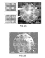
- FIGS. 2(a) and 2(b) are photographic images respectively showing an etched surface of a 6H-SiC crystal (initial stage of growth), and distribution of polytype inclusions in 6H-SiC boule (bulk growth stage);
- FIG. 3 is an image showing micropipe formation at 6H - 15R polytype boundaries.
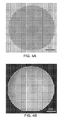
- FIGs. 4(a) - 4(c) are photographs respectively showing micropipe-free 4H - SiC substrates including an optical image of a 2-inch diameter wafer, a cross-polarized image of a 2-inch diameter wafer, and a cross-polarized image of a 3-inch diameter wafer according to various embodiments of the invention.
- FIG. 5 is a photograph showing a 100 mm diameter micropipe-free 4H - SiC wafer and fabricated in accordance with an embodiment of the invention.
- a SiC boule may be grown using a seeded sublimation growth process, such as PVT, using a seeded sublimation system.
- seeded sublimation systems may include high temperature CVD (HT-CVD) systems and halide CVD (H-CVD) systems.
- HT-CVD high temperature CVD
- H-CVD halide CVD
- a resulting SiC boule may then be sliced using conventional techniques into wafers, and the individual wafers may then be used as seed material for a seeded sublimation growth process, or as substrates upon which a variety of semiconductor devices may be formed.
- FIG. 1 is a cross sectional schematic diagram of a sublimation system 12 adapted for use in a seeded sublimation growth process of the type contemplated by certain embodiments of the invention.
- sublimation system 12 includes a carbon reaction crucible (also referred to as a susceptor or growth cell) 14 and a plurality of induction coils 16 adapted to heat reaction crucible 14 when electrical current is applied.
- a resistive heating approach may be applied to the heating of reaction crucible 14.
- the temperature within a furnace housing sublimation system 12 may be conventionally controllable.
- the furnace housing sublimation system 12 will also typically include one or more gas inlet and gas outlet ports and associated equipment allowing the controlled introduction and evacuation of gas from an environment surrounding reaction crucible 14.
- the introduction and evacuation of various gases to/from the environment surrounding reaction crucible 14 may be conventionally accomplished using a variety of inlets/outlets, pipes, valves, pumps, gas sources, and controllers.
- sublimation system 12 may further incorporate in certain embodiments a water-cooled quartz vessel. Such further elements are, however, less relevant to embodiments of the invention and are omitted as being known in the art.
- SiC sublimation systems of the type described herein are commercially available in various standard configurations. Alternately, sublimation systems may be designed and implemented in custom configurations, where necessary or appropriate. Accordingly, the method embodiments described herein are not limited to a particular subset of sublimation systems, or any particular system configuration. Rather, many different types and configurations of sublimation systems may be used to grow micropipe-free SiC material in accordance with an embodiment of the invention.
- reaction crucible 14 is surrounded by insulation material 18.
- insulation material 18 will vary with individual sublimation systems 12 in order to define and/or maintain desired thermal gradients (both axially and radially) in relation to reaction crucible 14.
- thermal gradient will be used herein to describe one or more thermal gradient(s) associated with reaction crucible 14.
- the thermal gradient established in embodiments of the invention will contain (or may be further characterized as having) axial and radial gradients, or may be characterized by a plurality of isotherms.
- reaction crucible 14 Prior to establishment of the thermal gradient, reaction crucible 14 is loaded with one or more source materials.
- Conventionally available reaction crucibles include one or more portions, as least one of which is capable of holding source material, such as powdered SiC 20. Powdered source material(s) are most commonly, but not exclusively, used in seeded sublimation growth processes.
- source material 20 is held in a lower portion of reaction crucible 14, as is common for one type of reaction crucible 14.
- Other competent reaction crucibles distribute source material in a vertical or cylindrical arrangement in which the source material surrounds a considerable portion of the interior of reaction crucible 14.
- reaction crucible 14 may be implemented in a number of different shapes, and may hold one or more source materials accordingly.
- embodiments of the invention may use conventional reaction crucible designs, the scope of the present invention is not limited to such designs, but will find application in different sublimation systems using many different types of reaction crucibles.
- Seed material 22 is placed above or in an upper portion of reaction crucible 14.
- Seed material 22 may take the form of a mono-crystalline SiC seed wafer having a diameter of about 2 inches, 3 inches (75 mm) or 4 inches (100 mm).
- a SiC single crystal boule 26 will be grown from seed material 22 during the seeded sublimation growth process.
- a seed holder 24 is used to hold seed material 22.
- Seed holder 24 is securely attached to reaction crucible 14 in an appropriate fashion using conventional techniques. For example, in the orientation illustrated in FIG. 1 , seed holder 24 is attached to an uppermost portion of reaction crucible 14 to hold seed material 22 in a desired position.
- seed holder 24 is fabricated from carbon.
- one or more type of dopant atoms may be intentionally introduced into sublimation system 12 during or before the seeded sublimation process.
- one or more dopant gases may be introduced into the seeded sublimation environment and thereby incorporated into the growing SiC crystalline boule.
- Dopants may be selected for their acceptor or donor capabilities in accordance with the conductivity properties desired for the resulting SiC boule.
- donor dopants produce n-type conductivity and acceptor dopants produce p-type conductivity.
- Some commonly incorporated n-type dopants include N, P, As, Sb, and/or Ti.
- Some commonly incorporated p-type dopants include B, AI, Ga, Be, Er, and/or Sc.
- an electrical current having a defined frequency to which the material (e.g., carbon) forming reaction crucible 14 will respond is passed through induction coils 16 to heat reaction crucible 14.
- the amount and placement of insulation material 18 are selected to create a thermal gradient between a source material 20 and a seed material 22.
- Reaction crucible 14 is heated with source material 20 to a sublimation temperature above about 2000°C, and typically ranging from about 2100°C to 2500°C. In this manner, a thermal gradient is established such that the temperature of seed material 22 and the SiC crystalline boule 26 growing on the seed material 22 remains slightly below the temperature of source material 20.
- certain vaporized species generated from the sublimating SiC source e.g., Si, Si 2 C and/or SiC 2
- Si, Si 2 C and/or SiC 2 are thermodynamically transported first to seed material 22 and thereafter to the growing SiC crystalline boule 26 (or "the SiC crystal").
- the crystal growth process is terminated by reducing the temperature of sublimation system 12 below about 1900°C and/or raising the pressure of the environment surrounding reaction crucible 14 above about 400 Torr.
- micropipes induced on the seed material and/or formed during growth are practically, if not completely, eliminated.
- micropipe-free 2-inch, 3-inch, and 100 mm diameter 4H-SiC crystals, as well as 2-inch and 3-inch 6H-SiC crystals have been demonstrated using various embodiments of the invention.
- foreign polytype nucleation such as 3C-polytype
- 3C-polytype typically occurs at the initial stages (nucleation period) and may even continue to nucleate during subsequent growth stages in the presence of the (0001) facet at the growth front, as shown in FIGs. 2(a) and 2(b) .
- 15R-polytype may nucleate on 3C-polytype inclusions both in 4H- and 6H-SiC boules. Instability in process parameters, such as pressure and temperature during the initial stage of growth, may cause polytype inclusion.
- facet boundaries which can form at different stages of the bulk growth process, increases the probability of polytype nucleation due to the reduced surface energy along these interfaces.
- Step-bunching and increased dislocation densities generally form along the [112 0] direction (and its family).
- the density of such defects increases further.
- the concentration of unintended impurities tends to increase in these areas, causing stress generation and lattice mismatch.
- facet boundaries and polytype inclusions extending from atomic levels to macroscopic scales, leads to increased defect levels including micropipe formation in SiC crystals. It should also be noted that the concentration and/or the composition of SiC source flux plays a critical role in forming defects discussed above. As such, the growth process parameters are carefully examined to find suitable conditions so that polytype inclusions and defect formation around such facet boundaries are reduced and/or prevented.
- FIG. 2(b) shows the 15R polytype inclusion in a 6H crystal occurring in the [11 2 0] direction and its family. This is confirmed by photoluminescence and UV absorption characteristics.
- FIG. 3 A cross-section of a 6H-SiC boule (cut along the c-axis direction) containing 15R-polytype inclusions is shown in FIG. 3 . Formation of micropipe clusters is shown on the 6H/15R boundaries.
- step bunching occurs at the facet border in the [11 2 0] direction;
- facet border is the preferred area for new polytype nucleation which generally propagates in the [11 2 0] direction(s);
- micropipe generation starts from polytype inclusions which are nucleated at polytype boundaries.
- the SiC boule is grown nominally in the c-axis direction, where the nominal c-axis direction is defined as being within the range of zero to 10 degrees from the c-axis [0001] direction.
- unintentional impurities within the system are targeted for elimination as a first possible source of micropipe nucleation.
- unintentional impurities on the seed or growth front may start to nucleate a micropipe and/or micropipe clusters that may propagate throughout the SiC boule.
- unintentional impurities within the source material may be eliminated by providing a very high quality SiC source material having as low an impurity content as possible.
- Common source material impurities include, as examples, iron, nickel and/or chromium. Where very high quality SiC source material of verified purity may be obtained, its incorporation within an embodiment of the invention is warranted.
- the SiC source material(s) being used contain a total concentration of less than 1 ppmwt of Ti, V, Cr, Mn, Fe, Co, Ni, Cu, Zn, Zr, Mo, Pd, Ta, and/or W.
- certain embodiments of the invention demand that the reaction crucible and seed material holder be fabricated from high quality, very pure carbon having as low a metal content as possible.
- the reduction of metallic impurities in the materials forming the source, reaction crucible, and seed holder may be confirmed using glow discharge mass spectroscopy (GDMS) and secondary ion mass spectroscopy (SIMS) analysis techniques.
- GDMS glow discharge mass spectroscopy
- SIMS secondary ion mass spectroscopy
- polytype inclusions are targeted as the remaining source for micropipe generation.
- the diffusion rate of the vapor species, growth temperature, pressure during bulk growth, source flux, ambient gases and growth zone dimensions such polytype inclusions may be eliminated.
- instabilities during crystal growth such as temperature spikes, pressure deviations or any changes in growth conditions, may cause polytype inclusions. Tight control of these processing parameters to maintain stable growth conditions eliminates polytype inclusions, thus preventing micropipe formation.
- growth pressure during an applied PVT process will range from about 0.1 to 400 Torr, and more typically between 0.1 and 100 Torr.
- the process temperature will range from about 2000°C to 2500°C. These conditions may vary due to differences in the sublimation system being used and variations in the seeded sublimation growth process being run.
- embodiments of the invention demand that the desired growth pressure and process temperature be strictly controlled without significant transients, in order to eliminate the occurrence of polytype inclusions and thereby prevent the formation of micropipes.
- certain embodiments of invention provide various methods of growing single-crystal SiC that is completely free of micropipe defects. These methods employ PVT to grow the SiC and generally provide for crystal growth along the nominal c-axis direction. However, embodiments of the invention are applicable to SiC crystal growth in a nominal direction within a range of from zero to 10 degrees from the c-axis direction. In one more specific embodiment, the growth direction is within 4 degrees of the c-axis direction with the tilt toward the [112 0] or the [1 1 00] direction.
- the seed may be implemented in wafer form from a material characterized by a micropipe density of less than 2 cm -2 , and more preferably by a micropipe density of less than 1 cm -2 .
- an acceptable SiC seed wafer may be characterized by one having a uniform x-ray diffraction exhibiting a full width at half maximum of less than 50 arcsec, and more preferably less than 30 arcsec.
- an acceptable SiC seed wafer is one characterized by no extraneous polytype inclusions.
- the attachment of the seed material i.e., a seed wafer
- a uniform thermal contact Various conventionally understood techniques may be used to implement a uniform thermal contact.
- the seed material may be placed in direct physical contact with the seed holder, or an adhesive may be used to fix the seed material to the seed holder, so as to ensure that conductive and/or radiative heat transfer is uniform over substantially the entire area between the seed and the seed holder.
- a wafer holder comprising a controlled gap structure may be used to define and maintain a desired separation gap between the seed material and the seed holder.
- a controlled gap structure requires a protective backside surface coating on the seed material (i.e., on the surface opposite to the growth surface) so that the seed material will not inadvertently sublimate during the growth process.
- a controlled gap structure may be used to form a separation distance between the seed material and seed holder of 10 ⁇ m or less, 5 ⁇ m or less, 2 ⁇ m or less, and where practically possible less than 1 ⁇ m.
- growth pressure is controlled in a range of about 300 to 0.1 torr, and more preferably in a range of about 50 to 0.1 torr.
- the process temperature is controlled in a range of about 2000 to 2500°C.
- the thermal gradient between the growing crystal and the source material is controlled in a range of about 50 to 150°C/cm.
- a sublimating SiC species flux during the process period may be controlled by a ramped increase in the growth temperature in the range of 0.3 to 10°C/hr.
- micropipes in single crystal SiC substrates can be reduced and/or eliminated by overgrown SiC epitaxy layers.
- This result may be achieved by controlling the input quantities of Si and C reactants, and thereby controlling the Si/C ratio during epitaxial growth.
- Such overgrowth under slightly silicon-rich conditions dissociates the large Burgers vector micropipes in the single crystal SiC substrate into a number of threading screw dislocations having smaller Burgers vectors that do not form open pipes structures in the resulting epitaxial layer.
- this particular micropipe reduction (elimination) mechanism may be extended to a sublimation growth method for bulk, as opposed to epitaxial, SiC crystals.
- This inventive extension proposes that at the beginning of the overall growth process (i.e., the growth nucleation phase), micropipes in seed material may be overgrown by; using a low micropipe density, but not necessarily micropipe-free seed material, and controlling the growth nucleation temperature, such that a modified Si/C ratio is induced by a low "start temperature" which promotes the closing-off of any micropipes existing in the seed material during the initial stages of bulk growth.
- this start temperature ranges between about 2000 to 2200°C.
- a sublimation process consistent with an embodiment of the invention may include the steps of first evacuating the environment around the reaction crucible to remove ambient air, gaseous impurities and extraneous solid particulates. Then, the reaction crucible is placed under pressure using one or more inert gas(es). Then, the sublimation system heats the reaction crucible environment to a temperature enabling SiC crystal growth via PVT. Once this temperature is reached, the pressure within the sublimation system is reduced to a point sufficient to initiate SiC crystal growth.
- Micropipe-free SiC crystals of various polytype may be grown including at least 3C, 4H, 6H, and 15R. Wafers cut from such SiC crystals may be subsequently used in the fabrication of various substrates. For example, using known techniques, high quality semiconductor wafers may be fabricated that include homo-epitaxial layers, such as SiC, as well as hetero-epitaxial layers, such as Group III-nitrides, on at least one surface thereof.
- the Group III-nitride layer may be, for example, GaN, AIGaN, AIN, AIInGaN, InN, and/or AIInN.
- semiconductor wafers may be fabricated that include a bulk single crystal SiC substrate having a diameter of at least 2 inches, 3 inches, 4 inches (100 mm) or larger and having a micropipe density of zero.
- the SiC substrate will include at least one and possibly two primary (and opposing) surfaces.
- a plurality of active and/or passive devices may be fabricated on the SiC substrate.
- an epitaxial layer may be formed on the primary surface of the substrate.
- This epitaxial layer may include a concentration of dopant atoms, sufficient to define a desired conductivity for the epitaxial layer.
- Source/drain regions may then be formed in the epitaxial layer to define channel regions for the devices.
- conventional semiconductor fabrication processes may be sequentially applied to the surface of the SiC wafer to form desired semiconductor devices, such as transistor(s) having conventional gate structure(s) (e.g., oxide or metal gate structures) formed over defined channel region(s).
- Selected examples of such transistors include; metal oxide semiconductor field-effect transistors, junction field-effect transistors, hetero-field-effect transistors, and metal semiconductor field-effect transistors.
- an epitaxial layer is formed on at least one primary surface of the substrate.
- the epitaxial layer may include selected concentration(s) of dopant atoms sufficient to define a desired conductivity for the epitaxial layer.
- the epitaxial layer may be used to fabricate one or more Schottky barrier diode(s), junction barrier Schottky diode(s), PiN diode(s), thyristor(s), and/or bipolar junction transistors on the epitaxial layer.
- micropipe-free substrates may be used to broaden the application of SiC material in the fabrication of semiconductor devices and electronic devices. It should be noted that the foregoing embodiments are not intended to be an exhaustive recitation of the scope of the subject invention. Rather, those skilled in the art will recognize that various modifications and adaptations to the foregoing may be made without departing from the scope of the invention as defined by the appended claims.
- any one of the foregoing method embodiments may be adapted to grow a Group III-nitride on seed material. That is, a single-crystal of Group III-nitride (Group III-nitride crystal) having a nominally c-axis growth direction may be grown using a physical vapor transport (PVT) process in a sublimation system. Such a Group III-nitride crystal will be completely free of micropipe defects.
- PVT physical vapor transport
- One method for growing a Group III-nitride crystal includes; attaching a seed material to a seed holder using a uniform thermal contact, placing a source material and the seed material attached to the seed holder in a reaction crucible associated with the sublimation system, wherein constituent components of the sublimation system including at least the source material, the seed holder, and the reaction crucible are substantially free from unintentional impurities, and controlling growth temperature, growth pressure, Group III-nitride sublimation flux and composition, and a temperature gradient between the source material and the seed material or the Group III-nitride crystal growing on the seed material during the PVT process to eliminate micropipe-inducing process instabilities and grow the micropipe-free Group III-nitride crystal on the seed material.
Landscapes
- Engineering & Computer Science (AREA)
- Chemical & Material Sciences (AREA)
- Power Engineering (AREA)
- Microelectronics & Electronic Packaging (AREA)
- Condensed Matter Physics & Semiconductors (AREA)
- General Physics & Mathematics (AREA)
- Computer Hardware Design (AREA)
- Physics & Mathematics (AREA)
- Manufacturing & Machinery (AREA)
- Crystallography & Structural Chemistry (AREA)
- Materials Engineering (AREA)
- Metallurgy (AREA)
- Organic Chemistry (AREA)
- Inorganic Chemistry (AREA)
- Ceramic Engineering (AREA)
- Crystals, And After-Treatments Of Crystals (AREA)
- Recrystallisation Techniques (AREA)
Applications Claiming Priority (2)
| Application Number | Priority Date | Filing Date | Title |
|---|---|---|---|
| US84436006P | 2006-09-14 | 2006-09-14 | |
| EP07842416.5A EP2059946B1 (fr) | 2006-09-14 | 2007-09-13 | Carbure de silicium exempt de micropipes et procede de fabrication associe |
Related Parent Applications (2)
| Application Number | Title | Priority Date | Filing Date |
|---|---|---|---|
| EP07842416.5A Division-Into EP2059946B1 (fr) | 2006-09-14 | 2007-09-13 | Carbure de silicium exempt de micropipes et procede de fabrication associe |
| EP07842416.5 Division | 2007-09-13 |
Publications (2)
| Publication Number | Publication Date |
|---|---|
| EP2264223A2 true EP2264223A2 (fr) | 2010-12-22 |
| EP2264223A3 EP2264223A3 (fr) | 2011-10-26 |
Family
ID=39184136
Family Applications (2)
| Application Number | Title | Priority Date | Filing Date |
|---|---|---|---|
| EP10182708A Ceased EP2264223A3 (fr) | 2006-09-14 | 2007-09-13 | Carbure de silicium sans micro-tuyaux et procédé de fabrication correspondant |
| EP07842416.5A Active EP2059946B1 (fr) | 2006-09-14 | 2007-09-13 | Carbure de silicium exempt de micropipes et procede de fabrication associe |
Family Applications After (1)
| Application Number | Title | Priority Date | Filing Date |
|---|---|---|---|
| EP07842416.5A Active EP2059946B1 (fr) | 2006-09-14 | 2007-09-13 | Carbure de silicium exempt de micropipes et procede de fabrication associe |
Country Status (5)
| Country | Link |
|---|---|
| US (3) | US8410488B2 (fr) |
| EP (2) | EP2264223A3 (fr) |
| JP (2) | JP5562641B2 (fr) |
| CN (1) | CN101536168A (fr) |
| WO (1) | WO2008033994A1 (fr) |
Cited By (9)
| Publication number | Priority date | Publication date | Assignee | Title |
|---|---|---|---|---|
| US8940614B2 (en) | 2013-03-15 | 2015-01-27 | Dow Corning Corporation | SiC substrate with SiC epitaxial film |
| US9017804B2 (en) | 2013-02-05 | 2015-04-28 | Dow Corning Corporation | Method to reduce dislocations in SiC crystal growth |
| US9018639B2 (en) | 2012-10-26 | 2015-04-28 | Dow Corning Corporation | Flat SiC semiconductor substrate |
| US9279192B2 (en) | 2014-07-29 | 2016-03-08 | Dow Corning Corporation | Method for manufacturing SiC wafer fit for integration with power device manufacturing technology |
| US9337277B2 (en) | 2012-09-11 | 2016-05-10 | Dow Corning Corporation | High voltage power semiconductor device on SiC |
| US9738991B2 (en) | 2013-02-05 | 2017-08-22 | Dow Corning Corporation | Method for growing a SiC crystal by vapor deposition onto a seed crystal provided on a supporting shelf which permits thermal expansion |
| US9797064B2 (en) | 2013-02-05 | 2017-10-24 | Dow Corning Corporation | Method for growing a SiC crystal by vapor deposition onto a seed crystal provided on a support shelf which permits thermal expansion |
| CN108411368A (zh) * | 2018-06-11 | 2018-08-17 | 山东大学 | 一种快速有选择性的降低SiC晶体中微管和位错密度的方法 |
| WO2022123078A1 (fr) * | 2020-12-11 | 2022-06-16 | Zadient Technologies SAS | Procédé et dispositif de production d'un matériau solide de sic |
Families Citing this family (45)
| Publication number | Priority date | Publication date | Assignee | Title |
|---|---|---|---|---|
| US7314520B2 (en) * | 2004-10-04 | 2008-01-01 | Cree, Inc. | Low 1c screw dislocation 3 inch silicon carbide wafer |
| EP2264223A3 (fr) * | 2006-09-14 | 2011-10-26 | Cree, Inc. | Carbure de silicium sans micro-tuyaux et procédé de fabrication correspondant |
| US7994027B2 (en) * | 2008-05-09 | 2011-08-09 | George Mason Intellectual Properties, Inc. | Microwave heating for semiconductor nanostructure fabrication |
| WO2010077639A2 (fr) * | 2008-12-08 | 2010-07-08 | Ii-Vi Incorporated | Procédé et appareil perfectionnés de croissance par transport à gradient axial (agt) utilisant un chauffage par effet joule |
| JP5565070B2 (ja) * | 2010-04-26 | 2014-08-06 | 住友電気工業株式会社 | 炭化珪素結晶および炭化珪素結晶の製造方法 |
| US8377806B2 (en) * | 2010-04-28 | 2013-02-19 | Cree, Inc. | Method for controlled growth of silicon carbide and structures produced by same |
| JP2011243770A (ja) * | 2010-05-19 | 2011-12-01 | Sumitomo Electric Ind Ltd | 炭化珪素基板、半導体装置、炭化珪素基板の製造方法 |
| US8445386B2 (en) * | 2010-05-27 | 2013-05-21 | Cree, Inc. | Smoothing method for semiconductor material and wafers produced by same |
| JP5696630B2 (ja) * | 2011-09-21 | 2015-04-08 | 住友電気工業株式会社 | 炭化珪素基板およびその製造方法 |
| JP6226959B2 (ja) * | 2012-04-20 | 2017-11-08 | トゥー‐シックス・インコーポレイテッド | 大口径高品質SiC単結晶、方法、及び装置 |
| US9041010B2 (en) * | 2012-05-29 | 2015-05-26 | William F. Seng | Wide band gap semiconductor wafers grown and processed in a microgravity environment and method of production |
| KR101926694B1 (ko) * | 2012-05-30 | 2018-12-07 | 엘지이노텍 주식회사 | 탄화규소 에피 웨이퍼 및 이의 제조 방법 |
| KR101926678B1 (ko) * | 2012-05-31 | 2018-12-11 | 엘지이노텍 주식회사 | 탄화규소 에피 웨이퍼 및 이의 제조 방법 |
| JP2014024703A (ja) * | 2012-07-26 | 2014-02-06 | Sumitomo Electric Ind Ltd | 炭化珪素単結晶の製造方法 |
| JP5991161B2 (ja) * | 2012-11-20 | 2016-09-14 | 住友電気工業株式会社 | 炭化珪素基板および炭化珪素インゴット、ならびにこれらの製造方法 |
| US9657409B2 (en) | 2013-05-02 | 2017-05-23 | Melior Innovations, Inc. | High purity SiOC and SiC, methods compositions and applications |
| US9919972B2 (en) | 2013-05-02 | 2018-03-20 | Melior Innovations, Inc. | Pressed and self sintered polymer derived SiC materials, applications and devices |
| US10322936B2 (en) | 2013-05-02 | 2019-06-18 | Pallidus, Inc. | High purity polysilocarb materials, applications and processes |
| US11091370B2 (en) | 2013-05-02 | 2021-08-17 | Pallidus, Inc. | Polysilocarb based silicon carbide materials, applications and devices |
| JP6183010B2 (ja) * | 2013-07-03 | 2017-08-23 | 住友電気工業株式会社 | 炭化珪素単結晶基板およびその製造方法 |
| KR101669444B1 (ko) * | 2014-02-13 | 2016-10-26 | 한국전기연구원 | 액상 기법을 이용한 SiC 단결정 성장 방법 |
| US9422639B2 (en) | 2014-03-06 | 2016-08-23 | Sumitomo Electric Industries, Ltd. | Silicon carbide substrate, silicon carbide ingot, and methods for manufacturing silicon carbide substrate and silicon carbide ingot |
| WO2015182246A1 (fr) * | 2014-05-29 | 2015-12-03 | 住友電気工業株式会社 | Procédé de fabrication de lingot de carbure de silicium, substrat germe en carbure de silicium et substrat en carbure de silicium |
| CN104357912B (zh) * | 2014-12-07 | 2016-09-21 | 中国电子科技集团公司第四十六研究所 | 一种感应加热炉内的钨坩埚保护方法 |
| JP6036947B2 (ja) * | 2015-09-02 | 2016-11-30 | 住友電気工業株式会社 | 炭化珪素基板および炭化珪素インゴットの製造方法 |
| WO2017057742A1 (fr) * | 2015-10-02 | 2017-04-06 | 新日鐵住金株式会社 | Lingot monocristallin de sic |
| US20170137962A1 (en) * | 2015-11-16 | 2017-05-18 | National Chung-Shan Institute Of Science And Technology | Fabrication Method for Growing Single Crystal of Multi-Type Compound |
| US11320388B2 (en) | 2016-08-31 | 2022-05-03 | Showa Denko K.K. | SiC epitaxial wafer containing large pit defects with a surface density of 0.5 defects/CM2 or less, and production method therefor |
| WO2018043171A1 (fr) * | 2016-08-31 | 2018-03-08 | 昭和電工株式会社 | Tranche épitaxiale de sic, son procédé de production et procédé d'identification de défaut |
| JP6459132B2 (ja) * | 2016-08-31 | 2019-01-30 | 昭和電工株式会社 | SiCエピタキシャルウェハ及びその製造方法、並びに、欠陥識別方法 |
| CN106894090B (zh) * | 2017-03-17 | 2019-09-24 | 山东大学 | 一种高质量低电阻率的p型SiC单晶制备方法 |
| CN106968018B (zh) * | 2017-04-10 | 2019-02-05 | 山东大学 | 一种锗氮共掺的碳化硅单晶材料的生长方法 |
| CN107190323A (zh) * | 2017-06-06 | 2017-09-22 | 宝鸡文理学院 | 一种生长低缺陷碳化硅单晶的方法 |
| CN107699955A (zh) * | 2017-08-30 | 2018-02-16 | 昆明理工大学 | 一种利用微波加热去除碳化硅单晶缺陷中及表面有机杂质的方法 |
| CN107460547B (zh) * | 2017-09-12 | 2019-11-15 | 中国电子科技集团公司第四十六研究所 | 一种pvt法氮化铝晶体生长炉用复合保温屏及生成方法 |
| JP6881365B2 (ja) * | 2018-03-16 | 2021-06-02 | 信越半導体株式会社 | 炭化珪素単結晶の製造方法及び製造装置 |
| CN108977886A (zh) * | 2018-08-20 | 2018-12-11 | 孙月静 | 一种SiC晶体的制造方法 |
| US11453957B2 (en) | 2018-12-07 | 2022-09-27 | Showa Denko K.K. | Crystal growing apparatus and crucible having a main body portion and a first portion having a radiation rate different from that of the main body portion |
| JP7148427B2 (ja) * | 2019-02-06 | 2022-10-05 | 昭和電工株式会社 | SiCエピタキシャルウェハ及びその製造方法 |
| CN110042470A (zh) * | 2019-04-29 | 2019-07-23 | 南通大学 | 一种多尺寸莫桑石的制备方法 |
| CN110670123B (zh) * | 2019-09-23 | 2021-03-26 | 河北同光晶体有限公司 | 一种延续单一生长中心制备碳化硅单晶的方法 |
| KR102284879B1 (ko) | 2019-10-29 | 2021-07-30 | 에스케이씨 주식회사 | 탄화규소 웨이퍼 및 탄화규소 웨이퍼의 제조방법 |
| CN110919465A (zh) * | 2019-11-08 | 2020-03-27 | 中国科学院上海硅酸盐研究所 | 无损伤、高平面度单晶碳化硅平面光学元件及其制备方法 |
| CN110983434B (zh) * | 2019-12-27 | 2021-04-16 | 北京天科合达半导体股份有限公司 | 一种有效降低碳化硅单晶缺陷的生长方法和高质量碳化硅单晶 |
| KR102192518B1 (ko) | 2020-07-14 | 2020-12-17 | 에스케이씨 주식회사 | 웨이퍼 및 웨이퍼의 제조방법 |
Citations (3)
| Publication number | Priority date | Publication date | Assignee | Title |
|---|---|---|---|---|
| US4866005A (en) | 1987-10-26 | 1989-09-12 | North Carolina State University | Sublimation of silicon carbide to produce large, device quality single crystals of silicon carbide |
| US4912064A (en) | 1987-10-26 | 1990-03-27 | North Carolina State University | Homoepitaxial growth of alpha-SiC thin films and semiconductor devices fabricated thereon |
| US5679153A (en) | 1994-11-30 | 1997-10-21 | Cree Research, Inc. | Method for reducing micropipe formation in the epitaxial growth of silicon carbide and resulting silicon carbide structures |
Family Cites Families (29)
| Publication number | Priority date | Publication date | Assignee | Title |
|---|---|---|---|---|
| US34861A (en) | 1862-04-01 | Improved washing-machine | ||
| US6344663B1 (en) * | 1992-06-05 | 2002-02-05 | Cree, Inc. | Silicon carbide CMOS devices |
| US5718760A (en) * | 1996-02-05 | 1998-02-17 | Cree Research, Inc. | Growth of colorless silicon carbide crystals |
| US5873937A (en) * | 1997-05-05 | 1999-02-23 | Northrop Grumman Corporation | Method of growing 4H silicon carbide crystal |
| JP3043689B2 (ja) | 1997-11-17 | 2000-05-22 | 日本ピラー工業株式会社 | 単結晶SiC及びその製造方法 |
| JP2000044395A (ja) * | 1998-07-29 | 2000-02-15 | Toyota Central Res & Dev Lab Inc | 炭化珪素単結晶の製造方法 |
| DE60033829T2 (de) * | 1999-09-07 | 2007-10-11 | Sixon Inc. | SiC-HALBLEITERSCHEIBE, SiC-HALBLEITERBAUELEMENT SOWIE HERSTELLUNGSVERFAHREN FÜR EINE SiC-HALBLEITERSCHEIBE |
| FR2816113A1 (fr) * | 2000-10-31 | 2002-05-03 | St Microelectronics Sa | Procede de realisation d'une zone dopee dans du carbure de silicium et application a une diode schottky |
| JP4903946B2 (ja) * | 2000-12-28 | 2012-03-28 | 株式会社ブリヂストン | 炭化ケイ素単結晶の製造方法及び製造装置 |
| JP4830073B2 (ja) | 2001-03-27 | 2011-12-07 | 独立行政法人産業技術総合研究所 | 炭化珪素単結晶の成長方法 |
| JP4942255B2 (ja) | 2001-05-08 | 2012-05-30 | 三菱電機株式会社 | 炭化珪素半導体装置およびその製造方法 |
| DE10247017B4 (de) * | 2001-10-12 | 2009-06-10 | Denso Corp., Kariya-shi | SiC-Einkristall, Verfahren zur Herstellung eines SiC-Einkristalls, SiC-Wafer mit einem Epitaxiefilm und Verfahren zur Herstellung eines SiC-Wafers, der einen Epitaxiefilm aufweist |
| DE60335252D1 (de) * | 2002-04-04 | 2011-01-20 | Nippon Steel Corp | Impfkristall aus siliciumcarbid-einkristall und verfahren zur herstellung eines stabs damit |
| US6814801B2 (en) * | 2002-06-24 | 2004-11-09 | Cree, Inc. | Method for producing semi-insulating resistivity in high purity silicon carbide crystals |
| US7601441B2 (en) * | 2002-06-24 | 2009-10-13 | Cree, Inc. | One hundred millimeter high purity semi-insulating single crystal silicon carbide wafer |
| JP2004200188A (ja) | 2002-12-16 | 2004-07-15 | Shin Etsu Handotai Co Ltd | ヘテロエピタキシャルウエーハおよびその製造方法 |
| TWI320948B (en) | 2003-03-19 | 2010-02-21 | Japan Science & Tech Agency | Method for growing emiconductor crystal and laminated structure thereof and semiconductor device |
| JP4480349B2 (ja) * | 2003-05-30 | 2010-06-16 | 株式会社ブリヂストン | 炭化ケイ素単結晶の製造方法及び製造装置 |
| TWI313060B (en) * | 2003-07-28 | 2009-08-01 | Japan Science & Tech Agency | Feild effect transisitor and fabricating method thereof |
| JP4635470B2 (ja) | 2004-04-19 | 2011-02-23 | 株式会社デンソー | 炭化珪素半導体装置およびその製造方法 |
| DE102005017814B4 (de) | 2004-04-19 | 2016-08-11 | Denso Corporation | Siliziumkarbid-Halbleiterbauelement und Verfahren zu dessen Herstellung |
| JP4494856B2 (ja) | 2004-04-28 | 2010-06-30 | 新日本製鐵株式会社 | 炭化珪素単結晶成長用種結晶とその製造方法及びそれを用いた結晶成長方法 |
| JP4708746B2 (ja) * | 2004-09-02 | 2011-06-22 | 株式会社ブリヂストン | 炭化ケイ素単結晶の製造方法及び製造装置 |
| US7294324B2 (en) * | 2004-09-21 | 2007-11-13 | Cree, Inc. | Low basal plane dislocation bulk grown SiC wafers |
| US7314520B2 (en) | 2004-10-04 | 2008-01-01 | Cree, Inc. | Low 1c screw dislocation 3 inch silicon carbide wafer |
| US7314521B2 (en) | 2004-10-04 | 2008-01-01 | Cree, Inc. | Low micropipe 100 mm silicon carbide wafer |
| JP4586547B2 (ja) | 2005-01-24 | 2010-11-24 | 住友電気工業株式会社 | 接合型電界効果トランジスタ |
| US7387680B2 (en) * | 2005-05-13 | 2008-06-17 | Cree, Inc. | Method and apparatus for the production of silicon carbide crystals |
| EP2264223A3 (fr) | 2006-09-14 | 2011-10-26 | Cree, Inc. | Carbure de silicium sans micro-tuyaux et procédé de fabrication correspondant |
-
2007
- 2007-09-13 EP EP10182708A patent/EP2264223A3/fr not_active Ceased
- 2007-09-13 US US11/854,878 patent/US8410488B2/en active Active
- 2007-09-13 WO PCT/US2007/078385 patent/WO2008033994A1/fr active Application Filing
- 2007-09-13 JP JP2009528471A patent/JP5562641B2/ja active Active
- 2007-09-13 EP EP07842416.5A patent/EP2059946B1/fr active Active
- 2007-09-13 CN CNA2007800421901A patent/CN101536168A/zh active Pending
- 2007-09-13 US US11/854,864 patent/US9099377B2/en active Active
-
2013
- 2013-03-04 US US13/784,083 patent/US20130181231A1/en not_active Abandoned
-
2014
- 2014-06-05 JP JP2014116662A patent/JP2014221711A/ja active Pending
Patent Citations (4)
| Publication number | Priority date | Publication date | Assignee | Title |
|---|---|---|---|---|
| US4866005A (en) | 1987-10-26 | 1989-09-12 | North Carolina State University | Sublimation of silicon carbide to produce large, device quality single crystals of silicon carbide |
| US4912064A (en) | 1987-10-26 | 1990-03-27 | North Carolina State University | Homoepitaxial growth of alpha-SiC thin films and semiconductor devices fabricated thereon |
| USRE34861E (en) | 1987-10-26 | 1995-02-14 | North Carolina State University | Sublimation of silicon carbide to produce large, device quality single crystals of silicon carbide |
| US5679153A (en) | 1994-11-30 | 1997-10-21 | Cree Research, Inc. | Method for reducing micropipe formation in the epitaxial growth of silicon carbide and resulting silicon carbide structures |
Non-Patent Citations (4)
| Title |
|---|
| J. SUMAKERIS ET AL., 5TH EUROPEAN CONFERENCE ON SILICON CARBIDE AND RELATED MATERIALS, 2004 |
| KUHR ET AL.: "Hexagonal voids and the formation of micropipes during SiC sublimation growth", JOURNAL OF APPLIED PHYSICS, vol. 89, no. 8, April 2001 (2001-04-01), pages 4625 |
| NAKAMURA ET AL.: "Ultrahigh quality silicon carbide single crystals", NATURE, vol. 430, 26 August 2004 (2004-08-26), pages 1009 |
| POWELL ET AL.: "rowth of low micropipe density SiC wafers", MATERIALS SCIENCE FORUM, vol. 338-40, 2000, pages 437 - 40 |
Cited By (11)
| Publication number | Priority date | Publication date | Assignee | Title |
|---|---|---|---|---|
| US9337277B2 (en) | 2012-09-11 | 2016-05-10 | Dow Corning Corporation | High voltage power semiconductor device on SiC |
| US9018639B2 (en) | 2012-10-26 | 2015-04-28 | Dow Corning Corporation | Flat SiC semiconductor substrate |
| US9165779B2 (en) | 2012-10-26 | 2015-10-20 | Dow Corning Corporation | Flat SiC semiconductor substrate |
| US9017804B2 (en) | 2013-02-05 | 2015-04-28 | Dow Corning Corporation | Method to reduce dislocations in SiC crystal growth |
| US9738991B2 (en) | 2013-02-05 | 2017-08-22 | Dow Corning Corporation | Method for growing a SiC crystal by vapor deposition onto a seed crystal provided on a supporting shelf which permits thermal expansion |
| US9797064B2 (en) | 2013-02-05 | 2017-10-24 | Dow Corning Corporation | Method for growing a SiC crystal by vapor deposition onto a seed crystal provided on a support shelf which permits thermal expansion |
| US8940614B2 (en) | 2013-03-15 | 2015-01-27 | Dow Corning Corporation | SiC substrate with SiC epitaxial film |
| US9279192B2 (en) | 2014-07-29 | 2016-03-08 | Dow Corning Corporation | Method for manufacturing SiC wafer fit for integration with power device manufacturing technology |
| US10002760B2 (en) | 2014-07-29 | 2018-06-19 | Dow Silicones Corporation | Method for manufacturing SiC wafer fit for integration with power device manufacturing technology |
| CN108411368A (zh) * | 2018-06-11 | 2018-08-17 | 山东大学 | 一种快速有选择性的降低SiC晶体中微管和位错密度的方法 |
| WO2022123078A1 (fr) * | 2020-12-11 | 2022-06-16 | Zadient Technologies SAS | Procédé et dispositif de production d'un matériau solide de sic |
Also Published As
| Publication number | Publication date |
|---|---|
| WO2008033994A1 (fr) | 2008-03-20 |
| EP2264223A3 (fr) | 2011-10-26 |
| EP2059946B1 (fr) | 2019-12-11 |
| US20080067524A1 (en) | 2008-03-20 |
| JP5562641B2 (ja) | 2014-07-30 |
| US20130181231A1 (en) | 2013-07-18 |
| CN101536168A (zh) | 2009-09-16 |
| EP2059946A1 (fr) | 2009-05-20 |
| US9099377B2 (en) | 2015-08-04 |
| JP2010514648A (ja) | 2010-05-06 |
| EP2059946A4 (fr) | 2011-10-26 |
| JP2014221711A (ja) | 2014-11-27 |
| US8410488B2 (en) | 2013-04-02 |
| US20080083366A1 (en) | 2008-04-10 |
Similar Documents
| Publication | Publication Date | Title |
|---|---|---|
| EP2059946B1 (fr) | Carbure de silicium exempt de micropipes et procede de fabrication associe | |
| EP1797225B2 (fr) | Tranche de carbure de silicium de 3 pouces et a faible dislocation en vis 1c | |
| EP1888821B1 (fr) | Galettes de sic développées en paquets à faible dislocation de plan basal | |
| JP5680269B2 (ja) | 低マイクロパイプの100mm炭化ケイ素ウェハ | |
| US20100031877A1 (en) | Sic single crystals with reduced dislocation density grown by step-wise periodic perturbation technique | |
| JP4818754B2 (ja) | 炭化珪素単結晶インゴットの製造方法 | |
| JP2004099340A (ja) | 炭化珪素単結晶育成用種結晶と炭化珪素単結晶インゴット及びその製造方法 | |
| JP2009102187A (ja) | 炭化珪素単結晶育成用坩堝、及びこれを用いた炭化珪素単結晶の製造方法、並びに炭化珪素単結晶インゴット |
Legal Events
| Date | Code | Title | Description |
|---|---|---|---|
| PUAI | Public reference made under article 153(3) epc to a published international application that has entered the european phase |
Free format text: ORIGINAL CODE: 0009012 |
|
| AC | Divisional application: reference to earlier application |
Ref document number: 2059946 Country of ref document: EP Kind code of ref document: P |
|
| AK | Designated contracting states |
Kind code of ref document: A2 Designated state(s): AT BE BG CH CY CZ DE DK EE ES FI FR GB GR HU IE IS IT LI LT LU LV MC MT NL PL PT RO SE SI SK TR |
|
| RIN1 | Information on inventor provided before grant (corrected) |
Inventor name: BASCERI, CEM Inventor name: HOBGOOD, HUDSON MCD Inventor name: SILAN, MURAT N Inventor name: LEONARD, ROBERT T Inventor name: KHLEBNIKOV, IGOR Inventor name: JENNY, JASON R Inventor name: TSVETKOV, VALERI Inventor name: POWELL, ADRIAN R Inventor name: BALAKRISHNA, VIJAY Inventor name: CARTER, CALVIN H., JR. Inventor name: BALKAS, CENGIZ Inventor name: KHLEBNIKOV, YURI |
|
| PUAL | Search report despatched |
Free format text: ORIGINAL CODE: 0009013 |
|
| AK | Designated contracting states |
Kind code of ref document: A3 Designated state(s): AT BE BG CH CY CZ DE DK EE ES FI FR GB GR HU IE IS IT LI LT LU LV MC MT NL PL PT RO SE SI SK TR |
|
| RIC1 | Information provided on ipc code assigned before grant |
Ipc: C30B 23/00 20060101AFI20110920BHEP Ipc: H01L 21/20 20060101ALI20110920BHEP Ipc: H01L 21/02 20060101ALI20110920BHEP Ipc: C30B 29/36 20060101ALI20110920BHEP |
|
| 17P | Request for examination filed |
Effective date: 20120425 |
|
| 17Q | First examination report despatched |
Effective date: 20120525 |
|
| STAA | Information on the status of an ep patent application or granted ep patent |
Free format text: STATUS: THE APPLICATION HAS BEEN REFUSED |
|
| 18R | Application refused |
Effective date: 20160123 |