JP5565070B2 - 炭化珪素結晶および炭化珪素結晶の製造方法 - Google Patents
炭化珪素結晶および炭化珪素結晶の製造方法 Download PDFInfo
- Publication number
- JP5565070B2 JP5565070B2 JP2010100891A JP2010100891A JP5565070B2 JP 5565070 B2 JP5565070 B2 JP 5565070B2 JP 2010100891 A JP2010100891 A JP 2010100891A JP 2010100891 A JP2010100891 A JP 2010100891A JP 5565070 B2 JP5565070 B2 JP 5565070B2
- Authority
- JP
- Japan
- Prior art keywords
- raw material
- sic crystal
- silicon carbide
- crystal
- carbide crystal
- Prior art date
- Legal status (The legal status is an assumption and is not a legal conclusion. Google has not performed a legal analysis and makes no representation as to the accuracy of the status listed.)
- Active
Links
- 239000013078 crystal Substances 0.000 title claims description 220
- 229910010271 silicon carbide Inorganic materials 0.000 title claims description 220
- HBMJWWWQQXIZIP-UHFFFAOYSA-N silicon carbide Chemical compound [Si+]#[C-] HBMJWWWQQXIZIP-UHFFFAOYSA-N 0.000 title claims description 216
- 238000004519 manufacturing process Methods 0.000 title claims description 35
- 239000002994 raw material Substances 0.000 claims description 129
- 239000002245 particle Substances 0.000 claims description 47
- XEEYBQQBJWHFJM-UHFFFAOYSA-N Iron Chemical compound [Fe] XEEYBQQBJWHFJM-UHFFFAOYSA-N 0.000 claims description 34
- 239000000758 substrate Substances 0.000 claims description 29
- 238000009826 distribution Methods 0.000 claims description 22
- 238000000034 method Methods 0.000 claims description 21
- 229910052782 aluminium Inorganic materials 0.000 claims description 18
- 238000010438 heat treatment Methods 0.000 claims description 17
- 229910052742 iron Inorganic materials 0.000 claims description 17
- 238000005498 polishing Methods 0.000 claims description 6
- 230000001376 precipitating effect Effects 0.000 claims description 6
- 239000003929 acidic solution Substances 0.000 claims description 5
- XAGFODPZIPBFFR-UHFFFAOYSA-N aluminium Chemical compound [Al] XAGFODPZIPBFFR-UHFFFAOYSA-N 0.000 claims description 3
- 238000005406 washing Methods 0.000 claims description 2
- 239000012535 impurity Substances 0.000 description 26
- KWYUFKZDYYNOTN-UHFFFAOYSA-M Potassium hydroxide Chemical compound [OH-].[K+] KWYUFKZDYYNOTN-UHFFFAOYSA-M 0.000 description 10
- 230000000052 comparative effect Effects 0.000 description 9
- 239000007789 gas Substances 0.000 description 9
- 230000006866 deterioration Effects 0.000 description 6
- 238000010298 pulverizing process Methods 0.000 description 6
- 239000004065 semiconductor Substances 0.000 description 6
- 101000878457 Macrocallista nimbosa FMRFamide Proteins 0.000 description 5
- IJGRMHOSHXDMSA-UHFFFAOYSA-N Atomic nitrogen Chemical compound N#N IJGRMHOSHXDMSA-UHFFFAOYSA-N 0.000 description 4
- VEXZGXHMUGYJMC-UHFFFAOYSA-N Hydrochloric acid Chemical compound Cl VEXZGXHMUGYJMC-UHFFFAOYSA-N 0.000 description 4
- 239000000843 powder Substances 0.000 description 4
- ZOXJGFHDIHLPTG-UHFFFAOYSA-N Boron Chemical compound [B] ZOXJGFHDIHLPTG-UHFFFAOYSA-N 0.000 description 3
- QZPSXPBJTPJTSZ-UHFFFAOYSA-N aqua regia Chemical compound Cl.O[N+]([O-])=O QZPSXPBJTPJTSZ-UHFFFAOYSA-N 0.000 description 3
- 229910052796 boron Inorganic materials 0.000 description 3
- 238000005520 cutting process Methods 0.000 description 3
- 230000007547 defect Effects 0.000 description 3
- 238000000227 grinding Methods 0.000 description 3
- 238000000859 sublimation Methods 0.000 description 3
- 230000008022 sublimation Effects 0.000 description 3
- OKTJSMMVPCPJKN-UHFFFAOYSA-N Carbon Chemical compound [C] OKTJSMMVPCPJKN-UHFFFAOYSA-N 0.000 description 2
- 238000001636 atomic emission spectroscopy Methods 0.000 description 2
- 230000015556 catabolic process Effects 0.000 description 2
- 238000001514 detection method Methods 0.000 description 2
- 238000011156 evaluation Methods 0.000 description 2
- 238000011049 filling Methods 0.000 description 2
- 229910002804 graphite Inorganic materials 0.000 description 2
- 239000010439 graphite Substances 0.000 description 2
- 229910001385 heavy metal Inorganic materials 0.000 description 2
- 229910052757 nitrogen Inorganic materials 0.000 description 2
- 230000000149 penetrating effect Effects 0.000 description 2
- 239000007858 starting material Substances 0.000 description 2
- 238000005092 sublimation method Methods 0.000 description 2
- MKYBYDHXWVHEJW-UHFFFAOYSA-N N-[1-oxo-1-(2,4,6,7-tetrahydrotriazolo[4,5-c]pyridin-5-yl)propan-2-yl]-2-[[3-(trifluoromethoxy)phenyl]methylamino]pyrimidine-5-carboxamide Chemical compound O=C(C(C)NC(=O)C=1C=NC(=NC=1)NCC1=CC(=CC=C1)OC(F)(F)F)N1CC2=C(CC1)NN=N2 MKYBYDHXWVHEJW-UHFFFAOYSA-N 0.000 description 1
- XUIMIQQOPSSXEZ-UHFFFAOYSA-N Silicon Chemical compound [Si] XUIMIQQOPSSXEZ-UHFFFAOYSA-N 0.000 description 1
- 239000003082 abrasive agent Substances 0.000 description 1
- 239000003575 carbonaceous material Substances 0.000 description 1
- 238000003776 cleavage reaction Methods 0.000 description 1
- 238000010586 diagram Methods 0.000 description 1
- 230000000694 effects Effects 0.000 description 1
- 230000005684 electric field Effects 0.000 description 1
- 238000005530 etching Methods 0.000 description 1
- 238000007654 immersion Methods 0.000 description 1
- 230000001939 inductive effect Effects 0.000 description 1
- 238000002354 inductively-coupled plasma atomic emission spectroscopy Methods 0.000 description 1
- 239000000463 material Substances 0.000 description 1
- 238000012986 modification Methods 0.000 description 1
- 230000004048 modification Effects 0.000 description 1
- 230000007017 scission Effects 0.000 description 1
- 238000007790 scraping Methods 0.000 description 1
- 229910052710 silicon Inorganic materials 0.000 description 1
- 239000010703 silicon Substances 0.000 description 1
- 239000002210 silicon-based material Substances 0.000 description 1
- 239000000126 substance Substances 0.000 description 1
Images


Classifications
-
- C—CHEMISTRY; METALLURGY
- C30—CRYSTAL GROWTH
- C30B—SINGLE-CRYSTAL GROWTH; UNIDIRECTIONAL SOLIDIFICATION OF EUTECTIC MATERIAL OR UNIDIRECTIONAL DEMIXING OF EUTECTOID MATERIAL; REFINING BY ZONE-MELTING OF MATERIAL; PRODUCTION OF A HOMOGENEOUS POLYCRYSTALLINE MATERIAL WITH DEFINED STRUCTURE; SINGLE CRYSTALS OR HOMOGENEOUS POLYCRYSTALLINE MATERIAL WITH DEFINED STRUCTURE; AFTER-TREATMENT OF SINGLE CRYSTALS OR A HOMOGENEOUS POLYCRYSTALLINE MATERIAL WITH DEFINED STRUCTURE; APPARATUS THEREFOR
- C30B23/00—Single-crystal growth by condensing evaporated or sublimed materials
- C30B23/02—Epitaxial-layer growth
- C30B23/06—Heating of the deposition chamber, the substrate or the materials to be evaporated
-
- C—CHEMISTRY; METALLURGY
- C30—CRYSTAL GROWTH
- C30B—SINGLE-CRYSTAL GROWTH; UNIDIRECTIONAL SOLIDIFICATION OF EUTECTIC MATERIAL OR UNIDIRECTIONAL DEMIXING OF EUTECTOID MATERIAL; REFINING BY ZONE-MELTING OF MATERIAL; PRODUCTION OF A HOMOGENEOUS POLYCRYSTALLINE MATERIAL WITH DEFINED STRUCTURE; SINGLE CRYSTALS OR HOMOGENEOUS POLYCRYSTALLINE MATERIAL WITH DEFINED STRUCTURE; AFTER-TREATMENT OF SINGLE CRYSTALS OR A HOMOGENEOUS POLYCRYSTALLINE MATERIAL WITH DEFINED STRUCTURE; APPARATUS THEREFOR
- C30B23/00—Single-crystal growth by condensing evaporated or sublimed materials
- C30B23/02—Epitaxial-layer growth
- C30B23/025—Epitaxial-layer growth characterised by the substrate
-
- C—CHEMISTRY; METALLURGY
- C30—CRYSTAL GROWTH
- C30B—SINGLE-CRYSTAL GROWTH; UNIDIRECTIONAL SOLIDIFICATION OF EUTECTIC MATERIAL OR UNIDIRECTIONAL DEMIXING OF EUTECTOID MATERIAL; REFINING BY ZONE-MELTING OF MATERIAL; PRODUCTION OF A HOMOGENEOUS POLYCRYSTALLINE MATERIAL WITH DEFINED STRUCTURE; SINGLE CRYSTALS OR HOMOGENEOUS POLYCRYSTALLINE MATERIAL WITH DEFINED STRUCTURE; AFTER-TREATMENT OF SINGLE CRYSTALS OR A HOMOGENEOUS POLYCRYSTALLINE MATERIAL WITH DEFINED STRUCTURE; APPARATUS THEREFOR
- C30B23/00—Single-crystal growth by condensing evaporated or sublimed materials
- C30B23/02—Epitaxial-layer growth
-
- C—CHEMISTRY; METALLURGY
- C30—CRYSTAL GROWTH
- C30B—SINGLE-CRYSTAL GROWTH; UNIDIRECTIONAL SOLIDIFICATION OF EUTECTIC MATERIAL OR UNIDIRECTIONAL DEMIXING OF EUTECTOID MATERIAL; REFINING BY ZONE-MELTING OF MATERIAL; PRODUCTION OF A HOMOGENEOUS POLYCRYSTALLINE MATERIAL WITH DEFINED STRUCTURE; SINGLE CRYSTALS OR HOMOGENEOUS POLYCRYSTALLINE MATERIAL WITH DEFINED STRUCTURE; AFTER-TREATMENT OF SINGLE CRYSTALS OR A HOMOGENEOUS POLYCRYSTALLINE MATERIAL WITH DEFINED STRUCTURE; APPARATUS THEREFOR
- C30B29/00—Single crystals or homogeneous polycrystalline material with defined structure characterised by the material or by their shape
- C30B29/10—Inorganic compounds or compositions
- C30B29/36—Carbides
-
- C—CHEMISTRY; METALLURGY
- C30—CRYSTAL GROWTH
- C30B—SINGLE-CRYSTAL GROWTH; UNIDIRECTIONAL SOLIDIFICATION OF EUTECTIC MATERIAL OR UNIDIRECTIONAL DEMIXING OF EUTECTOID MATERIAL; REFINING BY ZONE-MELTING OF MATERIAL; PRODUCTION OF A HOMOGENEOUS POLYCRYSTALLINE MATERIAL WITH DEFINED STRUCTURE; SINGLE CRYSTALS OR HOMOGENEOUS POLYCRYSTALLINE MATERIAL WITH DEFINED STRUCTURE; AFTER-TREATMENT OF SINGLE CRYSTALS OR A HOMOGENEOUS POLYCRYSTALLINE MATERIAL WITH DEFINED STRUCTURE; APPARATUS THEREFOR
- C30B35/00—Apparatus not otherwise provided for, specially adapted for the growth, production or after-treatment of single crystals or of a homogeneous polycrystalline material with defined structure
- C30B35/007—Apparatus for preparing, pre-treating the source material to be used for crystal growth
-
- H—ELECTRICITY
- H01—ELECTRIC ELEMENTS
- H01L—SEMICONDUCTOR DEVICES NOT COVERED BY CLASS H10
- H01L21/00—Processes or apparatus adapted for the manufacture or treatment of semiconductor or solid state devices or of parts thereof
- H01L21/02—Manufacture or treatment of semiconductor devices or of parts thereof
- H01L21/02104—Forming layers
- H01L21/02365—Forming inorganic semiconducting materials on a substrate
- H01L21/02367—Substrates
- H01L21/0237—Materials
- H01L21/02373—Group 14 semiconducting materials
- H01L21/02378—Silicon carbide
-
- H—ELECTRICITY
- H01—ELECTRIC ELEMENTS
- H01L—SEMICONDUCTOR DEVICES NOT COVERED BY CLASS H10
- H01L21/00—Processes or apparatus adapted for the manufacture or treatment of semiconductor or solid state devices or of parts thereof
- H01L21/02—Manufacture or treatment of semiconductor devices or of parts thereof
- H01L21/02104—Forming layers
- H01L21/02365—Forming inorganic semiconducting materials on a substrate
- H01L21/02518—Deposited layers
- H01L21/02521—Materials
- H01L21/02524—Group 14 semiconducting materials
- H01L21/02529—Silicon carbide
-
- H—ELECTRICITY
- H01—ELECTRIC ELEMENTS
- H01L—SEMICONDUCTOR DEVICES NOT COVERED BY CLASS H10
- H01L21/00—Processes or apparatus adapted for the manufacture or treatment of semiconductor or solid state devices or of parts thereof
- H01L21/02—Manufacture or treatment of semiconductor devices or of parts thereof
- H01L21/02104—Forming layers
- H01L21/02365—Forming inorganic semiconducting materials on a substrate
- H01L21/02612—Formation types
- H01L21/02617—Deposition types
- H01L21/02631—Physical deposition at reduced pressure, e.g. MBE, sputtering, evaporation
-
- H—ELECTRICITY
- H01—ELECTRIC ELEMENTS
- H01L—SEMICONDUCTOR DEVICES NOT COVERED BY CLASS H10
- H01L21/00—Processes or apparatus adapted for the manufacture or treatment of semiconductor or solid state devices or of parts thereof
- H01L21/02—Manufacture or treatment of semiconductor devices or of parts thereof
- H01L21/04—Manufacture or treatment of semiconductor devices or of parts thereof the devices having at least one potential-jump barrier or surface barrier, e.g. PN junction, depletion layer or carrier concentration layer
- H01L21/18—Manufacture or treatment of semiconductor devices or of parts thereof the devices having at least one potential-jump barrier or surface barrier, e.g. PN junction, depletion layer or carrier concentration layer the devices having semiconductor bodies comprising elements of Group IV of the Periodic System or AIIIBV compounds with or without impurities, e.g. doping materials
- H01L21/20—Deposition of semiconductor materials on a substrate, e.g. epitaxial growth solid phase epitaxy
-
- Y—GENERAL TAGGING OF NEW TECHNOLOGICAL DEVELOPMENTS; GENERAL TAGGING OF CROSS-SECTIONAL TECHNOLOGIES SPANNING OVER SEVERAL SECTIONS OF THE IPC; TECHNICAL SUBJECTS COVERED BY FORMER USPC CROSS-REFERENCE ART COLLECTIONS [XRACs] AND DIGESTS
- Y10—TECHNICAL SUBJECTS COVERED BY FORMER USPC
- Y10T—TECHNICAL SUBJECTS COVERED BY FORMER US CLASSIFICATION
- Y10T428/00—Stock material or miscellaneous articles
- Y10T428/21—Circular sheet or circular blank
-
- Y—GENERAL TAGGING OF NEW TECHNOLOGICAL DEVELOPMENTS; GENERAL TAGGING OF CROSS-SECTIONAL TECHNOLOGIES SPANNING OVER SEVERAL SECTIONS OF THE IPC; TECHNICAL SUBJECTS COVERED BY FORMER USPC CROSS-REFERENCE ART COLLECTIONS [XRACs] AND DIGESTS
- Y10—TECHNICAL SUBJECTS COVERED BY FORMER USPC
- Y10T—TECHNICAL SUBJECTS COVERED BY FORMER US CLASSIFICATION
- Y10T428/00—Stock material or miscellaneous articles
- Y10T428/24—Structurally defined web or sheet [e.g., overall dimension, etc.]
- Y10T428/24355—Continuous and nonuniform or irregular surface on layer or component [e.g., roofing, etc.]
-
- Y—GENERAL TAGGING OF NEW TECHNOLOGICAL DEVELOPMENTS; GENERAL TAGGING OF CROSS-SECTIONAL TECHNOLOGIES SPANNING OVER SEVERAL SECTIONS OF THE IPC; TECHNICAL SUBJECTS COVERED BY FORMER USPC CROSS-REFERENCE ART COLLECTIONS [XRACs] AND DIGESTS
- Y10—TECHNICAL SUBJECTS COVERED BY FORMER USPC
- Y10T—TECHNICAL SUBJECTS COVERED BY FORMER US CLASSIFICATION
- Y10T428/00—Stock material or miscellaneous articles
- Y10T428/29—Coated or structually defined flake, particle, cell, strand, strand portion, rod, filament, macroscopic fiber or mass thereof
- Y10T428/2982—Particulate matter [e.g., sphere, flake, etc.]
Description
本発明例1では、基本的には上述した実施の形態におけるSiC結晶の製造方法にしたがってSiC結晶を製造した。
本発明例2のSiC結晶の製造方法は、基本的には本発明例1と同様に製造したが、第2の原料12を形成する工程において、最大粒度のピークCの中心が200μm以上3mm以下の第2の原料12を形成した点において異なっていた。
本発明例3のSiC結晶の製造方法は、基本的には本発明例1と同様に製造したが、第2の原料12を形成する工程において、最小粒度のピークAの中心が1μm以上100μm以下の第2の原料12を形成した点において異なっていた。
本発明例4のSiC結晶の製造方法は、基本的には本発明例1と同様に製造したが、第2の原料12を形成する工程において、最小粒度のピークAの中心が1μm以上100μm以下で、かつ最大粒度のピークCの中心が200μm以上3mm以下の第2の原料12を形成した点において異なっていた。
比較例1のSiC結晶の製造方法は、基本的には本発明例1と同様に製造したが、第1のSiC結晶11を粉砕して第2の原料を形成する工程を実施しなかった点において異なっていた。つまり、第1のSiC結晶11を比較例1のSiC結晶とした。
本発明例1〜4および比較例1のSiC結晶について、Alの濃度、Feの濃度、マイクロパイプ密度およびエッチピット密度を以下のように測定した。

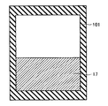
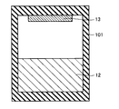
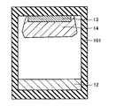
表1に示すように、第1の原料17を用いて第1のSiC結晶11を成長し、第1のSiC結晶11を粉砕して第2の原料12を形成し、第2の原料12を用いて第2のSiC結晶14を成長した本発明例1〜4は、比較例1よりもAlおよびFeの濃度を低減することができた。また、このように製造することで、0.1ppm以下の濃度のFeと、100ppm以下の濃度のAlとを含むSiC結晶を実現できることがわかった。
Claims (6)
- 炭化珪素結晶において、
鉄の濃度が0.002ppm以上0.1ppm以下であり、かつアルミニウムの濃度が0.02ppm以上100ppm以下であり、マイクロパイプ密度が2個/cm2以下であり、
前記炭化珪素結晶は、種基板と、前記種基板上に成長する結晶成長部とを備え、前記種基板および前記結晶成長部の双方が4H−SiCであることを特徴とする、炭化珪素結晶。 - エッチピット密度が4100個/cm2以上5200個/cm2以下であることを特徴とする、請求項1に記載の炭化珪素結晶。
- 第1の原料として研磨用炭化珪素粉末を準備する工程と、
前記第1の原料を加熱することにより昇華して、炭化珪素の結晶を析出することにより、第1の炭化珪素結晶を成長する工程と、
前記第1の炭化珪素結晶を粉砕して、第2の原料を形成する工程と、
前記第2の原料を加熱することにより昇華して、炭化珪素の結晶を析出することにより、第2の炭化珪素結晶を成長する工程とを備え、
前記第2の原料を形成する工程では、1μm以上3mm以下の範囲に粒度分布のピークが複数あり、各々の前記粒度分布のピークの中心の粒径から±50%の粒径の範囲に95%以上の粒子が存在するように前記第2の原料を形成する、炭化珪素結晶の製造方法。 - 前記第2の原料を形成する工程では、鉄の濃度が0.002ppm以上0.1ppm以下であり、かつアルミニウムの濃度が0.02ppm以上100ppm以下である前記第2の原料を形成する、請求項3に記載の炭化珪素結晶の製造方法。
- 前記第2の原料を形成する工程は、粉砕した前記第1の炭化珪素結晶を酸性溶液で洗浄する工程を含む、請求項3または4に記載の炭化珪素結晶の製造方法。
- 前記第2の炭化珪素結晶を粉砕して、第3の原料を形成する工程と、
前記第3の原料を加熱することにより昇華して、炭化珪素の結晶を析出することにより、第3の炭化珪素結晶を成長する工程とをさらに備えた、請求項3〜5のいずれか1項に記載の炭化珪素結晶の製造方法。
Priority Applications (10)
| Application Number | Priority Date | Filing Date | Title |
|---|---|---|---|
| JP2010100891A JP5565070B2 (ja) | 2010-04-26 | 2010-04-26 | 炭化珪素結晶および炭化珪素結晶の製造方法 |
| CN2011800043891A CN102597339A (zh) | 2010-04-26 | 2011-02-25 | 碳化硅晶体和制造碳化硅晶体的方法 |
| EP11774697.4A EP2565301B1 (en) | 2010-04-26 | 2011-02-25 | Silicon carbide crystal and method for producing silicon carbide crystal |
| KR1020127009040A KR20120130318A (ko) | 2010-04-26 | 2011-02-25 | 탄화규소 결정 및 탄화규소 결정의 제조 방법 |
| US13/499,482 US8574529B2 (en) | 2010-04-26 | 2011-02-25 | Silicon carbide crystal and method of manufacturing silicon carbide crystal |
| CA2775923A CA2775923A1 (en) | 2010-04-26 | 2011-02-25 | Silicon carbide crystal and method of manufacturing silicon carbide crystal |
| PCT/JP2011/054339 WO2011135913A1 (ja) | 2010-04-26 | 2011-02-25 | 炭化珪素結晶および炭化珪素結晶の製造方法 |
| TW100113266A TW201142092A (en) | 2010-04-26 | 2011-04-15 | Silicon carbide crystal and method for producing silicon carbide crystal |
| US14/019,882 US20140004303A1 (en) | 2010-04-26 | 2013-09-06 | Silicon carbide crystal and method of manufacturing silicon carbide crystal |
| US15/185,602 US9725823B2 (en) | 2010-04-26 | 2016-06-17 | Silicon carbide crystal and method of manufacturing silicon carbide crystal |
Applications Claiming Priority (1)
| Application Number | Priority Date | Filing Date | Title |
|---|---|---|---|
| JP2010100891A JP5565070B2 (ja) | 2010-04-26 | 2010-04-26 | 炭化珪素結晶および炭化珪素結晶の製造方法 |
Publications (3)
| Publication Number | Publication Date |
|---|---|
| JP2011230941A JP2011230941A (ja) | 2011-11-17 |
| JP2011230941A5 JP2011230941A5 (ja) | 2013-01-24 |
| JP5565070B2 true JP5565070B2 (ja) | 2014-08-06 |
Family
ID=44861234
Family Applications (1)
| Application Number | Title | Priority Date | Filing Date |
|---|---|---|---|
| JP2010100891A Active JP5565070B2 (ja) | 2010-04-26 | 2010-04-26 | 炭化珪素結晶および炭化珪素結晶の製造方法 |
Country Status (8)
| Country | Link |
|---|---|
| US (3) | US8574529B2 (ja) |
| EP (1) | EP2565301B1 (ja) |
| JP (1) | JP5565070B2 (ja) |
| KR (1) | KR20120130318A (ja) |
| CN (1) | CN102597339A (ja) |
| CA (1) | CA2775923A1 (ja) |
| TW (1) | TW201142092A (ja) |
| WO (1) | WO2011135913A1 (ja) |
Families Citing this family (8)
| Publication number | Priority date | Publication date | Assignee | Title |
|---|---|---|---|---|
| JP5910393B2 (ja) | 2012-07-26 | 2016-04-27 | 住友電気工業株式会社 | 炭化珪素基板の製造方法 |
| JP6028754B2 (ja) | 2014-03-11 | 2016-11-16 | トヨタ自動車株式会社 | SiC単結晶基板の製造方法 |
| US10108798B1 (en) * | 2016-01-04 | 2018-10-23 | Smart Information Flow Technologies LLC | Methods and systems for defending against cyber-attacks |
| CN105603530B (zh) * | 2016-01-12 | 2018-02-27 | 台州市一能科技有限公司 | 用于碳化硅晶体高速生长的原料及碳化硅晶体的生长方法 |
| JP6086167B2 (ja) * | 2016-03-18 | 2017-03-01 | 住友電気工業株式会社 | 炭化珪素基板の製造方法 |
| WO2018176302A1 (zh) * | 2017-03-30 | 2018-10-04 | 新疆天科合达蓝光半导体有限公司 | 用于生长SiC晶体的SiC原料的制备方法和制备装置 |
| KR102442731B1 (ko) * | 2021-12-23 | 2022-09-13 | 주식회사 쎄닉 | 탄화규소 분말 및 이를 이용하여 탄화규소 잉곳을 제조하는 방법 |
| KR102442730B1 (ko) * | 2021-12-23 | 2022-09-13 | 주식회사 쎄닉 | 탄화규소 분말, 이를 이용하여 탄화규소 잉곳을 제조하는 방법 및 탄화규소 웨이퍼 |
Family Cites Families (19)
| Publication number | Priority date | Publication date | Assignee | Title |
|---|---|---|---|---|
| JPS58147493A (ja) | 1982-02-12 | 1983-09-02 | フイリツプス・ペトロリユ−ム・コンパニ− | 熱分解法用の防汚剤 |
| JPS58187479A (ja) | 1982-04-27 | 1983-11-01 | Honda Motor Co Ltd | 可撓シ−ル材の外被材貼付方法 |
| JPH0645519B2 (ja) * | 1986-08-18 | 1994-06-15 | 三洋電機株式会社 | p型SiC単結晶の成長方法 |
| JPS6350393A (ja) * | 1986-08-20 | 1988-03-03 | Sanyo Electric Co Ltd | SiC単結晶の成長方法 |
| US5863325A (en) | 1995-05-31 | 1999-01-26 | Bridgestone Corporation | Process for producing high purity silicon carbide powder for preparation of a silicon carbide single crystal and single crystal |
| JP3934695B2 (ja) * | 1995-05-31 | 2007-06-20 | 株式会社ブリヂストン | 炭化ケイ素単結晶製造用高純度炭化ケイ素粉体の製造方法 |
| JP3590464B2 (ja) | 1995-12-08 | 2004-11-17 | 新日本製鐵株式会社 | 4h型単結晶炭化珪素の製造方法 |
| US7553373B2 (en) * | 2001-06-15 | 2009-06-30 | Bridgestone Corporation | Silicon carbide single crystal and production thereof |
| SE520968C2 (sv) * | 2001-10-29 | 2003-09-16 | Okmetic Oyj | Högresistiv monokristallin kiselkarbid och metod för dess framställning |
| JP4593099B2 (ja) * | 2003-03-10 | 2010-12-08 | 学校法人関西学院 | 単結晶炭化ケイ素の液相エピタキシャル成長法及びそれに用いられる熱処理装置 |
| US20060249073A1 (en) | 2003-03-10 | 2006-11-09 | The New Industry Research Organization | Method of heat treatment and heat treatment apparatus |
| JP4307913B2 (ja) | 2003-06-18 | 2009-08-05 | 新日本製鐵株式会社 | 高純度炭化珪素単結晶の製造方法 |
| JP2005239496A (ja) * | 2004-02-27 | 2005-09-08 | Nippon Steel Corp | 炭化珪素単結晶育成用炭化珪素原料と炭化珪素単結晶及びその製造方法 |
| JP4427470B2 (ja) | 2004-03-29 | 2010-03-10 | 新日本製鐵株式会社 | 炭化珪素単結晶の製造方法 |
| WO2006017074A2 (en) * | 2004-07-07 | 2006-02-16 | Ii-Vi Incorporated | Low-doped semi-insulating sic crystals and method |
| JP2007284306A (ja) * | 2006-04-19 | 2007-11-01 | Nippon Steel Corp | 炭化珪素単結晶及びその製造方法 |
| JP5562641B2 (ja) * | 2006-09-14 | 2014-07-30 | クリー インコーポレイテッド | マイクロパイプ・フリーの炭化ケイ素およびその製造方法 |
| JP2010083681A (ja) * | 2008-09-29 | 2010-04-15 | Bridgestone Corp | 炭化ケイ素単結晶の製造方法及び真空チャック |
| JP2010095397A (ja) * | 2008-10-15 | 2010-04-30 | Nippon Steel Corp | 炭化珪素単結晶及び炭化珪素単結晶ウェハ |
-
2010
- 2010-04-26 JP JP2010100891A patent/JP5565070B2/ja active Active
-
2011
- 2011-02-25 CN CN2011800043891A patent/CN102597339A/zh active Pending
- 2011-02-25 EP EP11774697.4A patent/EP2565301B1/en active Active
- 2011-02-25 KR KR1020127009040A patent/KR20120130318A/ko not_active Application Discontinuation
- 2011-02-25 US US13/499,482 patent/US8574529B2/en active Active
- 2011-02-25 WO PCT/JP2011/054339 patent/WO2011135913A1/ja active Application Filing
- 2011-02-25 CA CA2775923A patent/CA2775923A1/en not_active Abandoned
- 2011-04-15 TW TW100113266A patent/TW201142092A/zh unknown
-
2013
- 2013-09-06 US US14/019,882 patent/US20140004303A1/en not_active Abandoned
-
2016
- 2016-06-17 US US15/185,602 patent/US9725823B2/en active Active
Also Published As
| Publication number | Publication date |
|---|---|
| EP2565301A1 (en) | 2013-03-06 |
| CA2775923A1 (en) | 2011-11-03 |
| US20140004303A1 (en) | 2014-01-02 |
| US9725823B2 (en) | 2017-08-08 |
| EP2565301A4 (en) | 2013-11-27 |
| TW201142092A (en) | 2011-12-01 |
| CN102597339A (zh) | 2012-07-18 |
| EP2565301B1 (en) | 2015-03-25 |
| US20120183466A1 (en) | 2012-07-19 |
| WO2011135913A1 (ja) | 2011-11-03 |
| JP2011230941A (ja) | 2011-11-17 |
| US8574529B2 (en) | 2013-11-05 |
| KR20120130318A (ko) | 2012-11-30 |
| US20160289863A1 (en) | 2016-10-06 |
Similar Documents
| Publication | Publication Date | Title |
|---|---|---|
| JP5565070B2 (ja) | 炭化珪素結晶および炭化珪素結晶の製造方法 | |
| JP5706823B2 (ja) | SiC単結晶ウエハーとその製造方法 | |
| JP6037671B2 (ja) | SiCエピタキシャルウェハ及びその製造方法 | |
| CN107208311B (zh) | 碳化硅单晶块的制造方法和碳化硅单晶块 | |
| KR20130137247A (ko) | 탄화규소 단결정 기판 및 그 제조 방법 | |
| JP6624868B2 (ja) | p型低抵抗率炭化珪素単結晶基板 | |
| JP6742183B2 (ja) | 炭化珪素単結晶インゴットの製造方法 | |
| JP2017065986A (ja) | 低抵抗率炭化珪素単結晶基板の製造方法 | |
| JP2011162414A (ja) | 炭化珪素結晶の製造方法および炭化珪素結晶 | |
| JP5674009B2 (ja) | 高硬度導電性ダイヤモンド多結晶体およびその製造方法 | |
| JP2016098162A (ja) | 再生炭化ケイ素粉末の製造方法及び炭化ケイ素単結晶の製造方法 | |
| JP6329733B2 (ja) | 半導体ウェハのエッチング方法、半導体ウェハの製造方法および半導体ウェハの結晶欠陥検出方法 | |
| JP4494856B2 (ja) | 炭化珪素単結晶成長用種結晶とその製造方法及びそれを用いた結晶成長方法 | |
| JP5135545B2 (ja) | 炭化珪素単結晶インゴット育成用種結晶及びその製造方法 | |
| JP6304477B2 (ja) | 炭化珪素粉粒体及びその製造方法 | |
| JP6695182B2 (ja) | 炭化珪素単結晶成長用種結晶の製造方法及び炭化珪素単結晶インゴットの製造方法 | |
| US20240059570A1 (en) | Silicon carbide powder, method for manufacturing the same and method for manufacturing silicon carbide ingot using the same | |
| JP7298940B2 (ja) | 炭化珪素ウエハ及びその製造方法 | |
| KR102236397B1 (ko) | 탄화규소 웨이퍼 및 이를 적용한 반도체 소자 | |
| KR102218607B1 (ko) | 탄화규소의 분말의 제조 방법 | |
| JP2011051861A (ja) | AlN単結晶の製造方法および種基板 | |
| JP2011168425A (ja) | 炭化珪素原料の製造方法及びそれを用いた炭化珪素単結晶の製造方法 | |
| JP2014015394A (ja) | 炭化珪素結晶の製造方法 | |
| JP2015030659A (ja) | 単結晶の製造方法 |
Legal Events
| Date | Code | Title | Description |
|---|---|---|---|
| A621 | Written request for application examination |
Free format text: JAPANESE INTERMEDIATE CODE: A621 Effective date: 20121025 |
|
| A521 | Request for written amendment filed |
Free format text: JAPANESE INTERMEDIATE CODE: A523 Effective date: 20121129 |
|
| A131 | Notification of reasons for refusal |
Free format text: JAPANESE INTERMEDIATE CODE: A131 Effective date: 20140128 |
|
| A521 | Request for written amendment filed |
Free format text: JAPANESE INTERMEDIATE CODE: A523 Effective date: 20140325 |
|
| TRDD | Decision of grant or rejection written | ||
| A01 | Written decision to grant a patent or to grant a registration (utility model) |
Free format text: JAPANESE INTERMEDIATE CODE: A01 Effective date: 20140520 |
|
| A61 | First payment of annual fees (during grant procedure) |
Free format text: JAPANESE INTERMEDIATE CODE: A61 Effective date: 20140602 |
|
| R150 | Certificate of patent or registration of utility model |
Ref document number: 5565070 Country of ref document: JP Free format text: JAPANESE INTERMEDIATE CODE: R150 |
|
| R250 | Receipt of annual fees |
Free format text: JAPANESE INTERMEDIATE CODE: R250 |
|
| R250 | Receipt of annual fees |
Free format text: JAPANESE INTERMEDIATE CODE: R250 |
|
| R250 | Receipt of annual fees |
Free format text: JAPANESE INTERMEDIATE CODE: R250 |
|
| R250 | Receipt of annual fees |
Free format text: JAPANESE INTERMEDIATE CODE: R250 |
|
| R250 | Receipt of annual fees |
Free format text: JAPANESE INTERMEDIATE CODE: R250 |
|
| R250 | Receipt of annual fees |
Free format text: JAPANESE INTERMEDIATE CODE: R250 |
|
| R250 | Receipt of annual fees |
Free format text: JAPANESE INTERMEDIATE CODE: R250 |